US9106400B2 - Hybrid timing recovery for burst mode receiver in passive optical networks - Google Patents
Hybrid timing recovery for burst mode receiver in passive optical networks Download PDFInfo
- Publication number
- US9106400B2 US9106400B2 US13/658,341 US201213658341A US9106400B2 US 9106400 B2 US9106400 B2 US 9106400B2 US 201213658341 A US201213658341 A US 201213658341A US 9106400 B2 US9106400 B2 US 9106400B2
- Authority
- US
- United States
- Prior art keywords
- phase alignment
- coupled
- logic circuit
- adc
- coarse phase
- Prior art date
- Legal status (The legal status is an assumption and is not a legal conclusion. Google has not performed a legal analysis and makes no representation as to the accuracy of the status listed.)
- Expired - Fee Related, expires
Links
Images


Classifications
-
- H—ELECTRICITY
- H04—ELECTRIC COMMUNICATION TECHNIQUE
- H04L—TRANSMISSION OF DIGITAL INFORMATION, e.g. TELEGRAPHIC COMMUNICATION
- H04L7/00—Arrangements for synchronising receiver with transmitter
- H04L7/02—Speed or phase control by the received code signals, the signals containing no special synchronisation information
- H04L7/033—Speed or phase control by the received code signals, the signals containing no special synchronisation information using the transitions of the received signal to control the phase of the synchronising-signal-generating means, e.g. using a phase-locked loop
- H04L7/0334—Processing of samples having at least three levels, e.g. soft decisions
- H04L7/0335—Gardner detector
-
- H—ELECTRICITY
- H04—ELECTRIC COMMUNICATION TECHNIQUE
- H04L—TRANSMISSION OF DIGITAL INFORMATION, e.g. TELEGRAPHIC COMMUNICATION
- H04L7/00—Arrangements for synchronising receiver with transmitter
- H04L7/02—Speed or phase control by the received code signals, the signals containing no special synchronisation information
- H04L7/033—Speed or phase control by the received code signals, the signals containing no special synchronisation information using the transitions of the received signal to control the phase of the synchronising-signal-generating means, e.g. using a phase-locked loop
- H04L7/0331—Speed or phase control by the received code signals, the signals containing no special synchronisation information using the transitions of the received signal to control the phase of the synchronising-signal-generating means, e.g. using a phase-locked loop with a digital phase-locked loop [PLL] processing binary samples, e.g. add/subtract logic for correction of receiver clock
Definitions
- a passive optical network is one system for providing network access over “the last mile.”
- the PON is a point to multi-point network comprised of an optical line terminal (OLT) at the central office, an optical distribution network (ODN), and a plurality of optical network units (ONUs) at the customer premises.
- Time Division Multiplexing (TDM) PONs such as Gigabit PONs (GPONs) and Ethernet PONs (EPONs), can serve potentially millions of users worldwide.
- TDM Time Division Multiplexing
- GPONs Gigabit PONs
- EPONs Ethernet PONs
- downstream data is broadcasted at about 2.5 Gigabits per second (Gbps) while upstream data is transmitted at about 1.25 Gbps.
- Gbps Gigabits per second
- upstream data is transmitted at about 1.25 Gbps.
- the bandwidth capability of the PON systems is expected to increase as the demands for services increase.
- the logic devices in emerging PON systems such as Next Generation Access (NGA) are being reconfigured
- Optical network units utilizing such technology commonly share upstream bandwidth using time division multiple access (TDMA) schemes. More specifically, data from ONUs are sent to optical line terminals (OLTs) burst-by-burst. Burst data from different ONUs frequently contains analog signals of different amplitudes and phases.
- TDMA time division multiple access
- burst-mode clock and data recovery in a short time period is desirable for compliance with the relevant standards.
- ITU-T International Telecommunication Union Telecommunication Standardization Sector
- Prior approaches to burst-mode clock and data recovery included phase locked loops (either analog or digital) and fast clock recovery circuitry. Because phase locked loops require thousands of bits to achieve suitable phase locking, conventional PON systems use fast clock recovery circuitry.
- Conventional fast clock recovery circuits generally employ one of two approaches: gated voltage controlled oscillators (gated VCOs) or over-sampling. Gated VCO systems are inexpensive but demonstrate relatively poor performance characteristics. Over-sampling systems demonstrate relatively better performance characteristics but are expensive and difficult to implement as data rate in PON upstream increases. Thus, a need exists for a relatively low-cost means for clock and data recovery for burst mode transmissions with relatively good performance characteristics.
- the disclosure includes an apparatus for coarse phase alignment of an analog signal comprising: a tapped delay line, a coarse phase alignment logic circuit coupled to the tapped delay line, and a selector coupled to the tapped delay and the coarse phase alignment logic circuit.
- the disclosure includes an apparatus for timing and data recovery for burst mode receivers comprising: a receiver, a coarse phase alignment circuit coupled to the receiver, at least one analog to digital converter (ADC) coupled to the coarse phase alignment circuit such that the coarse phase alignment circuit is positioned between the receiver and the ADC, and a fine phase alignment circuit coupled to the ADC such that the ADC is positioned between the coarse phase alignment circuit and the fine phase alignment circuit, wherein the fine phase alignment circuit produces a recovered data output.
- ADC analog to digital converter
- the disclosure includes a method of burst mode clock and data recovery at an OLT in a PON comprising the steps of: receiving an upstream analog signal, aligning a coarse phase for the upstream analog signal, converting the coarse phase aligned upstream analog signal to a digital signal, aligning a fine phase for the digital signal, and outputting a recovered data signal.
- FIG. 1 depicts a schematic diagram of an embodiment of a PON.
- FIG. 2 depicts a schematic diagram of an embodiment of a gated VCO system.
- FIG. 3 depicts a schematic diagram of another embodiment of a gated VCO system.
- FIG. 4 depicts schematic diagram of an embodiment of an over-sampling system.
- FIG. 5 depicts schematic diagram of another embodiment of an over-sampling system.
- FIG. 6 depicts a schematic diagram of an embodiment of a hybrid timing and data recovery for burst-mode receiver.
- FIG. 7 depicts a schematic diagram of another embodiment of a hybrid timing and data recovery for burst-mode receiver.
- FIG. 8 depicts the comparator and clock outputs corresponding to FIG. 7 .
- FIG. 9 depicts a truth table corresponding to FIGS. 7 and 8 .
- FIG. 10 depicts a schematic diagram of another embodiment of a hybrid timing and data recovery for burst-mode receiver.
- FIG. 11 is a schematic diagram of an embodiment of a general-purpose computer system.
- hybrid approaches use over-sampling techniques for rapid coarse phase alignment followed by digital timing recovery techniques for fine phase alignment.
- the two-step approach coarsely aligns the phase of the analog signal using over-sampling, converts the analog signal to digital, and finely aligns the phase of the digital signal using digital timing recovery techniques. Consequently, such hybrid approaches combine the fast phase locking and superior jitter tolerance of previous approaches to burst mode timing recovery.
- FIG. 1 depicts a schematic diagram of an embodiment of a PON 100 .
- the PON 100 comprises an OLT 110 , a plurality of ONUs 120 , and an ODN 130 , which may be coupled to the OLT 110 and the ONUs 120 .
- the PON 100 may be a communications network that does not require any active components to distribute data between the OLT 110 and the ONUs 120 . Instead, the PON 100 may use the passive optical components in the ODN 130 to distribute data between the OLT 110 and the ONUs 120 .
- the PON 100 may be a Next Generation Access (NGA) system, such as a ten Gbps GPON (XGPON), which may have a downstream bandwidth of about ten Gbps and an upstream bandwidth of at least about 2.5 Gbps.
- NGA Next Generation Access
- the PON 100 may be any Ethernet based network, such as an EPON defined by the Institute of Electrical and Electronics Engineers (IEEE) 802.3ah standard, a 10 Gigabit EPON as defined by the IEEE 802.3av standard, an asynchronous transfer mode PON (APON), a broadband PON (BPON) defined by the ITU-T G.983 standard, a GPON defined by the ITU-T G.984 standard, a wavelength division multiplexed (WDM) PON (WPON), or a suitable after-arising technology, all of which are incorporated herein by reference as if reproduced in their entirety.
- IEEE Institute of Electrical and Electronics Engineers
- APON asynchronous transfer mode PON
- BPON broadband
- the OLT 110 may be any device configured to communicate with the ONUs 120 and another network (not shown). Specifically, the OLT 110 may act as an intermediary between the other network and the ONUs 120 . For instance, the OLT 110 may forward data received from the network to the ONUs 120 , and forward data received from the ONUs 120 onto the other network. Although the specific configuration of the OLT 110 may vary depending on the type of PON 100 , in an embodiment, the OLT 110 may comprise a transmitter and a receiver.
- the OLT 110 may comprise a converter that converts the network protocol into the PON protocol.
- the OLT 110 converter may also convert the PON protocol into the network protocol.
- the OLT 110 may be typically located at a central location, such as a central office, but may be located at other locations as well.
- the ONUs 120 may be any devices that are configured to communicate with the OLT 110 and a customer or user (not shown). Specifically, the ONUs 120 may act as an intermediary between the OLT 110 and the customer. For instance, the ONUs 120 may forward data received from the OLT 110 to the customer, and forward data received from the customer onto the OLT 110 . Although the specific configuration of the ONUs 120 may vary depending on the type of PON 100 , in an embodiment, the ONUs 120 may comprise an optical transmitter configured to send optical signals to the OLT 110 and an optical receiver configured to receive optical signals from the OLT 110 .
- the ONUs 120 may comprise a converter that converts the optical signal into electrical signals for the customer, such as signals in the Ethernet or asynchronous transfer mode (ATM) protocol, and a second transmitter and/or receiver that may send and/or receive the electrical signals to a customer device.
- ATM asynchronous transfer mode
- ONUs 120 and optical network terminals (ONTs) are similar, and thus the terms are used interchangeably herein.
- the ONUs 120 may be typically located at distributed locations, such as the customer premises, but may be located at other locations as well.
- the ODN 130 may be a data distribution system, which may comprise optical fiber cables, couplers, splitters, distributors, and/or other equipment.
- the optical fiber cables, couplers, splitters, distributors, and/or other equipment may be passive optical components.
- the optical fiber cables, couplers, splitters, distributors, and/or other equipment may be components that do not require any power to distribute data signals between the OLT 110 and the ONUs 120 .
- the ODN 130 may comprise one or a plurality of active components, such as optical amplifiers.
- the ODN 130 may typically extend from the OLT 110 to the ONUs 120 in a branching configuration as shown in FIG. 1 , but may be alternatively configured in any other point-to-multi-point configuration.
- FIGS. 2 and 3 depict schematic diagrams of gated VCO systems 140 , 141 .
- two oscillators 145 , 146 are gated by the input burst mode data sequence 150 .
- oscillator 145 produces periodical clock pulses while oscillator 146 is off.
- the combination of both oscillators' 145 , 146 outputs results in a continuous clock corresponding roughly to the bit rate of the input data.
- FIG. 3 operates according to substantially the same principles.
- Gated VCO systems have the advantage of simplicity and, consequently, low cost. Gated VCO systems may recover the clock within one bit. However, gated VCOs rely on oscillators whose frequency differs slightly, producing some amount of deterministic jitter on the recovered clock depending on the received data pattern. Further, the random jitter from the data passes through to the recovered clock without any filtering, creating poor overall performance.
- FIGS. 4 and 5 depict schematic diagrams of over-sampling systems.
- FIG. 4 represents a demonstration of burst-mode timing and data recovery with over-sampling.
- FIG. 5 represents an implementation of over-sampling for 10 Gbps burst-mode receivers.
- a fast sampler produces a few samples for each incoming bit (typically 8 samples per bit).
- a digital logic selects a sampling time (corresponding to one of the sample in each bit) for data recovery.
- Over-sampling approaches provide better jitter performance than gated VCO approaches. By utilizing a few samples for each incoming bit, over-sampling systems may achieve better overall performance than gated VCO systems. However, the number of samples per bit results in sampling rates well in excess of data rates. Over-sampling generally requires a fast sampler and hence generally costs more than gated VCO systems. For example, an XGPON system with a 2.5 Gbps upstream data rate may require 20 Gbps sampling. Samplers capable of such sampling rates are expensive and difficult to implement with current technology.
- FIG. 6 depicts a schematic diagram of one embodiment of a hybrid timing and data recovery for burst-mode receiver, which may be used in the OLT and/or ONU described above under the discussion of FIG. 1 .
- the hybrid timing and data recovery for burst-mode receiver may comprise a coarse phase alignment circuit 205 that performs a coarse phase alignment on a received signal 200 (which may be an analog signal), and one or more ADCs 245 that convert the coarse phase aligned analog signal(s) into one or more digital signals.
- the hybrid timing and data recovery for burst-mode receiver may also comprise a fine phase alignment circuit 250 that performs a fine phase alignment on the digital signal(s), and a comparator 260 that compares the fine phase aligned digital signal with one or more thresholds and produces the recovered data 280 . Further details of the coarse phase alignment circuit 205 , the ADCs 245 , the fine phase alignment circuit 250 , and the comparator 260 are provided below.
- a received signal 200 may enter the coarse phase alignment circuit 205 at a tapped delay line 210 .
- the tapped delay line 210 may delay the received signal 200 for some predetermined time, and may divide the received signal 200 into two or more delayed signals.
- the resulting N delayed, divided signals may each be further split and one version passed to each of a plurality of flip-flops 215 and a selector 240 .
- the flip-flops 215 may be gated D-latches, though suitable alternatives to gated D-latch flip-flops exist and are within the scope of this disclosure as will be understood to one having ordinary skill in the relevant art.
- the number of flip-flops 215 may directly correspond to N.
- the flip-flops 215 may receive a modified (e.g., half) or an unmodified rate input from system clock 220 , where modified rate input may be preferred to utilize a single ADC 245 and an umodified rate input may be useful for utilizing multiple ADCs 245 , as discussed further herein.
- the D flip-flop may optionally be level triggered or edge triggered within the scope of this disclosure.
- the coarse phase alignment logic circuit 230 may select M out of the N delayed versions of the received signal 200 using a processing routine further described under the discussion of FIG. 8 .
- the coarse phase alignment logic circuit 230 may subsequently inform the N to M selector 240 which M out of the N delayed versions of the received signal 200 to select using one or more selection signals as may be needed to identify.
- N to M selector 240 also referred to as a demultiplexer or demux, may receive the N delayed signals from tapped delay line 210 as well as the selection signal(s) from the coarse phase alignment logic circuit 230 .
- the selection signal(s) from the coarse phase alignment logic circuit 230 may instruct N to M selector 240 which M of the N delayed signals coarsely aligns with the clock, and N to M selector 240 may forward the selected M signals to the ADCs 245 .
- the coarse phase alignment circuit 205 may align the received signal 200 (e.g., a preamble) and clock 220 (e.g., the center of the bit period coarsely aligns with the falling edge of the clock signal) within T b /N. After the preamble, the coarse phase alignment logic locks and the selection signal(s) is sustained over the remaining burst period. Alternately, the coarse phase alignment and selection signal(s) may be readjusted as needed after the preamble.
- Data may pass out of the coarse phase alignment circuit 205 at N to M selector 240 to the ADCs 245 .
- the ADCs 245 are well known in the art, and each ADC 245 may run at the nominal bit rate and may convert one of the analog signals from N to M selector 240 into a digital signal. The digital signals output from ADCs 245 may then be sent to the fine phase alignment circuit 250 .
- the fine phase alignment circuit 250 may use a conventional digital loop with interpolator 255 .
- the digital outputs of ADCs 245 may enter the fine phase alignment circuit 250 at interpolator 255 .
- Interpolator 255 may measure the fraction of a clock period, e.g., the time between a clock event and the event being measured, and may be a ramp interpolator, a vernier interpolator, or other suitable device as known in the art.
- the output of interpolator 255 may be split with one signal going to a comparator 260 and another signal going to a timing error estimator 265 .
- the timing error estimator 265 may pass the resulting data to a loop filter 270 , which may determine the noise and/or jitter of the signal and the associated filtering required to improve the signal quality.
- the loop filter 270 may pass the resulting data back to interpolator 255 as feedback for noise and/or jitter tolerance control.
- the output of the fine phase alignment circuit 250 may be sent to a comparator 260 .
- Comparator 260 may further receive a threshold parameter, and may compare the output of interpolator 255 to the threshold parameter.
- the comparator 260 may output recovered data 280 as a sequence of bits, wherein a “1” is output when the output of interpolator 255 is above the threshold and a “0” is output when the output of interpolator 255 is at or below the threshold.
- FIG. 7 depicts a schematic diagram of another embodiment of a hybrid timing and data recovery for burst-mode receiver, which may be used in the OLT and/or ONU described above.
- the hybrid timing and data recovery for burst-mode receiver of the depicted embodiment comprises: a received signal 300 , a coarse phase alignment circuit 305 comprising a tapped delay line 310 , a plurality of flip flops 315 , a coarse phase alignment logic circuit 330 , and a 4:1 selector 340 ; an ADC 345 ; a fine phase alignment circuit 350 comprising an interpolator 355 , a timing error estimator 365 , and a loop filter 370 ; a clock 320 ; and a comparator 360 having a recovered data output 380 .
- FIG. 7 includes outputs Q 3 , Q 2 , Q 1 and Q 0 from flip-flops 315 for correlation with FIGS. 8 and 9 , discussed further below.
- the N and M values have been assigned as 4 and 1, respectively.
- the tapped delay line 310 delays the received signal 300 by 0, 0.25 T b , 0.50 T b , and 0.75 T b
- a 4 to 1 selector 340 replaces N to M selector 240
- two selection signals, SEL 1 and SEL 0 are sent from coarse phase alignment circuit 305 to 4 to 1 selector 340 .
- Two selection signals, SEL 1 and SEL 0 may be used to designate 1 of the 4 delayed signals as the signal to pass to ADCs 345 .
- more delayed signals are used and, consequently, more selection signals may be required to instruct the N to M selector 240 which delayed signal to pass to ADCs 245 .
- only two delayed signals are used and, consequently, only one selection signal may be needed to select the appropriate delayed signal.
- FIG. 8 depicts the timing diagram for the delayed versions of the receiver preambles for received signal 300 of FIG. 7 , as well as their alignment with respect to the clock 320 and a half-rate clock 320 as input to the flip-flops 315 .
- FIG. 9 depicts a truth table corresponding to FIGS. 7 and 8 .
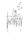
- FIG. 10 depicts a schematic diagram of still another embodiment of a hybrid timing and data recovery for burst-mode receiver, which may be used in the OLT and/or ONU described above.
- the hybrid timing and data recovery for burst-mode receiver of the depicted embodiment comprises: a received signal 400 , a coarse phase alignment circuit 405 comprising a tapped delay line 410 , a plurality of flip flops 415 , a coarse phase alignment logic circuit 430 , and a 4:1 selector 440 ; an ADC 445 ; a fine phase alignment circuit 450 comprising a timing error estimator 465 and a phase shifter 475 ; a clock 420 ; and a comparator 460 having a recovered data output 480 .
- Fine phase alignment circuit 450 comprises a timing error estimator 465 and a phase shifter 475 that may phase-shift clock 420 input to ADC 445 .
- the amount of phase shift may be proportional to the timing error produced by timing error estimator 450 , and phase shifter 475 may be adjusted to finely align the sampling time of ADC 445 .
- Certain embodiments further utilize a phase shifter 475 on the clock path, the signal path, or both. When a phase shifter 475 is located on the signal path, the phase shifter may optionally be located prior to the tap delay line 410 or between the ADC 445 and the selector 440 .
- coarse phase alignment logic circuit 230 samples un-delayed received signal 200 using delayed versions of the clock signal, where each clock signal is delayed by a fraction of the bit period. Such an embodiment functions in substantially the same way as detailed above, but selects the delayed clock signal most closely approximating received signal 200 to align the coarse phase.
- timing error estimator 265 may use other algorithms instead of or in conjunction with the algorithms disclosed herein as will be understood by one having ordinary skill in the relevant art.
- different loop filters may replace loop filter 270 based on the desired convergence time and jitter tolerance of the digital timing recovery loop as will be understood by one having ordinary skill in the relevant art.
- Acceptable loop filters include various low pass filters known in the art.
- FIG. 11 illustrates a typical, general-purpose network component or computer system 600 suitable for implementing one or more embodiments of methods disclosed herein, such as one or more steps of method 200 .
- the general-purpose network component or computer system 600 includes a processor 602 (which may be referred to as a central processor unit or CPU) that is in communication with memory devices including secondary storage 604 , read only memory (ROM) 606 , random access memory (RAM) 608 , input/output (I/O) 610 devices, and network connectivity devices 612 .
- ROM read only memory
- RAM random access memory
- I/O input/output
- the processor 602 may be implemented as one or more CPU chips, or one or more cores (e.g., a multi-core processor), or may be part of one or more application specific integrated circuits (ASICs) and/or digital signal processors (DSPs).
- the processor 602 may be configured to implement any of the schemes described herein, including one or more steps of the described signal processing method, which may be implemented using hardware, software, or both.
- the secondary storage 604 is typically comprised of one or more disk drives or tape drives and is used for non-volatile storage of data and as an over-flow data storage device if RAM 608 is not large enough to hold all working data. Secondary storage 604 may be used to store programs that are loaded into RAM 608 when such programs are selected for execution.
- the ROM 606 is used to store instructions and perhaps data that are read during program execution. ROM 606 is a non-volatile memory device that typically has a small memory capacity relative to the larger memory capacity of secondary storage.
- the RAM 608 is used to store volatile data and perhaps to store instructions. Access to both ROM 606 and RAM 608 is typically faster than to secondary storage 604 .
- R Rl+k*(Ru ⁇ Rl)
- k is a variable ranging from 1 percent to 100 percent with a 1 percent increment, i.e., k is 1 percent, 2 percent, 3 percent, 4 percent, 5 percent, . . . , 50 percent, 51 percent, 52 percent, . . . , 95 percent, 96 percent, 97 percent, 98 percent, 99 percent, or 100 percent.
- any numerical range defined by two R numbers as defined in the above is also specifically disclosed.
Landscapes
- Engineering & Computer Science (AREA)
- Computer Networks & Wireless Communication (AREA)
- Signal Processing (AREA)
- Synchronisation In Digital Transmission Systems (AREA)
Abstract
Description
t d,k =kT b /N+MT b
where k=0, 1, 2, . . . , N−1, Tb is the bit period, N may be any integer selected based on the number of desired signals, and M is an integer that is based on the number of desired signals output to the
e n=(y n −y n-2)·y n-1
where yn is the current sample, yn-1 is the previous sample, yn-2 is the sample prior to yn-1, the spacing between yn and yn-2 is T seconds, and the spacing between yn and yn-1 is T/2 seconds. The
S1=Q 3 Q 2 Q 1 Q 0 +
S0=
-
- (where ⊕ denotes exclusive or)
or the truth table depicted inFIG. 8 , where Q3, Q2, Q1 and Q0 are the inputs to the coarse phasealignment logic circuit 330 which are output from the flip-flops 315, as depicted inFIG. 7 . The input values (Q3, Q2, Q1 and Q0) in the lower portion of the truth table ofFIG. 8 do not occur in real implementations, and consequently are disregarded. In an embodiment, the coarse phasealignment logic circuit 330 may align the receivedsignal 300 and the clock 320 (e.g., the center of the bit period is coarsely aligned with the falling edge of the half-rate clock 320), as shown inFIG. 8 , within 0.25 Tb. If the coarse phasealignment logic circuit 330 determines, for example, that delayed signal D3 most closely aligns with the falling edge of the half-rate clock 320, as shown inFIG. 8 , SEL1 and SEL0 may lock as 0/0, as shown inFIG. 9 . In addition, the coarse phasealignment logic circuit 330 may send selection signals SEL1 and SEL0 to the 4 to 1selector 340, as shown inFIG. 9 , informing the 4 to 1selector 340 which delayed signal from the tappeddelay line 310 should be passed to theADC 345. After the preamble, the phase alignment logic may lock, and the selection signals SEL1 and SEL0 may remain constant over the remaining burst period.
- (where ⊕ denotes exclusive or)
e n=(y n ·ŷ n-1)−(ŷ n ·y n-1)
wherein yn is the current sample, yn-1 is the previous sample, ŷn is the decision made by the current sample, and ŷn-1 is the decision made by the previous sample. Certain embodiments further utilize a
Claims (19)
Priority Applications (2)
| Application Number | Priority Date | Filing Date | Title |
|---|---|---|---|
| US13/658,341 US9106400B2 (en) | 2012-10-23 | 2012-10-23 | Hybrid timing recovery for burst mode receiver in passive optical networks |
| PCT/CN2013/085761 WO2014063623A1 (en) | 2012-10-23 | 2013-10-23 | Hybrid timing recovery for burst mode receiver in passive optical networks |
Applications Claiming Priority (1)
| Application Number | Priority Date | Filing Date | Title |
|---|---|---|---|
| US13/658,341 US9106400B2 (en) | 2012-10-23 | 2012-10-23 | Hybrid timing recovery for burst mode receiver in passive optical networks |
Publications (2)
| Publication Number | Publication Date |
|---|---|
| US20140112356A1 US20140112356A1 (en) | 2014-04-24 |
| US9106400B2 true US9106400B2 (en) | 2015-08-11 |
Family
ID=50485287
Family Applications (1)
| Application Number | Title | Priority Date | Filing Date |
|---|---|---|---|
| US13/658,341 Expired - Fee Related US9106400B2 (en) | 2012-10-23 | 2012-10-23 | Hybrid timing recovery for burst mode receiver in passive optical networks |
Country Status (2)
| Country | Link |
|---|---|
| US (1) | US9106400B2 (en) |
| WO (1) | WO2014063623A1 (en) |
Cited By (2)
| Publication number | Priority date | Publication date | Assignee | Title |
|---|---|---|---|---|
| US20170111184A1 (en) * | 2015-02-05 | 2017-04-20 | Crrc Qingdao Sifang Rolling Stock Research Institute Co., Ltd. | Protocol converter between cpci bus and isa bus and conversion method thereof |
| US11086002B1 (en) * | 2015-04-21 | 2021-08-10 | Maxim Integrated Products, Inc. | Ultrasound sub-array receiver beamformer |
Families Citing this family (2)
| Publication number | Priority date | Publication date | Assignee | Title |
|---|---|---|---|---|
| US9544061B2 (en) | 2015-03-04 | 2017-01-10 | Alcatel-Lucent Usa Inc. | Switched optical receiver |
| US10560097B1 (en) * | 2018-09-28 | 2020-02-11 | Teletrx Co. | High-speed 4:1 multiplexer for voltage-mode transmitter with automatic phase alignment technique |
Citations (66)
| Publication number | Priority date | Publication date | Assignee | Title |
|---|---|---|---|---|
| US3839599A (en) * | 1972-11-10 | 1974-10-01 | Gte Automatic Electric Lab Inc | Line variation compensation system for synchronized pcm digital switching |
| US3922613A (en) * | 1975-01-02 | 1975-11-25 | Honeywell Inf Systems | Information detection apparatus having an adaptive digital tracking oscillator |
| US4119006A (en) * | 1977-02-24 | 1978-10-10 | Allen Organ Company | Continuously variable attack and decay delay for an electronic musical instrument |
| US4513427A (en) * | 1982-08-30 | 1985-04-23 | Xerox Corporation | Data and clock recovery system for data communication controller |
| US4617679A (en) * | 1983-09-20 | 1986-10-14 | Nec Electronics U.S.A., Inc. | Digital phase lock loop circuit |
| US4868514A (en) * | 1987-11-17 | 1989-09-19 | International Business Machines Corporation | Apparatus and method for digital compensation of oscillator drift |
| US5081655A (en) * | 1989-10-23 | 1992-01-14 | Northern Telecom Limited | Digital phase aligner and method for its operation |
| US5155487A (en) * | 1990-03-02 | 1992-10-13 | Hitachi, Ltd. | Cell delineation method and cell delineation circuit |
| US5293170A (en) * | 1991-04-10 | 1994-03-08 | Ashtech Inc. | Global positioning system receiver digital processing technique |
| US5305322A (en) * | 1989-06-23 | 1994-04-19 | Nec Corporation | Phase alignment circuit for stuffed-synchronized TDM transmission system with cross-connect function |
| US5394024A (en) * | 1992-12-17 | 1995-02-28 | Vlsi Technology, Inc. | Circuit for eliminating off-chip to on-chip clock skew |
| US5550514A (en) * | 1993-04-28 | 1996-08-27 | Telefonaktiebolaget Lm Ericsson | Digital controlled xtal osc |
| US5589788A (en) * | 1994-05-12 | 1996-12-31 | Hewlett-Packard Company | Timing adjustment circuit |
| US5768283A (en) * | 1994-11-08 | 1998-06-16 | Washington University | Digital phase adjustment circuit for asynchronous transfer mode and like data formats |
| US5799051A (en) * | 1992-05-28 | 1998-08-25 | Rambus, Inc. | Delay stage circuitry for a ring oscillator |
| US5945862A (en) * | 1997-07-31 | 1999-08-31 | Rambus Incorporated | Circuitry for the delay adjustment of a clock signal |
| US5955907A (en) * | 1995-03-03 | 1999-09-21 | Advantest Corp. | Temperature compensation circuit and method for providing a constant delay |
| US6031401A (en) * | 1998-06-08 | 2000-02-29 | Tritech Microelectronics, Ltd. | Clock waveform synthesizer |
| US6128359A (en) * | 1998-10-27 | 2000-10-03 | Intel Corporation | Phase difference magnifier |
| US6208667B1 (en) * | 1997-09-19 | 2001-03-27 | Fujitsu Network Communications | Constant phase crossbar switch |
| US20020054409A1 (en) * | 2000-09-05 | 2002-05-09 | Meir Bartur | Fiber optic transceiver employing clock and data phase aligner |
| US20030012322A1 (en) * | 2001-06-22 | 2003-01-16 | Torsten Partsch | Delay locked loop |
| US20030058930A1 (en) * | 1998-04-15 | 2003-03-27 | Fujitsu, Ltd. | Signal processor having feedback loop control for decision feedback equalizer |
| US6549596B1 (en) * | 1998-09-17 | 2003-04-15 | Stmicroelectronics S.R.L. | Fully digital phase aligner |
| US20030155490A1 (en) * | 1998-02-25 | 2003-08-21 | Muriel Medard | Method and apparatus for detecting malfunctions in communication systems |
| US20030215039A1 (en) * | 2002-05-14 | 2003-11-20 | Block Stefan G. | Digital multi-phase clock generator |
| US6658457B2 (en) * | 1999-03-19 | 2003-12-02 | Fujitsu Limited | Device and method for interconnecting distant networks through dynamically allocated bandwidth |
| US20040022311A1 (en) * | 2002-07-12 | 2004-02-05 | Zerbe Jared L. | Selectable-tap equalizer |
| US20040116160A1 (en) * | 2002-12-09 | 2004-06-17 | Acuid Corporation (Guernsey) Limited | Simultaneous bidirectional differential signalling interface |
| US20040247041A1 (en) * | 2003-06-04 | 2004-12-09 | Tropian, Inc., A California Corporation | Digital time alignment in a polar modulator |
| US20050007165A1 (en) * | 2003-07-08 | 2005-01-13 | Ati Technologies, Inc. | Method and apparatus for determining a processing speed of an integrated circuit |
| US20050163252A1 (en) * | 2004-01-27 | 2005-07-28 | Crestcom, Inc. | Transmitter predistortion circuit and method therefor |
| US20050270073A1 (en) * | 2004-06-07 | 2005-12-08 | Yong-Mi Lee | Glitch-free clock switching apparatus |
| US20060071698A1 (en) * | 2004-10-01 | 2006-04-06 | Parag Parikh | Digital phase shift circuits |
| US20060098771A1 (en) * | 2004-11-08 | 2006-05-11 | Cafaro Nicholas G | Method and apparatus for a digital-to-phase converter |
| US20060120733A1 (en) * | 2000-10-05 | 2006-06-08 | Tucker Rodney S | System and method for optical heterodyne detection of an optical signal including optical pre-selection that is adjusted to accurately track a local oscillator signal |
| US20060145741A1 (en) * | 2004-12-30 | 2006-07-06 | Stmicroelectronics Pvt. Ltd. | Digital delay lock loop |
| US20060198634A1 (en) * | 2005-03-07 | 2006-09-07 | Nettest North America, Inc. | Passive optical network loss test apparatus and method of use thereof |
| US7123882B1 (en) * | 2000-03-03 | 2006-10-17 | Raytheon Company | Digital phased array architecture and associated method |
| US20060273836A1 (en) * | 2004-07-22 | 2006-12-07 | Feng Lin | Method and apparatus to set a tuning range for an analog delay |
| US20080025733A1 (en) * | 2006-06-27 | 2008-01-31 | Technion Research & Development Foundation Ltd. | Optical differential phase shift keying receivers with multi-symbol decision feedback-based electro-optic front-end processing |
| US20090028554A1 (en) * | 2005-10-13 | 2009-01-29 | National Ict Australia Limited | Method and apparatus for sampled optical signal monitoring |
| US7502278B1 (en) * | 2006-05-23 | 2009-03-10 | Maxim Integrated Products, Inc. | Analog beamformers for continuous wave ultrasonic receivers |
| US20090129446A1 (en) * | 2007-11-16 | 2009-05-21 | Motorola, Inc. | Method and apparatus for generating phase shifted local oscillator signals for a feedback loop on a transmitter |
| US20090201796A1 (en) * | 2008-02-13 | 2009-08-13 | Nortel Networks Limited | Low conversion rate digital dispersion compensation |
| US20090256622A1 (en) * | 2008-04-11 | 2009-10-15 | Nortel Networks Limited | Soft thermal failure in a high capacity transmission system |
| US20100135652A1 (en) * | 2007-08-13 | 2010-06-03 | Huawei Technologies Co., Ltd. | Fault detecting method, system, and apparatus for pon system |
| US7773667B2 (en) * | 2005-07-14 | 2010-08-10 | Agere Systems Inc. | Pseudo asynchronous serializer deserializer (SERDES) testing |
| US7773713B2 (en) * | 2006-10-19 | 2010-08-10 | Motorola, Inc. | Clock data recovery systems and methods for direct digital synthesizers |
| US20100315141A1 (en) * | 2009-06-12 | 2010-12-16 | Freescale Semiconductor, Inc. | Multiple-stage, signal edge alignment apparatus and methods |
| US20100321072A1 (en) * | 2007-11-20 | 2010-12-23 | Imec | Device and Method for Signal Detection in a TDMA Network |
| CN101931398A (en) | 2009-06-26 | 2010-12-29 | 国际商业机器公司 | Method and device for closed-loop clock correction |
| US20110018748A1 (en) * | 2009-07-27 | 2011-01-27 | Lsi Corporation | Systems and Methods for Two Tier Sampling Correction in a Data Processing Circuit |
| US20110185215A1 (en) * | 2010-01-28 | 2011-07-28 | Futurewei Technologies, Inc. | Single-Wire Serial Interface |
| US20110298511A1 (en) * | 2010-06-04 | 2011-12-08 | Xilinx, Inc. | Strobe signal management to clock data into a system |
| US20110317752A1 (en) * | 2010-06-28 | 2011-12-29 | Phyworks Limited | Equalizer adaptation |
| US8111993B2 (en) * | 2005-10-12 | 2012-02-07 | Ofidium Pty Ltd. | Methods and apparatus for optical transmission of digital signals |
| US20120062331A1 (en) | 2010-09-10 | 2012-03-15 | Ashoke Ravi | System, method and apparatus for an open loop calibrated phase wrapping phase modulator for wideband rf outphasing/polar transmitters |
| US20120099857A1 (en) * | 2009-06-11 | 2012-04-26 | Hisense Broadband Multimedia Technologies Co., Ltd | Optical line terminal |
| US20120304241A1 (en) * | 2009-12-15 | 2012-11-29 | Broadcom Corporation | Rf signal transport over passive optical networks |
| US20120313683A1 (en) * | 2011-06-10 | 2012-12-13 | International Business Machines Corporation | Programmable delay generator and cascaded interpolator |
| US20130016982A1 (en) * | 2011-07-15 | 2013-01-17 | Intel Mobile Communications GmbH | Adjustable delayer, method for delaying an input signal and polar transmitter |
| US20130021073A1 (en) * | 2004-05-18 | 2013-01-24 | Kang Yong Kim | Dll phase detection using advanced phase equalization |
| US20130120170A1 (en) * | 2011-11-14 | 2013-05-16 | Texas Instruments Incorporated | Pipelined adc with a vco-based stage |
| US20130216228A1 (en) * | 2010-06-22 | 2013-08-22 | Moshe Nazarathy | Optical network unit, optical access network and a method for exchanging information |
| US20130259174A1 (en) * | 2012-04-02 | 2013-10-03 | Nec Laboratories America, Inc. | Method and System for Pilot-Based Time Domain Phase Noise Mitigation for Coherent Receiver |
-
2012
- 2012-10-23 US US13/658,341 patent/US9106400B2/en not_active Expired - Fee Related
-
2013
- 2013-10-23 WO PCT/CN2013/085761 patent/WO2014063623A1/en active Application Filing
Patent Citations (67)
| Publication number | Priority date | Publication date | Assignee | Title |
|---|---|---|---|---|
| US3839599A (en) * | 1972-11-10 | 1974-10-01 | Gte Automatic Electric Lab Inc | Line variation compensation system for synchronized pcm digital switching |
| US3922613A (en) * | 1975-01-02 | 1975-11-25 | Honeywell Inf Systems | Information detection apparatus having an adaptive digital tracking oscillator |
| US4119006A (en) * | 1977-02-24 | 1978-10-10 | Allen Organ Company | Continuously variable attack and decay delay for an electronic musical instrument |
| US4513427A (en) * | 1982-08-30 | 1985-04-23 | Xerox Corporation | Data and clock recovery system for data communication controller |
| US4617679A (en) * | 1983-09-20 | 1986-10-14 | Nec Electronics U.S.A., Inc. | Digital phase lock loop circuit |
| US4868514A (en) * | 1987-11-17 | 1989-09-19 | International Business Machines Corporation | Apparatus and method for digital compensation of oscillator drift |
| US5305322A (en) * | 1989-06-23 | 1994-04-19 | Nec Corporation | Phase alignment circuit for stuffed-synchronized TDM transmission system with cross-connect function |
| US5081655A (en) * | 1989-10-23 | 1992-01-14 | Northern Telecom Limited | Digital phase aligner and method for its operation |
| US5155487A (en) * | 1990-03-02 | 1992-10-13 | Hitachi, Ltd. | Cell delineation method and cell delineation circuit |
| US5293170A (en) * | 1991-04-10 | 1994-03-08 | Ashtech Inc. | Global positioning system receiver digital processing technique |
| US5799051A (en) * | 1992-05-28 | 1998-08-25 | Rambus, Inc. | Delay stage circuitry for a ring oscillator |
| US5394024A (en) * | 1992-12-17 | 1995-02-28 | Vlsi Technology, Inc. | Circuit for eliminating off-chip to on-chip clock skew |
| US5550514A (en) * | 1993-04-28 | 1996-08-27 | Telefonaktiebolaget Lm Ericsson | Digital controlled xtal osc |
| US5589788A (en) * | 1994-05-12 | 1996-12-31 | Hewlett-Packard Company | Timing adjustment circuit |
| US5768283A (en) * | 1994-11-08 | 1998-06-16 | Washington University | Digital phase adjustment circuit for asynchronous transfer mode and like data formats |
| US5955907A (en) * | 1995-03-03 | 1999-09-21 | Advantest Corp. | Temperature compensation circuit and method for providing a constant delay |
| US5945862A (en) * | 1997-07-31 | 1999-08-31 | Rambus Incorporated | Circuitry for the delay adjustment of a clock signal |
| US6208667B1 (en) * | 1997-09-19 | 2001-03-27 | Fujitsu Network Communications | Constant phase crossbar switch |
| US20030155490A1 (en) * | 1998-02-25 | 2003-08-21 | Muriel Medard | Method and apparatus for detecting malfunctions in communication systems |
| US20030058930A1 (en) * | 1998-04-15 | 2003-03-27 | Fujitsu, Ltd. | Signal processor having feedback loop control for decision feedback equalizer |
| US6031401A (en) * | 1998-06-08 | 2000-02-29 | Tritech Microelectronics, Ltd. | Clock waveform synthesizer |
| US6549596B1 (en) * | 1998-09-17 | 2003-04-15 | Stmicroelectronics S.R.L. | Fully digital phase aligner |
| US6128359A (en) * | 1998-10-27 | 2000-10-03 | Intel Corporation | Phase difference magnifier |
| US6658457B2 (en) * | 1999-03-19 | 2003-12-02 | Fujitsu Limited | Device and method for interconnecting distant networks through dynamically allocated bandwidth |
| US7123882B1 (en) * | 2000-03-03 | 2006-10-17 | Raytheon Company | Digital phased array architecture and associated method |
| US20020054409A1 (en) * | 2000-09-05 | 2002-05-09 | Meir Bartur | Fiber optic transceiver employing clock and data phase aligner |
| US20060120733A1 (en) * | 2000-10-05 | 2006-06-08 | Tucker Rodney S | System and method for optical heterodyne detection of an optical signal including optical pre-selection that is adjusted to accurately track a local oscillator signal |
| US20030012322A1 (en) * | 2001-06-22 | 2003-01-16 | Torsten Partsch | Delay locked loop |
| US20030215039A1 (en) * | 2002-05-14 | 2003-11-20 | Block Stefan G. | Digital multi-phase clock generator |
| US20040022311A1 (en) * | 2002-07-12 | 2004-02-05 | Zerbe Jared L. | Selectable-tap equalizer |
| US20040116160A1 (en) * | 2002-12-09 | 2004-06-17 | Acuid Corporation (Guernsey) Limited | Simultaneous bidirectional differential signalling interface |
| US20040247041A1 (en) * | 2003-06-04 | 2004-12-09 | Tropian, Inc., A California Corporation | Digital time alignment in a polar modulator |
| US20050007165A1 (en) * | 2003-07-08 | 2005-01-13 | Ati Technologies, Inc. | Method and apparatus for determining a processing speed of an integrated circuit |
| US20050163252A1 (en) * | 2004-01-27 | 2005-07-28 | Crestcom, Inc. | Transmitter predistortion circuit and method therefor |
| US20130021073A1 (en) * | 2004-05-18 | 2013-01-24 | Kang Yong Kim | Dll phase detection using advanced phase equalization |
| US20050270073A1 (en) * | 2004-06-07 | 2005-12-08 | Yong-Mi Lee | Glitch-free clock switching apparatus |
| US20060273836A1 (en) * | 2004-07-22 | 2006-12-07 | Feng Lin | Method and apparatus to set a tuning range for an analog delay |
| US20060071698A1 (en) * | 2004-10-01 | 2006-04-06 | Parag Parikh | Digital phase shift circuits |
| US20060098771A1 (en) * | 2004-11-08 | 2006-05-11 | Cafaro Nicholas G | Method and apparatus for a digital-to-phase converter |
| US20060145741A1 (en) * | 2004-12-30 | 2006-07-06 | Stmicroelectronics Pvt. Ltd. | Digital delay lock loop |
| US20060198634A1 (en) * | 2005-03-07 | 2006-09-07 | Nettest North America, Inc. | Passive optical network loss test apparatus and method of use thereof |
| US7773667B2 (en) * | 2005-07-14 | 2010-08-10 | Agere Systems Inc. | Pseudo asynchronous serializer deserializer (SERDES) testing |
| US8111993B2 (en) * | 2005-10-12 | 2012-02-07 | Ofidium Pty Ltd. | Methods and apparatus for optical transmission of digital signals |
| US20090028554A1 (en) * | 2005-10-13 | 2009-01-29 | National Ict Australia Limited | Method and apparatus for sampled optical signal monitoring |
| US7502278B1 (en) * | 2006-05-23 | 2009-03-10 | Maxim Integrated Products, Inc. | Analog beamformers for continuous wave ultrasonic receivers |
| US20080025733A1 (en) * | 2006-06-27 | 2008-01-31 | Technion Research & Development Foundation Ltd. | Optical differential phase shift keying receivers with multi-symbol decision feedback-based electro-optic front-end processing |
| US7773713B2 (en) * | 2006-10-19 | 2010-08-10 | Motorola, Inc. | Clock data recovery systems and methods for direct digital synthesizers |
| US20100135652A1 (en) * | 2007-08-13 | 2010-06-03 | Huawei Technologies Co., Ltd. | Fault detecting method, system, and apparatus for pon system |
| US20090129446A1 (en) * | 2007-11-16 | 2009-05-21 | Motorola, Inc. | Method and apparatus for generating phase shifted local oscillator signals for a feedback loop on a transmitter |
| US20100321072A1 (en) * | 2007-11-20 | 2010-12-23 | Imec | Device and Method for Signal Detection in a TDMA Network |
| US20090201796A1 (en) * | 2008-02-13 | 2009-08-13 | Nortel Networks Limited | Low conversion rate digital dispersion compensation |
| US20090256622A1 (en) * | 2008-04-11 | 2009-10-15 | Nortel Networks Limited | Soft thermal failure in a high capacity transmission system |
| US20120099857A1 (en) * | 2009-06-11 | 2012-04-26 | Hisense Broadband Multimedia Technologies Co., Ltd | Optical line terminal |
| US20100315141A1 (en) * | 2009-06-12 | 2010-12-16 | Freescale Semiconductor, Inc. | Multiple-stage, signal edge alignment apparatus and methods |
| CN101931398A (en) | 2009-06-26 | 2010-12-29 | 国际商业机器公司 | Method and device for closed-loop clock correction |
| US20100329403A1 (en) | 2009-06-26 | 2010-12-30 | International Business Machines Corporation | Dynamic quadrature clock correction for a phase rotator system |
| US20110018748A1 (en) * | 2009-07-27 | 2011-01-27 | Lsi Corporation | Systems and Methods for Two Tier Sampling Correction in a Data Processing Circuit |
| US20120304241A1 (en) * | 2009-12-15 | 2012-11-29 | Broadcom Corporation | Rf signal transport over passive optical networks |
| US20110185215A1 (en) * | 2010-01-28 | 2011-07-28 | Futurewei Technologies, Inc. | Single-Wire Serial Interface |
| US20110298511A1 (en) * | 2010-06-04 | 2011-12-08 | Xilinx, Inc. | Strobe signal management to clock data into a system |
| US20130216228A1 (en) * | 2010-06-22 | 2013-08-22 | Moshe Nazarathy | Optical network unit, optical access network and a method for exchanging information |
| US20110317752A1 (en) * | 2010-06-28 | 2011-12-29 | Phyworks Limited | Equalizer adaptation |
| US20120062331A1 (en) | 2010-09-10 | 2012-03-15 | Ashoke Ravi | System, method and apparatus for an open loop calibrated phase wrapping phase modulator for wideband rf outphasing/polar transmitters |
| US20120313683A1 (en) * | 2011-06-10 | 2012-12-13 | International Business Machines Corporation | Programmable delay generator and cascaded interpolator |
| US20130016982A1 (en) * | 2011-07-15 | 2013-01-17 | Intel Mobile Communications GmbH | Adjustable delayer, method for delaying an input signal and polar transmitter |
| US20130120170A1 (en) * | 2011-11-14 | 2013-05-16 | Texas Instruments Incorporated | Pipelined adc with a vco-based stage |
| US20130259174A1 (en) * | 2012-04-02 | 2013-10-03 | Nec Laboratories America, Inc. | Method and System for Pilot-Based Time Domain Phase Noise Mitigation for Coherent Receiver |
Non-Patent Citations (32)
Cited By (3)
| Publication number | Priority date | Publication date | Assignee | Title |
|---|---|---|---|---|
| US20170111184A1 (en) * | 2015-02-05 | 2017-04-20 | Crrc Qingdao Sifang Rolling Stock Research Institute Co., Ltd. | Protocol converter between cpci bus and isa bus and conversion method thereof |
| US9973347B2 (en) * | 2015-02-05 | 2018-05-15 | Crrc Qingdao Sifang Rolling Rock Research Institute Co., Ltd | Protocol converter between CPCI bus and ISA bus and conversion method thereof |
| US11086002B1 (en) * | 2015-04-21 | 2021-08-10 | Maxim Integrated Products, Inc. | Ultrasound sub-array receiver beamformer |
Also Published As
| Publication number | Publication date |
|---|---|
| WO2014063623A1 (en) | 2014-05-01 |
| US20140112356A1 (en) | 2014-04-24 |
Similar Documents
| Publication | Publication Date | Title |
|---|---|---|
| US9219566B2 (en) | Wavelength management in multiple-wavelength passive optical networks | |
| EP3937399A1 (en) | Optical communication systems, devices, and methods including high performance optical receivers | |
| US20100172647A1 (en) | Field Framing With Built-In Information | |
| US9209906B2 (en) | Clock recovery circuit, optical receiver, and passive optical network device | |
| US9106400B2 (en) | Hybrid timing recovery for burst mode receiver in passive optical networks | |
| JP2007243796A (en) | Multirate PON system and terminal device used therefor | |
| KR102127263B1 (en) | Optical receiving apparatus having improved burst mode clock and data recovery performance and method thereof | |
| Tagami et al. | A burst-mode bit-synchronization IC with large tolerance for pulse-width distortion for Gigabit Ethernet PON | |
| US8538271B2 (en) | Combined burst mode level and clock recovery | |
| KR101031609B1 (en) | Clock Phase Aligner for Burst Mode Data | |
| CN101232360A (en) | Data receiving device and method | |
| CN114363734B (en) | A clock data recovery method, input and output device and optical line terminal | |
| US8615063B2 (en) | Level transition determination circuit and method for using the same | |
| WO2020186647A1 (en) | Improved burst-mode clock-data-recovery (bm-cdr) for 10g-pon | |
| Hofmeister et al. | Distributed slot synchronization (DSS): A network-wide slot synchronization technique for packet-switched optical networks | |
| KR100895301B1 (en) | Apparatus and method for aligning clock phase | |
| EP2337254B1 (en) | Digital multi-rate receiver | |
| Zeng et al. | 3.5 Gb/s burst-mode clock phase aligner for gigabit passive optical networks | |
| CN116112080A (en) | A Configurable Architecture-Free Reference CDR for 400G Optical Networks | |
| Yazawa et al. | Timestamp-based time and frequency synchronization over λ-tunable WDM/TDM-PON | |
| Zeng et al. | Experimental demonstration of a novel 5/10-Gb/s burst-mode clock and data recovery circuit for gigabit PONs | |
| Nakura et al. | 1.25/10.3 Gbps dual rate algorithm for 10G-EPON burst-mode CDR | |
| Shastri et al. | 20-GSample/s (10 GHz $\times $2 Clocks) Burst-Mode CDR Based on Injection Locking and Space Sampling for Multiaccess Networks | |
| Suzuki et al. | 82.5 GS/s (8× 10.3 GHz Multi-Phase Clocks) Blind Over-Sampling Based Burst-Mode Clock and Data Recovery for 10G-EPON 10.3-Gb/s/1.25-Gb/s Dual-Rate Operation | |
| KR101078056B1 (en) | Burst mode demultiplexer for processing burst signals in OLT |
Legal Events
| Date | Code | Title | Description |
|---|---|---|---|
| AS | Assignment |
Owner name: FUTUREWEI TECHNOLOGIES, INC., TEXAS Free format text: ASSIGNMENT OF ASSIGNORS INTEREST;ASSIGNOR:CHENG, NING;REEL/FRAME:029180/0064 Effective date: 20121022 |
|
| STCF | Information on status: patent grant |
Free format text: PATENTED CASE |
|
| FEPP | Fee payment procedure |
Free format text: MAINTENANCE FEE REMINDER MAILED (ORIGINAL EVENT CODE: REM.); ENTITY STATUS OF PATENT OWNER: LARGE ENTITY |
|
| LAPS | Lapse for failure to pay maintenance fees |
Free format text: PATENT EXPIRED FOR FAILURE TO PAY MAINTENANCE FEES (ORIGINAL EVENT CODE: EXP.); ENTITY STATUS OF PATENT OWNER: LARGE ENTITY |
|
| STCH | Information on status: patent discontinuation |
Free format text: PATENT EXPIRED DUE TO NONPAYMENT OF MAINTENANCE FEES UNDER 37 CFR 1.362 |
|
| FP | Expired due to failure to pay maintenance fee |
Effective date: 20190811 |