US8977882B2 - System for data transfer between asynchronous clock domains - Google Patents
System for data transfer between asynchronous clock domains Download PDFInfo
- Publication number
- US8977882B2 US8977882B2 US13/682,755 US201213682755A US8977882B2 US 8977882 B2 US8977882 B2 US 8977882B2 US 201213682755 A US201213682755 A US 201213682755A US 8977882 B2 US8977882 B2 US 8977882B2
- Authority
- US
- United States
- Prior art keywords
- signal
- receiving
- slave
- gate
- host
- Prior art date
- Legal status (The legal status is an assumption and is not a legal conclusion. Google has not performed a legal analysis and makes no representation as to the accuracy of the status listed.)
- Active, expires
Links
- 238000012546 transfer Methods 0.000 title description 8
- 230000001360 synchronised effect Effects 0.000 claims abstract description 52
- 238000010586 diagram Methods 0.000 description 8
- 238000012545 processing Methods 0.000 description 4
- 238000000034 method Methods 0.000 description 2
- 238000013461 design Methods 0.000 description 1
- 238000001514 detection method Methods 0.000 description 1
- 238000012986 modification Methods 0.000 description 1
- 230000004048 modification Effects 0.000 description 1
- 230000002093 peripheral effect Effects 0.000 description 1
- 230000011664 signaling Effects 0.000 description 1
- 238000006467 substitution reaction Methods 0.000 description 1
- 239000002699 waste material Substances 0.000 description 1
Images


Classifications
-
- G—PHYSICS
- G06—COMPUTING; CALCULATING OR COUNTING
- G06F—ELECTRIC DIGITAL DATA PROCESSING
- G06F1/00—Details not covered by groups G06F3/00 - G06F13/00 and G06F21/00
- G06F1/04—Generating or distributing clock signals or signals derived directly therefrom
- G06F1/12—Synchronisation of different clock signals provided by a plurality of clock generators
-
- G—PHYSICS
- G06—COMPUTING; CALCULATING OR COUNTING
- G06F—ELECTRIC DIGITAL DATA PROCESSING
- G06F5/00—Methods or arrangements for data conversion without changing the order or content of the data handled
- G06F5/06—Methods or arrangements for data conversion without changing the order or content of the data handled for changing the speed of data flow, i.e. speed regularising or timing, e.g. delay lines, FIFO buffers; over- or underrun control therefor
Definitions
- the present invention relates generally to electronic circuits, and, more specifically, to a system for data transfer between asynchronous clock domains of an electronic circuit.
- SoCs System-on-chips
- SoCs often include multiple clock domains that operate at different clock frequencies that are asynchronous with respect to each other.
- Special design and interface techniques are used to transfer data between such asynchronous clock domains.
- An example of one such interfacing technique is a handshake protocol.
- a first clock domain e.g., a transmitter transmits a request signal to a second clock domain, e.g., a receiver, and requests the receiver to accept data available on a data bus that connects the first and second clock domains. Thereafter, the receiver asserts an acknowledge signal, signaling that it has accepted the data.
- the handshake protocol is simple in execution, it is fraught with shortcomings. Due to the asynchronous nature of the transmitter and receiver clock domains, the handshaking protocol is prone to setup and hold time violations, thereby leading to meta-stability and unreliable data transfer. Two stage or higher stage cascaded synchronizers may be used between the transmitter and receiver clock domains to transfer the control signals to eliminate data transfer errors. However, the handshaking protocol is rendered inefficient when the synchronizers are used for data transfer between domains that operate at substantially different clock signal frequencies.
- a host device i.e., a central processing unit, CPU
- a register programming interface block operating at a clock signal frequency that is different from that of a slave device (i.e., a register) of the register programming interface block and performing back-to-back write operations to the same register must wait for at least two slave and two host clock cycles. If the ratio of the frequencies of the host and slave clock signals is greater than two, the overall performance of the system is degraded. Clock cycles are wasted in synchronizing the request and acknowledgement signals and the register programming interface block is stalled during a write transaction to a slower clock domain until the handshake is completed.
- the data bus also is stalled while waiting on a slower clock domain for back-to back register access transactions between different peripheral controllers using the data bus, which leads to unnecessary consumption of CPU clock cycles.
- CPU clock cycles are important in calculation-intensive SoC applications and any waste leads to a slow response, which degrades the overall performance of the SoC.
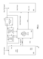
- FIG. 1 is a schematic block diagram depicting a system for transferring data from a host device to a slave device in accordance with an embodiment of the present invention
- FIG. 2 is a schematic block diagram depicting a busy signal generator in accordance with an embodiment of the present invention
- FIG. 3 is a schematic block diagram depicting a pending request signal generator in accordance with an embodiment of the present invention.
- FIG. 4 is a schematic block diagram depicting a slave request signal generator in accordance with an embodiment of the present invention.
- a system for transferring data from a host device to a slave device is provided.
- the host and slave devices operate on host and slave clock signals, respectively.
- the system includes a synchronizer circuit for synchronizing the slave clock signal with the host clock signal and generating a synchronized slave clock signal.
- a positive edge detector is connected to the synchronizer circuit for detecting and generating a positive edge of the synchronized slave clock signal.
- a busy signal generator is connected to the positive edge detector and the host device for generating a busy signal when a host request is being processed by the slave device.
- a slave request generation and data latch circuit is connected to the host device, the slave device, the positive edge detector, and the busy signal generator, for receiving and storing one or more host requests and host data, and generating and transmitting a slave request signal to the slave device.
- the slave request generation and data latch circuit generates and transmits the slave request signal when the busy signal is de-asserted and the positive edge of the synchronized slave clock signal is generated.
- a system for transferring data from a host device to a slave device is provided.
- the host and slave devices operate on host and slave clock signals, respectively.
- the system includes a synchronizer circuit for synchronizing the slave clock signal with the host clock signal and generating a synchronized slave clock signal.
- a positive edge detector is connected to the synchronizer circuit for detecting and generating a positive edge of the synchronized slave clock signal.
- a busy signal generator is connected to the positive edge detector and the host device, for generating a busy signal when a host request is being processed by the slave device.
- the busy signal generator includes first and second NOT gates for receiving slave and pending request signals and generating inverted slave and pending request signals, respectively.
- a first AND gate is connected to the first and second NOT gates, for receiving the inverted slave and inverted pending request signals, the busy signal, and a host request signal and generating a first intermediate signal.
- a second AND gate is provided for receiving the host and slave request signals, and the positive edge of synchronized slave clock signal and generating a second intermediate signal.
- a NOR gate is connected to the output terminals of the first and second AND gates, for receiving the first and second intermediate signals and generating a third intermediate signal.
- a first flip-flop has a data input terminal connected to the NOR gate for receiving the third intermediate signal, a clock input terminal that receives the host clock signal, and an output terminal that generates the busy signal. The output of the first flip-flop is connected to an input of the first AND gate.
- the system further includes a slave request generation and data latch circuit that is connected to the host and slave devices, the positive edge detector, and the busy signal generator, for receiving and storing one or more host requests and host data, and generating and transmitting a slave request signal to the slave device when the busy signal is de-asserted and the positive edge of the synchronized slave clock signal is generated.
- the slave request generation and data latch circuit includes a pending request signal generator for generating the pending request signal.
- the pending request signal generator includes third and fourth NOT gates, third through fifth AND gates, first through third multiplexers and a second flip-flop. The third NOT gate receives the busy signal and generates an inverted busy signal.
- the third AND gate is connected to the third NOT gate for receiving the inverted busy and host request signals and generating a fourth intermediate signal.
- the fourth AND gate receives the pending request signal and the positive edge of the synchronized slave clock signal and generates a fifth intermediate signal.
- the fourth NOT gate receives the busy signal and generates the inverted busy signal and the fifth AND gate receives the positive edge of synchronized slave clock signal and the inverted busy signal, and generates a sixth intermediate signal.
- the first multiplexer has a first input that receives logic one as a first input signal, a second input that receives the pending request signal, and a select input connected to the output of the third AND gate for receiving the fourth intermediate signal.
- the first multiplexer selectively provides one of the pending request and first input signals as a first mux output signal.
- the second multiplexer has a first input that receives logic zero as a second input signal, a second input that is connected to the output terminal of the first multiplexer for receiving the first mux output signal, and a select input connected to the output terminal of the fourth AND gate for receiving the fifth intermediate signal.
- the second multiplexer selectively provides one of the second input and first mux output signals as a second mux output signal.
- the third multiplexer has a first input that receives logic zero as a third input signal, a second input that is connected to the output terminal of the second multiplexer for receiving the second mux output signal, and a select input connected to the output terminal of the fifth AND gate for receiving the sixth intermediate signal.
- the third multiplexer selectively provides one of the third input and second mux output signals as a third mux output signal.
- the second flip-flop has a data input terminal connected to the output terminal of the third multiplexer for receiving the third mux output signal, a clock input terminal that receives the host clock signal, and an output terminal that provides the pending request signal.
- the output terminal of the second flip-flop is connected to the second input terminal of the first multiplexer.
- Various embodiments of the present invention provide a system for transferring data between host and slave devices of a system-on-chip (SoC) that operate at substantially different clock signal frequencies.
- the system includes a slave request generation and data latch circuit.
- the host device transmits a host request signal and host data to the slave request generation and data latch circuit for execution by the slave device.
- the slave request generation and data latch circuit stores the host data and transmits the host data to the slave device at a positive edge of a synchronized slave clock signal.
- the host device can perform other tasks when the slave device is executing the host request, thereby reducing the number of clock cycles of the host clock signal required by the host device, which increases the efficiency of the host device. Synchronizing the slave clock signal with the host clock signal eliminates the need for a handshake mechanism between the host and slave devices and reduces latency in data processing.
- FIG. 1 a schematic block diagram depicting a system 100 for transferring data from a host device 102 to a slave device 104 , in accordance with an embodiment of the present invention, is shown.
- the system 100 includes a busy signal generator 106 , a positive edge detector 108 , a synchronizer circuit 110 , and a slave request generation and data latch circuit 112 .
- the host device 102 generates a host request signal for transmitting host data to the slave device 104 .
- the host device 102 is a processor and the slave device 104 is a data register (not shown) and both of the host and slave devices 102 and 104 are a part of a system-on-chip (SoC, not shown).
- the host data includes programming instructions issued by the processor for programming the data register.
- the host device 102 operates on a host clock signal and the slave device 104 operates on a slave clock signal.
- the host clock signal has a higher frequency than the slave clock signal.
- the synchronizer circuit 110 synchronizes the frequency of the slave clock signal in a host clock domain (i.e., the host device 102 ) to generate a synchronized slave clock signal.
- the synchronizer circuit 110 receives the slave clock signal at an input terminal (D) and the host clock signal at a clock input terminal (CLK) and generates the host clock domain synchronized slave clock signal at an output terminal (Q).
- the synchronizer circuit 110 is well known in that art and may be formed using a pair of cascaded flip-flops (not shown).
- the synchronized slave clock signal is provided to the positive edge detector 108 that detects a positive edge of the synchronized slave clock signal which is provided to the busy signal generator 106 .
- the busy signal generator 106 also receives the host clock signal, a slave request signal, a pending request signal, and the host request signal and generates a busy signal.
- the busy signal is transmitted to the host device 102 and the slave request generation and data latch circuit 112 .
- the slave request generation and data latch circuit 112 may include a host data latch formed using one or more flip-flops (not shown) that store host data corresponding to one or more host requests that are transmitted to the slave device 104 for processing, based on the host request and busy signals.
- the slave request generation and data latch circuit 112 also includes a pending request signal generator (shown in FIG.
- the slave request generation and data latch circuit 112 further includes a slave request generator (shown in FIG. 4 ) that receives the positive edge of the synchronized slave clock signal, and the busy, host request, pending request, and host clock signals and generates the slave request signal.
- a slave request generator shown in FIG. 4
- the host device 102 Upon storing the host data, the host device 102 is not required to wait for the host request to be executed by the slave device 104 and can continue executing other priority tasks, thereby reducing the number of clock cycles required by the host device 102 .
- the pending request signal is driven to a logic high state based on the host request signal, the host clock signal, and the detection of the positive edge of the synchronized slave clock signal.
- the logic high state of the pending request signal indicates that a pending host request is queued for execution by the slave device 104 and the host data is pending to be transmitted to the slave device 104 .
- the slave request signal is generated based on the positive edge of the synchronized slave clock signal, and the busy, host request, pending request, and host clock signals.
- the slave request signal is driven to a logic high state upon detecting the positive edge of the synchronized slave clock signal, the host data is transmitted to the slave device 104 for processing.
- the busy signal generator 106 includes a first logic circuit 202 and a first flip-flop 204 .
- the first logic circuit 202 includes first and second NOT gates 206 and 208 , first and second AND gate 210 and 212 , and a NOR gate 214 .
- the first and second NOT gates 206 and 208 are connected to the first AND gate 210 .
- An output terminal of the first AND gate 210 is connected to a first input terminal of the NOR gate 214 and an output terminal of the second AND gate 212 is connected to a second input terminal of the NOR gate 214 .
- An output terminal of the NOR gate 214 is connected to an input terminal (D) of the first flip-flop 204 and an output terminal of the first flip-flop 204 is connected to the first AND gate 210 .
- the first and second NOT gates 206 and 208 receive the slave request and pending request signals and generate inverted slave request and inverted pending request signals, respectively, which are transmitted to the first AND gate 210 .
- the first AND gate 210 also receives the busy signal from the output terminal of the flip-flop 204 and the host request signal.
- the first AND gate 210 generates and transmits a first intermediate signal to the NOR gate 214 .
- the second AND gate 212 receives the host and slave request signals and the positive edge of the synchronized slave clock signals.
- the second AND gate 212 generates and transmits a second intermediate signal to the NOR gate 214 .
- the NOR gate 214 receives the first and second intermediate signals and generates and transmits a third intermediate signal to the input terminal of the first flip-flop 204 .
- the first flip-flop 204 also receives the host clock signal at a clock input terminal and generates the busy signal at the output terminal thereof.
- the pending request signal generator 300 is part of the slave request generation and data latch circuit 112 and includes a second and third logic circuits 302 and 304 , three muxes (first through third muxes) 306 - 310 , a second flip-flop 312 , and a third AND gate 314 .
- the second logic circuit 302 includes a third NOT gate 316 and a fourth AND gate 318 and the third logic circuit 304 includes a fourth NOT gate 320 and a fifth AND gate 322 .
- the third NOT gate 316 is connected to the fourth AND gate 318 and an output terminal of the fourth AND gate 318 is connected to a select input terminal of the first mux 306 .
- An output terminal of the third AND gate 314 is connected to a select input terminal of the second mux 308 and a second input terminal of the second mux 308 is connected to an output terminal of the first mux 306 .
- the fourth NOT gate 320 is connected to the fifth AND gate 322 and an output terminal of the fifth AND gate 322 is connected to a select input terminal of the third mux 310 .
- An output terminal of the second mux 308 is connected to a second input terminal of the third mux 310 and an output terminal of the third mux 310 is connected to an input terminal (D) of the second flip-flop 312 .
- An output terminal of the second flip-flop 312 is connected to a second input terminal of the first mux 306 .
- the second flip-flop 312 receives the host clock signal at a clock input terminal thereof.
- the third NOT gate 316 receives the busy signal and generates an inverted busy signal.
- the fourth AND gate 318 receives the host request signal and the inverted busy signal and generates a fourth intermediate signal.
- the fourth AND gate 318 transmits the fourth intermediate signal to the select input terminal of the first mux 306 .
- the first mux 306 receives logic one as a first input signal at a first input terminal thereof and the pending request signal at the second input terminal thereof and selectively provides at least one of the first input and pending request signals as a first output signal at the output terminal thereof.
- the first output signal is provided to the second input terminal of the second mux 308 .
- the second mux 308 receives logic zero as a second input signal at a first input terminal thereof.
- the third AND gate 314 receives the pending request signal and the positive edge of the synchronized slave clock signal and generates and transmits a fifth intermediate signal to the select input terminal of the second mux 308 .
- the second mux 308 selectively provides at least one of the second input and first output signals as a second output signal at an output terminal thereof.
- the second output signal is provided to the second input terminal of the third mux 310 .
- logic zero is provided as a third input signal at a first input terminal of the third mux 310 .
- the fourth NOT gate 320 receives the busy signal and generates the inverted busy signal and transmits the inverted busy signal to the fifth AND gate 322 .
- the fifth AND gate 322 also receives the positive edge of the synchronized slave clock signal and generates and transmits a sixth intermediate signal to a select input terminal of the third mux 310 .
- the third mux 310 selectively provides at least one of the third input and second output signals at an output terminal thereof as a third output signal.
- the third mux 310 transmits the third output signal to the input terminal D of the second flip-flop 312 .
- the second flip-flop 312 generates the pending request signal based on the third output signal and the host clock signal.
- the slave request signal generator 400 is also a part of the slave request generation and data latch circuit 112 and includes four muxes (fourth through seventh muxes) 402 - 408 , a third flip-flop 410 , three logic circuits (fourth through sixth logic circuits) 412 - 416 , and a sixth AND gate 418 .
- the fourth logic circuit 412 includes a fifth NOT gate 420 and a seventh AND gate 422 .
- the fifth logic circuit 414 includes a sixth NOT gate 424 , an eighth AND gate 426 , and a seventh NOT gate 428 .
- the sixth logic circuit 416 includes an eighth NOT gate 430 and a ninth AND gate 432 .
- the fifth NOT gate 420 is connected to the seventh AND gate 422 and an output terminal of the seventh AND gate 422 is connected to a select input terminal of the fifth mux 404 .
- a second input terminal of the fifth mux 404 is connected to an output terminal of the fourth mux 402 .
- the sixth NOT gate 424 is connected to the eighth AND gate 426 and an output terminal of the eighth AND gate 426 is connected to the seventh NOT gate 428 .
- the seventh NOT gate 428 is connected to a first input terminal of the sixth mux 406 and a second input terminal of the sixth mux 406 is connected to an output terminal of the fifth mux 404 .
- An output terminal of the sixth AND gate 418 is connected to a select input terminal of the sixth mux 406 .
- a second input terminal of the seventh mux 408 is connected to an output terminal of the sixth mux 406 .
- the eighth NOT gate 430 is connected to the ninth AND gate 432 and an output terminal of the ninth AND gate 432 is connected to a select input terminal of the seventh mux 408 .
- An output terminal of the seventh mux 408 is connected to an input terminal (D) of the third flip-flop 410 and an output terminal of the third flip-flop 410 is connected to a second input terminal of the fourth mux 402 .
- the fourth mux 402 receives the positive edge of the synchronized slave clock signal at a select input terminal thereof and logic zero as a fourth input signal at a first input terminal and the slave request signal at the second input terminal thereof.
- the fourth mux 402 selectively provides at least one of the fourth input and slave request signals at the output terminal thereof as a fourth output signal.
- the fifth NOT gate 420 receives the pending request signal and generates and transmits an inverted pending request signal to the seventh AND gate 422 .
- the seventh AND gate 422 also receives the positive edge of the synchronized slave clock signal, the host request signal, and the inverted pending request signal and generates a seventh intermediate signal at an output terminal thereof.
- the seventh AND gate 422 provides the seventh intermediate signal to the select input terminal of the fifth mux 404 .
- the fifth mux 404 receives logic one as a fifth input signal at a first input terminal and the fourth output signal at the second input terminal and selectively provides at least one of the fifth input and fourth output signals as a fifth output signal at the output terminal thereof.
- the sixth NOT gate 424 receives the host request signal and generates and transmits an inverted host request signal to the eighth AND gate 426 .
- the eighth AND gate 426 also receives the slave request signal and generates an eighth intermediate signal at an output terminal thereof and transmits the eighth intermediate signal to the seventh NOT gate 428 .
- the seventh NOT gate 428 generates and transmits an inverted eighth intermediate signal to a first input terminal of the sixth mux 406 .
- the sixth mux 406 receives the fifth output signal at the second input terminal thereof.
- the sixth AND gate 418 receives the pending request signal and the positive edge of the synchronized slave clock signal to generate and transmit a ninth intermediate signal to the select input terminal of the sixth mux 406 .
- the sixth mux 406 selectively provides at least one of the fifth output signal and the inverted eighth intermediate signal at an output terminal thereof as a sixth output signal.
- the sixth mux 406 transmits the sixth output signal to the second input terminal of the seventh mux 408 .
- the seventh mux 408 also receives logic one as a sixth input signal at a first input terminal thereof.
- the eighth NOT gate 430 receives the busy signal and generates and transmits the inverted busy signal to the ninth AND gate 432 .
- the ninth AND gate 432 also receives the positive edge of the synchronized slave clock signal and generates and transmits a tenth intermediate signal to the select input terminal of the seventh mux 408 .
- the seventh mux 408 selectively provides at least one of the sixth input and sixth output signals at the output terminal as a seventh output signal.
- the seventh mux 408 transmits the seventh output signal to the input terminal D of the third flip-flop 410 .
- the third flip-flop 410 receives the host clock signal at a clock input terminal thereof.
- the third flip-flop 410 generates the slave request signal at the output terminal.
Landscapes
- Engineering & Computer Science (AREA)
- Theoretical Computer Science (AREA)
- Physics & Mathematics (AREA)
- General Engineering & Computer Science (AREA)
- General Physics & Mathematics (AREA)
- Information Transfer Systems (AREA)
Abstract
Description
Claims (20)
Priority Applications (1)
| Application Number | Priority Date | Filing Date | Title |
|---|---|---|---|
| US13/682,755 US8977882B2 (en) | 2012-11-21 | 2012-11-21 | System for data transfer between asynchronous clock domains |
Applications Claiming Priority (1)
| Application Number | Priority Date | Filing Date | Title |
|---|---|---|---|
| US13/682,755 US8977882B2 (en) | 2012-11-21 | 2012-11-21 | System for data transfer between asynchronous clock domains |
Publications (2)
| Publication Number | Publication Date |
|---|---|
| US20140143581A1 US20140143581A1 (en) | 2014-05-22 |
| US8977882B2 true US8977882B2 (en) | 2015-03-10 |
Family
ID=50729118
Family Applications (1)
| Application Number | Title | Priority Date | Filing Date |
|---|---|---|---|
| US13/682,755 Active 2033-11-30 US8977882B2 (en) | 2012-11-21 | 2012-11-21 | System for data transfer between asynchronous clock domains |
Country Status (1)
| Country | Link |
|---|---|
| US (1) | US8977882B2 (en) |
Cited By (4)
| Publication number | Priority date | Publication date | Assignee | Title |
|---|---|---|---|---|
| EP4075289A1 (en) * | 2021-04-15 | 2022-10-19 | Nordic Semiconductor ASA | Handshake circuits |
| US11855633B2 (en) | 2022-05-27 | 2023-12-26 | Stmicroelectronics (Rousset) Sas | Programmable logic array with reliable timing |
| US11942935B2 (en) | 2022-07-08 | 2024-03-26 | Stmicroelectronics (Rousset) Sas | Programmable logic block with multiple types of programmable arrays and flexible clock selection |
| US11979153B2 (en) | 2022-04-29 | 2024-05-07 | Stmicroelectronics (Rousset) Sas | Input signal shaping for a programmable logic array |
Families Citing this family (5)
| Publication number | Priority date | Publication date | Assignee | Title |
|---|---|---|---|---|
| US20140281652A1 (en) * | 2013-03-14 | 2014-09-18 | Nvidia Corporation | Data synchronization across asynchronous boundaries using selectable synchronizers to minimize latency |
| US10191944B2 (en) * | 2015-10-23 | 2019-01-29 | Oracle International Corporation | Columnar data arrangement for semi-structured data |
| US10915485B2 (en) | 2019-05-17 | 2021-02-09 | Nxp Usa, Inc. | Circuit for asynchronous data transfer |
| CN111324562B (en) * | 2020-02-16 | 2021-08-06 | 苏州浪潮智能科技有限公司 | Clock domain crossing system of AHB and working method |
| CN113760860B (en) * | 2020-11-12 | 2023-09-22 | 北京京东振世信息技术有限公司 | Data reading method and device |
Citations (6)
| Publication number | Priority date | Publication date | Assignee | Title |
|---|---|---|---|---|
| US6377650B1 (en) | 1999-08-26 | 2002-04-23 | Texas Instruments Incorporated | Counter register monitor and update circuit for dual-clock system |
| US6499080B1 (en) | 1999-01-19 | 2002-12-24 | Texas Instruments Incorporated | Post write buffer for a dual clock system |
| US20040243869A1 (en) | 2003-05-30 | 2004-12-02 | Sun Microsystems, Inc. | Synchronous data transfer across clock domains |
| US20050116783A1 (en) * | 2003-05-09 | 2005-06-02 | Adkisson Richard W. | Phase detector for a programmable clock synchronizer |
| US20070280396A1 (en) * | 2006-05-31 | 2007-12-06 | Broadcom Corporation | Method and system for advance high performance bus synchronizer |
| US20090261869A1 (en) * | 2008-04-16 | 2009-10-22 | Advanced Micro Devices, Inc. | Clock domain data transfer device and methods thereof |
-
2012
- 2012-11-21 US US13/682,755 patent/US8977882B2/en active Active
Patent Citations (6)
| Publication number | Priority date | Publication date | Assignee | Title |
|---|---|---|---|---|
| US6499080B1 (en) | 1999-01-19 | 2002-12-24 | Texas Instruments Incorporated | Post write buffer for a dual clock system |
| US6377650B1 (en) | 1999-08-26 | 2002-04-23 | Texas Instruments Incorporated | Counter register monitor and update circuit for dual-clock system |
| US20050116783A1 (en) * | 2003-05-09 | 2005-06-02 | Adkisson Richard W. | Phase detector for a programmable clock synchronizer |
| US20040243869A1 (en) | 2003-05-30 | 2004-12-02 | Sun Microsystems, Inc. | Synchronous data transfer across clock domains |
| US20070280396A1 (en) * | 2006-05-31 | 2007-12-06 | Broadcom Corporation | Method and system for advance high performance bus synchronizer |
| US20090261869A1 (en) * | 2008-04-16 | 2009-10-22 | Advanced Micro Devices, Inc. | Clock domain data transfer device and methods thereof |
Non-Patent Citations (2)
| Title |
|---|
| Sathe, V., Papaefthymiou, M. C., Kosonocky, S. V., and Kim, S., On-chip Synchronous Communication Between Clock Domains with Quotient Frequencies, Electronics Letters, vol. 43, No. 9, pp. 497-498, Apr. 26, 2007. |
| Simon Moore, George Taylor, Bob Mullins and Peter Robinson, Channel Communication Between Independent Clock Domains, First ACiD-WG Workshop of the European Commission's Fifth Framework Programme, 2001. |
Cited By (6)
| Publication number | Priority date | Publication date | Assignee | Title |
|---|---|---|---|---|
| EP4075289A1 (en) * | 2021-04-15 | 2022-10-19 | Nordic Semiconductor ASA | Handshake circuits |
| US20220335168A1 (en) * | 2021-04-15 | 2022-10-20 | Nordic Semiconductor Asa | Handshake circuits |
| US12118133B2 (en) * | 2021-04-15 | 2024-10-15 | Nordic Semiconductor Asa | Handshake circuits |
| US11979153B2 (en) | 2022-04-29 | 2024-05-07 | Stmicroelectronics (Rousset) Sas | Input signal shaping for a programmable logic array |
| US11855633B2 (en) | 2022-05-27 | 2023-12-26 | Stmicroelectronics (Rousset) Sas | Programmable logic array with reliable timing |
| US11942935B2 (en) | 2022-07-08 | 2024-03-26 | Stmicroelectronics (Rousset) Sas | Programmable logic block with multiple types of programmable arrays and flexible clock selection |
Also Published As
| Publication number | Publication date |
|---|---|
| US20140143581A1 (en) | 2014-05-22 |
Similar Documents
| Publication | Publication Date | Title |
|---|---|---|
| US8977882B2 (en) | System for data transfer between asynchronous clock domains | |
| US8352774B2 (en) | Inter-clock domain data transfer FIFO circuit | |
| US8275977B2 (en) | Debug signaling in a multiple processor data processing system | |
| US8626979B2 (en) | Common protocol engine interface for a controller interface | |
| JP2002523857A (en) | FIFO using asynchronous logic | |
| US8570069B2 (en) | Clock gating cell circuit | |
| TW200830108A (en) | Two-cycle return path clocking | |
| US11567893B2 (en) | Method and a mirrored serial interface (MSI) for transferring data | |
| US9071256B1 (en) | Method for link resets in a SerDes system | |
| US8559576B2 (en) | Adaptive synchronization circuit | |
| US7234017B2 (en) | Computer system architecture for a processor connected to a high speed bus transceiver | |
| Fenwick et al. | The AlphaServer 8000 series: High-end server platform development | |
| US9940288B1 (en) | SerDes alignment process | |
| US7444448B2 (en) | Data bus mechanism for dynamic source synchronized sampling adjust | |
| US20100315134A1 (en) | Systems and methods for multi-lane communication busses | |
| US8780935B2 (en) | Communication system, and corresponding integrated circuit and method | |
| US6067629A (en) | Apparatus and method for pseudo-synchronous communication between clocks of different frequencies | |
| WO2014127674A1 (en) | Method and device for transmitting bus data signal, supporting dvfs | |
| EP3739463B1 (en) | Circuit for asynchronous data transfer | |
| EP3173895B1 (en) | Clock tree implementation method, system-on-chip and computer storage medium | |
| GB2521035A (en) | A synchronous bridge circuitry and a method of transferring data using asynchronous bridge circuitry | |
| CN208190652U (en) | A kind of mainboard of full duplex Universal Synchronous Asynchronous serial transceiver | |
| US8370543B1 (en) | Busy detection logic for asynchronous communication port | |
| US6377581B1 (en) | Optimized CPU-memory high bandwidth multibus structure simultaneously supporting design reusable blocks | |
| US8599982B2 (en) | Interface system, and corresponding integrated circuit and method |
Legal Events
| Date | Code | Title | Description |
|---|---|---|---|
| AS | Assignment |
Owner name: FREESCALE SEMICONDUCTOR, INC., TEXAS Free format text: ASSIGNMENT OF ASSIGNORS INTEREST;ASSIGNORS:GARG, SANDEEP;IQBAL, ASIF;KAPOOR, RAJAN;SIGNING DATES FROM 20121101 TO 20121121;REEL/FRAME:029333/0990 |
|
| AS | Assignment |
Owner name: CITIBANK, N.A., AS NOTES COLLATERAL AGENT, NEW YOR Free format text: SUPPLEMENT TO IP SECURITY AGREEMENT;ASSIGNOR:FREESCALE SEMICONDUCTOR, INC.;REEL/FRAME:030258/0558 Effective date: 20130214 Owner name: CITIBANK, N.A., AS NOTES COLLATERAL AGENT, NEW YOR Free format text: SUPPLEMENT TO IP SECURITY AGREEMENT;ASSIGNOR:FREESCALE SEMICONDUCTOR, INC.;REEL/FRAME:030258/0523 Effective date: 20130214 Owner name: CITIBANK, N.A., AS COLLATERAL AGENT, NEW YORK Free format text: SUPPLEMENT TO IP SECURITY AGREEMENT;ASSIGNOR:FREESCALE SEMICONDUCTOR, INC.;REEL/FRAME:030258/0540 Effective date: 20130214 |
|
| AS | Assignment |
Owner name: CITIBANK, N.A., AS NOTES COLLATERAL AGENT, NEW YOR Free format text: SECURITY AGREEMENT;ASSIGNOR:FREESCALE SEMICONDUCTOR, INC.;REEL/FRAME:030633/0424 Effective date: 20130521 |
|
| AS | Assignment |
Owner name: CITIBANK, N.A., AS NOTES COLLATERAL AGENT, NEW YOR Free format text: SECURITY AGREEMENT;ASSIGNOR:FREESCALE SEMICONDUCTOR, INC.;REEL/FRAME:031591/0266 Effective date: 20131101 |
|
| STCF | Information on status: patent grant |
Free format text: PATENTED CASE |
|
| AS | Assignment |
Owner name: FREESCALE SEMICONDUCTOR, INC., TEXAS Free format text: PATENT RELEASE;ASSIGNOR:CITIBANK, N.A., AS COLLATERAL AGENT;REEL/FRAME:037357/0671 Effective date: 20151207 Owner name: FREESCALE SEMICONDUCTOR, INC., TEXAS Free format text: PATENT RELEASE;ASSIGNOR:CITIBANK, N.A., AS COLLATERAL AGENT;REEL/FRAME:037357/0685 Effective date: 20151207 |
|
| AS | Assignment |
Owner name: MORGAN STANLEY SENIOR FUNDING, INC., MARYLAND Free format text: ASSIGNMENT AND ASSUMPTION OF SECURITY INTEREST IN PATENTS;ASSIGNOR:CITIBANK, N.A.;REEL/FRAME:037486/0517 Effective date: 20151207 |
|
| AS | Assignment |
Owner name: MORGAN STANLEY SENIOR FUNDING, INC., MARYLAND Free format text: ASSIGNMENT AND ASSUMPTION OF SECURITY INTEREST IN PATENTS;ASSIGNOR:CITIBANK, N.A.;REEL/FRAME:037518/0292 Effective date: 20151207 |
|
| AS | Assignment |
Owner name: FREESCALE SEMICONDUCTOR, INC., TEXAS Free format text: PATENT RELEASE;ASSIGNOR:CITIBANK, N.A., AS COLLATERAL AGENT;REEL/FRAME:037494/0312 Effective date: 20151207 |
|
| AS | Assignment |
Owner name: MORGAN STANLEY SENIOR FUNDING, INC., MARYLAND Free format text: SUPPLEMENT TO THE SECURITY AGREEMENT;ASSIGNOR:FREESCALE SEMICONDUCTOR, INC.;REEL/FRAME:039138/0001 Effective date: 20160525 |
|
| AS | Assignment |
Owner name: NXP, B.V., F/K/A FREESCALE SEMICONDUCTOR, INC., NETHERLANDS Free format text: RELEASE BY SECURED PARTY;ASSIGNOR:MORGAN STANLEY SENIOR FUNDING, INC.;REEL/FRAME:040925/0001 Effective date: 20160912 Owner name: NXP, B.V., F/K/A FREESCALE SEMICONDUCTOR, INC., NE Free format text: RELEASE BY SECURED PARTY;ASSIGNOR:MORGAN STANLEY SENIOR FUNDING, INC.;REEL/FRAME:040925/0001 Effective date: 20160912 |
|
| AS | Assignment |
Owner name: NXP B.V., NETHERLANDS Free format text: RELEASE BY SECURED PARTY;ASSIGNOR:MORGAN STANLEY SENIOR FUNDING, INC.;REEL/FRAME:040928/0001 Effective date: 20160622 |
|
| AS | Assignment |
Owner name: NXP USA, INC., TEXAS Free format text: CHANGE OF NAME;ASSIGNOR:FREESCALE SEMICONDUCTOR, INC.;REEL/FRAME:040652/0241 Effective date: 20161107 Owner name: NXP USA, INC., TEXAS Free format text: MERGER;ASSIGNOR:FREESCALE SEMICONDUCTOR, INC.;REEL/FRAME:040652/0241 Effective date: 20161107 |
|
| AS | Assignment |
Owner name: NXP USA, INC., TEXAS Free format text: CORRECTIVE ASSIGNMENT TO CORRECT THE NATURE OF CONVEYANCE PREVIOUSLY RECORDED AT REEL: 040652 FRAME: 0241. ASSIGNOR(S) HEREBY CONFIRMS THE MERGER AND CHANGE OF NAME;ASSIGNOR:FREESCALE SEMICONDUCTOR, INC.;REEL/FRAME:041260/0850 Effective date: 20161107 |
|
| AS | Assignment |
Owner name: MORGAN STANLEY SENIOR FUNDING, INC., MARYLAND Free format text: CORRECTIVE ASSIGNMENT TO CORRECT THE REMOVE PATENTS 8108266 AND 8062324 AND REPLACE THEM WITH 6108266 AND 8060324 PREVIOUSLY RECORDED ON REEL 037518 FRAME 0292. ASSIGNOR(S) HEREBY CONFIRMS THE ASSIGNMENT AND ASSUMPTION OF SECURITY INTEREST IN PATENTS;ASSIGNOR:CITIBANK, N.A.;REEL/FRAME:041703/0536 Effective date: 20151207 |
|
| MAFP | Maintenance fee payment |
Free format text: PAYMENT OF MAINTENANCE FEE, 4TH YEAR, LARGE ENTITY (ORIGINAL EVENT CODE: M1551) Year of fee payment: 4 |
|
| AS | Assignment |
Owner name: SHENZHEN XINGUODU TECHNOLOGY CO., LTD., CHINA Free format text: CORRECTIVE ASSIGNMENT TO CORRECT THE TO CORRECT THE APPLICATION NO. FROM 13,883,290 TO 13,833,290 PREVIOUSLY RECORDED ON REEL 041703 FRAME 0536. ASSIGNOR(S) HEREBY CONFIRMS THE THE ASSIGNMENT AND ASSUMPTION OF SECURITYINTEREST IN PATENTS.;ASSIGNOR:MORGAN STANLEY SENIOR FUNDING, INC.;REEL/FRAME:048734/0001 Effective date: 20190217 |
|
| AS | Assignment |
Owner name: NXP B.V., NETHERLANDS Free format text: RELEASE BY SECURED PARTY;ASSIGNOR:MORGAN STANLEY SENIOR FUNDING, INC.;REEL/FRAME:050744/0097 Effective date: 20190903 |
|
| AS | Assignment |
Owner name: MORGAN STANLEY SENIOR FUNDING, INC., MARYLAND Free format text: CORRECTIVE ASSIGNMENT TO CORRECT THE REMOVE APPLICATION11759915 AND REPLACE IT WITH APPLICATION 11759935 PREVIOUSLY RECORDED ON REEL 037486 FRAME 0517. ASSIGNOR(S) HEREBY CONFIRMS THE ASSIGNMENT AND ASSUMPTION OF SECURITYINTEREST IN PATENTS;ASSIGNOR:CITIBANK, N.A.;REEL/FRAME:053547/0421 Effective date: 20151207 |
|
| AS | Assignment |
Owner name: NXP B.V., NETHERLANDS Free format text: CORRECTIVE ASSIGNMENT TO CORRECT THE REMOVEAPPLICATION 11759915 AND REPLACE IT WITH APPLICATION11759935 PREVIOUSLY RECORDED ON REEL 040928 FRAME 0001. ASSIGNOR(S) HEREBY CONFIRMS THE RELEASE OF SECURITYINTEREST;ASSIGNOR:MORGAN STANLEY SENIOR FUNDING, INC.;REEL/FRAME:052915/0001 Effective date: 20160622 |
|
| AS | Assignment |
Owner name: NXP, B.V. F/K/A FREESCALE SEMICONDUCTOR, INC., NETHERLANDS Free format text: CORRECTIVE ASSIGNMENT TO CORRECT THE REMOVEAPPLICATION 11759915 AND REPLACE IT WITH APPLICATION11759935 PREVIOUSLY RECORDED ON REEL 040925 FRAME 0001. ASSIGNOR(S) HEREBY CONFIRMS THE RELEASE OF SECURITYINTEREST;ASSIGNOR:MORGAN STANLEY SENIOR FUNDING, INC.;REEL/FRAME:052917/0001 Effective date: 20160912 |
|
| MAFP | Maintenance fee payment |
Free format text: PAYMENT OF MAINTENANCE FEE, 8TH YEAR, LARGE ENTITY (ORIGINAL EVENT CODE: M1552); ENTITY STATUS OF PATENT OWNER: LARGE ENTITY Year of fee payment: 8 |