US8765491B2 - Shallow trench isolation recess repair using spacer formation process - Google Patents
Shallow trench isolation recess repair using spacer formation process Download PDFInfo
- Publication number
- US8765491B2 US8765491B2 US12/914,095 US91409510A US8765491B2 US 8765491 B2 US8765491 B2 US 8765491B2 US 91409510 A US91409510 A US 91409510A US 8765491 B2 US8765491 B2 US 8765491B2
- Authority
- US
- United States
- Prior art keywords
- spacer layer
- gate structures
- transistor gate
- sti
- regions
- Prior art date
- Legal status (The legal status is an assumption and is not a legal conclusion. Google has not performed a legal analysis and makes no representation as to the accuracy of the status listed.)
- Expired - Fee Related, expires
Links
- 125000006850 spacer group Chemical group 0.000 title claims abstract description 61
- 238000000034 method Methods 0.000 title claims abstract description 27
- 238000002955 isolation Methods 0.000 title claims abstract description 14
- 230000015572 biosynthetic process Effects 0.000 title claims description 21
- 239000004065 semiconductor Substances 0.000 claims abstract description 25
- 239000000463 material Substances 0.000 claims abstract description 16
- 239000000758 substrate Substances 0.000 claims abstract description 10
- 230000008021 deposition Effects 0.000 claims abstract description 5
- 150000004767 nitrides Chemical class 0.000 claims description 35
- 229910021332 silicide Inorganic materials 0.000 claims description 14
- FVBUAEGBCNSCDD-UHFFFAOYSA-N silicide(4-) Chemical compound [Si-4] FVBUAEGBCNSCDD-UHFFFAOYSA-N 0.000 claims description 14
- 230000000873 masking effect Effects 0.000 claims description 4
- 239000010410 layer Substances 0.000 description 56
- 239000011800 void material Substances 0.000 description 9
- 238000004140 cleaning Methods 0.000 description 5
- 238000001878 scanning electron micrograph Methods 0.000 description 4
- 229910052751 metal Inorganic materials 0.000 description 3
- 239000002184 metal Substances 0.000 description 3
- 238000012876 topography Methods 0.000 description 3
- 229910052581 Si3N4 Inorganic materials 0.000 description 2
- 230000002265 prevention Effects 0.000 description 2
- 230000000295 complement effect Effects 0.000 description 1
- 230000007547 defect Effects 0.000 description 1
- 230000000694 effects Effects 0.000 description 1
- 238000005530 etching Methods 0.000 description 1
- 230000005669 field effect Effects 0.000 description 1
- 239000012212 insulator Substances 0.000 description 1
- 150000002500 ions Chemical class 0.000 description 1
- 238000004519 manufacturing process Methods 0.000 description 1
- 238000012986 modification Methods 0.000 description 1
- 230000004048 modification Effects 0.000 description 1
- 238000000059 patterning Methods 0.000 description 1
- 238000000206 photolithography Methods 0.000 description 1
- 229920002120 photoresistant polymer Polymers 0.000 description 1
- 238000005498 polishing Methods 0.000 description 1
- 239000011241 protective layer Substances 0.000 description 1
- HQVNEWCFYHHQES-UHFFFAOYSA-N silicon nitride Chemical compound N12[Si]34N5[Si]62N3[Si]51N64 HQVNEWCFYHHQES-UHFFFAOYSA-N 0.000 description 1
- 239000000126 substance Substances 0.000 description 1
- WFKWXMTUELFFGS-UHFFFAOYSA-N tungsten Chemical compound [W] WFKWXMTUELFFGS-UHFFFAOYSA-N 0.000 description 1
- 229910052721 tungsten Inorganic materials 0.000 description 1
- 239000010937 tungsten Substances 0.000 description 1
Images


Classifications
-
- H—ELECTRICITY
- H10—SEMICONDUCTOR DEVICES; ELECTRIC SOLID-STATE DEVICES NOT OTHERWISE PROVIDED FOR
- H10D—INORGANIC ELECTRIC SEMICONDUCTOR DEVICES
- H10D84/00—Integrated devices formed in or on semiconductor substrates that comprise only semiconducting layers, e.g. on Si wafers or on GaAs-on-Si wafers
- H10D84/01—Manufacture or treatment
- H10D84/0123—Integrating together multiple components covered by H10D12/00 or H10D30/00, e.g. integrating multiple IGBTs
- H10D84/0126—Integrating together multiple components covered by H10D12/00 or H10D30/00, e.g. integrating multiple IGBTs the components including insulated gates, e.g. IGFETs
- H10D84/0147—Manufacturing their gate sidewall spacers
-
- H—ELECTRICITY
- H10—SEMICONDUCTOR DEVICES; ELECTRIC SOLID-STATE DEVICES NOT OTHERWISE PROVIDED FOR
- H10D—INORGANIC ELECTRIC SEMICONDUCTOR DEVICES
- H10D84/00—Integrated devices formed in or on semiconductor substrates that comprise only semiconducting layers, e.g. on Si wafers or on GaAs-on-Si wafers
- H10D84/01—Manufacture or treatment
- H10D84/0123—Integrating together multiple components covered by H10D12/00 or H10D30/00, e.g. integrating multiple IGBTs
- H10D84/0126—Integrating together multiple components covered by H10D12/00 or H10D30/00, e.g. integrating multiple IGBTs the components including insulated gates, e.g. IGFETs
- H10D84/0151—Manufacturing their isolation regions
-
- H—ELECTRICITY
- H10—SEMICONDUCTOR DEVICES; ELECTRIC SOLID-STATE DEVICES NOT OTHERWISE PROVIDED FOR
- H10D—INORGANIC ELECTRIC SEMICONDUCTOR DEVICES
- H10D84/00—Integrated devices formed in or on semiconductor substrates that comprise only semiconducting layers, e.g. on Si wafers or on GaAs-on-Si wafers
- H10D84/01—Manufacture or treatment
- H10D84/02—Manufacture or treatment characterised by using material-based technologies
- H10D84/03—Manufacture or treatment characterised by using material-based technologies using Group IV technology, e.g. silicon technology or silicon-carbide [SiC] technology
- H10D84/038—Manufacture or treatment characterised by using material-based technologies using Group IV technology, e.g. silicon technology or silicon-carbide [SiC] technology using silicon technology, e.g. SiGe
-
- H—ELECTRICITY
- H01—ELECTRIC ELEMENTS
- H01L—SEMICONDUCTOR DEVICES NOT COVERED BY CLASS H10
- H01L21/00—Processes or apparatus adapted for the manufacture or treatment of semiconductor or solid state devices or of parts thereof
- H01L21/70—Manufacture or treatment of devices consisting of a plurality of solid state components formed in or on a common substrate or of parts thereof; Manufacture of integrated circuit devices or of parts thereof
- H01L21/71—Manufacture of specific parts of devices defined in group H01L21/70
- H01L21/76—Making of isolation regions between components
- H01L21/762—Dielectric regions, e.g. EPIC dielectric isolation, LOCOS; Trench refilling techniques, SOI technology, use of channel stoppers
- H01L21/76224—Dielectric regions, e.g. EPIC dielectric isolation, LOCOS; Trench refilling techniques, SOI technology, use of channel stoppers using trench refilling with dielectric materials
Definitions
- the present invention relates generally to semiconductor device manufacturing and, more particularly, to a structure and method for shallow trench isolation (STI) recess repair prior to silicide processing, using a gate spacer layer.
- STI shallow trench isolation
- certain inactive areas of a semiconductor device defined by STI regions may also have so called “dummy” gate structures formed thereon.
- These dummy gate structures on the STI regions are electrically non-functional, but serve one or more mechanical purposes.
- substantially planar surfaces within a semiconductor topography may play an important role in fabricating overlying layers and structures. That is, step coverage problems may arise when a material is deposited over a surface having raised and recessed regions. Step coverage is defined as a measure of how well a film conforms over an underlying step and is expressed by the ratio of the minimum thickness of a film as it crosses a step to the nominal thickness of the film over horizontal regions.
- correctly patterning layers upon a surface containing fluctuations in elevation may be difficult using optical lithography.
- An STI recess therefore introduces a significant challenge for a middle-of-the-line (MOL) nitride layer to fill the gap between adjacent gates, especially at sub-32 nanometer (nm) ground rules.
- MOL middle-of-the-line
- An incomplete gap fill also known as a tungsten (W) subway void defect, remains a yield and reliability concern, even on electrically non-functional STI regions.
- a method of forming a semiconductor device includes forming a spacer layer over a plurality of transistor gate structures, the transistor gate structures being formed over both active and shallow trench isolation (STI) regions of a substrate; and subjecting the spacer layer to a directional etch so as to form sidewall spacers adjacent the plurality of transistor gate structures, and wherein a horizontal fill portion of the spacer remains in one more recesses present in the STI region so as to substantially planarize the STI regions prior to subsequent material deposition thereon.
- STI shallow trench isolation
- a method of forming a semiconductor device includes forming a nitride spacer layer over a plurality of transistor gate structures, the transistor gate structures being formed over both active and shallow trench isolation (STI) regions of a substrate; masking the nitride spacer layer so as to protect portions of the nitride spacer layer over the STI regions; and subjecting exposed portions of the nitride spacer layer over the active regions to a directional etch so as to form nitride sidewall spacers adjacent the plurality of transistor gate structures; wherein the nitride spacer layer is formed at an initial thickness sufficient to both facilitate sidewall spacer formation in the active area and to prevent pinch off of the spacer layer at locations corresponding to one or more recesses present in the STI regions.
- STI shallow trench isolation
- FIGS. 2( a ) through 2 ( c ) are a series of cross sectional views illustrating a method of STI recess repair prior to silicide processing, in accordance with an exemplary embodiment of the invention, in which:
- FIG. 2( a ) illustrates a plurality of transistors formed on active and STI regions of a semiconductor device, wherein a portion of the STI region between adjacent transistor gates has a recess formed therein;
- FIG. 2( c ) illustrates selective removal of portions of the nitride spacer layer of FIG. 2( b ) so as to form sidewall spacers on the gate structure and to fill the STI region recess;
- FIG. 4( b ) illustrates the formation of a nitride spacer layer over the structure of FIG. 4( a );
- FIG. 4( c ) illustrates masking of the semiconductor device so as to expose the active region
- FIG. 4( d ) illustrates selective removal of portions of the nitride spacer layer in the active regions of FIG. 4( c ) remains to serve as a capping layer for the STI region gate structures.
- a structure and method for STI recess repair prior to silicide processing using a gate spacer layer.
- a gate spacer layer e.g., a nitride
- portions of the gate spacer layer between adjacent gates on STI layers can be selectively removed so as to both (1) fill in the STI recess caused by cleaning processes and (2) form sidewall spacers on the gate structures. This in turn prevents voids from being formed in post-silicidation cap layers formed over the gate structures.
- FIG. 1 there is shown an SEM image of a conventionally formed semiconductor device 100 having gate structures 102 formed on an STI region 104 of the device 100 .
- a nitride cap layer 106 is pinched between adjacent gate structures 102 so as result in a void 108 that is not filled by the overlying interlevel dielectric (ILD) layer (e.g., oxide) 110 atop the nitride cap layer 106 .
- ILD interlevel dielectric
- the void 108 is present as a result of the STI recess 112 formed during cleaning processes in FEOL, which recess 112 exacerbated by a metal silicide process in forming silicide contacts 114 .
- FIGS. 2( a ) through 2 ( c ) are a series of cross sectional views illustrating a method of STI recess repair prior to silicide processing, in accordance with an exemplary embodiment of the invention.
- a semiconductor device 200 includes an active area 202 and an STI area 204 , both of which have transistor gate structures 206 formed thereon.
- transistor gate structures 206 formed thereon.
- a portion of the STI region 204 between adjacent transistor gates 206 has a recess 208 formed therein.
- a nitride layer 210 such as a silicon nitride layer (Si 3 N 4 ) is formed over the entire structure.
- the nitride layer deposition conditions are selected so as to result in a layer thickness that is sufficient to fill in the recess 208 , and to allow for a gate sidewall spacer formation following a directional etch, but also thin enough so as to prevent a pinching off of the layer above the recess 208 in the STI region 204 , as particularly shown in FIG. 2( b ).
- the thickness of the nitride layer 210 should, at most, be slightly less than half the distance between adjacent gate structures in the STI region.
- nitride layer 210 comes to being pinched off above the recess, the more nitride material will be left in the recess following etching. However, if the nitride layer 210 is completely pinched off, this will prevent desired sidewall spacer formation.
- the nitride layer 210 is then subjected to an anisotropic (directional) reactive ion etch (RIE) that results in the formation of nitride sidewall spacers 212 adjacent the gate structures 206 in both the active region 202 and the STI region.
- RIE reactive ion etch
- a horizontal fill portion 214 of nitride material remains in the STI recess so as to substantially planarize the STI region 204 . In so doing, the subsequent formation of a nitride cap layer post-silicidation is prevented from the type of void formation discussed above.
- FIG. 3 is an SEM image of a resulting structure using the exemplary method of FIGS. 2( a ) through 2 ( c ), illustrating the prevention of a void formed in the nitride cap layer.
- the horizontal fill portion 214 of nitride fill material substantially planarizes the STI region 204 , defining a U-shaped nitride structure along with the nitride sidewall spacers 212 between the gate structures 206 .
- the presence of the horizontal fill portion 214 formed during nitride spacer formation and prior to silicide contact 216 formation also results in a less severe recess of the STI region 204 to begin with, since the nitride protects the STI oxide from additional recessing during contact metal removal and cleaning.
- a nitride cap layer 218 deposited after silicide contact formation does not pinch off (in contrast to the structure of FIG. 1 ).
- the oxide substantially conforms to the top surfaces of the nitride without the void formation, as indicated by the arrow in FIG. 3 .
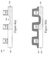
- FIGS. 4( a ) through 4 ( d ) are a series of cross sectional views illustrating a method of STI recess repair prior to silicide processing, in accordance with an alternative embodiment of the invention.
- the starting structure (i.e., semiconductor device 200 ) of FIG. 4( a ) is similar to that of FIG. 2( a ).
- a nitride spacer layer 402 is formed over the active region 202 and STI region 204 , including the recess 208 .
- the nitride spacer layer 402 has a thickness that is suitable both for gate spacer formation on the active region 202 , as wall as to fill the recess 208 .
- the STI region 204 is masked with a protective layer 404 , such as a photoresist or hardmask layer so as to expose only the portions of the nitride layer 402 over the active area 202 , as shown in FIG. 4( c ). Then, as shown in FIG. 4( d ), the RIE forms nitride spacers 406 adjacent the gate structures of the active region 202 , while the nitride layer 210 remains over the STI region as originally deposited. Instead of serving as a spacer layer in this region, the nitride layer 402 may instead be used as part of the nitride cap layer prior to ILD formation.
- a protective layer 404 such as a photoresist or hardmask layer
Landscapes
- Insulated Gate Type Field-Effect Transistor (AREA)
- Element Separation (AREA)
- Metal-Oxide And Bipolar Metal-Oxide Semiconductor Integrated Circuits (AREA)
Abstract
Description
Claims (13)
Priority Applications (1)
| Application Number | Priority Date | Filing Date | Title |
|---|---|---|---|
| US12/914,095 US8765491B2 (en) | 2010-10-28 | 2010-10-28 | Shallow trench isolation recess repair using spacer formation process |
Applications Claiming Priority (1)
| Application Number | Priority Date | Filing Date | Title |
|---|---|---|---|
| US12/914,095 US8765491B2 (en) | 2010-10-28 | 2010-10-28 | Shallow trench isolation recess repair using spacer formation process |
Publications (2)
| Publication Number | Publication Date |
|---|---|
| US20120104500A1 US20120104500A1 (en) | 2012-05-03 |
| US8765491B2 true US8765491B2 (en) | 2014-07-01 |
Family
ID=45995724
Family Applications (1)
| Application Number | Title | Priority Date | Filing Date |
|---|---|---|---|
| US12/914,095 Expired - Fee Related US8765491B2 (en) | 2010-10-28 | 2010-10-28 | Shallow trench isolation recess repair using spacer formation process |
Country Status (1)
| Country | Link |
|---|---|
| US (1) | US8765491B2 (en) |
Cited By (4)
| Publication number | Priority date | Publication date | Assignee | Title |
|---|---|---|---|---|
| US10263013B2 (en) | 2017-02-24 | 2019-04-16 | Globalfoundries Inc. | Method of forming an integrated circuit (IC) with hallow trench isolation (STI) regions and the resulting IC structure |
| US10546775B1 (en) | 2018-08-01 | 2020-01-28 | Globalfoundries Inc. | Field-effect transistors with improved dielectric gap fill |
| US10714376B2 (en) | 2018-06-25 | 2020-07-14 | Globalfoundries Inc. | Method of forming semiconductor material in trenches having different widths, and related structures |
| US11171036B2 (en) | 2019-10-09 | 2021-11-09 | Globalfoundries U.S. Inc. | Preventing dielectric void over trench isolation region |
Families Citing this family (6)
| Publication number | Priority date | Publication date | Assignee | Title |
|---|---|---|---|---|
| US20140159157A1 (en) * | 2012-12-07 | 2014-06-12 | Altera Corporation | Antenna diode circuitry and method of manufacture |
| US9257438B2 (en) * | 2014-01-17 | 2016-02-09 | Taiwan Semiconductor Manufacturing Co., Ltd. | Semiconductor device structure and method of manufacturing the same |
| CN105742248A (en) * | 2014-12-09 | 2016-07-06 | 中芯国际集成电路制造(上海)有限公司 | Method for forming semiconductor structure |
| FR3100084B1 (en) * | 2019-08-23 | 2021-10-01 | Commissariat Energie Atomique | microelectronic component manufacturing process |
| US11145727B2 (en) | 2019-10-29 | 2021-10-12 | Nanya Technology Corporation | Semiconductor structure and method of forming the same |
| CN115799161B (en) * | 2023-01-09 | 2023-05-09 | 广州粤芯半导体技术有限公司 | Semiconductor structure and preparation method thereof |
Citations (17)
| Publication number | Priority date | Publication date | Assignee | Title |
|---|---|---|---|---|
| US6146970A (en) | 1998-05-26 | 2000-11-14 | Motorola Inc. | Capped shallow trench isolation and method of formation |
| US6165871A (en) | 1999-07-16 | 2000-12-26 | Chartered Semiconductor Manufacturing Ltd. | Method of making low-leakage architecture for sub-0.18 μm salicided CMOS device |
| US6251747B1 (en) | 1999-11-02 | 2001-06-26 | Philips Semiconductors, Inc. | Use of an insulating spacer to prevent threshold voltage roll-off in narrow devices |
| US20020158286A1 (en) * | 2000-02-08 | 2002-10-31 | Chediak Juan A. | Symmetric device with contacts self aligned to gate |
| US6657244B1 (en) * | 2002-06-28 | 2003-12-02 | International Business Machines Corporation | Structure and method to reduce silicon substrate consumption and improve gate sheet resistance during silicide formation |
| US6802944B2 (en) * | 2002-10-23 | 2004-10-12 | Applied Materials, Inc. | High density plasma CVD process for gapfill into high aspect ratio features |
| US7087531B1 (en) * | 2005-01-17 | 2006-08-08 | International Business Machines Corporation | Shallow trench isolation formation |
| US7087483B2 (en) | 2003-11-25 | 2006-08-08 | Taiwan Semiconductor Manufacturing Co., Ltd. | Single transistor RAM cell and method of manufacture |
| US7179711B2 (en) | 1997-03-28 | 2007-02-20 | Renesas Technology Corp. | Non-volatile semiconductor memory and method of making same, and semiconductor device and method of making device |
| US7223698B1 (en) | 2005-02-10 | 2007-05-29 | Advanced Micro Devices, Inc. | Method of forming a semiconductor arrangement with reduced field-to active step height |
| US7335545B2 (en) | 2002-06-07 | 2008-02-26 | Amberwave Systems Corporation | Control of strain in device layers by prevention of relaxation |
| US20080237733A1 (en) | 2007-03-27 | 2008-10-02 | International Business Machines Corporation | Structure and method to enhance channel stress by using optimized sti stress and nitride capping layer stress |
| US20090023258A1 (en) | 2007-07-17 | 2009-01-22 | Chia-Wen Liang | Method of manufacturing complementary metal oxide semiconductor transistors |
| US20090032900A1 (en) * | 2007-08-03 | 2009-02-05 | United Microelectronics Corp. | Method of protecting shallow trench isolation structure and composite structure resulting from the same |
| US7488660B2 (en) | 2006-02-21 | 2009-02-10 | International Business Machines Corporation | Extended raised source/drain structure for enhanced contact area and method for forming extended raised source/drain structure |
| US20090184341A1 (en) | 2008-01-17 | 2009-07-23 | Chartered Semiconductor Manufacturing, Ltd. | Elimination of STI recess and facet growth in embedded silicon-germanium (eSiGe) module |
| US20110115000A1 (en) * | 2009-11-19 | 2011-05-19 | Qualcomm Incorporated | Semiconductor Device having Strain Material |
-
2010
- 2010-10-28 US US12/914,095 patent/US8765491B2/en not_active Expired - Fee Related
Patent Citations (17)
| Publication number | Priority date | Publication date | Assignee | Title |
|---|---|---|---|---|
| US7179711B2 (en) | 1997-03-28 | 2007-02-20 | Renesas Technology Corp. | Non-volatile semiconductor memory and method of making same, and semiconductor device and method of making device |
| US6146970A (en) | 1998-05-26 | 2000-11-14 | Motorola Inc. | Capped shallow trench isolation and method of formation |
| US6165871A (en) | 1999-07-16 | 2000-12-26 | Chartered Semiconductor Manufacturing Ltd. | Method of making low-leakage architecture for sub-0.18 μm salicided CMOS device |
| US6251747B1 (en) | 1999-11-02 | 2001-06-26 | Philips Semiconductors, Inc. | Use of an insulating spacer to prevent threshold voltage roll-off in narrow devices |
| US20020158286A1 (en) * | 2000-02-08 | 2002-10-31 | Chediak Juan A. | Symmetric device with contacts self aligned to gate |
| US7335545B2 (en) | 2002-06-07 | 2008-02-26 | Amberwave Systems Corporation | Control of strain in device layers by prevention of relaxation |
| US6657244B1 (en) * | 2002-06-28 | 2003-12-02 | International Business Machines Corporation | Structure and method to reduce silicon substrate consumption and improve gate sheet resistance during silicide formation |
| US6802944B2 (en) * | 2002-10-23 | 2004-10-12 | Applied Materials, Inc. | High density plasma CVD process for gapfill into high aspect ratio features |
| US7087483B2 (en) | 2003-11-25 | 2006-08-08 | Taiwan Semiconductor Manufacturing Co., Ltd. | Single transistor RAM cell and method of manufacture |
| US7087531B1 (en) * | 2005-01-17 | 2006-08-08 | International Business Machines Corporation | Shallow trench isolation formation |
| US7223698B1 (en) | 2005-02-10 | 2007-05-29 | Advanced Micro Devices, Inc. | Method of forming a semiconductor arrangement with reduced field-to active step height |
| US7488660B2 (en) | 2006-02-21 | 2009-02-10 | International Business Machines Corporation | Extended raised source/drain structure for enhanced contact area and method for forming extended raised source/drain structure |
| US20080237733A1 (en) | 2007-03-27 | 2008-10-02 | International Business Machines Corporation | Structure and method to enhance channel stress by using optimized sti stress and nitride capping layer stress |
| US20090023258A1 (en) | 2007-07-17 | 2009-01-22 | Chia-Wen Liang | Method of manufacturing complementary metal oxide semiconductor transistors |
| US20090032900A1 (en) * | 2007-08-03 | 2009-02-05 | United Microelectronics Corp. | Method of protecting shallow trench isolation structure and composite structure resulting from the same |
| US20090184341A1 (en) | 2008-01-17 | 2009-07-23 | Chartered Semiconductor Manufacturing, Ltd. | Elimination of STI recess and facet growth in embedded silicon-germanium (eSiGe) module |
| US20110115000A1 (en) * | 2009-11-19 | 2011-05-19 | Qualcomm Incorporated | Semiconductor Device having Strain Material |
Non-Patent Citations (1)
| Title |
|---|
| IBM, "Technical Disclosure: A Simple Method to Reduce STI Recess for Stress Nitride Fill at Sub-32nm Technology Nodes," published by IBM on Apr. 22, 2009, in IP.COM, IPCOM000182028D. |
Cited By (5)
| Publication number | Priority date | Publication date | Assignee | Title |
|---|---|---|---|---|
| US10263013B2 (en) | 2017-02-24 | 2019-04-16 | Globalfoundries Inc. | Method of forming an integrated circuit (IC) with hallow trench isolation (STI) regions and the resulting IC structure |
| US10903207B2 (en) | 2017-02-24 | 2021-01-26 | Globalfoundries Inc. | Method of forming an integrated circuit (IC) with shallow trench isolation (STI) regions and the resulting IC structure |
| US10714376B2 (en) | 2018-06-25 | 2020-07-14 | Globalfoundries Inc. | Method of forming semiconductor material in trenches having different widths, and related structures |
| US10546775B1 (en) | 2018-08-01 | 2020-01-28 | Globalfoundries Inc. | Field-effect transistors with improved dielectric gap fill |
| US11171036B2 (en) | 2019-10-09 | 2021-11-09 | Globalfoundries U.S. Inc. | Preventing dielectric void over trench isolation region |
Also Published As
| Publication number | Publication date |
|---|---|
| US20120104500A1 (en) | 2012-05-03 |
Similar Documents
| Publication | Publication Date | Title |
|---|---|---|
| US8765491B2 (en) | Shallow trench isolation recess repair using spacer formation process | |
| US20210296257A1 (en) | Fabrication method of semiconductor structure | |
| US7442607B2 (en) | Method of manufacturing transistor having recessed channel | |
| US20130307079A1 (en) | Etch resistant barrier for replacement gate integration | |
| US7838356B2 (en) | Gate dielectric first replacement gate processes and integrated circuits therefrom | |
| US10319679B2 (en) | Semiconductor device | |
| US9318445B2 (en) | Semiconductor device and manufacturing method thereof for protecting metal-gate from oxidation | |
| US10008409B2 (en) | Method for fabricating a semiconductor device | |
| CN102543838B (en) | Manufacturing method of semiconductor device | |
| US11114542B2 (en) | Semiconductor device with reduced gate height budget | |
| CN110246804B (en) | Contact structure | |
| US7820537B1 (en) | Method for fabricating semiconductor device | |
| US9006809B2 (en) | Multi-landing contact etching | |
| US7323377B1 (en) | Increasing self-aligned contact areas in integrated circuits using a disposable spacer | |
| US7745298B2 (en) | Method of forming a via | |
| US6773975B1 (en) | Formation of a shallow trench isolation structure in integrated circuits | |
| KR20110078105A (en) | How to Form Butting Contact of Semiconductor Device | |
| KR100945870B1 (en) | Method for forming multilayer wiring of semiconductor device | |
| JP2007081347A (en) | Method for manufacturing semiconductor device | |
| KR100945867B1 (en) | Method for forming multilayer wiring of semiconductor device | |
| US9362123B2 (en) | Structure and method for integrated devices on different substartes with interfacial engineering | |
| US20180342394A1 (en) | Manufacturing method of semiconductor structure | |
| KR20080097836A (en) | Manufacturing method of semiconductor device | |
| KR20060117804A (en) | Method of forming recess gate of semiconductor device | |
| KR20070016371A (en) | Transistor Formation Method With Recess Channel |
Legal Events
| Date | Code | Title | Description |
|---|---|---|---|
| AS | Assignment |
Owner name: INTERNATIONAL BUSINESS MACHINES CORPORATION, NEW Y Free format text: ASSIGNMENT OF ASSIGNORS INTEREST;ASSIGNORS:CAI, MING;LI, XI;TAMWEBER, FRANK D., JR.;SIGNING DATES FROM 20101026 TO 20101027;REEL/FRAME:025210/0503 |
|
| AS | Assignment |
Owner name: GLOBALFOUNDRIES U.S. 2 LLC, NEW YORK Free format text: ASSIGNMENT OF ASSIGNORS INTEREST;ASSIGNOR:INTERNATIONAL BUSINESS MACHINES CORPORATION;REEL/FRAME:036550/0001 Effective date: 20150629 |
|
| AS | Assignment |
Owner name: GLOBALFOUNDRIES INC., CAYMAN ISLANDS Free format text: ASSIGNMENT OF ASSIGNORS INTEREST;ASSIGNORS:GLOBALFOUNDRIES U.S. 2 LLC;GLOBALFOUNDRIES U.S. INC.;REEL/FRAME:036779/0001 Effective date: 20150910 |
|
| FEPP | Fee payment procedure |
Free format text: MAINTENANCE FEE REMINDER MAILED (ORIGINAL EVENT CODE: REM.) |
|
| LAPS | Lapse for failure to pay maintenance fees |
Free format text: PATENT EXPIRED FOR FAILURE TO PAY MAINTENANCE FEES (ORIGINAL EVENT CODE: EXP.) |
|
| STCH | Information on status: patent discontinuation |
Free format text: PATENT EXPIRED DUE TO NONPAYMENT OF MAINTENANCE FEES UNDER 37 CFR 1.362 |
|
| AS | Assignment |
Owner name: GLOBALFOUNDRIES U.S. INC., NEW YORK Free format text: RELEASE BY SECURED PARTY;ASSIGNOR:WILMINGTON TRUST, NATIONAL ASSOCIATION;REEL/FRAME:056987/0001 Effective date: 20201117 |