US8721394B2 - Polishing pad and polishing method - Google Patents
Polishing pad and polishing method Download PDFInfo
- Publication number
- US8721394B2 US8721394B2 US11/960,451 US96045107A US8721394B2 US 8721394 B2 US8721394 B2 US 8721394B2 US 96045107 A US96045107 A US 96045107A US 8721394 B2 US8721394 B2 US 8721394B2
- Authority
- US
- United States
- Prior art keywords
- polishing
- grooves
- polishing pad
- tracking zone
- substrate
- Prior art date
- Legal status (The legal status is an assumption and is not a legal conclusion. Google has not performed a legal analysis and makes no representation as to the accuracy of the status listed.)
- Active, expires
Links
- 238000005498 polishing Methods 0.000 title claims abstract description 322
- 238000000034 method Methods 0.000 title claims abstract description 31
- 239000000758 substrate Substances 0.000 claims abstract description 86
- 239000002002 slurry Substances 0.000 claims description 10
- 239000011295 pitch Substances 0.000 claims description 5
- 230000001788 irregular Effects 0.000 claims description 4
- 239000000463 material Substances 0.000 description 5
- 238000007517 polishing process Methods 0.000 description 5
- 229920000642 polymer Polymers 0.000 description 5
- 238000012986 modification Methods 0.000 description 3
- 230000004048 modification Effects 0.000 description 3
- 239000003082 abrasive agent Substances 0.000 description 2
- 239000000126 substance Substances 0.000 description 2
- 235000012431 wafers Nutrition 0.000 description 2
- 239000005062 Polybutadiene Substances 0.000 description 1
- 239000004721 Polyphenylene oxide Substances 0.000 description 1
- 239000000654 additive Substances 0.000 description 1
- 239000006227 byproduct Substances 0.000 description 1
- 239000000969 carrier Substances 0.000 description 1
- 239000003054 catalyst Substances 0.000 description 1
- 239000000919 ceramic Substances 0.000 description 1
- 238000006243 chemical reaction Methods 0.000 description 1
- 239000003638 chemical reducing agent Substances 0.000 description 1
- 239000003795 chemical substances by application Substances 0.000 description 1
- 239000004020 conductor Substances 0.000 description 1
- 239000011521 glass Substances 0.000 description 1
- 239000003112 inhibitor Substances 0.000 description 1
- 239000007800 oxidant agent Substances 0.000 description 1
- 229920000058 polyacrylate Polymers 0.000 description 1
- 229920002857 polybutadiene Polymers 0.000 description 1
- 229920000515 polycarbonate Polymers 0.000 description 1
- 239000004417 polycarbonate Substances 0.000 description 1
- 229920000728 polyester Polymers 0.000 description 1
- 229920000570 polyether Polymers 0.000 description 1
- 229920000307 polymer substrate Polymers 0.000 description 1
- 229920002635 polyurethane Polymers 0.000 description 1
- 239000004814 polyurethane Substances 0.000 description 1
- 230000002250 progressing effect Effects 0.000 description 1
- 229920005989 resin Polymers 0.000 description 1
- 239000011347 resin Substances 0.000 description 1
- 239000004065 semiconductor Substances 0.000 description 1
- 239000007787 solid Substances 0.000 description 1
- 239000000243 solution Substances 0.000 description 1
- 229920005992 thermoplastic resin Polymers 0.000 description 1
- 229920001187 thermosetting polymer Polymers 0.000 description 1
Images


Classifications
-
- B—PERFORMING OPERATIONS; TRANSPORTING
- B24—GRINDING; POLISHING
- B24B—MACHINES, DEVICES, OR PROCESSES FOR GRINDING OR POLISHING; DRESSING OR CONDITIONING OF ABRADING SURFACES; FEEDING OF GRINDING, POLISHING, OR LAPPING AGENTS
- B24B37/00—Lapping machines or devices; Accessories
- B24B37/11—Lapping tools
- B24B37/20—Lapping pads for working plane surfaces
- B24B37/26—Lapping pads for working plane surfaces characterised by the shape of the lapping pad surface, e.g. grooved
Definitions
- the present invention relates to a polishing pad and a polishing method. More particularly, the present invention relates to a polishing pad and a polishing method capable of achieving a better polishing uniformity of a substrate surface.
- substrates e.g., semiconductor wafers, III-V wafers, storage device carriers, ceramic substrates, polymer substrates, and glass substrates
- substrates e.g., semiconductor wafers, III-V wafers, storage device carriers, ceramic substrates, polymer substrates, and glass substrates
- a polishing process is often adopted in the industry.
- a pressure is applied on a substrate, so as to press the substrate on a polishing pad, and a relative motion between the substrate and the polishing pad is provided. Through the friction generated by the relative motion, a portion of the substrate surface is removed, such that the surface is planarized gradually.
- FIG. 1 is a schematic top view of a conventional polishing pad.
- the polishing pad 100 includes a polishing layer 110 and a plurality of circumferential grooves 120 .
- the polishing layer 110 is in contact with a surface of a substrate 130 .
- the plurality of circumferential grooves 120 are arranged in concentric circles, and a center of the circumferential grooves 120 coincides with a rotational axis C 0 of the polishing pad 100 .
- the circumferential grooves 120 are used to accommodate or remove the polishing residues or byproducts, and enable the substrate 130 to be easily detached away from the polishing pad 100 when the polishing is completed.
- the substrate 130 on the surface of the polishing pad 100 rotates as well, expecting that all positions of the surface of the substrate 130 are able to contact with the circumferential grooves 120 .
- the circumferential grooves 120 of the conventional polishing pad 100 are concentric circular grooves, and the substrate 130 rotates around its central axis, when a specific point of the substrate 130 moves to a region parallel to tangential direction of the grooves 120 , the specific point will be constantly on the groove portion or the non-groove portion. For example, when the specific point is on the groove portion, points near the specific point will be constantly on the non-groove portion, which results in an unfavorable polishing uniformity.
- the central portion of the substrate 130 is almost constantly in contact with a specific portion (e.g., the groove portion or the non-groove portion) on the polishing pad 100 . Therefore, the polishing rate at the central portion of the substrate 130 will be lower or higher than the polishing rate of other near portions, depending on whether the central portion is constantly positioned on the groove portion or the non-groove portion.
- the problem that the polishing rate of the substrate 130 is not uniform may eventually suffer the reliability of the devices.
- the present invention is directed to a polishing pad, which enables polishing rates of a substrate surface to have a better uniformity.
- the present invention is also directed to a polishing method, which helps to obtain a substrate with a planar surface.
- the present invention provides a polishing pad suitable for polishing a substrate.
- the polishing pad includes a polishing layer and at least two grooves.
- the polishing layer has an even tracking zone disposed around a rotational axis.
- the grooves are disposed in the even tracking zone, and satisfy the following relation: D (i)max ⁇ D (i+n)min
- D (i)max is the largest distance from the rotational axis to the (i) th groove
- D (i+n)min is the smallest distance from the rotational axis to the (i+n) th groove
- i is an ordinal number of a groove counting from the groove closest to the rotational axis to an outer periphery of the even tracking zone
- n is an integer.
- the present invention further provides a polishing pad suitable for polishing a substrate.
- the polishing pad includes a polishing layer and at least two grooves.
- the polishing layer has an even tracking zone.
- the grooves are disposed in the even tracking zone.
- Each of the grooves forms one polishing track, and the polishing tracks are adjoining one another.
- the present invention still provides a polishing pad suitable for polishing a substrate.
- the polishing pad includes a polishing layer.
- the polishing layer has an even tracking zone.
- the even tracking zone is divided into at least two polishing tracks, and the polishing tracks are adjoining one another.
- at least one groove is disposed in each of the polishing tracks, and the at least one groove has a uniformly distributed trajectory in each of the polishing tracks.
- the present invention also provides a polishing method for polishing a substrate. Firstly, a polishing pad is provided. Then, a pressure is applied on the substrate to press the substrate on the polishing pad. Next, a relative motion is provided between the substrate and the polishing pad.
- the polishing pad includes a polishing layer and at least two grooves.
- the polishing layer has an even tracking zone disposed around a rotational axis. The grooves are disposed in the even tracking zone, and satisfy the following relation: D (i)max ⁇ D (i+n)min
- D (i)max is the largest distance from the rotational axis to the (i) th groove
- D (i+n)min is the smallest distance from the rotational axis to the (i+n) th groove
- i is an ordinal number of a groove counting from the groove closest to the rotational axis to an outer periphery of the even tracking zone
- n is an integer.
- the present invention further provides a polishing method for polishing a substrate. Firstly, a polishing pad is provided. Then, a pressure is applied on the substrate to press the substrate on the polishing pad. Next, a relative motion is provided between the substrate and the polishing pad.
- the polishing pad includes a polishing layer and at least two grooves.
- the polishing layer has an even tracking zone. The grooves are disposed in the even tracking zone. Each of the grooves forms one polishing track, and the polishing tracks are adjoining one another.
- the present invention still provides a polishing method for polishing a substrate. Firstly, a polishing pad is provided. Then, a pressure is applied on the substrate to press the substrate on the polishing pad. Next, a relative motion is provided between the substrate and the polishing pad.
- the polishing pad includes a polishing layer.
- the polishing layer has an even tracking zone. The even tracking zone is divided into at least two polishing tracks, and the polishing tracks are adjoining one another. At least one groove is disposed in each of the polishing tracks, and the at least one groove has a uniformly distributed trajectory in each of the polishing tracks.
- the polishing pad and the polishing method of the present invention adopt the polishing pad with a specific groove design, so a polishing process using the polishing pad may achieve a better polishing uniformity of a polished substrate surface.
- FIG. 1 is a schematic top view of a conventional polishing pad.
- FIG. 2A is a schematic top view of a polishing pad according to an embodiment of the present invention.
- FIG. 2B is a schematic top view of a polishing pad according to another embodiment of the present invention.
- FIGS. 3A to 3F are schematic top views of patterns of grooves according to several embodiments of the present invention.
- FIG. 4 is a schematic top view of a groove arrangement according to an embodiment of the present invention.
- FIGS. 5A and 5B are schematic top views of groove arrangements according to other embodiments of the present invention.
- FIG. 6 is a schematic top view of grooves according to still another embodiment of the present invention.
- the polishing method of the present invention is suitable for polishing a substrate. Firstly, a polishing pad is provided.
- the polishing pad for example, has a specific groove design, in which each groove forms a corresponding polishing track, and the polishing tracks form an even tracking zone. Then, a pressure is applied on the substrate to press the substrate on the polishing pad. Next, a relative motion is provided between the substrate and the polishing pad, so as to remove a portion of a substrate surface to achieve planarization.
- the polishing method of the present invention may achieve a better polishing uniformity of the substrate surface.
- slurry or solution may be optionally supplied during polishing. Thus, the polishing method becomes a chemical mechanical polishing (CMP) process.
- CMP chemical mechanical polishing
- FIG. 2A is a schematic top view of a polishing pad according to an embodiment of the present invention.
- the polishing pad 200 is suitable for polishing a surface of a substrate 240 during polishing.
- the polishing pad 200 for example, is made of a polymer base material, and the polymer base material may be polyester, polyether, polyurethane, polycarbonate, polyacrylate, polybutadiene, or other polymer base materials formed by appropriate thermosetting resins or thermoplastic resins.
- the polishing pad 200 may further include conductive materials, abrasives, or soluble additives in the polymer base material.
- the polishing pad 200 includes a polishing layer 210 and at least two grooves 220 .
- the polishing layer 210 has an even tracking zone 212 .
- the even tracking zone 212 is an area formed by uniformly distributed trajectories along which the grooves 220 relatively pass when the polishing pad 200 rotates.
- the even tracking zone 212 for example, is disposed corresponding to a central portion of the substrate 240 .
- the even tracking zone 212 for example, is disposed around a rotational axis C 1 .
- the rotational axis C 1 extends in a direction perpendicular to the polishing layer 210 . In detail, as shown in FIG.
- the even tracking zone 212 is substantially disposed in a middle region between the innermost portion and the outermost portion of the polishing pad 200 , i.e., in an area between a border 212 a and a border 212 b .
- the even tracking zone 212 for example, is annular, and has a geometrical center coinciding with the rotational axis C 1 .
- the central portion of the substrate 240 will alternately pass the groove portion and the nor-groove portion instead of constantly contacting the groove portion or the non-groove portion on the polishing pad 200 . Therefore, the polishing rates of the central portion and other near portions of the substrate 240 are more consistent.
- the even tracking zone 212 has a width of at least 35 mm, for example, between 40 mm and a maximum dimension of the substrate 240 .
- other grooves may also be disposed in the portion outside the even tracking zone 212 .
- the even tracking zone 212 may also be optionally disposed in almost entire surface of the polishing pad 200 .
- the width of the even tracking zone 212 may be up to 95% of a radius of the polishing pad 200 .
- the grooves 220 are disposed in the even tracking zone 212 .
- the grooves 220 for example, are enclosed grooves, and are not interconnected.
- each of the grooves 220 for example, forms one polishing track 230 , and the polishing tracks 230 collectively construct the even tracking zone 212 .
- a better polishing uniformity of the surface of the substrate 240 is achieved with the even tracking zone 212 .
- the grooves 220 are elliptical grooves, and the grooves 220 , for example, have a common geometrical center. That is to say, the geometrical center of the elliptical grooves coincides with the rotational axis C 1 .
- a major axis of each elliptical groove for example, is set on the same axis, i.e., the grooves 220 are coaxial.
- the radial pitches between the grooves 220 are the same.
- each of the grooves 220 will generate one polishing track 230 .
- the polishing tracks 230 are concentric with the rotational axis C 1 . Furthermore, the polishing tracks 230 are adjoining one another. For example, the polishing tracks 230 have the same width W. In other words, the even tracking zone 212 , for example, is divided into at least two polishing tracks 230 adjoining one another, and at least one groove 220 is disposed in each of the polishing tracks 230 , such that the at least one groove 220 may form a uniformly distributed trajectory in each of the polishing tracks 230 .
- the polishing pad 200 may provide a uniform polishing rate on every portion of the surface of the substrate 240 .
- grooves 220 satisfy the following relation: D (i)max ⁇ D (i+n)max
- D (i)max is the largest distance from the rotational axis C 1 to the (i) th groove 220
- D (i+n)min is the smallest distance from the rotational axis C 1 to the (i+n) th groove 220
- i is an ordinal number of a groove 220 counting from the groove 220 closest to the rotational axis C 1 to an outer periphery of the even tracking zone 212
- n is an integer between 1 and 5, for example.
- the largest distance D (i)max from the rotational axis C 1 to the (i) th groove 220 is approximately equal to or substantially equal to the smallest distance from the rotational axis C 1 to the (i+n) th groove 220 .
- the grooves 220 satisfies the relation: D (i)max ⁇ D (i+1)min .
- the largest distance D (1)max from the rotational axis C 1 to the first groove 220 is the major axis of the first groove 220
- the smallest distance D (2)min from the rotational axis C 1 to the second groove 220 is the minor axis of the second groove 220 , wherein D (1)max ⁇ D (2)min .
- the polishing tracks 230 formed by the grooves 220 are adjoining one another to construct the even tracking zone 212 , i.e., no non-track region is formed between the polishing tracks 230 .
- FIG. 2A is taken as an example, but the present invention is not limited to this.
- FIG. 2B is a schematic top view of a polishing pad according to another embodiment of the present invention.
- D (i)max ⁇ D (i+2)min .
- the largest distance D (1)max from the rotational axis C 1 to the first groove 220 a is the major axis of the first groove 220 a
- the smallest distance D (3)min from the rotational axis C 1 to the third groove 220 is the minor axis of the third groove 220 , wherein D (1)max ⁇ D (3)min .
- the polishing tracks 230 a for example, have a width of W a .
- the grooves 220 a in FIG. 2B are elliptical grooves in which the major axis and the minor axis differ more.
- the polishing tracks 230 a generated corresponding to the grooves 220 a may have a larger width W a , and the polishing tracks 230 a may be partially overlapped one another. Areas of the same overlapping ratio (areas between the border 212 a and the border 212 b ) of the polishing tracks 230 a construct the even tracking area 212 . A better polishing uniformity of the surface of the substrate 240 a is achieved with the even tracking zone 212 .
- the polishing pads 200 , 200 a with elliptical grooves are exemplified for illustration, but the present invention is not limited to this. In other embodiments, the grooves may also be in other shapes. Hereinafter, the grooves of different patterns will be illustrated.
- FIGS. 3A to 3E are schematic top views of groove patterns according to several embodiments of the present invention.
- FIGS. 3A to 3F the same components in FIG. 2 are indicated by the same reference numerals, and will not be described again.
- the grooves 220 c are polygonal grooves.
- the grooves 220 c are quadrangular grooves with four round corners 300 .
- the grooves 220 c thus will form the polishing tracks 230 c with a width W c and adjoining one another.
- the polishing tracks 230 c collectively construct the even tracking zone. A better polishing uniformity of the substrate surface is achieved with the even tracking zone.
- the grooves 220 d may also be corrugated grooves with a plurality of round corners as shown in FIG. 3B .
- the corrugated grooves thus form the polishing tracks 230 d with a width W d and adjoining one another.
- the polishing tracks 230 d collectively construct the even tracking zone. A better polishing uniformity of the substrate surface is achieved with the even tracking zone.
- the grooves 220 e may be annular grooves having at least one protrusion and/or at least one recession.
- the grooves 220 e are a plurality of annular grooves having a plurality of protrusions 310 , and the protrusions 310 protrude from projected peripheries of the annular grooves.
- the annular grooves having the protrusions 310 will from polishing tricks 230 e with a width W c and adjoining one another.
- the polishing tracks 230 e collectively construct the even tracking zone. A better polishing uniformity of the substrate surface is achieved with the even tracking zone.
- the grooves 220 f may also be circumferential grooves with a geometrical center, for example, deviated from the rotational axis C 1 .
- the grooves 220 f are circular grooves with a center C 2 deviated from the rotational axis C 1 , i.e., the center C 2 does not coincide with the rotational axis C 1 .
- the grooves 220 f will form polishing tracks 230 f with a width W f and adjoining one another.
- the polishing tracks 230 f collectively construct the even tracking zone. A better polishing uniformity of the substrate surface is achieved with the even tracking zone.
- the grooves 220 b in each of the polishing tracks 230 b may include two intersecting elliptical grooves with the same length of major axis and the same length of minor axis.
- the major axes of the two elliptical grooves may be perpendicular to each other.
- the grooves 220 b for example, are dual-elliptical grooves formed by two elliptical grooves.
- the grooves 220 b will form polishing tracks 230 b with a width W b and adjoining one another.
- the polishing tracks 230 b collectively construct the even tracking zone. A better polishing uniformity of the substrate surface is achieved with the even tracking zone.
- the largest distance from the rotational axis C 1 to the first groove 220 c , 220 d , 220 e , 220 f , and 220 b is equal to the smallest distance from the rotational axis C 1 to the second groove 220 c , 220 d , 220 e , 220 f , and 220 b .
- the grooves 220 c , 220 d , 220 e , 220 f , and 220 b all satisfy the relation D (1)max ⁇ D (2)min . Therefore, the grooves 220 c , 220 d , 220 e , 220 f , and 220 b may construct the even tracking zone, so as to provide a better polishing uniformity of the substrate surface.
- the grooves of the polishing pad may be in other irregular shapes, or any combination of the grooves 220 c , 220 d , 220 e , 220 f , and 220 b in different patterns as shown in FIGS. 3A to 3E , as long as the grooves on the polishing pad satisfy the relation D (i)max ⁇ D (i+n)min .
- Persons skilled in the art can make proper adjustment according to actual requirements.
- the present invention may also be implemented in other forms.
- the grooves are arranged corresponding to the same axis, the pitches between every two adjoining grooves are the same in radial direction, and the adjoining polishing tracks have the same width.
- the present invention is not limited to this. In other embodiments, the pitches of every two adjoining grooves may be different in the radial direction, which will be illustrated in detail below.
- FIG. 4 is a schematic top view of a groove arrangement according to an embodiment of the present invention.
- different grooves 221 are arranged corresponding to different axes, i.e., the grooves 221 are arranged non-coaxially.
- the grooves 221 will form polishing tracks 231 , and the polishing tracks 231 , for example, have the same width W 1 .
- FIGS. 5A and 5B are schematic top views of a groove arrangement according to other embodiments of the present invention.
- the grooves 222 , 223 , and 224 are the first, second, and third grooves sequentially counting from the one closest to the rotational axis C 1 .
- the grooves 222 , 223 , and 224 will form polishing tracks 232 , 233 , and 234 with widths W 2 , W 3 , and W 4 respectively.
- the grooves 222 , 223 , and 224 are arranged corresponding to the same axis.
- the width W 2 of the polishing track 232 , the width W 3 of the polishing track 233 , and the width W 4 of the polishing track 234 are not completely the same.
- the grooves 225 , 226 , and 227 are the first, second, and third grooves counting from the one closest to the rotational axis C 1 respectively.
- the grooves 225 , 226 , and 227 will form polishing tracks 235 , 236 , and 237 with widths W 5 , W 6 , and W 7 respectively.
- the grooves 225 , 226 , and 227 are arranged non-coaxially.
- the widths W 5 , W 6 , and W 7 of the polishing tracks 231 , 232 , and 233 are not completely the same.
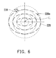
- FIG. 6 is a schematic top view of the grooves according to another embodiment of the present invention.
- the grooves 228 on the polishing pad may also include a plurality of discontinuous sub-grooves 228 a .
- the grooves 228 are in a discontinuous enclosure shape.
- the sub-grooves 228 a constructing each of the discontinuous enclosure shape of the grooves 228 will form a polishing track 238 with a width W 8 .
- the polishing tracks 238 collectively construct the even tracking zone. A better polishing uniformity of the substrate surface is achieved with the even tracking zone.
- the grooves of the above embodiments all satisfy the relation D (i)max ⁇ D (i+n)min . Therefore, during polishing, the polishing tracks formed by the grooves will collectively construct the even tracking zone, which helps to achieve a uniform polishing rate on different portions of the substrate surface.
- FIGS. 4 , 5 A, 5 B, and 6 oily three grooves are shown and the elliptical grooves are taken as an example for simplifying the drawings, such that persons skilled in the art can implement the present invention accordingly.
- the present invention is not limited to this. Persons skilled in the art can appreciate the applications and variations of the present invention, which will not be described herein.
- round polishing pads are taken as an example for illustrating the present invention.
- the polishing pads may also in other shapes, e.g., rings, squares, or strips, depending on the requirements of polishing equipment.
- the grooves in the polishing tracks may also be in other shapes, as long as the grooves may construct the even tracking zone and the polishing rate is uniform, which are not particularly limited in the present invention, and persons of ordinary skill in the art can make modifications according to actual requirements.
- the slurries or solutions with different properties may be supplied in different polishing tracks.
- the properties include viscosity of the slurry or solution, concentration of chemicals (e.g., oxidizing agents, reducing agents, complex agents, inhibitors, and catalysts) in the slurry or solution, or solid content or abrasive content in the slurry.
- the grooves in different polishing tracks are not interconnected, so the polishing capability differs in different polishing tracks, thereby adjusting the polishing rate distribution profile.
- the slurry containing more abrasives may be optionally supplied into the polishing tracks corresponding to the near edge region of the substrate to increase the polishing rate of the near edge region of the substrate.
- the groove design of the polishing pad of the present invention may construct the even tracking zone, and with the even tracking zone, a better polishing uniformity of the substrate surface may be achieved.
- the polishing method of the present invention adopts the polishing pad having the even tracking zone, thereby helping to provide a more uniform and planar substrate surface.
Landscapes
- Engineering & Computer Science (AREA)
- Mechanical Engineering (AREA)
- Mechanical Treatment Of Semiconductor (AREA)
- Finish Polishing, Edge Sharpening, And Grinding By Specific Grinding Devices (AREA)
Abstract
Description
D(i)max≅D(i+n)min
D(i)max≅D(i+n)min
D(i)max≅D(i+n)max
Claims (60)
D(i)max≅D(i+n)min
D(i)max≅D(i+n)min
Applications Claiming Priority (3)
| Application Number | Priority Date | Filing Date | Title |
|---|---|---|---|
| TW096139014 | 2007-10-18 | ||
| TW096139014A TWI455795B (en) | 2007-10-18 | 2007-10-18 | Polishing pad and polishing method |
| TW96139014A | 2007-10-18 |
Publications (2)
| Publication Number | Publication Date |
|---|---|
| US20090104849A1 US20090104849A1 (en) | 2009-04-23 |
| US8721394B2 true US8721394B2 (en) | 2014-05-13 |
Family
ID=40563937
Family Applications (1)
| Application Number | Title | Priority Date | Filing Date |
|---|---|---|---|
| US11/960,451 Active 2032-02-29 US8721394B2 (en) | 2007-10-18 | 2007-12-19 | Polishing pad and polishing method |
Country Status (2)
| Country | Link |
|---|---|
| US (1) | US8721394B2 (en) |
| TW (1) | TWI455795B (en) |
Families Citing this family (5)
| Publication number | Priority date | Publication date | Assignee | Title |
|---|---|---|---|---|
| US9180570B2 (en) * | 2008-03-14 | 2015-11-10 | Nexplanar Corporation | Grooved CMP pad |
| WO2012036444A2 (en) * | 2010-09-15 | 2012-03-22 | 주식회사 엘지화학 | Polishing pad for cmp |
| US9211628B2 (en) * | 2011-01-26 | 2015-12-15 | Nexplanar Corporation | Polishing pad with concentric or approximately concentric polygon groove pattern |
| US10777418B2 (en) * | 2017-06-14 | 2020-09-15 | Rohm And Haas Electronic Materials Cmp Holdings, I | Biased pulse CMP groove pattern |
| DE102017216033A1 (en) * | 2017-09-12 | 2019-03-14 | Carl Zeiss Smt Gmbh | Method for processing a workpiece in the manufacture of an optical element |
Citations (10)
| Publication number | Priority date | Publication date | Assignee | Title |
|---|---|---|---|---|
| US5984769A (en) | 1997-05-15 | 1999-11-16 | Applied Materials, Inc. | Polishing pad having a grooved pattern for use in a chemical mechanical polishing apparatus |
| US6165904A (en) * | 1998-10-07 | 2000-12-26 | Samsung Electronics Co., Ltd. | Polishing pad for use in the chemical/mechanical polishing of a semiconductor substrate and method of polishing the substrate using the pad |
| US6273806B1 (en) | 1997-05-15 | 2001-08-14 | Applied Materials, Inc. | Polishing pad having a grooved pattern for use in a chemical mechanical polishing apparatus |
| US20040014413A1 (en) | 2002-06-03 | 2004-01-22 | Jsr Corporation | Polishing pad and multi-layer polishing pad |
| US20040224622A1 (en) * | 2003-04-15 | 2004-11-11 | Jsr Corporation | Polishing pad and production method thereof |
| CN1760240A (en) | 2004-10-14 | 2006-04-19 | Jsr株式会社 | Polishing pad |
| US20060229002A1 (en) | 2005-04-12 | 2006-10-12 | Muldowney Gregory P | Radial-biased polishing pad |
| US20070032182A1 (en) * | 2002-04-03 | 2007-02-08 | Toho Engineering Kabushiki Kaisha | Polishing pad and method of fabricating semiconductor substrate using the pad |
| TWI274631B (en) | 2005-08-31 | 2007-03-01 | Iv Technologies Co Ltd | Polishing pad and method of fabricating the same |
| US20090075568A1 (en) * | 2005-05-18 | 2009-03-19 | Toyo Tire & Rubber Co., Ltd. | Polishing pad, method of producing the same and method of producing semiconductor device by using the same |
Family Cites Families (2)
| Publication number | Priority date | Publication date | Assignee | Title |
|---|---|---|---|---|
| US6238271B1 (en) * | 1999-04-30 | 2001-05-29 | Speed Fam-Ipec Corp. | Methods and apparatus for improved polishing of workpieces |
| JP2005340271A (en) * | 2004-05-24 | 2005-12-08 | Jsr Corp | Chemical mechanical polishing pad |
-
2007
- 2007-10-18 TW TW096139014A patent/TWI455795B/en active
- 2007-12-19 US US11/960,451 patent/US8721394B2/en active Active
Patent Citations (14)
| Publication number | Priority date | Publication date | Assignee | Title |
|---|---|---|---|---|
| US5984769A (en) | 1997-05-15 | 1999-11-16 | Applied Materials, Inc. | Polishing pad having a grooved pattern for use in a chemical mechanical polishing apparatus |
| US6273806B1 (en) | 1997-05-15 | 2001-08-14 | Applied Materials, Inc. | Polishing pad having a grooved pattern for use in a chemical mechanical polishing apparatus |
| US6165904A (en) * | 1998-10-07 | 2000-12-26 | Samsung Electronics Co., Ltd. | Polishing pad for use in the chemical/mechanical polishing of a semiconductor substrate and method of polishing the substrate using the pad |
| TW513338B (en) | 1999-07-09 | 2002-12-11 | Applied Materials Inc | Polishing pad having a grooved pattern for use in a chemical mechanical polishing apparatus |
| US20070032182A1 (en) * | 2002-04-03 | 2007-02-08 | Toho Engineering Kabushiki Kaisha | Polishing pad and method of fabricating semiconductor substrate using the pad |
| TWI250572B (en) | 2002-06-03 | 2006-03-01 | Jsr Corp | Polishing pad and multi-layer polishing pad |
| US20040014413A1 (en) | 2002-06-03 | 2004-01-22 | Jsr Corporation | Polishing pad and multi-layer polishing pad |
| US20040224622A1 (en) * | 2003-04-15 | 2004-11-11 | Jsr Corporation | Polishing pad and production method thereof |
| US20080313967A1 (en) * | 2003-04-15 | 2008-12-25 | Jsr Corporation | Polishing pad and production method thereof |
| CN1760240A (en) | 2004-10-14 | 2006-04-19 | Jsr株式会社 | Polishing pad |
| US7217179B2 (en) | 2004-10-14 | 2007-05-15 | Jsr Corporation | Polishing pad |
| US20060229002A1 (en) | 2005-04-12 | 2006-10-12 | Muldowney Gregory P | Radial-biased polishing pad |
| US20090075568A1 (en) * | 2005-05-18 | 2009-03-19 | Toyo Tire & Rubber Co., Ltd. | Polishing pad, method of producing the same and method of producing semiconductor device by using the same |
| TWI274631B (en) | 2005-08-31 | 2007-03-01 | Iv Technologies Co Ltd | Polishing pad and method of fabricating the same |
Non-Patent Citations (2)
| Title |
|---|
| Chinese Office Action for Chinese Application No. 200710185026.8 dated Mar. 22, 2012, pp. 1-5. |
| Office Action for corresponding Taiwanese Patent Application No. 10221096770, dated Aug. 22, 2013, 9 pages. |
Also Published As
| Publication number | Publication date |
|---|---|
| TW200918243A (en) | 2009-05-01 |
| US20090104849A1 (en) | 2009-04-23 |
| TWI455795B (en) | 2014-10-11 |
Similar Documents
| Publication | Publication Date | Title |
|---|---|---|
| US8870626B2 (en) | Polishing pad, polishing method and polishing system | |
| US8303378B2 (en) | Polishing pad, polishing method and method of forming polishing pad | |
| US9308620B2 (en) | Permeated grooving in CMP polishing pads | |
| US9969049B2 (en) | Polishing layer of polishing pad and method of forming the same and polishing method | |
| US6165904A (en) | Polishing pad for use in the chemical/mechanical polishing of a semiconductor substrate and method of polishing the substrate using the pad | |
| US20080182489A1 (en) | Polishing pad with grooves to reduce slurry consumption | |
| US8721394B2 (en) | Polishing pad and polishing method | |
| JP2018517574A (en) | Retaining ring having an inner surface including features | |
| KR20060067139A (en) | CMP polishing pad including grooves arranged to improve polishing medium utilization | |
| US8118645B2 (en) | Polishing method, polishing pad, and polishing system | |
| TWM459065U (en) | Polishing pad and polishing system | |
| CN101579838B (en) | Ginding process, grinding pad and grinding system | |
| JP2001138212A (en) | Precise polishing apparatus | |
| TWI548484B (en) | Polishing pad | |
| JP2004172296A (en) | Semiconductor wafer polishing method and polishing pad thereof | |
| KR20210116759A (en) | CMP pad and chemical mechanical polishing apparatus having the same | |
| KR20080071934A (en) | Polishing pads with grooves to reduce slurry consumption | |
| CN101422882B (en) | Grinding mat and method | |
| KR102570825B1 (en) | Polishing pad including porous protruding pattern and polishing apparatus including the same | |
| US20220080550A1 (en) | Polishing pad having pattern structure formed on polishing surface, polishing device including same, and method for manufacturing polishing pad | |
| TWM612568U (en) | Polishing pad | |
| TWI558502B (en) | Polishing pad set, polishing system and polishing method | |
| US20050070217A1 (en) | Polishing pad and fabricating method thereof | |
| KR200357678Y1 (en) | Polishing pad to CMP | |
| KR20050079096A (en) | Pad for chemical mechanical polishing |
Legal Events
| Date | Code | Title | Description |
|---|---|---|---|
| AS | Assignment |
Owner name: IV TECHNOLOGIES CO., LTD., TAIWAN Free format text: ASSIGNMENT OF ASSIGNORS INTEREST;ASSIGNOR:WANG, YU-PIAO;REEL/FRAME:020273/0900 Effective date: 20071219 |
|
| STCF | Information on status: patent grant |
Free format text: PATENTED CASE |
|
| MAFP | Maintenance fee payment |
Free format text: PAYMENT OF MAINTENANCE FEE, 4TH YR, SMALL ENTITY (ORIGINAL EVENT CODE: M2551) Year of fee payment: 4 |
|
| MAFP | Maintenance fee payment |
Free format text: PAYMENT OF MAINTENANCE FEE, 8TH YR, SMALL ENTITY (ORIGINAL EVENT CODE: M2552); ENTITY STATUS OF PATENT OWNER: SMALL ENTITY Year of fee payment: 8 |