US8692337B2 - Structure with a moving portion and a buried electrode for movement detection included in a multi-substrate configuration - Google Patents
Structure with a moving portion and a buried electrode for movement detection included in a multi-substrate configuration Download PDFInfo
- Publication number
- US8692337B2 US8692337B2 US13/546,751 US201213546751A US8692337B2 US 8692337 B2 US8692337 B2 US 8692337B2 US 201213546751 A US201213546751 A US 201213546751A US 8692337 B2 US8692337 B2 US 8692337B2
- Authority
- US
- United States
- Prior art keywords
- substrate
- lower electrode
- moving portion
- layer
- electrode
- Prior art date
- Legal status (The legal status is an assumption and is not a legal conclusion. Google has not performed a legal analysis and makes no representation as to the accuracy of the status listed.)
- Active
Links
- 239000000758 substrate Substances 0.000 title claims abstract description 172
- 238000001514 detection method Methods 0.000 title description 9
- 239000000463 material Substances 0.000 claims description 23
- 238000007789 sealing Methods 0.000 claims description 23
- 239000011324 bead Substances 0.000 claims description 17
- 239000004065 semiconductor Substances 0.000 claims description 11
- 229910021421 monocrystalline silicon Inorganic materials 0.000 claims description 9
- 239000003989 dielectric material Substances 0.000 claims 1
- 238000000034 method Methods 0.000 description 19
- 238000005530 etching Methods 0.000 description 17
- 238000004519 manufacturing process Methods 0.000 description 15
- VYPSYNLAJGMNEJ-UHFFFAOYSA-N Silicium dioxide Chemical compound O=[Si]=O VYPSYNLAJGMNEJ-UHFFFAOYSA-N 0.000 description 12
- XUIMIQQOPSSXEZ-UHFFFAOYSA-N Silicon Chemical compound [Si] XUIMIQQOPSSXEZ-UHFFFAOYSA-N 0.000 description 9
- 229910021420 polycrystalline silicon Inorganic materials 0.000 description 9
- 229910052710 silicon Inorganic materials 0.000 description 9
- 239000010703 silicon Substances 0.000 description 9
- 230000015572 biosynthetic process Effects 0.000 description 8
- 238000000151 deposition Methods 0.000 description 8
- 230000008021 deposition Effects 0.000 description 7
- 239000002184 metal Substances 0.000 description 6
- 229910052751 metal Inorganic materials 0.000 description 6
- 238000005498 polishing Methods 0.000 description 6
- 239000000377 silicon dioxide Substances 0.000 description 6
- 229910052681 coesite Inorganic materials 0.000 description 5
- 229910052906 cristobalite Inorganic materials 0.000 description 5
- 229920005591 polysilicon Polymers 0.000 description 5
- 235000012239 silicon dioxide Nutrition 0.000 description 5
- 229910052682 stishovite Inorganic materials 0.000 description 5
- 229910052905 tridymite Inorganic materials 0.000 description 5
- 239000004020 conductor Substances 0.000 description 4
- 230000003287 optical effect Effects 0.000 description 4
- 238000004320 controlled atmosphere Methods 0.000 description 3
- 238000000280 densification Methods 0.000 description 3
- 230000005496 eutectics Effects 0.000 description 3
- 229910016570 AlCu Inorganic materials 0.000 description 2
- 229910001218 Gallium arsenide Inorganic materials 0.000 description 2
- 229910000673 Indium arsenide Inorganic materials 0.000 description 2
- 101100460147 Sarcophaga bullata NEMS gene Proteins 0.000 description 2
- 229910003811 SiGeC Inorganic materials 0.000 description 2
- 229910000577 Silicon-germanium Inorganic materials 0.000 description 2
- BOTDANWDWHJENH-UHFFFAOYSA-N Tetraethyl orthosilicate Chemical compound CCO[Si](OCC)(OCC)OCC BOTDANWDWHJENH-UHFFFAOYSA-N 0.000 description 2
- 238000000137 annealing Methods 0.000 description 2
- 238000007596 consolidation process Methods 0.000 description 2
- RPQDHPTXJYYUPQ-UHFFFAOYSA-N indium arsenide Chemical compound [In]#[As] RPQDHPTXJYYUPQ-UHFFFAOYSA-N 0.000 description 2
- 229910003465 moissanite Inorganic materials 0.000 description 2
- 238000001020 plasma etching Methods 0.000 description 2
- 230000001681 protective effect Effects 0.000 description 2
- 229910010271 silicon carbide Inorganic materials 0.000 description 2
- 238000002604 ultrasonography Methods 0.000 description 2
- 229910000789 Aluminium-silicon alloy Inorganic materials 0.000 description 1
- 239000004411 aluminium Substances 0.000 description 1
- 229910052782 aluminium Inorganic materials 0.000 description 1
- XAGFODPZIPBFFR-UHFFFAOYSA-N aluminium Chemical compound [Al] XAGFODPZIPBFFR-UHFFFAOYSA-N 0.000 description 1
- 239000012080 ambient air Substances 0.000 description 1
- 229910021417 amorphous silicon Inorganic materials 0.000 description 1
- 238000003486 chemical etching Methods 0.000 description 1
- 210000001520 comb Anatomy 0.000 description 1
- 238000013500 data storage Methods 0.000 description 1
- 238000000708 deep reactive-ion etching Methods 0.000 description 1
- 238000007872 degassing Methods 0.000 description 1
- 230000004069 differentiation Effects 0.000 description 1
- 238000006073 displacement reaction Methods 0.000 description 1
- 230000000694 effects Effects 0.000 description 1
- 238000005516 engineering process Methods 0.000 description 1
- 238000011049 filling Methods 0.000 description 1
- -1 for example Inorganic materials 0.000 description 1
- 229910052732 germanium Inorganic materials 0.000 description 1
- GNPVGFCGXDBREM-UHFFFAOYSA-N germanium atom Chemical compound [Ge] GNPVGFCGXDBREM-UHFFFAOYSA-N 0.000 description 1
- 238000000227 grinding Methods 0.000 description 1
- 239000011810 insulating material Substances 0.000 description 1
- 239000012212 insulator Substances 0.000 description 1
- 238000001459 lithography Methods 0.000 description 1
- 238000004518 low pressure chemical vapour deposition Methods 0.000 description 1
- 229910001092 metal group alloy Inorganic materials 0.000 description 1
- 239000007769 metal material Substances 0.000 description 1
- 238000000623 plasma-assisted chemical vapour deposition Methods 0.000 description 1
- 239000011347 resin Substances 0.000 description 1
- 229920005989 resin Polymers 0.000 description 1
- 239000000523 sample Substances 0.000 description 1
- 229910052814 silicon oxide Inorganic materials 0.000 description 1
- 239000000126 substance Substances 0.000 description 1
Images


Classifications
-
- B—PERFORMING OPERATIONS; TRANSPORTING
- B81—MICROSTRUCTURAL TECHNOLOGY
- B81C—PROCESSES OR APPARATUS SPECIALLY ADAPTED FOR THE MANUFACTURE OR TREATMENT OF MICROSTRUCTURAL DEVICES OR SYSTEMS
- B81C3/00—Assembling of devices or systems from individually processed components
- B81C3/008—Aspects related to assembling from individually processed components, not covered by groups B81C3/001 - B81C3/002
-
- B—PERFORMING OPERATIONS; TRANSPORTING
- B81—MICROSTRUCTURAL TECHNOLOGY
- B81C—PROCESSES OR APPARATUS SPECIALLY ADAPTED FOR THE MANUFACTURE OR TREATMENT OF MICROSTRUCTURAL DEVICES OR SYSTEMS
- B81C1/00—Manufacture or treatment of devices or systems in or on a substrate
- B81C1/00015—Manufacture or treatment of devices or systems in or on a substrate for manufacturing microsystems
-
- B—PERFORMING OPERATIONS; TRANSPORTING
- B81—MICROSTRUCTURAL TECHNOLOGY
- B81B—MICROSTRUCTURAL DEVICES OR SYSTEMS, e.g. MICROMECHANICAL DEVICES
- B81B3/00—Devices comprising flexible or deformable elements, e.g. comprising elastic tongues or membranes
-
- G—PHYSICS
- G01—MEASURING; TESTING
- G01C—MEASURING DISTANCES, LEVELS OR BEARINGS; SURVEYING; NAVIGATION; GYROSCOPIC INSTRUMENTS; PHOTOGRAMMETRY OR VIDEOGRAMMETRY
- G01C19/00—Gyroscopes; Turn-sensitive devices using vibrating masses; Turn-sensitive devices without moving masses; Measuring angular rate using gyroscopic effects
- G01C19/56—Turn-sensitive devices using vibrating masses, e.g. vibratory angular rate sensors based on Coriolis forces
- G01C19/5719—Turn-sensitive devices using vibrating masses, e.g. vibratory angular rate sensors based on Coriolis forces using planar vibrating masses driven in a translation vibration along an axis
- G01C19/5769—Manufacturing; Mounting; Housings
-
- G—PHYSICS
- G01—MEASURING; TESTING
- G01P—MEASURING LINEAR OR ANGULAR SPEED, ACCELERATION, DECELERATION, OR SHOCK; INDICATING PRESENCE, ABSENCE, OR DIRECTION, OF MOVEMENT
- G01P15/00—Measuring acceleration; Measuring deceleration; Measuring shock, i.e. sudden change of acceleration
- G01P15/02—Measuring acceleration; Measuring deceleration; Measuring shock, i.e. sudden change of acceleration by making use of inertia forces using solid seismic masses
- G01P15/08—Measuring acceleration; Measuring deceleration; Measuring shock, i.e. sudden change of acceleration by making use of inertia forces using solid seismic masses with conversion into electric or magnetic values
- G01P15/0802—Details
-
- G—PHYSICS
- G01—MEASURING; TESTING
- G01P—MEASURING LINEAR OR ANGULAR SPEED, ACCELERATION, DECELERATION, OR SHOCK; INDICATING PRESENCE, ABSENCE, OR DIRECTION, OF MOVEMENT
- G01P15/00—Measuring acceleration; Measuring deceleration; Measuring shock, i.e. sudden change of acceleration
- G01P15/02—Measuring acceleration; Measuring deceleration; Measuring shock, i.e. sudden change of acceleration by making use of inertia forces using solid seismic masses
- G01P15/08—Measuring acceleration; Measuring deceleration; Measuring shock, i.e. sudden change of acceleration by making use of inertia forces using solid seismic masses with conversion into electric or magnetic values
- G01P15/125—Measuring acceleration; Measuring deceleration; Measuring shock, i.e. sudden change of acceleration by making use of inertia forces using solid seismic masses with conversion into electric or magnetic values by capacitive pick-up
-
- B—PERFORMING OPERATIONS; TRANSPORTING
- B81—MICROSTRUCTURAL TECHNOLOGY
- B81B—MICROSTRUCTURAL DEVICES OR SYSTEMS, e.g. MICROMECHANICAL DEVICES
- B81B2201/00—Specific applications of microelectromechanical systems
- B81B2201/02—Sensors
- B81B2201/0228—Inertial sensors
- B81B2201/0235—Accelerometers
-
- B—PERFORMING OPERATIONS; TRANSPORTING
- B81—MICROSTRUCTURAL TECHNOLOGY
- B81B—MICROSTRUCTURAL DEVICES OR SYSTEMS, e.g. MICROMECHANICAL DEVICES
- B81B2201/00—Specific applications of microelectromechanical systems
- B81B2201/02—Sensors
- B81B2201/0228—Inertial sensors
- B81B2201/0242—Gyroscopes
-
- B—PERFORMING OPERATIONS; TRANSPORTING
- B81—MICROSTRUCTURAL TECHNOLOGY
- B81C—PROCESSES OR APPARATUS SPECIALLY ADAPTED FOR THE MANUFACTURE OR TREATMENT OF MICROSTRUCTURAL DEVICES OR SYSTEMS
- B81C2201/00—Manufacture or treatment of microstructural devices or systems
- B81C2201/01—Manufacture or treatment of microstructural devices or systems in or on a substrate
- B81C2201/0174—Manufacture or treatment of microstructural devices or systems in or on a substrate for making multi-layered devices, film deposition or growing
- B81C2201/019—Bonding or gluing multiple substrate layers
-
- B—PERFORMING OPERATIONS; TRANSPORTING
- B81—MICROSTRUCTURAL TECHNOLOGY
- B81C—PROCESSES OR APPARATUS SPECIALLY ADAPTED FOR THE MANUFACTURE OR TREATMENT OF MICROSTRUCTURAL DEVICES OR SYSTEMS
- B81C2203/00—Forming microstructural systems
- B81C2203/03—Bonding two components
- B81C2203/033—Thermal bonding
- B81C2203/036—Fusion bonding
-
- H—ELECTRICITY
- H01—ELECTRIC ELEMENTS
- H01L—SEMICONDUCTOR DEVICES NOT COVERED BY CLASS H10
- H01L2224/00—Indexing scheme for arrangements for connecting or disconnecting semiconductor or solid-state bodies and methods related thereto as covered by H01L24/00
- H01L2224/80—Methods for connecting semiconductor or other solid state bodies using means for bonding being attached to, or being formed on, the surface to be connected
- H01L2224/83—Methods for connecting semiconductor or other solid state bodies using means for bonding being attached to, or being formed on, the surface to be connected using a layer connector
- H01L2224/838—Bonding techniques
- H01L2224/83801—Soldering or alloying
- H01L2224/83805—Soldering or alloying involving forming a eutectic alloy at the bonding interface
Definitions
- the invention concerns the field of micro- and nano-systems and their manufacture.
- moving mechanical structures are produced by selectively etching the layers of material, or sacrificial layers, which are underneath the moving structure.
- the invention notably enables gyroscopes to be produced, with detection elements with parallel capacitive electrodes, above and below the moving structured layer.
- the present invention applies more specifically to the field of micro-systems, with detection elements with capacitive electrodes parallel to the plane of the moving portion produced in a structured thin layer (for example, micro-gyroscopes).
- the MEMS described in document US2006/0208326 may be cited.
- an AlGe hermetic metal seal is produced between two substrates.
- a moving MEMS structure is located in the first substrate.
- the second substrate (Cap) may be a CMOS with an aluminium upper electrode.
- microstructures can be manufactured by various known methods.
- they can be produced from a Si substrate of the “bulk” type, on which a sacrificial layer (for example SiO2) is deposited, or made to grow, followed by the structural layer (for example polycrystalline silicon).
- a sacrificial layer for example SiO2
- the structural layer for example polycrystalline silicon.
- the bulk silicon substrate can then be structured before deposition of the sacrificial and structural layers, in order to obtain, for example, electrodes or connections.
- the structural layer cannot be monocrystalline silicon, since it is not possible to deposit monocrystalline silicon, or make it grow, on an insulating layer, or a layer of any nature other than monocrystalline silicon.
- this non-monocrystalline structural layer has degraded mechanical properties compared to monocrystalline silicon.
- thick structural layers cannot be deposited due to the very lengthy treatment times, and the costly nature which results therefrom.
- a micro-system from 2 silicon substrates, one of which is covered with an oxide layer.
- the two substrates are attached by direct bonding.
- This manufacturing method has 2 disadvantages.
- the first levels and the alignment marks are buried and therefore invisible. And it is necessary to be able to align the following levels (notably the MEMS level) with the first buried levels (notably the lower electrode).
- the article of Yamamoto et al mentioned above proposes to generate deep alignment marks at the start of the manufacturing method, and to fill them with oxide, and finally to reveal them again after thinning.
- Another method is to generate alignment marks on the rear face of the second substrate, and to seal the 2 substrates with alignment. After thinning the marks on the rear face of the second substrate would be used for alignment of the following levels.
- the disadvantage of this method is that the thermal budget must be restricted after the first metal seal and the formation of the lower electrode.
- the 2 substrates are structured separately. They are then sealed (by metal sealing) with an alignment of the 2 substrates, which requires particular and expensive equi ⁇ ment.
- a device of the micro- and/or nano-system type for example MEMS and/or NEMS, is first described, including:
- the electrode or electrodes enable the component, perpendicular to the main plane of the device, of the movement of the moving portion to be initiated or detected; but this movement of the moving portion can, in addition, have other components, particularly in a plane parallel to this main plane.
- This structure enables a stress on the thermal budget after formation of the lower electrode to be avoided. Indeed, it enables a connection between the intermediate substrate and the first substrate, or a portion of the dielectric layer formed on the latter, to be generated, which enables no temperature limit to be imposed for the steps following the formation of the lower electrode.
- the upper electrode can include at least one electrode, where the moving portion is facing at least a portion of this upper electrode, and where it is able to be made to move between the lower electrode and the upper electrode.
- the upper substrate may be fixed securely to the intermediate substrate by means of a sealing bead.
- Means can be provided to form an electrical contact between the lower electrode and the upper electrode, and/or means can be provided to form an electrical contact between the lower electrode and the first substrate.
- the intermediate substrate is preferably made from monocrystalline silicon.
- a method is also described to produce a device of the MEMS and/or NEMS type including the following steps:
- the upper substrate can include at least one electrode, called the upper electrode, where the assembly is such that the moving portion is facing at least a portion of the upper electrode, and where the said moving portion can be made to move between the lower electrode and the upper electrode.
- Alignment marks can be made in the rear face of the lower substrate. It is then possible to fix this structured lower substrate securely to the intermediate, unstructured substrate. This sealing can be accomplished without special equi ⁇ ment.
- the intermediate substrate has been thinned, if applicable, the different levels are aligned with the marks generated in the rear face of the lower substrate. In particular, these marks are also used for the alignment of the upper substrate when it is assembled with the remainder of the structure.
- FIG. 1 represents a gyroscope with 2 detection elements with parallel capacitive electrodes, beneath and above the oscillating mass,
- FIGS. 2A-2K represent various steps in the production of such a device
- FIGS. 3A-3G represent other steps of production of another device.
- FIG. 4 represents an SOI substrate structure
- FIG. 5 represents a simplified top view of the intermediate substrate, with a moving structure
- FIG. 6 represents a system enabling substrates to be aligned.
- FIG. 1 An example of a structure illustrated in FIG. 1 , which is a section view, is first described.
- FIG. 1 The structure of FIG. 1 can be produced in 3 superimposed substrates 100 , 200 , 300 attached to one another, where substrate 200 is positioned between substrate 100 and substrate 300 .
- Substrate 200 is, for example, between several tens of ⁇ m and several hundreds of ⁇ m thick, for example between 10 ⁇ m and 100 ⁇ m or 500 ⁇ m thick.
- each of these substrates extends principally in a plane xy, where axis z is perpendicular to each of them.
- plane xy is also called the main plane of the device.
- the thickness of each substrate, measured along axis z, can be very small compared to the lateral extensions of the device, i.e. compared to dimensions p and l of the device measured in the xy plane; p (measured along axis x) is, for example, between 10 ⁇ m and 10000 ⁇ m and 1 (measured along axis y) is, for example, between 10 ⁇ m and 10000 ⁇ m.
- Substrate 100 can include a portion 10 made of a semiconducting material, whether monocrystalline or polycrystalline, for example made of silicon, or SiGe or SiC or SiGeC or GaAs or InAs or InP or Ge.
- this substrate 100 may be a substrate of the “silicon on insulator” (SOI) type, including, as can be seen in FIG. 4 , a substrate 10 made of a semiconducting material, a buried oxide layer 11 and a thin layer 12 of silicon.
- dielectric layer 101 and lower electrode 102 are formed respectively by buried oxide layer 11 and thin silicon layer 12 , which may possibly be doped.
- the advantage of this embodiment is notably the possibility, when the complete device has been produced, of being able to thin this substrate by the rear face, stopping at dielectric layer 11 and forming, by rear face 10 ′, the interconnections of the means forming an electrical contact in dielectric layer 12 .
- substrate 100 may include several stacked layers, which each layer may, for example, be one or other of the materials mentioned above.
- the advantage of stacking several layers notably lies in the possibility of stacking several sensors, or a sensor and its associated electronics, in order to save space in the final component.
- Substrate 200 can be a semiconducting material, whether monocrystalline or polycrystalline, for example made of silicon, or SiGe or SiC or SiGeC or GaAs or InAs or InP or Ge.
- Substrate 300 may be a CMOS substrate including, for example, another sensor, or a substrate 30 with only one upper electrode, or again a protective mechanical cap.
- the lower portion or side of the device refers to the portion turned towards substrate 100
- the upper portion or side of the device refers to the portion turned to the opposite side, towards substrate 300 .
- a hermetic sealing bead 107 is produced between the 2 substrates 100 , 300 ; it is, for example, a eutectic seal or a seal by thermocompression, using materials such as AlGe, AuSn, AuGe or AuSi.
- This bead 107 is of a thickness such that a space 107 ′ is defined between the upper face of substrate 200 and upper electrode 302 .
- This space 107 ′ allows a certain mobility of mobile mass 210 , in direction z, roughly perpendicular to the plane of the device.
- An example of a moving mass will be seen below, in connection with FIG. 5 , which can also move in the plane of the device, i.e. in plane xy.
- Substrates 100 , 200 are preferably connected by molecular bonding (for a good hermitic sealing) at the interface formed by oxide layer 103 . For this reason, each of these substrates are preferably in a semi-conductor material.
- Layer 103 is a sacrificial layer: a portion of this layer 103 is eliminated, so as to form a cavity 103 ′ enabling moving mass 210 to be allowed freedom of movement in direction z, roughly perpendicular to the plane of the device. Moving mass 210 is positioned between cavity 103 ′ and cavity 107 ′.
- An oxide layer 101 which acts as a support for an electrode 102 , is formed on first substrate 100 .
- This oxide layer 101 is therefore positioned between substrate 100 and electrodes layer 102 . It may or may not be structured. In the case of an SOI substrate ( FIG. 4 ), these layers are formed, respectively, by oxide layer 11 and layer 12 of semiconducting material, where the latter may be doped.
- Substrate 200 is structured so as to define moving mass 210 .
- FIG. 5 represents a simplified top view of substrate 200 , with an example of a moving mass structure 210 , also including means for detecting the movement of the moving mass in the plane of layer 200 .
- FIG. 5 represents a moving mass 210 fitted laterally with interdigitated electrostatic combs, some of which, 500 , 506 , are fixed, and others of which, 504 , 506 , are moving, where a moving comb, 504 , 506 , is interdigitated with a fixed comb, 500 , 502 .
- a variation of distance between a fixed comb and the moving comb opposite it results from the movement of the latter, which in turn results from a movement of moving mass 210 , leading to a variation of capacity detected by means provided for this purpose.
- moving mass 210 is free to move, for example essentially along axis Z. But the movement of the moving portion may also have a component in a direction roughly parallel to this axis Z, or again in the plane parallel to the main plane of the device.
- Electrode 302 is positioned on the surface of substrate 300 turned towards moving mass 210 . The latter is thus facing each of electrodes 102 , 302 and a movement of the mass of 110 outside the plane of the device will be detected using these two capacitive detection electrodes. These two electrodes are positioned parallel to substrate 200 which contains moving mass 210 .
- Upper electrode 302 and lower electrode 102 in particular allow the movement of moving mass 210 outside the plane of the layers to be detected.
- the device may have only one electrode facing the moving portion, where the detection of the movement of the moving portion is obtained, in this case also, by a capacitive variation between the moving portion and the electrode.
- this same device of FIG. 2K may be fitted with a cap 300 , without an upper electrode.
- Contacts 104 , 106 can be included, respectively between lower electrode 102 and substrate 100 , and/or between these electrodes and the surface of substrate 200 . In particular, contacts 106 enable an electrical connection to be established between lower electrodes 102 and upper electrodes 302 .
- References 99 , 99 ′ designate possible alignment marks, formed in rear face 100 ′ of substrate 100 , which is the face which does not support layers 101 , 102 , 103 .
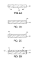
- FIGS. 2A-2K illustrate a first example of a method to produce a device as described above.
- FIG. 2A One commences ( FIG. 2A ) with a substrate 100 which may consist of one of the materials previously mentioned above. If applicable, alignment marks 99 , 99 ′ may be made in rear face 100 ′ of this substrate, where this rear face is defined as the face opposite the one on which the various deposition operations are to be accomplished. The role of these alignment marks will be explained below. These alignment marks can also be made at a later stage.
- an insulating layer 101 ( FIG. 2B ), for example made of silicon dioxide SiO2, or of another material with a low dielectric constant (for example, lower than 5), is deposited or made to grow.
- This insulating layer enables future lower electrode 102 of substrate 100 to be insulated.
- this insulating layer can be structured (for example by chemical or plasma etching), in order subsequently to, for example, bring lower electrode 102 and substrate 100 into contact.
- One or more openings 101 ′ are then formed in layer 101 , one or more of which may emerge in the surface of substrate 100 on which layer 101 has been deposited.
- a lower electrode layer 102 made for example of polycrystalline silicon, or of doped amorphous silicon, or of polycrystalline or amorphous germanium, or more generally, in a semi-conductor material, possibly doped, or more generally of a conducting material, is then deposited on layer 101 ( FIG. 2D ).
- a semi-conductor material possibly doped, or more generally of a conducting material.
- Another particular example is N or P doped polysilicon. Selecting a semi-conductor material for this layer 102 makes it possible to implement molecular bonding.
- This layer 102 is, for example, between 100 nm and 5 ⁇ m or 10 ⁇ m thick.
- a deposition technique can be chosen from one of the following techniques: LPCVD, PECVD, MBD, or others.
- this electrode layer has previously been structured the material constituting this electrode layer reaches, through openings 101 ′, the surface of substrate 100 , thus forming a contact 104 with the latter.
- This contact 104 enables certain elements of the device to be earthed; rear face 100 ′ of substrate 100 may also be earthed.
- Layer 102 may possibly, as illustrated in FIG. 2D , be structured, by formation of a cavity 102 ′, for example by etching, where this etching is stopped at insulating layer 101 .
- This structuring of the lower electrode enables certain portions to be insulated from one another. If one has commenced with an SOI substrate ( FIG. 4 ), cavities 101 ′ will have been obtained by etching of dielectric layer 11 from rear face 10 ′. The next step is the deposition of an insulating layer 103 , the thickness of which will enable the distance separating electrode 102 from substrate 200 to be defined (and therefore the distance separating this electrode from future moving portion 210 ), when the latter has been attached to first substrate 100 .
- This layer is, for example, made of an oxide such as silicon oxide (again, for example: TEOS oxide). It can also be of the order of several hundred nanometers thick, for example between 50 nm and 500 nm or 1 ⁇ m.
- This insulating layer 103 can be deposited only on lower electrode 102 , as illustrated in FIG. 2E or only on substrate 200 , or partly on lower electrode 102 and partly on substrate 200 (as can be seen in FIG. 2G , with layers 103 and 201 ). Whichever possibility is chosen, this insulating layer will form a sacrificial layer which will be etched to release oscillating mass 210 , as explained below.
- the material of insulating layer 103 also fills portions 102 ′ structured or etched in layer 102 , and comes into contact with the upper surface of insulating layer 101 . Certain portions of lower electrode 102 may be insulated by this insulating layer 103 .
- a cavity 109 may possibly, as illustrated in FIG. 2F , be etched in insulating layer 103 and in electrode layer 102 , the etching being stopped on insulating layer 101 . It is therefore possible to structure layer 103 and possibly layer 102 . Different portions of the lower electrode may be insulated from one another by these cavities 109 and/or by the presence, in this electrode layer, of zones of insulating material 103 , as explained above.
- this substrate 100 prepared in this manner, with a second substrate 200 , preferably made of thick monocrystalline silicon ( FIG. 2G ). It is then the surface of insulating layer 103 which comes into contact with substrate 200 or with a possible insulating layer 201 formed on this substrate 200 ( FIG. 2H ).
- Whether or not layer 103 is structured (in other words: whether or not a cavity 109 is present) direct bonding of both substrates 100 , 200 can be accomplished. This step can be accomplished at ambient temperature, at atmospheric pressure, notably if the sealing is accomplished without any cavity 109 or in a vacuum.
- the process may be completed by a consolidation annealing of the bonding interface (typically at a temperature of 1000° C. to 1200° C. for several hours).
- Substrate 200 can then be thinned ( FIG. 2I ), from its surface opposite the one attached to substrate 100 , for example by a polishing technique. It is then sought to obtain a thickness of between 10 ⁇ m and 100 ⁇ m, notably in the case of an MEMS application.
- the moving portion of the MEMS is then defined in layer 200 ′ (which results from the thinning of substrate 200 ) by etching (for example, plasma etching) of layer 200 ′, with stoppage at insulating layer 201 , 103 , as illustrated in FIG. 2J .
- This step enables vertical channels 210 to be produced, which will define the contour of the moving portions of the MEMS.
- a step of etching of sacrificial layers 201 , 103 , under layer 200 ′ enables the moving portion which has just been defined to be released.
- cavity 103 ′ is formed between moving portion 210 and electrode 102 .
- a particular example of this method which enables a direct bonding interface to be obtained, between SiO2 layer 103 and a SiO2 layer 201 , of satisfactory quality (i.e. the etching speed of which is not different from that of sacrificial layer), is as follows:
- alignment marks 99 , 99 ′ may have been previously formed, for example by etching, in the rear face of substrate 100 .
- FIG. 6 An example of such a device is represented schematically in FIG. 6 .
- Rear face 100 ′ of the substrate, on which marks 99 , 99 ′ are made, is positioned on a “chuck” (or plate) 400 on the surface of which means forming an optical guide 401 are provided.
- These means essentially include optical means such as lenses 403 , 403 ′, and mirrors 402 , 402 ′; they will enable a beam 405 to be guided towards lower face 100 ′ of the substrate, in order to read the positions of marks 99 .
- This device enables the precise positions of the marks generated in the rear face to be located, and therefore the other levels, in the front face, to be aligned relative to these marks.
- any number of substrates may be bonded and thinned, as substrate 200 , and all the levels generated on the front faces of these substrates can be aligned with marks 99 , 99 ′ of the rear face of substrate 100 , or produced taking account of the positions of these marks, as explained above.
- a substrate such as the one obtained on conclusion of the step described above in connection with FIG. 2I .
- This substrate therefore includes at least one lower electrode 102 , one sacrificial layer 103 and one structural layer 200 ′. It may also include one or more zones 101 ′ of contact between electrode 102 and substrate 100 .
- Lower electrode 102 may include one or more zones 102 ′, 109 where portions of the electrode are insulated from one another.
- vias 106 ′ The position of one or more vias 106 ′ is defined beforehand. These vias are then etched in structural layer 200 ′ and insulating layer 103 , with lower electrode 102 then acting as the boundary layer. This etching is preferentially of the plasma type ( FIG. 3A ).
- a layer of conducting material 106 is deposited on the surface, this layer being made, for example, of doped polysilicon, metal, or poly-Ge, etc. ( FIG. 3B ). This material also fills the cavities or via 106 ′.
- This layer can also be either directly structured (and therefore deposited in vias 106 ′, but not on the surface of substrate 200 ′), or eliminated from the surface of substrate 200 ′ by polishing and/or total etching without any resin mask, in which case the material present in via 106 ′ is the only material which remains.
- a new layer of conducting material 107 which can be of a nature different from the material of layer 106 , is deposited on layer 200 ′, and then structured, for example by etching. This step enables the locations of the future weld beads to be defined with the cap of the device. At least one of these beads is placed in contact with material 106 used to fill at least one of vias 106 ′. The thickness of these beads 107 will define the distance between the upper surface of moving portion 210 and upper electrode 302 . As a variant, it is possible to have all or a proportion of beads 107 formed beforehand on upper electrode 302 , and not on substrate 200 ′.
- moving structure 210 The steps of definition of moving structure 210 are then implemented, followed by those of etching of sacrificial layer 103 ( FIGS. 3D and 3E ), as previously described above.
- a cap on a surface of which a layer 302 of conducting material has been deposited and structured.
- This layer 302 is made of a metal material or of a metal alloy such as, for example, AlCu, AuSn, AlSI or AuGe, etc. ( FIG. 3F ). Beads 107 may possibly be formed on this conducting layer 302 .
- Both substrates are then sealed hermetically, for example by eutectic sealing or by thermocompression, in a vacuum or in a controlled atmosphere.
- Layer 302 can then come into contact with sealing bead 107 , so as to be positioned opposite moving portion 210 , which is then positioned between two electrodes 102 , 302 .
- the beads are brought on to layer 200 ′, one of them being positioned in contact with the material for filling via 106 ′.
- the structure of FIG. 1 is then obtained.
- Layer 302 then also has a hermetic sealing function, enabling a satisfactory level of vacuum to be obtained in the sealed cavity.
- a contact between upper 302 and lower 102 electrodes is also made.
- the two substrates 100 , 300 are preferably sealed in a vacuum or controlled atmosphere, in order to keep the same level of vacuum in the cavity as in the enclosure in which the sealing is accomplished.
- the resonant frequency (and therefore the system's response) depends on the level of vacuum in the cavity, and the control of the atmosphere (i.e. of the pressure) in the latter enables this frequency to be set. In order to obtain a determined frequency, a determined pressure is set.
- the hermetic sealing also enables moving portion 210 of the device to be protected against the ambient atmosphere.
- the device is then ready to detect a movement of moving portion 210 , this movement taking place outside the plane of the device, i.e. essentially in direction z.
- the movement of the moving portion may also have a component in a plane parallel to the device's main plane, and therefore perpendicular to Z.
- Detection is also accomplished by capacitive electrodes 102 , 302 .
- the signal obtained may be transmitted to data processing and data storage means, which are not represented in the figures.
- Cap substrate 300 may be, for example, a CMOS substrate.
- the last structured metal level (made, for example, of AlCu, or AlSi etc.) of this substrate may be used as an upper electrode 302 and as a hermetic sealing layer.
- the invention is not restricted to the production of MEMs components with capacitive electrodes; it may apply to any structure including only one buried lower electrode.
- the above method, with the formation of 2 electrodes 102 , 302 can be modified and simplified in order to obtain a device with a single electrode.
- material 302 need merely not be deposited on substrate 300 .
- material 302 is deposited only above certain sealing beads 107 a , 107 b , as in FIG. 3G .
- a device with only one lower electrode may also detect a movement of the moving portion in axis z, but in a less sensitive manner.
- molecular bonding makes it possible to hermetically seal the device, which allows a mobile structure to work in a controlled vacuum or a controlled atmosphere; it is the case in particular for a gyroscope.
- Molecular bonding involves a high thermal budget or a high temperature (for example between 900° C. and 1200° C.; typically 1100° C. for a SiO2-SiO2 bonding).
- the materials which are assembled are therefore preferably semi-conductor materials, which are compatible with such a high thermal budget or temperature; in particular the lower electrode is advantageously doped poly-Si.
- the invention may be applied to the production of inertial micro-system or nano-system components. This is in particular the case in the motor vehicle field, for the formation of accelerometers in airbags, or of gyroscopes for course correction.
- CMUT Capacitive Micromachined Ultrasonic
Landscapes
- Engineering & Computer Science (AREA)
- Physics & Mathematics (AREA)
- General Physics & Mathematics (AREA)
- Microelectronics & Electronic Packaging (AREA)
- Manufacturing & Machinery (AREA)
- Radar, Positioning & Navigation (AREA)
- Remote Sensing (AREA)
- Computer Hardware Design (AREA)
- Micromachines (AREA)
- Pressure Sensors (AREA)
- Gyroscopes (AREA)
Abstract
Description
-
- a first substrate, having at least one lower electrode, and a dielectric layer, positioned between the lower electrode and the first substrate; this first substrate, or lower substrate, can be, for example, made of a monocrystalline or polycrystalline semiconducting material, or it has an SOI substrate, or has several stacked materials;
- an intermediate substrate having a moving portion, attached, outside the moving portion, by molecular bonding, or direct bonding, with the first substrate, where the moving portion is facing at least a portion of the lower electrode,
- an upper substrate, attached to the intermediate substrate, for example of the CMOS type, where the said moving portion can be made to move between the lower electrode and the upper substrate.
-
- forming a first substrate, including at least one electrode, called the lower electrode, and a first dielectric layer,
- then followed by assembling, by molecular bonding, an intermediate substrate, with the first substrate,
- the assembling step being then followed by producing a moving portion in the intermediate substrate,
- this step of producing a moving portion being then followed by forming a cavity in the first dielectric layer, at least under the moving portion, such that the moving portion is facing at least a portion of the lower electrode,
- the cavity forming step being then followed by assembly of a substrate, called the upper substrate, with the intermediate substrate, such that the said moving portion can be made to move between the lower electrode and the upper substrate, at least in a direction perpendicular to this lower electrode and, possibly, in a plane parallel to the main plane or to this lower electrode. The electrode or electrodes therefore enable the component, perpendicular to the main plane of the device, of the movement of the moving portion to be initiated or detected, with the understanding that this movement of the moving portion can have other components, particularly in a plane parallel to this main plane.
-
- The upper substrate may be fixed securely to the intermediate substrate by means of a sealing bead;
- and/or means can be provided to form an electrical contact between the lower electrode and the upper electrode and/or means can be provided to form an electrical contact between the lower electrode and the first substrate;
- and/or the intermediate substrate is made from monocrystalline silicon;
- and/or the upper substrate is fixed securely to the intermediate substrate hermetically and/or using a sealing bead and/or by eutectic sealing or by thermocompression using the sealing bead.
-
- a densification of this
layer 103, for example by oxidisation at a temperature close to the bonding temperature (for example 1050° C.), in order that all the layers have a thermal budget similar to that of the bonding (this stage notably allows the layers to be degassed). This step of densification enables the same density oflayers - and/or polishing of
layer 103, which enables a very flat surface to be obtained for the molecular sealing.
- a densification of this
-
- Deposition of
lower electrode layer 102, for example of N or P doped polysilicon of between 100 nm and several microns thick (FIGS. 2A-2D ), - Deposition of a
dielectric layer 103, for example TEOS oxide, of the order of several hundred nanometers thick (FIG. 2E ), - Complete densification of this
oxide layer 103, for example by oxidisation at a temperature close to the bonding temperature (for example 1050° C.), in order that all the layers have a thermal budget similar to that of the bonding (through the effect of degassing of the layers). - Polishing of
oxide 103 before molecular bonding, enabling a perfectly flat surface to be obtained for the molecular sealing, - Structuring, or not, of
layers - Direct bonding at ambient temperature, at atmospheric pressure, if the sealing is accomplished without a cavity or in a vacuum.
- Consolidation annealing of the bonding interface between both
substrates - Thinning of
substrate 200 until the thickness sought for the moving portion is reached: between 10 μm and 100 μm for an MEMS application, where this thinning ofsubstrate 200 may be accomplished by “grinding” and/or polishing, - definition of the moving portion in
layer 200′ by etching of the latter, for example by a plasma technique, with stoppage at insulatinglayer - release of the moving portion, by etching of
sacrificial layers
- Deposition of
-
- the contacts with a view to measuring the voltages detected in the electrodes may be made through
substrate 100 and/or throughcap substrate 300; - and/or the upper electrode and/or the lower electrode may be etched such that they are not within the sealing zones.
- the contacts with a view to measuring the voltages detected in the electrodes may be made through
Claims (13)
Applications Claiming Priority (2)
| Application Number | Priority Date | Filing Date | Title |
|---|---|---|---|
| FR1156351A FR2977885A1 (en) | 2011-07-12 | 2011-07-12 | METHOD FOR PRODUCING A DIRECT-REPORT BURNED ELECTRODE STRUCTURE AND STRUCTURE THUS OBTAINED |
| FR1156351 | 2011-07-12 |
Publications (2)
| Publication Number | Publication Date |
|---|---|
| US20130175643A1 US20130175643A1 (en) | 2013-07-11 |
| US8692337B2 true US8692337B2 (en) | 2014-04-08 |
Family
ID=46420029
Family Applications (1)
| Application Number | Title | Priority Date | Filing Date |
|---|---|---|---|
| US13/546,751 Active US8692337B2 (en) | 2011-07-12 | 2012-07-11 | Structure with a moving portion and a buried electrode for movement detection included in a multi-substrate configuration |
Country Status (5)
| Country | Link |
|---|---|
| US (1) | US8692337B2 (en) |
| EP (1) | EP2546189B1 (en) |
| JP (1) | JP2013018114A (en) |
| CN (1) | CN102874737A (en) |
| FR (1) | FR2977885A1 (en) |
Cited By (10)
| Publication number | Priority date | Publication date | Assignee | Title |
|---|---|---|---|---|
| US20130144542A1 (en) * | 2010-06-07 | 2013-06-06 | California Institute Of Technology | Analysis device including a mems and/or nems network |
| US20140084349A1 (en) * | 2012-09-24 | 2014-03-27 | Robert Bosch Gmbh | Microelectronic Component and Corresponding Production Process |
| US20140151721A1 (en) * | 2012-11-30 | 2014-06-05 | Corning Incorporated | Phase transition cooling in led lighting devices |
| US20140264644A1 (en) * | 2013-03-12 | 2014-09-18 | Taiwan Semiconductor Manufacturing Company, Ltd. | MEMS Method and Structure |
| US20150175407A1 (en) * | 2013-12-20 | 2015-06-25 | Taiwan Semiconductor Manufacturing Company, Ltd. | Micro electromechanical system sensor and method of forming the same |
| US9234879B2 (en) * | 2013-07-22 | 2016-01-12 | Commissariat à l'énergie atomique et aux énergies alternatives | Device comprising a fluid channel provided with at least one micro or nanoelectronic system and method for carrying out such a device |
| US20180240908A1 (en) * | 2009-12-28 | 2018-08-23 | Sony Corporation | Semiconductor component and manufacturing method thereof |
| US20190115346A1 (en) * | 2017-10-13 | 2019-04-18 | Globalfoundries Inc. | Cut inside replacement metal gate trench to mitigate n-p proximity effect |
| US10643884B2 (en) | 2015-08-12 | 2020-05-05 | Commissariat A L'energie Atomique Et Aux Energies Alternatives | Method for manufacturing a semiconductor structure with temporary direct bonding using a porous layer |
| US10833008B2 (en) * | 2017-03-15 | 2020-11-10 | Amkor Technology Singapore Holding Pte. Ltd. | Method of forming a packaged semiconductor device using ganged conductive connective assembly and structure |
Families Citing this family (25)
| Publication number | Priority date | Publication date | Assignee | Title |
|---|---|---|---|---|
| US8564076B1 (en) * | 2013-01-30 | 2013-10-22 | Invensense, Inc. | Internal electrical contact for enclosed MEMS devices |
| US9533873B2 (en) | 2013-02-05 | 2017-01-03 | Butterfly Network, Inc. | CMOS ultrasonic transducers and related apparatus and methods |
| US9079761B2 (en) * | 2013-03-14 | 2015-07-14 | Taiwan Semiconductor Manufacturing Company, Ltd. | Stacked semiconductor device and method of forming the same related cases |
| CN103193197B (en) * | 2013-04-02 | 2016-04-06 | 厦门大学 | A kind of micro element movable structure preparation method based on silicon/glass anode linkage |
| DE102013208814A1 (en) * | 2013-05-14 | 2014-11-20 | Robert Bosch Gmbh | Integrated yaw rate and acceleration sensor and method of manufacturing an integrated yaw rate and acceleration sensor |
| US20140348513A1 (en) * | 2013-05-24 | 2014-11-27 | Alcatel-Lucent Usa, Inc. | Optical assembly for optical communication systems |
| CN104249991B (en) * | 2013-06-26 | 2016-08-10 | 中芯国际集成电路制造(上海)有限公司 | MEMS and preparation method thereof |
| CN104340951B (en) * | 2013-07-30 | 2016-12-28 | 中芯国际集成电路制造(上海)有限公司 | A kind of preparation method of motion sensor |
| CN104445049B (en) * | 2013-09-24 | 2016-08-03 | 中芯国际集成电路制造(上海)有限公司 | MEMS forming method |
| US9487391B2 (en) * | 2013-11-19 | 2016-11-08 | Taiwan Semiconductor Manufacturing Co., Ltd. | Micro-electro mechanical system (MEMS) device having a blocking layer formed between closed chamber and a dielectric layer of a CMOS substrate |
| US9422156B2 (en) * | 2014-07-07 | 2016-08-23 | Invensense, Inc. | Integrated CMOS and MEMS sensor fabrication method and structure |
| US9067779B1 (en) * | 2014-07-14 | 2015-06-30 | Butterfly Network, Inc. | Microfabricated ultrasonic transducers and related apparatus and methods |
| CN105819393B (en) * | 2015-01-06 | 2017-04-05 | 中芯国际集成电路制造(上海)有限公司 | The method for improving metal loss in inertial sensor |
| FI127042B (en) | 2015-09-09 | 2017-10-13 | Murata Manufacturing Co | An electrode for a microelectromechanical device |
| US10509006B2 (en) * | 2016-06-20 | 2019-12-17 | Axbio Inc. | Devices and methods for measuring the properties of macromolecules |
| DE102017200725A1 (en) * | 2017-01-18 | 2018-07-19 | Robert Bosch Gmbh | Micromechanical sensor |
| US10196261B2 (en) | 2017-03-08 | 2019-02-05 | Butterfly Network, Inc. | Microfabricated ultrasonic transducers and related apparatus and methods |
| US10793427B2 (en) * | 2017-04-04 | 2020-10-06 | Kionix, Inc. | Eutectic bonding with AlGe |
| US10512936B2 (en) | 2017-06-21 | 2019-12-24 | Butterfly Network, Inc. | Microfabricated ultrasonic transducer having individual cells with electrically isolated electrode sections |
| DE102017213636A1 (en) | 2017-08-07 | 2019-02-07 | Robert Bosch Gmbh | Process for the production of thin MEMS chips on SOI substrate and micromechanical device |
| JP7073876B2 (en) * | 2018-04-16 | 2022-05-24 | 株式会社デンソー | Semiconductor devices and their manufacturing methods |
| US11313877B2 (en) | 2018-06-19 | 2022-04-26 | Kionix, Inc. | Near-zero power wakeup electro-mechanical system |
| CN109470228B (en) * | 2018-10-30 | 2020-12-08 | 北京时代民芯科技有限公司 | A kind of MEMS dish gyroscope based on embedded differential electrode and preparation method thereof |
| FR3088480B1 (en) | 2018-11-09 | 2020-12-04 | Commissariat Energie Atomique | BONDING PROCESS WITH ELECTRONICALLY STIMULATED DESORPTION |
| CN112151312B (en) * | 2020-10-13 | 2023-04-07 | 深圳清华大学研究院 | Electrode switch based on structure is super smooth |
Citations (30)
| Publication number | Priority date | Publication date | Assignee | Title |
|---|---|---|---|---|
| US20030001221A1 (en) | 2001-02-03 | 2003-01-02 | Frank Fischer | Micromechanical component as well as a method for producing a micromechanical component |
| US20030093895A1 (en) * | 2001-04-26 | 2003-05-22 | Masaru Miyazaki | Connecting member, a micro-switch, a method for manufacturing a connecting member, and a method for manufacturing a micro-switch |
| US6661069B1 (en) * | 2002-10-22 | 2003-12-09 | International Business Machines Corporation | Micro-electromechanical varactor with enhanced tuning range |
| US6761068B1 (en) | 1998-09-29 | 2004-07-13 | Fraunhofer-Gesellschaft Zur Foerderung Der Angewandten Forschung, E.V. | Micromechanical rotation rate sensor and method for producing the same |
| US7083997B2 (en) | 2000-08-03 | 2006-08-01 | Analog Devices, Inc. | Bonded wafer optical MEMS process |
| US20060208326A1 (en) | 2005-03-18 | 2006-09-21 | Nasiri Steven S | Method of fabrication of ai/ge bonding in a wafer packaging environment and a product produced therefrom |
| US7180019B1 (en) * | 2006-06-26 | 2007-02-20 | Temic Automotive Of North America, Inc. | Capacitive accelerometer or acceleration switch |
| US7192001B2 (en) * | 2003-05-08 | 2007-03-20 | The Regents Of The University Of Michigan Office Of Technology Transfer | Thermopneumatic microvalve |
| US20070090474A1 (en) | 2005-09-08 | 2007-04-26 | Li Gary G | MEMS device and method of fabrication |
| US20070113661A1 (en) | 2005-11-11 | 2007-05-24 | Hubert Benzel | Sensor system and method for manufacturing a sensor system |
| WO2007135878A1 (en) | 2006-05-18 | 2007-11-29 | Semiconductor Energy Laboratory Co., Ltd. | Microstructure, micromachine, and manufacturing method of microstructure and micromachine |
| US7528691B2 (en) * | 2005-08-26 | 2009-05-05 | Innovative Micro Technology | Dual substrate electrostatic MEMS switch with hermetic seal and method of manufacture |
| US20090297770A1 (en) * | 2007-08-10 | 2009-12-03 | Murata Manufacturing Co., Ltd. | Element structure and method for producing the same |
| FR2932789A1 (en) | 2008-06-23 | 2009-12-25 | Commissariat Energie Atomique | METHOD FOR MANUFACTURING AN ELECTROMECHANICAL STRUCTURE COMPRISING AT LEAST ONE MECHANICAL REINFORCING PILLAR |
| US20100019388A1 (en) | 1992-07-28 | 2010-01-28 | Micron Technology, Inc. | Method for an integrated circuit contact |
| WO2010081603A1 (en) | 2009-01-15 | 2010-07-22 | Austriamicrosystems Ag | Semiconductor circuit having interlayer connections and method for producing vertically integrated circuits |
| US20100193884A1 (en) * | 2009-02-02 | 2010-08-05 | Woo Tae Park | Method of Fabricating High Aspect Ratio Transducer Using Metal Compression Bonding |
| US7859091B2 (en) * | 2007-02-22 | 2010-12-28 | Denso Corporation | Manufacturing methods for semiconductor device with sealed cap |
| US20110012247A1 (en) * | 2009-07-15 | 2011-01-20 | Taiwan Semiconductor Manufacturing Company, Ltd. | Socket type mems bonding |
| US7893798B2 (en) * | 2007-05-09 | 2011-02-22 | Innovative Micro Technology | Dual substrate MEMS plate switch and method of manufacture |
| US7950288B2 (en) | 2006-06-13 | 2011-05-31 | Denso Corporation | Physical quantity sensor |
| US20110156106A1 (en) * | 2009-12-28 | 2011-06-30 | Solid State System Co., Ltd. | Hermetic mems device and method for fabricating hermetic mems device and package structure of mems device |
| US20120001277A1 (en) | 2010-06-30 | 2012-01-05 | Woo Tae Park | Methods for making in-plane and out-of-plane sensing micro-electro-mechanical systems (mems) |
| US8193550B2 (en) * | 2003-04-08 | 2012-06-05 | Stmicroelectronics S.R.L. | Method for manufacturing a micro-electro-mechanical device, in particular an optical microswitch, and micro-electro-mechanical device thus obtained |
| US8267583B2 (en) * | 2009-10-19 | 2012-09-18 | Oracle America, Inc. | Three-dimensional macro-chip including optical interconnects |
| US8269290B2 (en) * | 2008-09-15 | 2012-09-18 | Denso Corporation | Semiconductor device including a plurality of semiconductor substrates and method of manufacturing the same |
| US20120248615A1 (en) * | 2011-03-28 | 2012-10-04 | Miradia, Inc. | Mems device and manufacturing process thereof |
| US8318526B2 (en) * | 2010-08-09 | 2012-11-27 | Memsor Corporation | Manufacturing method for light-sensing structure |
| US20120313235A1 (en) * | 2011-06-10 | 2012-12-13 | Taiwan Semiconductor Manufacturing Company, Ltd. | Semiconductor Devices With Moving Members and Methods for Making the Same |
| US20130076202A1 (en) * | 2010-07-16 | 2013-03-28 | Yasuyuki Naito | Micro-electromechanical generator and electric apparatus using same |
Family Cites Families (6)
| Publication number | Priority date | Publication date | Assignee | Title |
|---|---|---|---|---|
| GB0320405D0 (en) * | 2003-08-30 | 2003-10-01 | Qinetiq Ltd | Micro electromechanical system switch |
| US7944599B2 (en) * | 2004-09-27 | 2011-05-17 | Qualcomm Mems Technologies, Inc. | Electromechanical device with optical function separated from mechanical and electrical function |
| US20070236307A1 (en) * | 2006-04-10 | 2007-10-11 | Lianjun Liu | Methods and apparatus for a packaged MEMS switch |
| CN101164863B (en) * | 2006-10-20 | 2012-06-13 | 精工爱普生株式会社 | Mems device and fabrication method thereof |
| JP5260342B2 (en) * | 2009-01-30 | 2013-08-14 | ローム株式会社 | MEMS sensor |
| JP2011011325A (en) * | 2009-07-06 | 2011-01-20 | Murata Mfg Co Ltd | Mems element |
-
2011
- 2011-07-12 FR FR1156351A patent/FR2977885A1/en not_active Withdrawn
-
2012
- 2012-07-10 EP EP12175740.5A patent/EP2546189B1/en active Active
- 2012-07-11 JP JP2012155321A patent/JP2013018114A/en active Pending
- 2012-07-11 US US13/546,751 patent/US8692337B2/en active Active
- 2012-07-12 CN CN201210242505XA patent/CN102874737A/en active Pending
Patent Citations (32)
| Publication number | Priority date | Publication date | Assignee | Title |
|---|---|---|---|---|
| US20100019388A1 (en) | 1992-07-28 | 2010-01-28 | Micron Technology, Inc. | Method for an integrated circuit contact |
| US6761068B1 (en) | 1998-09-29 | 2004-07-13 | Fraunhofer-Gesellschaft Zur Foerderung Der Angewandten Forschung, E.V. | Micromechanical rotation rate sensor and method for producing the same |
| US7083997B2 (en) | 2000-08-03 | 2006-08-01 | Analog Devices, Inc. | Bonded wafer optical MEMS process |
| US20030001221A1 (en) | 2001-02-03 | 2003-01-02 | Frank Fischer | Micromechanical component as well as a method for producing a micromechanical component |
| US20030093895A1 (en) * | 2001-04-26 | 2003-05-22 | Masaru Miyazaki | Connecting member, a micro-switch, a method for manufacturing a connecting member, and a method for manufacturing a micro-switch |
| US6661069B1 (en) * | 2002-10-22 | 2003-12-09 | International Business Machines Corporation | Micro-electromechanical varactor with enhanced tuning range |
| US8193550B2 (en) * | 2003-04-08 | 2012-06-05 | Stmicroelectronics S.R.L. | Method for manufacturing a micro-electro-mechanical device, in particular an optical microswitch, and micro-electro-mechanical device thus obtained |
| US7192001B2 (en) * | 2003-05-08 | 2007-03-20 | The Regents Of The University Of Michigan Office Of Technology Transfer | Thermopneumatic microvalve |
| US20060208326A1 (en) | 2005-03-18 | 2006-09-21 | Nasiri Steven S | Method of fabrication of ai/ge bonding in a wafer packaging environment and a product produced therefrom |
| US7528691B2 (en) * | 2005-08-26 | 2009-05-05 | Innovative Micro Technology | Dual substrate electrostatic MEMS switch with hermetic seal and method of manufacture |
| US20070090474A1 (en) | 2005-09-08 | 2007-04-26 | Li Gary G | MEMS device and method of fabrication |
| US20070113661A1 (en) | 2005-11-11 | 2007-05-24 | Hubert Benzel | Sensor system and method for manufacturing a sensor system |
| WO2007135878A1 (en) | 2006-05-18 | 2007-11-29 | Semiconductor Energy Laboratory Co., Ltd. | Microstructure, micromachine, and manufacturing method of microstructure and micromachine |
| US20080176046A1 (en) | 2006-05-18 | 2008-07-24 | Semiconductor Energy Laboratory Co., Ltd. | Microstructure, micromachine, and manufacturing method of microstructure and micromachine |
| US7950288B2 (en) | 2006-06-13 | 2011-05-31 | Denso Corporation | Physical quantity sensor |
| US7180019B1 (en) * | 2006-06-26 | 2007-02-20 | Temic Automotive Of North America, Inc. | Capacitive accelerometer or acceleration switch |
| US7859091B2 (en) * | 2007-02-22 | 2010-12-28 | Denso Corporation | Manufacturing methods for semiconductor device with sealed cap |
| US7893798B2 (en) * | 2007-05-09 | 2011-02-22 | Innovative Micro Technology | Dual substrate MEMS plate switch and method of manufacture |
| US20090297770A1 (en) * | 2007-08-10 | 2009-12-03 | Murata Manufacturing Co., Ltd. | Element structure and method for producing the same |
| US20090321887A1 (en) | 2008-06-23 | 2009-12-31 | Commissariat A L'energie Atomique | Method of fabricating an electromechanical structure including at least one mechanical reinforcing pillar |
| FR2932789A1 (en) | 2008-06-23 | 2009-12-25 | Commissariat Energie Atomique | METHOD FOR MANUFACTURING AN ELECTROMECHANICAL STRUCTURE COMPRISING AT LEAST ONE MECHANICAL REINFORCING PILLAR |
| US8269290B2 (en) * | 2008-09-15 | 2012-09-18 | Denso Corporation | Semiconductor device including a plurality of semiconductor substrates and method of manufacturing the same |
| WO2010081603A1 (en) | 2009-01-15 | 2010-07-22 | Austriamicrosystems Ag | Semiconductor circuit having interlayer connections and method for producing vertically integrated circuits |
| US20100193884A1 (en) * | 2009-02-02 | 2010-08-05 | Woo Tae Park | Method of Fabricating High Aspect Ratio Transducer Using Metal Compression Bonding |
| US20110012247A1 (en) * | 2009-07-15 | 2011-01-20 | Taiwan Semiconductor Manufacturing Company, Ltd. | Socket type mems bonding |
| US8267583B2 (en) * | 2009-10-19 | 2012-09-18 | Oracle America, Inc. | Three-dimensional macro-chip including optical interconnects |
| US20110156106A1 (en) * | 2009-12-28 | 2011-06-30 | Solid State System Co., Ltd. | Hermetic mems device and method for fabricating hermetic mems device and package structure of mems device |
| US20120001277A1 (en) | 2010-06-30 | 2012-01-05 | Woo Tae Park | Methods for making in-plane and out-of-plane sensing micro-electro-mechanical systems (mems) |
| US20130076202A1 (en) * | 2010-07-16 | 2013-03-28 | Yasuyuki Naito | Micro-electromechanical generator and electric apparatus using same |
| US8318526B2 (en) * | 2010-08-09 | 2012-11-27 | Memsor Corporation | Manufacturing method for light-sensing structure |
| US20120248615A1 (en) * | 2011-03-28 | 2012-10-04 | Miradia, Inc. | Mems device and manufacturing process thereof |
| US20120313235A1 (en) * | 2011-06-10 | 2012-12-13 | Taiwan Semiconductor Manufacturing Company, Ltd. | Semiconductor Devices With Moving Members and Methods for Making the Same |
Non-Patent Citations (8)
| Title |
|---|
| Andreas Plöbetal, et al., "Wafer direct bonding: tailoring adhesion between brittle materials", Materials Science and Engineering, vol. R25, No. 1-2, XP 004167445, Mar. 10, 1999, pp. 1-88. |
| Andreas Plöβl, et al., "Wafer direct bonding: tailoring adhesion between brittle materials", Materials Science and Engineering, vol. R25, No. 1-2, XP 004167445, Mar. 10, 1999, pp. 1-88. |
| Anu Kärkkäinen, et al., "Optimized Design and Process for Making a DC Voltage Reference Based on MEMS", IEEE Transactions on Instrumentation and Measurement, vol. 54, No. 2, XP 011128181, Apr. 2005, pp. 563-566. |
| French Preliminary Search Report issued Jan. 24, 2012, in Patent Application No. 1156351 (with English Translation of Category of Cited Documents). |
| Q. -Y. Tong, "Principles of wafer bonding", INSPEC, Chapter 1, 2002, pp. 1-20. |
| T. Yamamoto, et al., "Capacitive Accelerometer with High Aspect Ratio single crystalline Silicon Microstructure Using the SOI Structure with Polysilicon-Based Interconnect technique", Proceedings of the IEEE 13th Annual International Conference on Micro Electro Mechanical Systems MEMS, XP 001045369, Jan. 23, 2000, pp. 514-519. |
| U.S. Appl. No. 13/546,411, filed Jul. 11, 2012, Giroud, et al. |
| Yogesh B. Gianchandani, et al., "Impact of Long, High Temperature Anneals on Residual Stress in Polysilicon", Transducers, IEEE International Conference on Solid-State Sensors and Actuators, Jun. 16-19, 1997, pp. 623-624. |
Cited By (25)
| Publication number | Priority date | Publication date | Assignee | Title |
|---|---|---|---|---|
| US11848380B2 (en) | 2009-12-28 | 2023-12-19 | Sony Group Corporation | Semiconductor component and manufacturing method thereof |
| US20180240908A1 (en) * | 2009-12-28 | 2018-08-23 | Sony Corporation | Semiconductor component and manufacturing method thereof |
| US11043590B2 (en) | 2009-12-28 | 2021-06-22 | Sony Corporation | Semiconductor component and manufacturing method thereof |
| US10727335B2 (en) * | 2009-12-28 | 2020-07-28 | Sony Corporation | Semiconductor component and manufacturing method thereof |
| US20130144542A1 (en) * | 2010-06-07 | 2013-06-06 | California Institute Of Technology | Analysis device including a mems and/or nems network |
| US10216698B2 (en) * | 2010-06-07 | 2019-02-26 | Commissariat à l 'Energie Atomique et aux Energies Alternatives | Analysis device including a MEMS and/or NEMS network |
| US9082882B2 (en) * | 2012-09-24 | 2015-07-14 | Robert Bosch Gmbh | Microelectronic component and corresponding production process |
| US20140084349A1 (en) * | 2012-09-24 | 2014-03-27 | Robert Bosch Gmbh | Microelectronic Component and Corresponding Production Process |
| US20140151721A1 (en) * | 2012-11-30 | 2014-06-05 | Corning Incorporated | Phase transition cooling in led lighting devices |
| US20140264644A1 (en) * | 2013-03-12 | 2014-09-18 | Taiwan Semiconductor Manufacturing Company, Ltd. | MEMS Method and Structure |
| US9394164B2 (en) * | 2013-03-12 | 2016-07-19 | Taiwan Semiconductor Manufacturing Company, Ltd. | MEMS method and structure |
| US20160325988A1 (en) * | 2013-03-12 | 2016-11-10 | Taiwan Semiconductor Manufacturing Company, Ltd. | MEMS Method and Structure |
| US10889493B2 (en) * | 2013-03-12 | 2021-01-12 | Taiwan Semiconductor Manufacturing Company, Ltd. | MEMS method and structure |
| US10160642B2 (en) * | 2013-03-12 | 2018-12-25 | Taiwan Semiconductor Manufacturing Company, Ltd. | MEMS method and structure |
| US9234879B2 (en) * | 2013-07-22 | 2016-01-12 | Commissariat à l'énergie atomique et aux énergies alternatives | Device comprising a fluid channel provided with at least one micro or nanoelectronic system and method for carrying out such a device |
| US10384933B2 (en) * | 2013-12-20 | 2019-08-20 | Taiwan Semiconductor Manufacturing Company, Ltd. | Method of forming micro electromechanical system sensor |
| US20170313581A1 (en) * | 2013-12-20 | 2017-11-02 | Taiwan Semiconductor Manufacturing Company, Ltd. | Method of forming micro electromechanical system sensor |
| US11014805B2 (en) | 2013-12-20 | 2021-05-25 | Taiwan Semiconductor Manufacturing Company, Ltd. | Method of forming semiconductor package and semiconductor package |
| US9725310B2 (en) * | 2013-12-20 | 2017-08-08 | Taiwan Semiconductor Manufacturing Company, Ltd. | Micro electromechanical system sensor and method of forming the same |
| US20150175407A1 (en) * | 2013-12-20 | 2015-06-25 | Taiwan Semiconductor Manufacturing Company, Ltd. | Micro electromechanical system sensor and method of forming the same |
| US10643884B2 (en) | 2015-08-12 | 2020-05-05 | Commissariat A L'energie Atomique Et Aux Energies Alternatives | Method for manufacturing a semiconductor structure with temporary direct bonding using a porous layer |
| US10833008B2 (en) * | 2017-03-15 | 2020-11-10 | Amkor Technology Singapore Holding Pte. Ltd. | Method of forming a packaged semiconductor device using ganged conductive connective assembly and structure |
| US10446550B2 (en) * | 2017-10-13 | 2019-10-15 | Globalfoundries Inc. | Cut inside replacement metal gate trench to mitigate N-P proximity effect |
| US10658363B2 (en) * | 2017-10-13 | 2020-05-19 | Globalfoundries Inc. | Cut inside replacement metal gate trench to mitigate N-P proximity effect |
| US20190115346A1 (en) * | 2017-10-13 | 2019-04-18 | Globalfoundries Inc. | Cut inside replacement metal gate trench to mitigate n-p proximity effect |
Also Published As
| Publication number | Publication date |
|---|---|
| JP2013018114A (en) | 2013-01-31 |
| EP2546189A1 (en) | 2013-01-16 |
| EP2546189B1 (en) | 2020-02-12 |
| CN102874737A (en) | 2013-01-16 |
| FR2977885A1 (en) | 2013-01-18 |
| US20130175643A1 (en) | 2013-07-11 |
Similar Documents
| Publication | Publication Date | Title |
|---|---|---|
| US8692337B2 (en) | Structure with a moving portion and a buried electrode for movement detection included in a multi-substrate configuration | |
| US7104129B2 (en) | Vertically integrated MEMS structure with electronics in a hermetically sealed cavity | |
| US7247246B2 (en) | Vertical integration of a MEMS structure with electronics in a hermetically sealed cavity | |
| US20100193884A1 (en) | Method of Fabricating High Aspect Ratio Transducer Using Metal Compression Bonding | |
| EP3208231B1 (en) | Method of fabrication of ai/ge bonding in a wafer packaging environment | |
| US7851876B2 (en) | Micro electro mechanical system | |
| US20080237823A1 (en) | Aluminum Based Bonding of Semiconductor Wafers | |
| US20110092018A1 (en) | Wafer level packaged mems device | |
| US12092460B2 (en) | Silicon MEMS gyroscopes with upper and lower sense plates | |
| US9051172B2 (en) | Method for manufacturing a hermetically sealed structure | |
| CN110668394B (en) | Preparation method of anti-interference overload-resistant MEMS accelerometer | |
| US11161734B2 (en) | MEMS assembly and manufacturing method thereof | |
| Graham et al. | A method for wafer-scale encapsulation of large lateral deflection MEMS devices | |
| CN101254894A (en) | Encapsulated micro mobile device and method of manufacturing the same | |
| JP6305647B2 (en) | Method for manufacturing electromechanical devices and corresponding devices | |
| JP7129599B2 (en) | sensor | |
| Li et al. | Silicon-Glass-Silicon Triple Stacked Structure for Fabrication of MEMS Resonator Accelerometer | |
| US11981560B2 (en) | Stress-isolated MEMS device comprising substrate having cavity and method of manufacture | |
| Vukasin et al. | Etch-hole free, large gap wafer scale encapsulation process for microelectromechanical resonators | |
| US20170081183A1 (en) | Micromechanical layer system | |
| JP5827365B2 (en) | Method for forming device packaged at wafer level | |
| Sun et al. | Post CMOS integration of high aspect ratio SOI MEMS devices | |
| Du et al. | Chip level packaging for MEMS using silicon cap | |
| Oldsen et al. | Waferlevel Vacuum Packaged Microscanners: A High Yield Fabrication Process for Mobile Applications | |
| JPH11345982A (en) | Manufacture of board having movable parts |
Legal Events
| Date | Code | Title | Description |
|---|---|---|---|
| AS | Assignment |
Owner name: COMMISSARIAT A L'ENERGIE ATOMIQUE ET AUX ENERGIES Free format text: ASSIGNMENT OF ASSIGNORS INTEREST;ASSIGNORS:BERTHELOT, AUDREY;LARREY, VINCENT;POLIZZI, JEAN-PHILIPPE;AND OTHERS;REEL/FRAME:029840/0993 Effective date: 20130122 Owner name: FREESCALE SEMICONDUCTOR INC, TEXAS Free format text: ASSIGNMENT OF ASSIGNORS INTEREST;ASSIGNORS:DESAI, HEMANT;PARK, WOO TAE;REEL/FRAME:029841/0041 Effective date: 20130122 |
|
| AS | Assignment |
Owner name: CITIBANK, N.A., AS NOTES COLLATERAL AGENT, NEW YOR Free format text: SUPPLEMENT TO IP SECURITY AGREEMENT;ASSIGNOR:FREESCALE SEMICONDUCTOR, INC.;REEL/FRAME:030256/0471 Effective date: 20121031 Owner name: CITIBANK, N.A., AS NOTES COLLATERAL AGENT, NEW YOR Free format text: SUPPLEMENT TO IP SECURITY AGREEMENT;ASSIGNOR:FREESCALE SEMICONDUCTOR, INC.;REEL/FRAME:030256/0625 Effective date: 20121031 Owner name: CITIBANK, N.A., AS NOTES COLLATERAL AGENT, NEW YOR Free format text: SUPPLEMENT TO IP SECURITY AGREEMENT;ASSIGNOR:FREESCALE SEMICONDUCTOR, INC.;REEL/FRAME:030256/0544 Effective date: 20121031 |
|
| AS | Assignment |
Owner name: CITIBANK, N.A., AS NOTES COLLATERAL AGENT, NEW YOR Free format text: SECURITY AGREEMENT;ASSIGNOR:FREESCALE SEMICONDUCTOR, INC.;REEL/FRAME:030633/0424 Effective date: 20130521 |
|
| AS | Assignment |
Owner name: CITIBANK, N.A., AS NOTES COLLATERAL AGENT, NEW YOR Free format text: SECURITY AGREEMENT;ASSIGNOR:FREESCALE SEMICONDUCTOR, INC.;REEL/FRAME:031591/0266 Effective date: 20131101 |
|
| STCF | Information on status: patent grant |
Free format text: PATENTED CASE |
|
| AS | Assignment |
Owner name: FREESCALE SEMICONDUCTOR, INC., TEXAS Free format text: PATENT RELEASE;ASSIGNOR:CITIBANK, N.A., AS COLLATERAL AGENT;REEL/FRAME:037357/0633 Effective date: 20151207 Owner name: FREESCALE SEMICONDUCTOR, INC., TEXAS Free format text: PATENT RELEASE;ASSIGNOR:CITIBANK, N.A., AS COLLATERAL AGENT;REEL/FRAME:037357/0614 Effective date: 20151207 Owner name: FREESCALE SEMICONDUCTOR, INC., TEXAS Free format text: PATENT RELEASE;ASSIGNOR:CITIBANK, N.A., AS COLLATERAL AGENT;REEL/FRAME:037357/0652 Effective date: 20151207 |
|
| AS | Assignment |
Owner name: MORGAN STANLEY SENIOR FUNDING, INC., MARYLAND Free format text: ASSIGNMENT AND ASSUMPTION OF SECURITY INTEREST IN PATENTS;ASSIGNOR:CITIBANK, N.A.;REEL/FRAME:037486/0517 Effective date: 20151207 |
|
| AS | Assignment |
Owner name: MORGAN STANLEY SENIOR FUNDING, INC., MARYLAND Free format text: ASSIGNMENT AND ASSUMPTION OF SECURITY INTEREST IN PATENTS;ASSIGNOR:CITIBANK, N.A.;REEL/FRAME:037518/0292 Effective date: 20151207 |
|
| AS | Assignment |
Owner name: MORGAN STANLEY SENIOR FUNDING, INC., MARYLAND Free format text: SECURITY AGREEMENT SUPPLEMENT;ASSIGNOR:NXP B.V.;REEL/FRAME:038017/0058 Effective date: 20160218 |
|
| AS | Assignment |
Owner name: MORGAN STANLEY SENIOR FUNDING, INC., MARYLAND Free format text: CORRECTIVE ASSIGNMENT TO CORRECT THE REMOVE APPLICATION 12092129 PREVIOUSLY RECORDED ON REEL 038017 FRAME 0058. ASSIGNOR(S) HEREBY CONFIRMS THE SECURITY AGREEMENT SUPPLEMENT;ASSIGNOR:NXP B.V.;REEL/FRAME:039361/0212 Effective date: 20160218 |
|
| AS | Assignment |
Owner name: NXP, B.V., F/K/A FREESCALE SEMICONDUCTOR, INC., NETHERLANDS Free format text: RELEASE BY SECURED PARTY;ASSIGNOR:MORGAN STANLEY SENIOR FUNDING, INC.;REEL/FRAME:040925/0001 Effective date: 20160912 Owner name: NXP, B.V., F/K/A FREESCALE SEMICONDUCTOR, INC., NE Free format text: RELEASE BY SECURED PARTY;ASSIGNOR:MORGAN STANLEY SENIOR FUNDING, INC.;REEL/FRAME:040925/0001 Effective date: 20160912 |
|
| AS | Assignment |
Owner name: NXP B.V., NETHERLANDS Free format text: RELEASE BY SECURED PARTY;ASSIGNOR:MORGAN STANLEY SENIOR FUNDING, INC.;REEL/FRAME:040928/0001 Effective date: 20160622 |
|
| AS | Assignment |
Owner name: NXP USA, INC., TEXAS Free format text: CHANGE OF NAME;ASSIGNOR:FREESCALE SEMICONDUCTOR, INC.;REEL/FRAME:040652/0241 Effective date: 20161107 Owner name: NXP USA, INC., TEXAS Free format text: MERGER;ASSIGNOR:FREESCALE SEMICONDUCTOR, INC.;REEL/FRAME:040652/0241 Effective date: 20161107 |
|
| AS | Assignment |
Owner name: NXP USA, INC., TEXAS Free format text: CORRECTIVE ASSIGNMENT TO CORRECT THE NATURE OF CONVEYANCE PREVIOUSLY RECORDED AT REEL: 040652 FRAME: 0241. ASSIGNOR(S) HEREBY CONFIRMS THE MERGER AND CHANGE OF NAME;ASSIGNOR:FREESCALE SEMICONDUCTOR, INC.;REEL/FRAME:041260/0850 Effective date: 20161107 |
|
| AS | Assignment |
Owner name: MORGAN STANLEY SENIOR FUNDING, INC., MARYLAND Free format text: CORRECTIVE ASSIGNMENT TO CORRECT THE REMOVE PATENTS 8108266 AND 8062324 AND REPLACE THEM WITH 6108266 AND 8060324 PREVIOUSLY RECORDED ON REEL 037518 FRAME 0292. ASSIGNOR(S) HEREBY CONFIRMS THE ASSIGNMENT AND ASSUMPTION OF SECURITY INTEREST IN PATENTS;ASSIGNOR:CITIBANK, N.A.;REEL/FRAME:041703/0536 Effective date: 20151207 |
|
| AS | Assignment |
Owner name: MORGAN STANLEY SENIOR FUNDING, INC., MARYLAND Free format text: CORRECTIVE ASSIGNMENT TO CORRECT THE REMOVE APPLICATION 12681366 PREVIOUSLY RECORDED ON REEL 039361 FRAME 0212. ASSIGNOR(S) HEREBY CONFIRMS THE SECURITY AGREEMENT SUPPLEMENT;ASSIGNOR:NXP B.V.;REEL/FRAME:042762/0145 Effective date: 20160218 Owner name: MORGAN STANLEY SENIOR FUNDING, INC., MARYLAND Free format text: CORRECTIVE ASSIGNMENT TO CORRECT THE REMOVE APPLICATION 12681366 PREVIOUSLY RECORDED ON REEL 038017 FRAME 0058. ASSIGNOR(S) HEREBY CONFIRMS THE SECURITY AGREEMENT SUPPLEMENT;ASSIGNOR:NXP B.V.;REEL/FRAME:042985/0001 Effective date: 20160218 |
|
| MAFP | Maintenance fee payment |
Free format text: PAYMENT OF MAINTENANCE FEE, 4TH YEAR, LARGE ENTITY (ORIGINAL EVENT CODE: M1551) Year of fee payment: 4 |
|
| AS | Assignment |
Owner name: SHENZHEN XINGUODU TECHNOLOGY CO., LTD., CHINA Free format text: CORRECTIVE ASSIGNMENT TO CORRECT THE TO CORRECT THE APPLICATION NO. FROM 13,883,290 TO 13,833,290 PREVIOUSLY RECORDED ON REEL 041703 FRAME 0536. ASSIGNOR(S) HEREBY CONFIRMS THE THE ASSIGNMENT AND ASSUMPTION OF SECURITYINTEREST IN PATENTS.;ASSIGNOR:MORGAN STANLEY SENIOR FUNDING, INC.;REEL/FRAME:048734/0001 Effective date: 20190217 |
|
| AS | Assignment |
Owner name: NXP B.V., NETHERLANDS Free format text: RELEASE BY SECURED PARTY;ASSIGNOR:MORGAN STANLEY SENIOR FUNDING, INC.;REEL/FRAME:050745/0001 Effective date: 20190903 |
|
| AS | Assignment |
Owner name: MORGAN STANLEY SENIOR FUNDING, INC., MARYLAND Free format text: CORRECTIVE ASSIGNMENT TO CORRECT THE REMOVE APPLICATION 12298143 PREVIOUSLY RECORDED ON REEL 042762 FRAME 0145. ASSIGNOR(S) HEREBY CONFIRMS THE SECURITY AGREEMENT SUPPLEMENT;ASSIGNOR:NXP B.V.;REEL/FRAME:051145/0184 Effective date: 20160218 Owner name: MORGAN STANLEY SENIOR FUNDING, INC., MARYLAND Free format text: CORRECTIVE ASSIGNMENT TO CORRECT THE REMOVE APPLICATION 12298143 PREVIOUSLY RECORDED ON REEL 039361 FRAME 0212. ASSIGNOR(S) HEREBY CONFIRMS THE SECURITY AGREEMENT SUPPLEMENT;ASSIGNOR:NXP B.V.;REEL/FRAME:051029/0387 Effective date: 20160218 Owner name: MORGAN STANLEY SENIOR FUNDING, INC., MARYLAND Free format text: CORRECTIVE ASSIGNMENT TO CORRECT THE REMOVE APPLICATION 12298143 PREVIOUSLY RECORDED ON REEL 042985 FRAME 0001. ASSIGNOR(S) HEREBY CONFIRMS THE SECURITY AGREEMENT SUPPLEMENT;ASSIGNOR:NXP B.V.;REEL/FRAME:051029/0001 Effective date: 20160218 Owner name: MORGAN STANLEY SENIOR FUNDING, INC., MARYLAND Free format text: CORRECTIVE ASSIGNMENT TO CORRECT THE REMOVE APPLICATION12298143 PREVIOUSLY RECORDED ON REEL 039361 FRAME 0212. ASSIGNOR(S) HEREBY CONFIRMS THE SECURITY AGREEMENT SUPPLEMENT;ASSIGNOR:NXP B.V.;REEL/FRAME:051029/0387 Effective date: 20160218 Owner name: MORGAN STANLEY SENIOR FUNDING, INC., MARYLAND Free format text: CORRECTIVE ASSIGNMENT TO CORRECT THE REMOVE APPLICATION 12298143 PREVIOUSLY RECORDED ON REEL 038017 FRAME 0058. ASSIGNOR(S) HEREBY CONFIRMS THE SECURITY AGREEMENT SUPPLEMENT;ASSIGNOR:NXP B.V.;REEL/FRAME:051030/0001 Effective date: 20160218 Owner name: MORGAN STANLEY SENIOR FUNDING, INC., MARYLAND Free format text: CORRECTIVE ASSIGNMENT TO CORRECT THE REMOVE APPLICATION12298143 PREVIOUSLY RECORDED ON REEL 042985 FRAME 0001. ASSIGNOR(S) HEREBY CONFIRMS THE SECURITY AGREEMENT SUPPLEMENT;ASSIGNOR:NXP B.V.;REEL/FRAME:051029/0001 Effective date: 20160218 Owner name: MORGAN STANLEY SENIOR FUNDING, INC., MARYLAND Free format text: CORRECTIVE ASSIGNMENT TO CORRECT THE REMOVE APPLICATION12298143 PREVIOUSLY RECORDED ON REEL 042762 FRAME 0145. ASSIGNOR(S) HEREBY CONFIRMS THE SECURITY AGREEMENT SUPPLEMENT;ASSIGNOR:NXP B.V.;REEL/FRAME:051145/0184 Effective date: 20160218 |
|
| AS | Assignment |
Owner name: MORGAN STANLEY SENIOR FUNDING, INC., MARYLAND Free format text: CORRECTIVE ASSIGNMENT TO CORRECT THE REMOVE APPLICATION11759915 AND REPLACE IT WITH APPLICATION 11759935 PREVIOUSLY RECORDED ON REEL 037486 FRAME 0517. ASSIGNOR(S) HEREBY CONFIRMS THE ASSIGNMENT AND ASSUMPTION OF SECURITYINTEREST IN PATENTS;ASSIGNOR:CITIBANK, N.A.;REEL/FRAME:053547/0421 Effective date: 20151207 |
|
| AS | Assignment |
Owner name: NXP B.V., NETHERLANDS Free format text: CORRECTIVE ASSIGNMENT TO CORRECT THE REMOVEAPPLICATION 11759915 AND REPLACE IT WITH APPLICATION11759935 PREVIOUSLY RECORDED ON REEL 040928 FRAME 0001. ASSIGNOR(S) HEREBY CONFIRMS THE RELEASE OF SECURITYINTEREST;ASSIGNOR:MORGAN STANLEY SENIOR FUNDING, INC.;REEL/FRAME:052915/0001 Effective date: 20160622 |
|
| AS | Assignment |
Owner name: NXP, B.V. F/K/A FREESCALE SEMICONDUCTOR, INC., NETHERLANDS Free format text: CORRECTIVE ASSIGNMENT TO CORRECT THE REMOVEAPPLICATION 11759915 AND REPLACE IT WITH APPLICATION11759935 PREVIOUSLY RECORDED ON REEL 040925 FRAME 0001. ASSIGNOR(S) HEREBY CONFIRMS THE RELEASE OF SECURITYINTEREST;ASSIGNOR:MORGAN STANLEY SENIOR FUNDING, INC.;REEL/FRAME:052917/0001 Effective date: 20160912 |
|
| MAFP | Maintenance fee payment |
Free format text: PAYMENT OF MAINTENANCE FEE, 8TH YEAR, LARGE ENTITY (ORIGINAL EVENT CODE: M1552); ENTITY STATUS OF PATENT OWNER: LARGE ENTITY Year of fee payment: 8 |
|
| AS | Assignment |
Owner name: NXP USA, INC., TEXAS Free format text: ASSIGNMENT OF ASSIGNORS INTEREST;ASSIGNOR:COMMISSARIAT A L'ENERGIE ATOMIQUE ET AUX ENERGIES ALTERNATIVE;REEL/FRAME:069139/0147 Effective date: 20241010 |