US8625313B2 - High-side synchronous rectifier circuits and control circuits for power converters - Google Patents
High-side synchronous rectifier circuits and control circuits for power converters Download PDFInfo
- Publication number
- US8625313B2 US8625313B2 US13/112,414 US201113112414A US8625313B2 US 8625313 B2 US8625313 B2 US 8625313B2 US 201113112414 A US201113112414 A US 201113112414A US 8625313 B2 US8625313 B2 US 8625313B2
- Authority
- US
- United States
- Prior art keywords
- signal
- coupled
- receive
- circuit
- hold
- Prior art date
- Legal status (The legal status is an assumption and is not a legal conclusion. Google has not performed a legal analysis and makes no representation as to the accuracy of the status listed.)
- Active, expires
Links
- 230000001360 synchronised effect Effects 0.000 title claims description 16
- 238000007599 discharging Methods 0.000 claims abstract description 22
- 239000003990 capacitor Substances 0.000 claims description 20
- 238000005070 sampling Methods 0.000 description 7
- 230000000630 rising effect Effects 0.000 description 6
- 238000004804 winding Methods 0.000 description 6
- 230000002596 correlated effect Effects 0.000 description 2
- 238000012986 modification Methods 0.000 description 2
- 230000004048 modification Effects 0.000 description 2
- 230000001276 controlling effect Effects 0.000 description 1
- 230000003247 decreasing effect Effects 0.000 description 1
- 230000003071 parasitic effect Effects 0.000 description 1
Images


Classifications
-
- H—ELECTRICITY
- H02—GENERATION; CONVERSION OR DISTRIBUTION OF ELECTRIC POWER
- H02M—APPARATUS FOR CONVERSION BETWEEN AC AND AC, BETWEEN AC AND DC, OR BETWEEN DC AND DC, AND FOR USE WITH MAINS OR SIMILAR POWER SUPPLY SYSTEMS; CONVERSION OF DC OR AC INPUT POWER INTO SURGE OUTPUT POWER; CONTROL OR REGULATION THEREOF
- H02M1/00—Details of apparatus for conversion
- H02M1/08—Circuits specially adapted for the generation of control voltages for semiconductor devices incorporated in static converters
- H02M1/083—Circuits specially adapted for the generation of control voltages for semiconductor devices incorporated in static converters for the ignition at the zero crossing of the voltage or the current
-
- H—ELECTRICITY
- H02—GENERATION; CONVERSION OR DISTRIBUTION OF ELECTRIC POWER
- H02M—APPARATUS FOR CONVERSION BETWEEN AC AND AC, BETWEEN AC AND DC, OR BETWEEN DC AND DC, AND FOR USE WITH MAINS OR SIMILAR POWER SUPPLY SYSTEMS; CONVERSION OF DC OR AC INPUT POWER INTO SURGE OUTPUT POWER; CONTROL OR REGULATION THEREOF
- H02M3/00—Conversion of DC power input into DC power output
- H02M3/22—Conversion of DC power input into DC power output with intermediate conversion into AC
- H02M3/24—Conversion of DC power input into DC power output with intermediate conversion into AC by static converters
- H02M3/28—Conversion of DC power input into DC power output with intermediate conversion into AC by static converters using discharge tubes with control electrode or semiconductor devices with control electrode to produce the intermediate AC
- H02M3/325—Conversion of DC power input into DC power output with intermediate conversion into AC by static converters using discharge tubes with control electrode or semiconductor devices with control electrode to produce the intermediate AC using devices of a triode or a transistor type requiring continuous application of a control signal
- H02M3/335—Conversion of DC power input into DC power output with intermediate conversion into AC by static converters using discharge tubes with control electrode or semiconductor devices with control electrode to produce the intermediate AC using devices of a triode or a transistor type requiring continuous application of a control signal using semiconductor devices only
- H02M3/33569—Conversion of DC power input into DC power output with intermediate conversion into AC by static converters using discharge tubes with control electrode or semiconductor devices with control electrode to produce the intermediate AC using devices of a triode or a transistor type requiring continuous application of a control signal using semiconductor devices only having several active switching elements
- H02M3/33576—Conversion of DC power input into DC power output with intermediate conversion into AC by static converters using discharge tubes with control electrode or semiconductor devices with control electrode to produce the intermediate AC using devices of a triode or a transistor type requiring continuous application of a control signal using semiconductor devices only having several active switching elements having at least one active switching element at the secondary side of an isolation transformer
- H02M3/33592—Conversion of DC power input into DC power output with intermediate conversion into AC by static converters using discharge tubes with control electrode or semiconductor devices with control electrode to produce the intermediate AC using devices of a triode or a transistor type requiring continuous application of a control signal using semiconductor devices only having several active switching elements having at least one active switching element at the secondary side of an isolation transformer having a synchronous rectifier circuit or a synchronous freewheeling circuit at the secondary side of an isolation transformer
-
- H—ELECTRICITY
- H02—GENERATION; CONVERSION OR DISTRIBUTION OF ELECTRIC POWER
- H02M—APPARATUS FOR CONVERSION BETWEEN AC AND AC, BETWEEN AC AND DC, OR BETWEEN DC AND DC, AND FOR USE WITH MAINS OR SIMILAR POWER SUPPLY SYSTEMS; CONVERSION OF DC OR AC INPUT POWER INTO SURGE OUTPUT POWER; CONTROL OR REGULATION THEREOF
- H02M1/00—Details of apparatus for conversion
- H02M1/0048—Circuits or arrangements for reducing losses
-
- H—ELECTRICITY
- H02—GENERATION; CONVERSION OR DISTRIBUTION OF ELECTRIC POWER
- H02M—APPARATUS FOR CONVERSION BETWEEN AC AND AC, BETWEEN AC AND DC, OR BETWEEN DC AND DC, AND FOR USE WITH MAINS OR SIMILAR POWER SUPPLY SYSTEMS; CONVERSION OF DC OR AC INPUT POWER INTO SURGE OUTPUT POWER; CONTROL OR REGULATION THEREOF
- H02M1/00—Details of apparatus for conversion
- H02M1/44—Circuits or arrangements for compensating for electromagnetic interference in converters or inverters
-
- Y—GENERAL TAGGING OF NEW TECHNOLOGICAL DEVELOPMENTS; GENERAL TAGGING OF CROSS-SECTIONAL TECHNOLOGIES SPANNING OVER SEVERAL SECTIONS OF THE IPC; TECHNICAL SUBJECTS COVERED BY FORMER USPC CROSS-REFERENCE ART COLLECTIONS [XRACs] AND DIGESTS
- Y02—TECHNOLOGIES OR APPLICATIONS FOR MITIGATION OR ADAPTATION AGAINST CLIMATE CHANGE
- Y02B—CLIMATE CHANGE MITIGATION TECHNOLOGIES RELATED TO BUILDINGS, e.g. HOUSING, HOUSE APPLIANCES OR RELATED END-USER APPLICATIONS
- Y02B70/00—Technologies for an efficient end-user side electric power management and consumption
- Y02B70/10—Technologies improving the efficiency by using switched-mode power supplies [SMPS], i.e. efficient power electronics conversion e.g. power factor correction or reduction of losses in power supplies or efficient standby modes
Definitions
- the present invention relates to power converters and more particularly, relates to the synchronous rectifier circuits of power converters.
- a synchronous rectifier controller in nowadays is broadly used to replace really a rectifier for decreasing power loss.
- a traditional synchronous rectifier controller is installed on the low-side of a secondary side of a power converter. Therefore, a ground terminal of the synchronous rectifier controller is coupled to another ground of the secondary side of the power converter.
- the drawback of the traditional synchronous rectifier controller is that there is switching loss and electric-magnetic-interference (EMI) problem because of the switching operation of the ground of the secondary side of the power converter.
- EMI electric-magnetic-interference
- the control circuit is installed between a secondary side of the switching power converter and an output of the power converter and coupled to control a switching device.
- the control circuit comprises a linear predict circuit, a reset circuit, a charge/discharge circuit, and a pulse width modulation (PWM) circuit.
- the linear predict circuit is coupled to receive a linear predict signal from the secondary side for generating a charging signal.
- the reset circuit is coupled to receive a resetting signal for generating a discharging signal.
- the charge/discharge circuit is coupled to receive the charging signal and the discharging signal for generating a ramp signal.
- the PWM circuit is coupled to receive the linear predict signal for enabling a switching signal and receive the ramp signal for resetting the switching signal.
- the synchronous rectifier circuit comprises a power switching device, a diode, and a control circuit.
- the power switching device is coupled between a secondary side of the power converter and an output of the power converter for rectifying.
- the diode is coupled to the power switching device in parallel.
- the control circuit is installed between the secondary side of the power converter and the output of the power converter. The control circuit is operated to receive a linear predict signal and a ramp signal for turning on/off the power switching device.
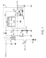
- FIG. 1 shows an exemplary embodiment of a switching power converter
- FIGS. 2A and 2B show an exemplary embodiment of a switch controller of the switching power converter in FIG. 1 ;
- FIG. 3 shows an exemplary embodiment of a sample-and-hold circuit of a linear predict circuit in FIGS. 2A and 2B ;
- FIG. 4 shows an exemplary embodiment of a voltage-to-current converter of a linear predict circuit in FIGS. 2A and 2B ;
- FIG. 5 shows an exemplary embodiment of a sample-and-hold circuit of a reset circuit in FIGS. 2A and 2B ;
- FIG. 6 shows an exemplary embodiment of the voltage-to-current converter of a reset circuit in FIGS. 2A and 2B ;
- FIG. 7 shows key wave forms of a high-side synchronous rectifier circuit of the switching power converter in FIG. 1 .
- a transformer T 1 is coupled between an unregulated input voltage V IN and an output V O of a switching power converter.
- the transformer T 1 comprises a primary winding N P and two secondary windings N S1 and N S2 .
- a power switch Q 1 is coupled to the primary winding N P at an input of the transformer T 1 to regulate the transfer of energy from the unregulated input voltage V IN to the output V O of the switching power converter.
- the power switch Q 1 is coupled to receive a switching signal V G to control switching of the power switch Q 1 .
- a resistor 25 is coupled between the power switch Q 1 and a ground of the primary side of the transformer T 1 .
- a synchronous rectifier circuit 30 is coupled between the high-side of the secondary winding N S1 of the transformer T 1 and the output V O .
- the synchronous rectifier circuit 30 is composed of a switching controller 100 which serves as a control circuit for the switching power converter.
- the switching controller 100 generates a pulse width modulation (PWM) signal V G2 which serves as a switching signal for controlling a power transistor Q 2 , wherein the power transistor Q 2 serves as a power switching device for the switching power converter.
- a diode 40 is connected to the power transistor Q 2 in parallel, wherein the diode 40 is a parasitic diode.
- the switching controller 100 includes a power terminal VDD, a linear predicting terminal LPC, a reset terminal RES, a ground terminal GND, and a control terminal GATE.
- the power terminal VDD is coupled to the secondary winding N S1 to receive a rectified power source through a diode 45 and a capacitor C 6 .
- Resistors R 1 and R 2 are coupled in series between the capacitor C 6 and a ground of a secondary side of the transformer T 1 , and a linear predict signal V LPC is generated at the joint of the resistors R 1 and R 2 .
- Resistors R 3 and R 4 are coupled in series and coupled to the power transistor Q 2 in parallel, and a resetting signal V RES is generated at the joint of the resistors R 3 and R 4 .
- the linear predicting terminal LPC is coupled to receive the linear predict signal V LPC for charging and the reset terminal RES is coupled to receive the resetting signal V RES for resetting.
- the control terminal GATE is coupled to generate the PWM signal V G2 to control the power transistor Q 2 .
- FIGS. 2A and 2B show an exemplary embodiment of the switching controller 100 .
- the switching controller 100 comprises a linear predict circuit 101 , a reset circuit 103 , a PWM circuit 107 , and a charge/discharge circuit.
- the linear predict circuit 101 is composed of a sample-and-hold circuit 102 and a voltage-to-current converter (V/I) 106 .
- the reset circuit 103 is also composed of a sample-and-hold circuit 104 and a voltage-to-current converter (V/I) 105 .
- the charge/discharge circuit comprises a capacitor C 3 and a switch SW 4 .
- the PWM circuit 107 is composed of an SR-flip-flop 112 , an inverter 113 , and comparators 108 and 110 .
- the linear predict circuit 101 is coupled to receive the linear predict signal V LPC for charging to the capacitor C 3 through a sampling-and-hold operation.
- the linear predict circuit 101 is composed of the sample and hold circuit 102 and the voltage to current converter (V/I) 106 .
- the sample-and-hold circuit 102 of the linear predict circuit 101 is coupled to receive the linear predict signal V LPC for sampling at a rising edge of the linear predict signal V LPC , and then hold a sampling signal V SL (shown in FIG. 3 ) at a falling edge of the linear predict signal V LPC to generate a hold signal V HL (shown in FIG. 3 ).
- the voltage-to-current converter (V/I) 106 is coupled to generate a charging current (also referred as a charging signal) I 3 in response the hold signal V HL .
- the reset circuit 103 is also composed of the sample-and-hold circuit 104 and the voltage-to-current converter (V/I) 105 .
- the reset circuit 103 is coupled to receive the resetting signal V RES to generate a discharge signal for resetting the PWM circuit 107 through the charge/discharge circuit.
- the sample-and-hold circuit 104 is coupled to receive the resetting signal V RES for sampling at a rising edge of the resetting signal V RES , and hold the sampling result (sampling signal V SR shown in FIG. 5 ) at a falling edge of the resetting signal V RES to generate a hold signal V HR (shown in FIG. 5 ).
- the voltage-to-current converter (V/I) 105 is coupled to generate a discharging current (also referred as a discharging signal) I DIS in response the hold signal V HR for resetting the PWM circuit 107 through the charge/discharge circuit.
- a discharging current also referred as a discharging signal
- the charge/discharge circuit comprises the capacitor C 3 and the switch SW 4 , which are coupled in series, for receiving the charging current I 3 and receiving the discharging current I DIS through the switch SW 4 .
- the capacitor C 3 is coupled to receive the charging current I 3 for charging, and the discharging current I DIS is generated from the voltage-to-current converter (V/I) 105 through the switch SW 4 while the switch SW 4 is turned on as shown in FIG. 2B .
- a ramp signal V CT is thus generated at the joint of the capacitor C 3 and the switch SW 4 in response to the charging current I 3 and the discharging current I DIS .
- the SR-flip-flop 112 , the inverter 113 , and the comparators 108 and 110 develop the PWM circuit 107 for generating the PWM signal V G2 at the output terminal Q of the SR-flip-flop 112 in response to the linear predict signal V LPC and the ramp signal V CT .
- the setting terminal S of the SR-flip-flop 112 is controlled by an output of the comparator 108 .
- the comparator 108 are coupled to receive the linear predict signal V LPC and a first threshold V TH1 for comparison.
- the resetting terminal R of the SR-flip-flop 112 is controlled by an output of the comparator 110 .
- the comparator 110 is couple to receive the ramp signal V CT and a second threshold V TH2 for comparison.
- the comparator 108 generates an enabling signal E N according to the comparison result.
- the inverter 113 is coupled to receive the enabling signal E N and generate an inverse enabling signal ENB.
- FIG. 3 shows an exemplary embodiment of the sample-and-hold circuit 102 .
- a buffer 201 , a switch 202 , and a capacitor C 1 form a sample circuit, and another switch 203 and a capacitor C 2 form a hold circuit.
- the linear predict signal V LPC is coupled to generate a first signal S 1 and a second signal S 2 to control the switch 202 and the switch 203 through pulse generation circuits 204 and 205 , respectively.
- the first signal S 1 is enabled in response to the rising edge of the linear predict signal V LPC via the pulse generation circuits 204
- the second signal S 2 is enabled in response to the falling edge of the predict signal V LPC via the pulse generation circuits 205 .
- the sampling signal V SL is generated through the switch 202 at the rising edge of the linear predict signal V LPC , and the hold signal V HL is thus generated in the capacitor C 2 at the falling edge of the linear predict signal V LPC .
- the hold signal V HL is correlated to the high level of the linear predict signal V LPC .
- FIG. 4 shows an exemplary embodiment of the voltage-to-current converter (V/I) 106 , wherein an operational amplifier 210 , a transistor 211 , and a resistor 212 develop a V-to-I circuit to generate a current I 212 in response to the hold signal V HL .
- Transistors 213 , 214 , 215 , 216 , and 217 develop current mirrors to generate currents I 214 , I 215 and I 3 in response to the current I 212 .
- the charging current I 3 is proportional to the current I 212 .
- the charging current I 3 is coupled to the capacitor C 3 for charging.
- FIG. 5 shows an exemplary embodiment of the sample-and-hold circuit 104 .
- a buffer 301 , a switch 302 , and a capacitor C 4 form a sample circuit, and another switch 303 and a capacitor C 5 form a hold circuit.
- the resetting signal V RES is coupled to generate a first signal S 3 and a second signal S 4 to control switch 302 and switch 303 through pulse generation circuits 304 and 305 , respectively.
- the first signal S 3 is enabled in response to the rising edge of the resetting signal V RES via the pulse generation circuits 304
- the second signal S 2 is enabled in response to the falling edge of the resetting signal V RES via the pulse generation circuits 305 .
- the sampling signal V SR is generated through the switch S 3 at the rising edge of the resetting signal V RES , and the hold signal V HR is thus generated in the capacitor C 5 at the falling edge of the resetting signal V RES .
- the hold signal V HR is correlated to the high level of the resetting signal V RES .
- FIG. 6 shows an exemplary embodiment of the voltage-to-current converter (V/I) 105 , wherein an operational amplifier 310 , a transistor 311 , and a resistor 312 develop a V-to-I circuit to generate a current I 311 in response to the hold signal V HR .
- Transistors 313 and 314 develop a current mirror to generate currents I 314 in response to the current I 311 .
- the current I 314 is mirrored form the current I 311 , and the current I 311 represents the resetting signal V RES
- the I 214 is mirrored form the current I 212 , and the current I 212 represents the linear predict signal V LPC . So the discharging current I DIS represents the difference between the resetting signal V RES and the linear predict signal V LPC .
- FIG. 7 shows the key wave forms of the high-side synchronous rectifier circuit.
- the switching signal V G is enabled, the diode 45 and diode 40 are turned off (reversed biased).
- the voltage of the linear predict signal V LPC is in a high level, which can be express as
- V LPC V i ⁇ ⁇ n n ⁇ R 2 R 1 + R 2
- the PWM signal V G2 is disabled in response to the high level of the linear predict signal V LPC at the mean time.
- the power transistor Q 2 is switched off. While the switching signal V G is disabled, the diode 45 and diode 40 are turned on (forward biased).
- the PWM signal V G2 is enabled in response to the low level of the linear predict signal V LPC .
- the ramp signal V CT is discharged in response to the difference between the resetting signal V RES and the linear predict signal V LPC .
- the PWM signal V G2 is disabled once the voltage of the ramp signal V CT is lower then the second threshold V TH2 .
- the switching controller can be installed at high-side of secondary side of a switching power converter. Therefore, the ground terminal of the switching controller is no more coupled to a ground of low-side of a secondary side of a power converter but coupled to a relative low voltage of the high side winding. So the switching loss and electric-magnetic-interference (EMI) problem caused by the switching operation of the ground of the secondary side of the switching power converter can be solved.
- EMI electric-magnetic-interference
Landscapes
- Engineering & Computer Science (AREA)
- Power Engineering (AREA)
- Dc-Dc Converters (AREA)
Abstract
Description
and the PWM signal VG2 is disabled in response to the high level of the linear predict signal VLPC at the mean time. The power transistor Q2 is switched off. While the switching signal VG is disabled, the
Claims (8)
Priority Applications (1)
| Application Number | Priority Date | Filing Date | Title |
|---|---|---|---|
| US13/112,414 US8625313B2 (en) | 2010-08-04 | 2011-05-20 | High-side synchronous rectifier circuits and control circuits for power converters |
Applications Claiming Priority (2)
| Application Number | Priority Date | Filing Date | Title |
|---|---|---|---|
| US37047810P | 2010-08-04 | 2010-08-04 | |
| US13/112,414 US8625313B2 (en) | 2010-08-04 | 2011-05-20 | High-side synchronous rectifier circuits and control circuits for power converters |
Publications (2)
| Publication Number | Publication Date |
|---|---|
| US20120033460A1 US20120033460A1 (en) | 2012-02-09 |
| US8625313B2 true US8625313B2 (en) | 2014-01-07 |
Family
ID=45337159
Family Applications (1)
| Application Number | Title | Priority Date | Filing Date |
|---|---|---|---|
| US13/112,414 Active 2032-04-12 US8625313B2 (en) | 2010-08-04 | 2011-05-20 | High-side synchronous rectifier circuits and control circuits for power converters |
Country Status (3)
| Country | Link |
|---|---|
| US (1) | US8625313B2 (en) |
| CN (1) | CN102290996B (en) |
| TW (1) | TWI436571B (en) |
Cited By (4)
| Publication number | Priority date | Publication date | Assignee | Title |
|---|---|---|---|---|
| TWI514741B (en) * | 2014-01-27 | 2015-12-21 | Leadtrend Tech Corp | Synchronous rectification control method and synchronous rectification controller capable of providing a programmable dead time |
| US10075084B2 (en) * | 2016-12-16 | 2018-09-11 | Rohm Co., Ltd. | Isolated synchronous rectification-type DC/DC converter |
| US20190222134A1 (en) * | 2018-01-17 | 2019-07-18 | Rohm Co., Ltd. | Isolated synchronous rectifying dc/dc converter |
| US20210075319A1 (en) * | 2015-05-15 | 2021-03-11 | On-Bright Electronics (Shanghai) Co., Ltd. | Systems and methods for output current regulation in power conversion systems |
Families Citing this family (21)
| Publication number | Priority date | Publication date | Assignee | Title |
|---|---|---|---|---|
| US10622902B2 (en) | 2012-04-12 | 2020-04-14 | On-Bright Electronics (Shanghai) Co., Ltd. | Systems and methods for regulating power conversion systems with output detection and synchronized rectifying mechanisms |
| US9595874B2 (en) | 2012-04-12 | 2017-03-14 | On-Bright Electronics (Shanghai) Co., Ltd. | Systems and methods for regulating power conversion systems with output detection and synchronized rectifying mechanisms |
| US9413246B2 (en) | 2012-04-12 | 2016-08-09 | On-Bright Electronics (Shanghai) Co., Ltd. | Systems and methods for regulating power conversion systems with output detection and synchronized rectifying mechanisms |
| CN103378751B (en) | 2012-04-12 | 2015-04-01 | 昂宝电子(上海)有限公司 | System and method used for flyback switch power source transformation system |
| TWI496406B (en) * | 2012-07-03 | 2015-08-11 | System General Corp | Power converter and method for controlling power converter |
| TWI462445B (en) * | 2012-10-19 | 2014-11-21 | Lite On Technology Corp | Power converting device |
| TWI451675B (en) * | 2012-10-31 | 2014-09-01 | Lite On Technology Corp | Synchronously regulating controller circuit and power converting device |
| US9369054B2 (en) * | 2013-11-01 | 2016-06-14 | Dialog Semiconductor Inc. | Reducing power consumption of a synchronous rectifier controller |
| TWI555320B (en) * | 2014-01-27 | 2016-10-21 | 葉文中 | Method for providing switch-timing, synchronous rectifier controller, and adaptive timing controller |
| CN104901564B (en) * | 2014-03-07 | 2017-09-26 | 通嘉科技股份有限公司 | Switch timing sequence providing method, synchronous rectification controller and adaptive timing controller |
| CN104932602B (en) * | 2014-03-19 | 2017-04-12 | 力智电子股份有限公司 | Integrated circuit with multi-function parameter setting and its multi-function parameter setting method |
| US9812978B2 (en) * | 2015-04-02 | 2017-11-07 | Virginia Tech Intellectual Properties, Inc. | Circuit and method for driving synchronous rectifiers for high-frequency flyback converters |
| CN105305844B (en) * | 2015-10-21 | 2017-11-21 | 深圳市芯茂微电子有限公司 | A kind of isolated form synchronous commutating control circuit and its device and control method |
| CN106026703B (en) * | 2016-05-23 | 2018-07-13 | 昂宝电子(上海)有限公司 | System and method with the forecasting mechanism for synchronous rectifying controller |
| CN106817031B (en) | 2017-02-24 | 2019-05-28 | 昂宝电子(上海)有限公司 | With the time-controlled system and method for synchronous rectifying controller |
| JP7307599B2 (en) * | 2019-06-18 | 2023-07-12 | ローム株式会社 | Synchronous controller and isolated synchronous DC/DC converter |
| CN110855131B (en) * | 2019-12-09 | 2021-10-15 | 成都芯源系统有限公司 | Drive circuit of synchronous rectifier |
| CN111146961B (en) | 2020-01-20 | 2022-04-12 | 昂宝电子(上海)有限公司 | Control circuit and method for controlling synchronous rectification system |
| CN111697838B (en) | 2020-05-29 | 2023-09-26 | 昂宝电子(上海)有限公司 | Synchronous rectification control circuit, method and switching power supply system |
| CN112821727B (en) | 2021-03-11 | 2022-06-28 | 昂宝电子(上海)有限公司 | Switching power supply system |
| CN113472211B (en) | 2021-07-07 | 2022-12-23 | 昂宝电子(上海)有限公司 | Flyback switching power supply and synchronous rectification controller thereof |
Citations (2)
| Publication number | Priority date | Publication date | Assignee | Title |
|---|---|---|---|---|
| US7206208B1 (en) * | 2006-01-13 | 2007-04-17 | Niko Semiconductor Co., Ltd. | Synchronous rectifying control circuit |
| US7440298B2 (en) * | 2006-08-11 | 2008-10-21 | System General Corp. | Synchronous rectification circuit for power converters |
Family Cites Families (1)
| Publication number | Priority date | Publication date | Assignee | Title |
|---|---|---|---|---|
| CN101047338A (en) * | 2007-04-29 | 2007-10-03 | 艾默生网络能源有限公司 | Synchronous rectificiation circuit of DC/DC inverter |
-
2011
- 2011-05-20 US US13/112,414 patent/US8625313B2/en active Active
- 2011-07-11 TW TW100124406A patent/TWI436571B/en active
- 2011-07-18 CN CN201110200544.9A patent/CN102290996B/en active Active
Patent Citations (2)
| Publication number | Priority date | Publication date | Assignee | Title |
|---|---|---|---|---|
| US7206208B1 (en) * | 2006-01-13 | 2007-04-17 | Niko Semiconductor Co., Ltd. | Synchronous rectifying control circuit |
| US7440298B2 (en) * | 2006-08-11 | 2008-10-21 | System General Corp. | Synchronous rectification circuit for power converters |
Cited By (7)
| Publication number | Priority date | Publication date | Assignee | Title |
|---|---|---|---|---|
| TWI514741B (en) * | 2014-01-27 | 2015-12-21 | Leadtrend Tech Corp | Synchronous rectification control method and synchronous rectification controller capable of providing a programmable dead time |
| US20210075319A1 (en) * | 2015-05-15 | 2021-03-11 | On-Bright Electronics (Shanghai) Co., Ltd. | Systems and methods for output current regulation in power conversion systems |
| US11652410B2 (en) * | 2015-05-15 | 2023-05-16 | On-Bright Electronics (Shanghai) Co., Ltd. | Systems and methods for output current regulation in power conversion systems |
| US10075084B2 (en) * | 2016-12-16 | 2018-09-11 | Rohm Co., Ltd. | Isolated synchronous rectification-type DC/DC converter |
| US10483863B2 (en) | 2016-12-16 | 2019-11-19 | Rohm Co., Ltd. | Isolated synchronous rectification-type DC/DC converter |
| US20190222134A1 (en) * | 2018-01-17 | 2019-07-18 | Rohm Co., Ltd. | Isolated synchronous rectifying dc/dc converter |
| US10566910B2 (en) * | 2018-01-17 | 2020-02-18 | Rohm Co., Ltd. | Isolated synchronous rectifying DC/DC converter |
Also Published As
| Publication number | Publication date |
|---|---|
| CN102290996A (en) | 2011-12-21 |
| TW201220664A (en) | 2012-05-16 |
| TWI436571B (en) | 2014-05-01 |
| CN102290996B (en) | 2014-05-28 |
| US20120033460A1 (en) | 2012-02-09 |
Similar Documents
| Publication | Publication Date | Title |
|---|---|---|
| US8625313B2 (en) | High-side synchronous rectifier circuits and control circuits for power converters | |
| US9812856B2 (en) | Modulation mode control circuit, switch control circuit including the modulation mode control circuit and power supply device including the switch control circuit | |
| US10128762B2 (en) | Semiconductor device for controlling power source | |
| US8045351B2 (en) | Method and apparatus of providing a biased current limit for limiting maximum output power of power converters | |
| CN111756247B (en) | Switching power supply device | |
| US8023291B2 (en) | Voltage detecting circuit and switching power source apparatus | |
| US10044276B2 (en) | Phase-cut pre-regulator and power supply comprising the same | |
| US20120201055A1 (en) | Power supply and apparatus and method for controlling link voltage control switch | |
| US8576595B2 (en) | Method and apparatus of providing a biased current limit for limiting maximum output power of power converters | |
| US8115466B2 (en) | Converter and driving method thereof | |
| JP2009284667A (en) | Power supply device, its control method, and semiconductor device | |
| JP2020162326A (en) | Switching power supply device | |
| US20100302824A1 (en) | Power source apparatus | |
| US11703550B2 (en) | Resonance voltage attenuation detection circuit, semiconductor device for switching power, and switching power supply | |
| US20110254537A1 (en) | Method and Apparatus for Detecting CCM Operation of a Magnetic Device | |
| US10381941B2 (en) | Switching power supply device and synchronous rectifier circuit | |
| JP2015186363A (en) | DC-DC converter | |
| US8139381B2 (en) | Power converter, and switching controller and driving method thereof | |
| JP2017204921A (en) | Switching power supply | |
| JPH1155944A (en) | Switching power supply equipment | |
| US9379622B2 (en) | Power converter and method for controlling power converter | |
| JP7602389B2 (en) | Power supply control device and flyback converter | |
| EP3070828A1 (en) | Power apparatus | |
| JP6487874B2 (en) | Switching power supply | |
| US20250030348A1 (en) | Semiconductor device for switching power supply and switching power supply device |
Legal Events
| Date | Code | Title | Description |
|---|---|---|---|
| AS | Assignment |
Owner name: SYSTEM GENERAL CORPORATION, TAIWAN Free format text: ASSIGNMENT OF ASSIGNORS INTEREST;ASSIGNORS:YEH, CHIA-YO;HSU, JHIH-DA;SU, YING-CHIEH;AND OTHERS;REEL/FRAME:026315/0900 Effective date: 20110518 |
|
| STCF | Information on status: patent grant |
Free format text: PATENTED CASE |
|
| AS | Assignment |
Owner name: FAIRCHILD (TAIWAN) CORPORATION, TAIWAN Free format text: CHANGE OF NAME;ASSIGNOR:SYSTEM GENERAL CORPORATION;REEL/FRAME:038599/0043 Effective date: 20140620 |
|
| AS | Assignment |
Owner name: SEMICONDUCTOR COMPONENTS INDUSTRIES, LLC, ARIZONA Free format text: ASSIGNMENT OF ASSIGNORS INTEREST;ASSIGNOR:FAIRCHILD (TAIWAN) CORPORATION (FORMERLY SYSTEM GENERAL CORPORATION);REEL/FRAME:042328/0318 Effective date: 20161221 |
|
| FPAY | Fee payment |
Year of fee payment: 4 |
|
| AS | Assignment |
Owner name: DEUTSCHE BANK AG NEW YORK BRANCH, AS COLLATERAL AGENT, NEW YORK Free format text: PATENT SECURITY AGREEMENT;ASSIGNOR:SEMICONDUCTOR COMPONENTS INDUSTRIES, LLC;REEL/FRAME:046410/0933 Effective date: 20170210 Owner name: DEUTSCHE BANK AG NEW YORK BRANCH, AS COLLATERAL AG Free format text: PATENT SECURITY AGREEMENT;ASSIGNOR:SEMICONDUCTOR COMPONENTS INDUSTRIES, LLC;REEL/FRAME:046410/0933 Effective date: 20170210 |
|
| MAFP | Maintenance fee payment |
Free format text: PAYMENT OF MAINTENANCE FEE, 8TH YEAR, LARGE ENTITY (ORIGINAL EVENT CODE: M1552); ENTITY STATUS OF PATENT OWNER: LARGE ENTITY Year of fee payment: 8 |
|
| AS | Assignment |
Owner name: FAIRCHILD SEMICONDUCTOR CORPORATION, ARIZONA Free format text: RELEASE OF SECURITY INTEREST IN PATENTS RECORDED AT RECORDED AT REEL 046410, FRAME 0933;ASSIGNOR:DEUTSCHE BANK AG NEW YORK BRANCH, AS COLLATERAL AGENT;REEL/FRAME:064072/0001 Effective date: 20230622 Owner name: SEMICONDUCTOR COMPONENTS INDUSTRIES, LLC, ARIZONA Free format text: RELEASE OF SECURITY INTEREST IN PATENTS RECORDED AT RECORDED AT REEL 046410, FRAME 0933;ASSIGNOR:DEUTSCHE BANK AG NEW YORK BRANCH, AS COLLATERAL AGENT;REEL/FRAME:064072/0001 Effective date: 20230622 |