US8618674B2 - Semiconductor device including a sintered insulation material - Google Patents
Semiconductor device including a sintered insulation material Download PDFInfo
- Publication number
- US8618674B2 US8618674B2 US12/237,968 US23796808A US8618674B2 US 8618674 B2 US8618674 B2 US 8618674B2 US 23796808 A US23796808 A US 23796808A US 8618674 B2 US8618674 B2 US 8618674B2
- Authority
- US
- United States
- Prior art keywords
- chip
- sintered
- semiconductor device
- carrier
- insulation material
- Prior art date
- Legal status (The legal status is an assumption and is not a legal conclusion. Google has not performed a legal analysis and makes no representation as to the accuracy of the status listed.)
- Expired - Fee Related, expires
Links
Images


Classifications
-
- H10W74/114—
-
- H10W70/093—
-
- H10W70/611—
-
- H10W70/614—
-
- H10W70/635—
-
- H10W74/141—
-
- H10W90/00—
-
- H10W70/05—
-
- H10W70/479—
-
- H10W70/60—
-
- H10W72/874—
-
- H10W72/926—
-
- H10W72/9413—
-
- H10W74/00—
-
- H10W90/734—
-
- H10W90/736—
Definitions
- Some electronic devices such as cellular telephones, employ a variety of design-specific electronic components.
- Other electronic devices such as power packages utilized in the automotive industry, employ one or more logic chips connected to a leadframe and one or more power transistors connected to the leadframe and the logic chip(s).
- the space available inside the electronic devices is limited, particularly as the electronic devices are made smaller.
- Dielectric or insulating materials having good thermal and mechanical characteristics are typically used within the electronic devices.
- the dielectric or insulating materials are typically structured using an encapsulation procedure due to the high processing temperatures and/or processing pressures for the materials.
- the insulating or dielectric structures are planar or surface-conformal, which may provide inadequate isolation at some points within the electronic devices, such as at chip edges.
- the semiconductor device includes a carrier and a first chip attached to the carrier.
- the semiconductor device includes a sintered insulation material over at least a portion of the carrier and the first chip.
- FIG. 1 illustrates a cross-sectional view of one embodiment of a semiconductor device.
- FIG. 2 illustrates a top view of one embodiment of a semiconductor device.
- FIG. 3 illustrates a cross-sectional view of one embodiment of a portion of the semiconductor device illustrated in FIG. 2 .
- FIG. 4 illustrates a cross-sectional view of one embodiment of a carrier, a logic chip, and a power transistor.
- FIG. 5 illustrates a cross-sectional view of one embodiment of the carrier, the logic chip, the power transistor, and a dielectric material powder.
- FIG. 6 illustrates a cross-sectional view of one embodiment of the carrier, the logic chip, the power transistor, and the dielectric material powder during sintering of the dielectric material powder.
- FIG. 7 illustrates a cross-sectional view of one embodiment of the carrier, the logic chip, the power transistor, and sintered dielectric material after removing the unsintered dielectric material powder.
- FIG. 8 illustrates a cross-sectional view of one embodiment of the carrier, the logic chip, the power transistor, the sintered dielectric material, and a metal powder.
- FIG. 9 illustrates a cross-sectional view of one embodiment of the carrier, the logic chip, the power transistor, the sintered dielectric material, and the metal powder during sintering of the metal powder.
- FIG. 10 illustrates a cross-sectional view of one embodiment of the carrier, the logic chip, the power transistor, the sintered dielectric material, and conducting elements after removing the unsintered metal powder.
- FIG. 11 illustrates a cross-sectional view of another embodiment of a semiconductor device.
- FIG. 12 illustrates a cross-sectional view of one embodiment of a carrier, a chip, and first dielectric material powder.
- FIG. 13 illustrates a cross-sectional view of one embodiment of the carrier, the chip, and first sintered dielectric material after sintering portions of the first dielectric material powder and removing the unsintered first dielectric material powder.
- FIG. 14 illustrates a cross-sectional view of one embodiment of the carrier, the chip, the first sintered dielectric material, and second dielectric material powder.
- FIG. 15 illustrates a cross-sectional view of one embodiment of the carrier, the chip, the first sintered dielectric material, and second sintered dielectric material after sintering portions of the second dielectric material powder and removing the unsintered second dielectric material powder.
- FIG. 16 illustrates a cross-sectional view of one embodiment of the carrier, the chip, the first sintered dielectric material, the second sintered dielectric material, and conducting elements.
- FIG. 17A illustrates a cross-sectional view of one embodiment of a via.
- FIG. 17B illustrates a cross-sectional view of another embodiment of a via.
- FIG. 17C illustrates a cross-sectional view of another embodiment of a via.
- FIG. 18A illustrates a cross-sectional view of one embodiment of an opening for adhesion to a mold compound.
- FIG. 18B illustrates a cross-sectional view of another embodiment of an opening for adhesion to a mold compound.
- FIG. 18C illustrates a cross-sectional view of another embodiment of an opening for adhesion to a mold compound.
- FIG. 1 illustrates a cross-sectional view of one embodiment of a semiconductor device 90 .
- Semiconductor device 90 includes a carrier 92 , a chip 94 , and sintered dielectric or insulation material 96 .
- Chip 94 is attached to carrier 92 .
- Sintered insulation material 96 is over at least a portion of carrier 92 and chip 94 .
- a dielectric material powder is applied over carrier 92 and chip 94 .
- a laser beam is then applied to portions of the dielectric material powder where insulation material is desired to be structured.
- the laser beam sinters the portions of the dielectric material powder to provide a sintered insulation material.
- the remaining unsintered dielectric material powder is then removed.
- the process of applying the dielectric material powder, sintering portions of the dielectric material powder, and removing the unsintered dielectric material powder can be repeated any suitable number of times to form any suitable insulating structure having a desired configuration.
- FIG. 2 illustrates a top view of one embodiment of a semiconductor device 100 .
- semiconductor device 100 is a semiconductor device power package.
- Semiconductor device 100 includes a sintered dielectric or insulating structure.
- Semiconductor device 100 includes a carrier 102 , chips 104 , 106 , 108 , and 110 coupled to carrier 102 , a conducting element 112 extending between chip 104 and carrier 102 , a conducting element 114 extending between chip 106 and chip 108 , a conducting element 116 extending between chip 106 and chip 110 , and a conducting element 118 extending between chip 110 and carrier 102 .
- Semiconductor device 100 also includes other suitable electrical connections between chips 104 , 106 , 108 , 110 , and carrier 102 .
- carrier 102 includes a leadframe having a plurality of connection heads or contact pads 120 , one or more islands 122 , and one or more connection strips 124 .
- carrier 102 includes a leadframe stamped from a plate of copper or another suitable conductor to include contact pads 120 , islands 122 , and connection strip 124 . The components of carrier 102 are retained in a desired orientation until chips 104 , 106 , 108 , and 110 are attached to islands 122 and appropriately electrically connected.
- carrier 102 provides a support structure for semiconductor device 100 and includes a leadframe formed of metal such as copper, aluminum, an alloy of copper, an alloy of aluminum, or other suitable electrically conducting metal.
- carrier 102 includes a quad flat no-lead (QFN) frame having contacts pads 120 on more than two sides. In another embodiment, carrier 102 includes a dual flat no-lead (DFN) frame having contact pads 120 on two opposing sides. In other embodiments, other suitable carriers are used.
- QFN quad flat no-lead
- DFN dual flat no-lead
- chips 104 and 106 are logic chips and chips 108 and 110 are power transistors.
- Power transistors 108 and 110 include wider conducting elements 118 electrically coupled to carrier 102 that are configured to bring power from the outside world to drive chips 104 and 106 .
- chip 104 is a controller chip and chip 106 is a driver chip, where chips 104 and 106 provide logic and processing for semiconductor device 100 .
- other suitable forms and styles of chips 104 , 106 , 108 , and 110 are used.
- Conducting elements 112 , 114 , 116 , and 118 electrically connect components disposed on carrier 102 to the outside world.
- conducting elements 112 , 114 , 116 , and 118 are sintered metallic lines accurately traced onto carrier 102 and coupled to chips 104 , 106 , 108 , and 110 in a direct process.
- Conducting elements 112 and 114 are generally electrically conducting element having a line width of between about 1-20 micrometers and couple between one or more chips 104 , 106 , 108 , and 110 or between chips 104 , 106 , 108 , and 110 and one or more pads 120 of carrier 102 .
- Conducting element 118 is fabricated to be wider than conducting elements 112 and 114 .
- conducting element 118 is a high voltage sintered line having a width of between about 15-50 micrometers and is electrically coupled between power transistors 108 and 110 and carrier 102 .
- FIG. 3 illustrates a cross-sectional view of one embodiment of a portion 140 of semiconductor device 100 taken along line 2 - 2 of FIG. 2 .
- the cross-section represents a semiconductor device 140 including logic chip 106 and power transistor 108 attached to carrier 102 and including conducting elements 114 electrically coupling logic chip 106 , power transistor 108 , and carrier 102 .
- logic chip 106 is attached to carrier 102 by an adhesive 142 or another suitable attachment material.
- Power transistor 108 is likewise attached to carrier 102 .
- power transistor 108 is adhesively attached to carrier 102 .
- power transistor 108 is vertically integrated into carrier 102 .
- a sintered dielectric material 144 is formed around and over portions of logic chip 106 , power transistor 108 , and carrier 102 . Sintered dielectric material 144 electrically insulates portions of logic chip 106 , power transistor 108 , and carrier 102 .
- Embodiments provided herein and described below include the sintered dielectric material 144 and sintered conducting elements 114 electrically connected to logic chip 106 and power transistor 108 and extending over portions of sintered dielectric material 144 .
- a conducting element 114 defines an uppermost contact surface 146 of logic chip 106 and the conducting element 114 is sintered between logic chip 106 and uppermost contact surface 146 . In other words, an entire depth of the conducting element 114 is sintered between logic chip 106 and uppermost contact surface 146 .
- a conducting element 114 is sintered between power transistor 108 and an uppermost surface 148 of power transistor 108 .
- FIGS. 4-10 illustrates embodiments of a method for fabricating semiconductor device 140 previously described and illustrated with reference to FIG. 3 .
- FIG. 4 illustrates a cross-sectional view of one embodiment of a carrier 102 , a logic chip 106 , and a power transistor 108 .
- Logic chip 106 is attached to carrier 102 using adhesive 142 or another suitable attachment material.
- Power transistor 108 is likewise attached to carrier 102 .
- power transistor 108 is adhesively attached to carrier 102 .
- power transistor 108 is vertically integrated into carrier 102 .
- FIG. 5 illustrates a cross-sectional view of one embodiment of carrier 102 , logic chip 106 , power transistor 108 , and dielectric material powder 150 .
- Dielectric material powder 150 include particles of a polyimide, a polyisocyanate, a polyurethane, a liquid-crystalline polymer, a high-temperature-resistant thermoplastic, a duroplast, a silicone, a copolymer, a phenol resin, an amino resin, a siloxane, an unsaturated polyester, a polybenzoxazole, a polybenzimidazole, an epoxide, a ceramic, TiO 2 , ZrO 2 , Al 2 O 3 , SiO 2 , or other suitable dielectric material powder.
- dielectric material powder 150 is selected to have a particle size of between about 2 nanometers (nm) to 10 micrometers ( ⁇ m), and preferably the particle size is between about 5 nm to 1 ⁇ m.
- the dielectric material powder is applied electrostatically or by using another suitable technique.
- FIG. 6 illustrates a cross-sectional view of one embodiment of carrier 102 , logic chip 106 , power transistor 108 , and dielectric material powder 150 during sintering of the dielectric material powder.
- Dielectric material powder 150 is sintered to provide sintered dielectric material 144 .
- Dielectric material powder 150 is sintered by a laser 152 .
- Laser 152 is directed in a path to the right for example, as indicated by arrows 156 .
- Laser 152 provides a beam 154 that moves along the surface of carrier 102 , logic chip 106 , and power transistor 108 and sinters the dielectric material powder 150 in contact with beam 154 .
- the particles in dielectric material powder 150 that are energetically affected by beam 154 are sintered to form sintered dielectric material 144 .
- laser 152 includes a neodymium-doped yttrium aluminum garnet (Nd:YAG) solid state laser, a CO 2 or gas laser, a diode laser, or other suitable electron beam high energy source.
- the Nd:YAG laser has a power between 100-2000 watts operating at a speed between 40-80 mm/s. In other embodiments, other suitable lasers operated at other powers and transport speeds are used.
- the Nd:YAG laser emits light at a wave length of about 1064 nanometers in the infrared spectrum, although transitions near the 940 , 1120 , 1320 , and 1440 nanometer range are present.
- Suitable lasers may be operated in both pulsed and/or continuous mode.
- One suitable Nd:YAG laser is available from Han's Laser Technology Company, Houston, Tex.
- FIG. 7 illustrates a cross-sectional view of one embodiment of carrier 102 , logic chip 106 , power transistor 108 , and sintered dielectric material 144 after removing unsintered dielectric material powder 150 .
- the dielectric material powder 150 that is not sintered by laser 152 is removed from logic chip 106 , power transistor 108 , and carrier 102 by a suitable removal process, such as washing, air pistol, etc. to expose portions of logic chip 106 , power transistor 108 , and carrier 102 .
- FIG. 8 illustrates a cross-sectional view of one embodiment of carrier 102 , logic chip 106 , power transistor 108 , sintered dielectric material 144 , and a metal powder 160 .
- Metal powder 160 includes silver powder, gold powder, nickel powder, copper powder, or other suitable electrically conducting metals provided in a powdered form.
- metal powder 160 is silver powder that is evenly distributed over an upper surface of carrier 102 , logic chip 106 , power transistor 108 , and sintered dielectric material 144 .
- Silver has a low susceptibility to oxidation.
- Silver powder is suited for distribution over the upper surfaces of logic chip 106 , power transistor 108 , and carrier 102 without special consideration for the local atmosphere.
- copper powder is evenly distributed over components placed on carrier 102 and is preferably deposited in an inert atmosphere such as a nitrogen atmosphere.
- Metal powder 160 is selected to have a particle size of between about 2 nm to 10 ⁇ m, and preferably the particle size is between about 5 nm to 1 ⁇ m.
- metal powder 160 includes silver particles having an average particle size of about 5 nm that are subsequently sintered by a high energy process to provide a conducting line having a width between about 20-50 ⁇ m and a thickness between about 1-5 ⁇ m. It has been discovered that particle sizes of less than 50 nm reduce the sintering temperature significantly, and that particle sizes of about 5 nm reduce the sintering temperature to less than about one third of the melting point for the alloy in a manner that sintering is done without pressure. It is desired that the porosity of the metal powder 160 be minimized, which results in the thermal and electrical performance being maximized.
- FIG. 9 illustrates a cross-sectional view of one embodiment of the carrier 102 , logic chip 106 , power transistor 108 , sintered dielectric material 144 , and metal powder 160 during sintering of the metal powder.
- Laser 152 is directed in a path to the right for example, as indicated by arrows 156 .
- Laser beam 154 moves along the surface of carrier 102 , logic chip 106 , and power transistor 108 and sinters the metal powder 160 in contact with beam 154 .
- the particles in metal powder 160 that are energetically affected by beam 154 are sintered to form conducting elements 114 .
- FIG. 10 illustrates a cross-sectional view of one embodiment of carrier 102 , logic chip 106 , power transistor 108 , sintered dielectric material 144 , and conducting elements 114 after removing unsintered metal powder 160 .
- the particles of metal powder 160 that are not sintered by laser 152 are removed from logic chip 106 , power transistor 108 , and carrier 102 by a suitable removal process, such as washing, air pistol, etc. to provide conducting elements 114 .
- a conducting element 114 electrically connects logic chip 106 to power transistor 108 and extends over a portion of a non-planar sintered dielectric material 144 .
- conducting element 114 is configured to be relatively thin compared to the thickness of logic chip 106 and power transistor 108 .
- conducting element 114 conforms to (i.e., is conformally deposited over) sintered dielectric material 144 in a one-pass process.
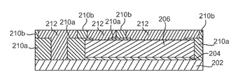
- FIG. 11 illustrates a cross-sectional view of another embodiment of a semiconductor device 200 .
- Semiconductor device 200 includes a carrier 102 , a chip 206 , sintered dielectric material 210 , and conducting elements 212 .
- Chip 206 is attached to carrier 202 by an adhesive material 204 or another suitable attachment material.
- Sintered dielectric material 210 insulates portions of chip 206 and carrier 202 .
- Sintered dielectric material 210 defines vias to carrier 202 and contacts to chip 206 in which conducting elements 212 are formed.
- conducting elements 212 include sintered metal powder.
- FIGS. 12-16 illustrate embodiments of a method for fabricating semiconductor device 200 previously described and illustrated with reference to FIG. 11 .
- FIG. 12 illustrates a cross-sectional view of one embodiment of carrier 202 , chip 206 , and first dielectric material powder 208 a .
- Chip 206 is attached to carrier 202 by an adhesive material 204 or another suitable attachment material.
- First dielectric material powder 208 a is then distributed over carrier 202 and chip 206 .
- First dielectric material powder 208 a is similar to dielectric material powder 150 previously described and illustrated with reference to FIG. 5 .
- FIG. 13 illustrates a cross-sectional view of one embodiment of carrier 202 , chip 206 , and first sintered dielectric material 210 a after sintering portions of first dielectric material powder 208 a and removing the unsintered first dielectric material powder.
- First dielectric material powder 208 a is sintered using a laser beam as previously described and illustrated with reference to FIG. 6 to provide sintered dielectric material 210 a .
- the unsintered dielectric material powder 208 a is then removed to expose portions of carrier 202 and chip 206 .
- the unsintered dielectric material powder 208 a is removed from chip 206 and carrier 202 by a suitable removal process, such as washing, air pistol, etc.
- FIG. 14 illustrates a cross-sectional view of one embodiment of carrier 202 , chip 206 , first sintered dielectric material 210 a , and second dielectric material powder 208 b .
- Second dielectric material powder 208 b is distributed over first sintered dielectric material 210 a , carrier 202 , and chip 206 .
- Second dielectric material powder 208 b is similar to dielectric material powder 150 previously described and illustrated with reference to FIG. 5 .
- FIG. 15 illustrates a cross-sectional view of one embodiment of carrier 202 , chip 206 , first sintered dielectric material 210 a , and second sintered dielectric material 210 b after sintering portions of second dielectric material powder 208 b and removing the unsintered second dielectric material powder.
- Second dielectric material powder 208 b is sintered using a laser beam as previously described and illustrated with reference to FIG. 6 to provide sintered dielectric material 210 b .
- the unsintered dielectric material powder 208 b is then removed to expose portions of first sintered dielectric material 210 a , carrier 202 , and chip 206 .
- the unsintered dielectric material powder 208 b is removed from first sintered dielectric material 210 a , chip 206 , and carrier 202 by a suitable removal process, such as washing, air pistol, etc.
- a suitable removal process such as washing, air pistol, etc.
- sintered dielectric material layer 210 b is structured upon sintered dielectric material layer 210 a to provide insulating material having a desired structure.
- sintered dielectric material layers 210 a and 210 b are structured to provide openings or vias having more than one cross-sectional width.
- opening or via 214 is defined by first sintered dielectric material 210 a and second sintered dielectric material 210 b .
- Opening 214 has a first cross-sectional width as indicated at 216 defined by first sintered dielectric material 210 a .
- Opening 214 has a second cross-sectional width as indicated at 218 defined by second sintered dielectric material 210 b .
- the second cross-sectional width indicated at 218 is greater than the first cross-sectional width indicated at 216 .
- the process of applying the dielectric material powder, sintering a portion of the dielectric material powder, and removing the unsintered dielectric material powder can be repeated any suitable number of times to provide any suitable insulating structure.
- the unsintered dielectric material powder that is removed is reused in a following application of the dielectric material powder.
- FIG. 16 illustrates a cross-sectional view of one embodiment of carrier 202 , chip 206 , first sintered dielectric material 210 a , second sintered dielectric material 210 b , and conducting elements 212 .
- Conducting elements 212 are formed in the vias or openings defined by first sintered dielectric material 210 a and second sintered dielectric material 210 b .
- conducting elements 212 are provided by applying a metal powder and sintering the metal powder as previously described and illustrated with reference to FIGS. 8-10 .
- metal is deposited over carrier 202 , sintered dielectric material 210 a and 210 b , and chip 206 and then planarized and/or etched to expose second sintered dielectric material 210 b to provide conducting elements 212 .
- FIGS. 17A-17C each illustrate a cross-sectional view of one embodiment of a via 220 a , a via 220 b , and a via 220 c , respectively.
- Vias 220 a , 220 b , and 220 c are defined by sintered dielectric material 210 .
- vias 220 a , 220 b , and/or 220 c are used in semiconductor device 200 previously described and illustrated with reference to FIG. 11 .
- Vias 220 a , 220 b , and 220 c are structured by repeating, a suitable number of times, the process of applying dielectric material powder, sintering a portion of the dielectric material powder, and removing the unsintered dielectric material powder to provide vias 220 a , 220 b , and 220 c having a desired structure.
- Via 220 a has a bottle-like shape having a plurality of cross-sectional widths.
- Via 220 b has a cross-like shape having a plurality of cross-sectional widths.
- Via 220 c has an upside down bottle-like shape having a plurality of cross-sectional widths.
- vias having other suitable three dimensional shapes are defined by sintered dielectric material 210 such that the vias have at least two cross-sectional widths.
- FIGS. 18A-18C each illustrate a cross-sectional view of one embodiment of an opening 230 a , an opening 230 b , and an opening 230 c , respectively, for adhesion to a mold compound. Openings 230 a , 230 b , and 230 c are defined by sintered dielectric material 210 . In one embodiment, opening 230 a , 230 b , and/or 230 c are used in semiconductor device 200 previously described and illustrated with reference to FIG. 11 .
- Openings 230 a , 230 b , and 230 c are structured by repeating, a suitable number of times, the process of applying dielectric material powder, sintering a portion of the dielectric material powder, and removing the unsintered dielectric material powder to provide openings 230 a , 230 b , and 230 c having a desired structure.
- Opening 230 a has a triangle-like shape having a plurality of cross-sectional widths.
- Opening 230 b has an oblong-like shape having a plurality of cross-sectional widths.
- Opening 230 c has a multiple finger-like shape having a plurality of cross-sectional widths.
- openings having other suitable three dimensional shapes are defined by sintered dielectric material 210 such that the openings have at least two cross-sectional widths.
- Embodiments provide semiconductor devices, such as semiconductor power device packages, including structured dielectric material.
- the dielectric material is structured by selectively sintering dielectric material powder using a laser beam.
- the unsintered dielectric material powder is removed for reuse.
- the process of applying the dielectric material powder, sintering portions of the dielectric material powder, and removing the unsintered dielectric material powder is repeated any suitable number of times to provide any suitable insulating material structure.
Landscapes
- Structures Or Materials For Encapsulating Or Coating Semiconductor Devices Or Solid State Devices (AREA)
- Die Bonding (AREA)
- Wire Bonding (AREA)
Abstract
Description
Claims (24)
Priority Applications (2)
| Application Number | Priority Date | Filing Date | Title |
|---|---|---|---|
| US12/237,968 US8618674B2 (en) | 2008-09-25 | 2008-09-25 | Semiconductor device including a sintered insulation material |
| DE102009040176.8A DE102009040176B4 (en) | 2008-09-25 | 2009-09-04 | Semiconductor component and method for manufacturing a semiconductor component |
Applications Claiming Priority (1)
| Application Number | Priority Date | Filing Date | Title |
|---|---|---|---|
| US12/237,968 US8618674B2 (en) | 2008-09-25 | 2008-09-25 | Semiconductor device including a sintered insulation material |
Publications (2)
| Publication Number | Publication Date |
|---|---|
| US20100072628A1 US20100072628A1 (en) | 2010-03-25 |
| US8618674B2 true US8618674B2 (en) | 2013-12-31 |
Family
ID=41795251
Family Applications (1)
| Application Number | Title | Priority Date | Filing Date |
|---|---|---|---|
| US12/237,968 Expired - Fee Related US8618674B2 (en) | 2008-09-25 | 2008-09-25 | Semiconductor device including a sintered insulation material |
Country Status (2)
| Country | Link |
|---|---|
| US (1) | US8618674B2 (en) |
| DE (1) | DE102009040176B4 (en) |
Families Citing this family (2)
| Publication number | Priority date | Publication date | Assignee | Title |
|---|---|---|---|---|
| US8293586B2 (en) | 2008-09-25 | 2012-10-23 | Infineon Technologies Ag | Method of manufacturing an electronic system |
| US9093416B2 (en) * | 2011-11-28 | 2015-07-28 | Infineon Technologies Ag | Chip-package and a method for forming a chip-package |
Citations (15)
| Publication number | Priority date | Publication date | Assignee | Title |
|---|---|---|---|---|
| US4938816A (en) | 1986-10-17 | 1990-07-03 | Board Of Regents, The University Of Texas System | Selective laser sintering with assisted powder handling |
| US5724727A (en) | 1996-08-12 | 1998-03-10 | Motorola, Inc. | Method of forming electronic component |
| US6270388B1 (en) | 1998-09-11 | 2001-08-07 | Samsung Display Devices Co., Ltd. | Method for fabricating partition of plasma display panel |
| WO2003058677A2 (en) | 2002-01-14 | 2003-07-17 | Fraunhofer-Gesellschaft zur Förderung der angewandten Forschung e.V. | System for the production of electric and integrated circuits |
| US20060003497A1 (en) * | 2000-08-17 | 2006-01-05 | Farnworth Warren M | Semiconductor device packages including hermetic packaging elements for at least partially encapsulating conductive elements and other package elements for protecting the portions of semiconductor devices not covered by the hermetic package elements, and packaging methods |
| US20060145312A1 (en) * | 2005-01-05 | 2006-07-06 | Kai Liu | Dual flat non-leaded semiconductor package |
| US20060248716A1 (en) * | 2003-02-28 | 2006-11-09 | Karl Weidner | Self-supporting contacting structures that are directly produced on components without housings |
| US20070148816A1 (en) * | 2005-12-22 | 2007-06-28 | International Business Machines Corporation | Attachment of a QFN to a PCB |
| US20070155050A1 (en) * | 2003-03-13 | 2007-07-05 | Seiko Epson Corporation | Electronic device and method of manufacturing the same, circuit board, and electronic instrument |
| US20070215990A1 (en) * | 2006-03-14 | 2007-09-20 | Advanced Interconnect Technologies Limited, A Corporation Of The Country Of Mauritius | Method for making QFN package with power and ground rings |
| US20070249748A1 (en) | 2001-07-26 | 2007-10-25 | Hisatoshi Kura | Photosensitive resin composition |
| US20070267218A1 (en) * | 2005-07-27 | 2007-11-22 | Masahiro Kimura | Multilayer Electronic Component, Electronic Device, and Method for Manufacturing Multilayer Electronic Component |
| US20080000061A1 (en) * | 2006-06-30 | 2008-01-03 | Samsung Electro-Mechanics Co., Ltd. | Method of manufacturing capacitor-embedded low temperature co-fired ceramic substrate |
| US20090072415A1 (en) * | 2007-09-13 | 2009-03-19 | Infineon Technologies Ag | Integrated circuit device having a gas-phase deposited insulation layer |
| US20090072379A1 (en) * | 2007-09-14 | 2009-03-19 | Infineon Technologies Ag | Semiconductor device |
Family Cites Families (1)
| Publication number | Priority date | Publication date | Assignee | Title |
|---|---|---|---|---|
| JPWO2008053833A1 (en) * | 2006-11-03 | 2010-02-25 | イビデン株式会社 | Multilayer printed wiring board |
-
2008
- 2008-09-25 US US12/237,968 patent/US8618674B2/en not_active Expired - Fee Related
-
2009
- 2009-09-04 DE DE102009040176.8A patent/DE102009040176B4/en active Active
Patent Citations (16)
| Publication number | Priority date | Publication date | Assignee | Title |
|---|---|---|---|---|
| US4938816A (en) | 1986-10-17 | 1990-07-03 | Board Of Regents, The University Of Texas System | Selective laser sintering with assisted powder handling |
| US5724727A (en) | 1996-08-12 | 1998-03-10 | Motorola, Inc. | Method of forming electronic component |
| US6270388B1 (en) | 1998-09-11 | 2001-08-07 | Samsung Display Devices Co., Ltd. | Method for fabricating partition of plasma display panel |
| US20060003497A1 (en) * | 2000-08-17 | 2006-01-05 | Farnworth Warren M | Semiconductor device packages including hermetic packaging elements for at least partially encapsulating conductive elements and other package elements for protecting the portions of semiconductor devices not covered by the hermetic package elements, and packaging methods |
| US20070259278A1 (en) | 2001-07-26 | 2007-11-08 | Hisatoshi Kura | Photosensitive resin composition |
| US20070249748A1 (en) | 2001-07-26 | 2007-10-25 | Hisatoshi Kura | Photosensitive resin composition |
| WO2003058677A2 (en) | 2002-01-14 | 2003-07-17 | Fraunhofer-Gesellschaft zur Förderung der angewandten Forschung e.V. | System for the production of electric and integrated circuits |
| US20060248716A1 (en) * | 2003-02-28 | 2006-11-09 | Karl Weidner | Self-supporting contacting structures that are directly produced on components without housings |
| US20070155050A1 (en) * | 2003-03-13 | 2007-07-05 | Seiko Epson Corporation | Electronic device and method of manufacturing the same, circuit board, and electronic instrument |
| US20060145312A1 (en) * | 2005-01-05 | 2006-07-06 | Kai Liu | Dual flat non-leaded semiconductor package |
| US20070267218A1 (en) * | 2005-07-27 | 2007-11-22 | Masahiro Kimura | Multilayer Electronic Component, Electronic Device, and Method for Manufacturing Multilayer Electronic Component |
| US20070148816A1 (en) * | 2005-12-22 | 2007-06-28 | International Business Machines Corporation | Attachment of a QFN to a PCB |
| US20070215990A1 (en) * | 2006-03-14 | 2007-09-20 | Advanced Interconnect Technologies Limited, A Corporation Of The Country Of Mauritius | Method for making QFN package with power and ground rings |
| US20080000061A1 (en) * | 2006-06-30 | 2008-01-03 | Samsung Electro-Mechanics Co., Ltd. | Method of manufacturing capacitor-embedded low temperature co-fired ceramic substrate |
| US20090072415A1 (en) * | 2007-09-13 | 2009-03-19 | Infineon Technologies Ag | Integrated circuit device having a gas-phase deposited insulation layer |
| US20090072379A1 (en) * | 2007-09-14 | 2009-03-19 | Infineon Technologies Ag | Semiconductor device |
Also Published As
| Publication number | Publication date |
|---|---|
| US20100072628A1 (en) | 2010-03-25 |
| DE102009040176A1 (en) | 2010-04-08 |
| DE102009040176B4 (en) | 2020-08-13 |
Similar Documents
| Publication | Publication Date | Title |
|---|---|---|
| US10529638B2 (en) | Molded air cavity packages and methods for the production thereof | |
| TWI466244B (en) | Stacked semiconductor group system method with bump/flange layer heat sink and double build-up circuit | |
| US7218001B2 (en) | Reduced footprint packaged microelectronic components and methods for manufacturing such microelectronic components | |
| US7892882B2 (en) | Methods and apparatus for a semiconductor device package with improved thermal performance | |
| US6846704B2 (en) | Semiconductor package and method for manufacturing the same | |
| US7811859B2 (en) | Method of reducing memory card edge roughness by edge coating | |
| US20080237844A1 (en) | Microelectronic package and method of manufacturing same | |
| US7682875B2 (en) | Method for fabricating a module including a sintered joint | |
| US4531145A (en) | Method of fabricating complex micro-circuit boards and substrates and substrate | |
| US10312212B2 (en) | Self-adhesive die | |
| US8362617B2 (en) | Semiconductor device | |
| KR20020086588A (en) | Heat-conducting adhesive compound and a method for producing a heat-conducting adhesive compound | |
| CN102347252A (en) | Bonding structure and method | |
| CN101877334B (en) | Semiconductor device with thermal gain | |
| US20150069600A1 (en) | Embedded Silver Nanomaterials into Die Backside to Enhance Package Performance and Reliability | |
| US7830022B2 (en) | Semiconductor package | |
| US20050133863A1 (en) | Semiconductor component arrangement with an insulating layer having nanoparticles | |
| US8618674B2 (en) | Semiconductor device including a sintered insulation material | |
| US7843055B2 (en) | Semiconductor device having an adhesion promoting layer and method for producing it | |
| CN103871977B (en) | Semiconductor device and production method thereof | |
| EP4177945A2 (en) | Die-substrate assembly having a sinter-bonded backside via structure and associated fabrication method | |
| US7511382B2 (en) | Semiconductor chip arrangement and method | |
| US20020062971A1 (en) | Ultra-thin-film package | |
| CN117059595A (en) | Integrated circuit packaging products and integrated circuit packaging methods | |
| JP2006245459A (en) | Manufacturing method of semiconductor device |
Legal Events
| Date | Code | Title | Description |
|---|---|---|---|
| AS | Assignment |
Owner name: INFINEON TECHNOLOGIES AG,GERMANY Free format text: ASSIGNMENT OF ASSIGNORS INTEREST;ASSIGNORS:NIKITIN, IVAN;MAHLER, JOACHIM;SIGNING DATES FROM 20080925 TO 20080926;REEL/FRAME:021723/0681 Owner name: INFINEON TECHNOLOGIES AG, GERMANY Free format text: ASSIGNMENT OF ASSIGNORS INTEREST;ASSIGNORS:NIKITIN, IVAN;MAHLER, JOACHIM;SIGNING DATES FROM 20080925 TO 20080926;REEL/FRAME:021723/0681 |
|
| FEPP | Fee payment procedure |
Free format text: PAYOR NUMBER ASSIGNED (ORIGINAL EVENT CODE: ASPN); ENTITY STATUS OF PATENT OWNER: LARGE ENTITY |
|
| STCF | Information on status: patent grant |
Free format text: PATENTED CASE |
|
| CC | Certificate of correction | ||
| FPAY | Fee payment |
Year of fee payment: 4 |
|
| MAFP | Maintenance fee payment |
Free format text: PAYMENT OF MAINTENANCE FEE, 8TH YEAR, LARGE ENTITY (ORIGINAL EVENT CODE: M1552); ENTITY STATUS OF PATENT OWNER: LARGE ENTITY Year of fee payment: 8 |
|
| FEPP | Fee payment procedure |
Free format text: MAINTENANCE FEE REMINDER MAILED (ORIGINAL EVENT CODE: REM.); ENTITY STATUS OF PATENT OWNER: LARGE ENTITY |
|
| LAPS | Lapse for failure to pay maintenance fees |
Free format text: PATENT EXPIRED FOR FAILURE TO PAY MAINTENANCE FEES (ORIGINAL EVENT CODE: EXP.); ENTITY STATUS OF PATENT OWNER: LARGE ENTITY |
|
| STCH | Information on status: patent discontinuation |
Free format text: PATENT EXPIRED DUE TO NONPAYMENT OF MAINTENANCE FEES UNDER 37 CFR 1.362 |