US8498589B2 - Polar modulator with path delay compensation - Google Patents
Polar modulator with path delay compensation Download PDFInfo
- Publication number
- US8498589B2 US8498589B2 US12/172,375 US17237508A US8498589B2 US 8498589 B2 US8498589 B2 US 8498589B2 US 17237508 A US17237508 A US 17237508A US 8498589 B2 US8498589 B2 US 8498589B2
- Authority
- US
- United States
- Prior art keywords
- modulator
- signal
- generation
- delay
- frequency modulator
- Prior art date
- Legal status (The legal status is an assumption and is not a legal conclusion. Google has not performed a legal analysis and makes no representation as to the accuracy of the status listed.)
- Expired - Fee Related, expires
Links
Images


Classifications
-
- H—ELECTRICITY
- H03—ELECTRONIC CIRCUITRY
- H03C—MODULATION
- H03C5/00—Amplitude modulation and angle modulation produced simultaneously or at will by the same modulating signal
-
- H—ELECTRICITY
- H04—ELECTRIC COMMUNICATION TECHNIQUE
- H04B—TRANSMISSION
- H04B1/00—Details of transmission systems, not covered by a single one of groups H04B3/00 - H04B13/00; Details of transmission systems not characterised by the medium used for transmission
- H04B1/02—Transmitters
- H04B1/04—Circuits
- H04B2001/0491—Circuits with frequency synthesizers, frequency converters or modulators
Definitions
- Embodiments of the inventive subject matter generally relate to the field of wireless communication systems, and, more specifically, to a delay compensator for a two-point polar modulator.
- Wireless communication systems transfer data from a transmitting station to one or more receiving stations using modulated radio frequency (RF) signals.
- Bluetooth® systems are wireless communication systems governed, in part, by the Bluetooth® Special Interest Group (SIG) which publishes specifications and compliance standards.
- Bluetooth® devices use a communication protocol where variable length packets are sent at a particular carrier frequency (also known as hop frequency). The hop frequency varies in a pseudo-random manner from one packet to the next over 80 frequency channels with 1 MHz separation per channel.
- the channels span the industrial, scientific and medical (ISM) frequency range from 2.4 GHz to 2.4835 GHz including edge guard bands.
- ISM industrial, scientific and medical
- Each packet is transmitted in one or more contiguous 625 us time slots, where one device is a “master” which transmits or receives in even time slots, and one or more other devices are “slaves” which send or receive in odd time slots.
- the modulation type is Gaussian frequency shift keying (GFSK).
- GFSK Gaussian frequency shift keying
- an “enhanced data rate” mode is available, where each 1 us interval can be modulated using differential phase shift keying (DPSK) of 2 or 3 bits per symbol, thereby producing 2 or 3 Mb/s data rates.
- DPSK differential phase shift keying
- the Bluetooth® specification provides that packets which use the “enhanced data rates” utilize GFSK for a first part of the packet, and DPSK for a second part of the packet which follows shortly thereafter.
- the modulation system includes a signal processing unit and a modulator.
- the signal processing unit is operable to generate a low frequency modulator signal, a high frequency modulator signal, and a modulator amplitude control signal.
- the modulator is coupled to the signal processing unit and operable to generate a modulated signal based, at least in part, on the low frequency modulator signal, the high frequency modulator signal, and the modulator amplitude control signal.
- the signal processing unit comprises a delay compensation unit operable to delay the generation of the high frequency modulator signal and the modulator amplitude control signal based, at least in part, on signal generation and modulation path delays associated with the low frequency modulator signal.
- FIG. 1 is an example time and frequency diagram for packets in a Bluetooth® communications system
- FIG. 2 is an example diagram of a basic rate Bluetooth® packet
- FIG. 3 is an example diagram of an enhanced data rate Bluetooth® packet
- FIG. 4A is an example time versus frequency plot for GFSK modulation of a data sequence
- FIG. 4B is an example time versus amplitude plot for the GFSK data sequence of FIG. 4A ;
- FIG. 5A is an example phase plot for DPSK modulation and the data sequence of FIG. 4A ;
- FIG. 5B is an example amplitude versus time plot for DPSK corresponding to the modulation sequence of FIG. 5A ;
- FIG. 6 is a diagram of one embodiment of a transceiver in a communication system
- FIG. 7 is a block diagram of one embodiment of a signal processor
- FIG. 8 is a block diagram of one embodiment of a transmit modulator which also generates a receiver local oscillator
- FIG. 9 is a block diagram of one embodiment of a receiver having a first frequency conversion and a second frequency conversion
- FIG. 10 is a timing diagram of one example of modulator inputs received during modulator transmit and receive time intervals
- FIG. 11 is a timing diagram of one example of the modulator output produced by the modulator inputs of FIG. 10 ;
- FIG. 12 is a timing diagram of one example of a frequency versus time plot for the modulator of FIG. 8 ;
- FIG. 13 is a timing diagram of one example of the operation of the modulator of FIG. 8 including transmit modulation and receive frequency settling times for FIG. 12 ;
- FIG. 14 is a timing diagram showing examples for correcting receiver frequency offsets
- FIG. 15 is a flow diagram of one embodiment of a method for generating a local oscillator signal in a transceiver of a communication system
- FIG. 16 is a block diagram of one embodiment of a delay compensator for providing signal generator delays and modulator delays
- FIG. 17A shows an example modulator output waveform for an extended data rate packet without delay path compensation
- FIG. 17B shows an example modulator output waveform for an extended data rate packet with delay path compensation
- FIG. 18 shows a block diagram of one embodiment of the delay compensator
- FIG. 19 shows an example timing diagram for the delay compensator.
- transceiver components for processing Bluetooth® signals
- the transceiver components may be used to process other RF signals.
- well-known structures and techniques have not been shown in detail in order not to obfuscate the description.
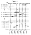
- FIG. 1 is an example frequency versus time diagram 100 for a Bluetooth® master device communicating with a slave device.
- variable length packets occupy one or more 625 us time slots in an alternating fashion, whereby a master device transmits data which begins during an even-numbered time slot noted as (E), and a slave device transmits data which begins during an odd numbered time slot noted as (O).
- E even-numbered time slot
- O odd numbered time slot
- Each packet transmission is aligned to the start of a time slot, although the packet transmission time depends on packet payload size, and may be shorter or longer than a single time slot.
- the frequency spectrum is divided into 79 channels starting with channel 0 at 2402 MHz, and each channel frequency is separated from the next by 1 MHz.
- Each packet is transmitted on a single frequency slot for the duration of the packet, which may span one or more time slots.
- packet 108 is shown as being transmitted by a slave device on channel 0 (2402 MHz), whereas packet 110 is transmitted by a master device and spans more than 2 time slots.
- the sequence of frequency hops may be governed by a pseudo random sequence known to the master and slave.
- the modulation performed for a particular packet may be either GFSK or DPSK, as will be described further below.
- FIG. 2 shows an example “basic rate” packet 200 which has a 1 Mbps data rate and uses GFSK to modulate packet data including an access code 202 , a header 204 , and a variable length payload 206 .
- FIG. 3 shows an example “enhanced data rate” (EDR) packet 300 for 2 Mbps or 3 Mbps comprising a first part 302 and a second part 304 .
- the first part 302 of the packet includes an access code 306 and header 308 modulated with GFSK, and followed by a short guard interval.
- the second part 304 of the packet includes a synchronization pattern 310 , an EDR payload 314 , and a trailer 312 , all of which are modulated using DPSK in a 4-constellation pattern for 2 Mbps or an 8-constellation pattern for 3 Mbps.
- FIGS. 4A and 4B show example frequency and amplitude plots versus time for GFSK modulation of a data sequence.
- the carrier amplitude waveform 420 is constant over the example data pattern 402 “111011001”, and the modulation frequency is offset approximately +165 Khz for a “1” and ⁇ 165 Khz for a “0” in 1 us symbol intervals.
- the use of Gaussian frequency shifts rather than discrete frequency shifts may reduce the modulation sidelobe energy which could spill from the current channel into an adjacent channel and cause interference with other devices using the adjacent frequency channels.
- FIGS. 5A and 5B show one example DPSK modulation with respect to the previous example data 402 “111011001”, where each symbol “111” “011” “001” is transmitted as one of eight differential phase shifts, which are phase shifts relative to the previous phase position.
- the Bluetooth® specification maps “111” 502 to ⁇ 3 ⁇ /4, “011” 504 to + ⁇ /2, and “001” 506 to + ⁇ /4.
- the modulation accomplishes this by transmitting the associated differential phase every 1 us, thereby accomplishing the transmission of 9 bits of data in 3 us, using the phases shown in FIG. 5A , starting from initial phase 512 .
- FIG. 5B shows waveform 514 which illustrates the amplitude of a DPSK signal versus time, according to one example.
- FIG. 6 is a diagram of one embodiment of a transceiver 600 in a communication system.
- the transceiver includes a signal processor 700 , a transmit modulator 800 , and a receiver 900 .
- the transmit modulator 800 receives a plurality of input signals from the signal processor 700 .
- the transmit modulator 800 is operable as a modulator and transmitter, and also as a local oscillator (LO) signal generator.
- LO local oscillator
- the modulator 800 generates modulated signals for transmission, and during receive time intervals, the modulator 800 generates a local oscillator (LO) signal for the receiver 900 to be used for demodulating received signals, as will be described further below.
- the modulator may adjust the LO signal to compensate for a detected difference in center frequencies between the receiving and transmitting oscillators.
- the transceiver 600 may be included in a variety of communication devices, such as personal computer (PC) 601 , laptop 602 , global positioning system (GPS) device 603 , server 604 , and mobile phone 605 . It is noted, however, that the transceiver 600 may be included in other types of electronic devices, e.g., personal digital assistants (PDAs), video game consoles, and televisions.
- the transceiver 600 transmits and receives communication signals via a network 610 , e.g., a wireless and/or wired communication network.
- the network 610 may be representative of a short-range communication network (e.g., a personal area network) and the transceiver 600 may be configured to transmit and receive Bluetooth® signals via the network 610 .
- the components described with reference to FIG. 6 are meant to be exemplary only, and are not intended to limit the invention to any specific set of components or configurations.
- one or more of the components described may be omitted, combined, modified, or additional components included, as desired.
- FIG. 7 shows a block diagram of one embodiment of a signal processor 700 for use with a modulator, e.g., transmit modulator 800 of FIG. 8 , which produces wireless signals for transmission.
- the signal processor 700 and the modulator 800 can be included within a transceiver (e.g., transceiver 600 of FIG. 6 ) operable to transmit and receive wireless signals (e.g., Bluetooth® signals) via a network.
- the signal processor 700 includes support for basic rate modulation, for which the multiplexer path is shown as (B), and enhanced data rate, for which the multiplexer path is shown as (E).
- the signal processor 700 generates a plurality of signals including a first modulation input 760 , a second modulation input 762 , and an amplitude control input 764 .
- the signal processor 700 includes a signal generator 703 for the generation of modulation signals from a link controller 701 , and a delay compensator 729 which provides time-compensated modulator input signals to the modulator 800 of FIG. 8 .
- the delay compensator 729 provides the first modulation input 760 , the second modulation input 762 , and the amplitude control input 764 to the modulator 800 of FIG. 8 .
- these signals may be asserted during the duration of a packet which may be modulated at a channel frequency fc determined by channel select input 822 .
- Basic rate GFSK packets and the GFSK first part of enhanced data rate packets are processed via the multiplexer path shown as (B) in FIG. 7 .
- the (B) inputs of multiplexers 722 and 744 may be selected, and link controller 701 may provide a stream of 1 Mb digital baseband data 702 .
- the low frequency modulator first input 760 is active along with the modulator amplitude control input 764 , which ramps up at the start of packet GFSK modulation and ramps down at the end of GFSK modulation.
- the modulator first input 760 is formed by generating a Gaussian time domain generator 718 , which may function as a lookup table (LUT), and provides a Gaussian frequency modulation waveform to multiplexer 722 .
- the Gaussian frequency modulation pulse from multiplexer 722 is interpolated by interpolator 728 crossing clock domain boundary 727 from a system clock rate, such as 64 Mhz, on a first clock domain to an external modulator clock rate on an external clock domain, such as a clock rate for use by the modulator 800 of FIG. 8 .
- the first delay 732 which is operative on the second modulation input data
- the second delay 736 which is operative on the amplitude control data
- the delay compensator 729 includes a clock interpolator 728 which provides clock adaptation from the system clock (sys_clk) domain of the signal generator 703 to the external clock (ext_clk) domain of the modulator 800 .
- the interpolator 728 may be included because the digital signal processing leading to the interpolator 728 is operative on the system clock domain, such as 64 Mhz, whereas the modulator first input signal 760 is operative on an unrelated external clock domain, which may be any frequency suitable for operation of the modulator 800 of FIG. 8 , including external clocking frequencies of 12 MHz, 13 MHz, 19.2 MHz and their multiples 24 MHz, 26 MHz, 38.4 MHz, 52 MHz, as well as 40 MHz, or an external clocking frequency within 5% of any of these frequencies.
- the amplitude output control 764 is derived from a power control 748 , which establishes a desired transmit power level.
- the GFSK ramp function 742 ramps up to the desired transmit power level at start of packet, and ramps down at end of GFSK modulation time.
- a DC offset correction is then performed via DC offset unit 746 . After DC offset unit 746 , the signal is delayed by the second delay unit 736 .
- the first delay unit 732 and the second delay unit 736 provide programmable static time delays to outputs of DC offset units 726 and 746 , respectively, to compensate for modulator path differences and signal generator path differences in the generation of the modulator control signals for the modulator 800 , and ensure time coherent alignment between the signals 760 , 762 , and 764 as viewed at the output 820 of the modulator 800 .
- a stream of 2 Mbps or 3 Mbps digital baseband data 702 is provided to PSK mapping unit 704 to map the data into phase shift keying symbols.
- a root cosine filter 706 forms the envelope shaping of the phase encoded symbols.
- a CORDIC (COordination Rotation Digital Computer) 708 transforms the phase encoded symbols comprising real and imaginary (I and Q) components into corresponding phase and amplitude outputs ( ⁇ ,A).
- a differentiator 710 generates the first derivative of phase with respect to time by subtracting adjacent digital samples to form a frequency component. The frequency component is delivered to a frequency reducer 712 which limits frequency excursions.
- the frequency reducer 712 is a 5-tap FIR with coefficients [1 1 1 1 1]/5.
- the frequency component from frequency reducer 712 is then upsample filtered by upsample FIR unit 720 .
- the signal is scaled by Kmod scale unit 724 , the DC components are added or subtracted by DC offset unit 726 to remove offsets, and the result is fed to the first delay unit 732 .
- the first delay unit 732 compensates for static processing delays so that the modulator second input 762 is time aligned to the output 820 of the modulator 800 of FIG. 8 , as described earlier.
- the modified amplitude component (A) is provided to power scaling 738 , which uses power input 748 to establish a peak amplitude envelope.
- the amplitude is upsampled using upsample FIR unit 740 , and the DC offsets may be removed by DC offset unit 746 .
- the result is then delayed by the second delay unit 736 to match the time coherency of modulator amplitude input 764 to the modulator first input 760 and modulator second input 762 , as measured at the output 820 of the modulator 800 .
- FIG. 8 shows a block diagram of one embodiment of a transmit modulator 800 including a synthesizer 801 .
- the synthesizer 801 includes a voltage controlled oscillator (VCO) 812 coupled to an optional buffer 814 , a first programmable divider 830 and a second programmable divider 824 .
- VCO voltage controlled oscillator
- the output of the second programmable divider 824 is subtracted 804 from reference clock 802 and provided to charge pump 806 to form an error voltage, such as by adding or removing charge from a capacitor.
- the charge pump 806 output is low pass filtered using a programmable low pass filter (LPF) 808 , which can be set to various bandwidths, e.g., 300 Khz.
- LPF programmable low pass filter
- the output of the LPF 808 is added 810 to the analog converted (via DAC 828 ) modulator second input 762 to generate the input voltage for the VCO 812 .
- the VCO 812 may have separate inputs responsive to the LPF 808 output and the DAC 828 output. It is further noted that the VCO 812 may be configured to operate at various frequencies, e.g., 4.8 GHz.
- the second programmable divider 824 is programmed by an output of the channel decoder 823 and the sigma-delta ( ⁇ ) modulator 826 .
- a channel select signal 822 received by channel decoder 823 may select one of the available transmission channels, e.g., one of the available Bluetooth® channels.
- the channel decoder 823 provides an integer portion to the programmable divider 824 and a fraction portion that is summed with the modulator first input 760 .
- the sum of the fractional portion and the modulator first input 760 is provided to the sigma-delta modulator 826 .
- the particular integer and fractional values may be related to the selection of the reference clock 802 (i.e., reference clock frequency), as well as the configuration of dividers 824 , 830 , and sigma-delta modulator 826 .
- the first programmable divider 830 divides the output of the optional buffer 814 .
- the first programmable divider 830 may be a dual modulus divider dividing by eight or nine as may be required to configure the output of the second programmable divider 824 to be relatively close to the approximate frequency of the reference clock 802 .
- the second modulation input 762 is converted by DAC 828 to an analog signal and added 810 to the input of VCO 812 .
- the analog signal may be applied to a separate input of the VCO 812 .
- amplitude control input 764 is converted by DAC 829 to an analog signal and applied to variable gain power amplifier (VGPA) 818 .
- VGPA variable gain power amplifier
- the buffered 814 , divided 816 (e.g., divide by 2), and amplified 818 output of the VCO 812 is provided to antenna 820 for transmission.
- the amplitude control input 764 thereby controls the amplitude of the transmitted signal.
- a modulation method referred to as two-point modulation is used, whereby the first (in this case a low frequency) modulator input 760 and the second (in this case a high frequency) modulator second input 762 are both applied to the VCO 812 on opposite sides of the LPF 808 , which changes the frequency response at the output of the modulator 800 .
- Y out H ( f )* X lf +( X hf *(1 ⁇ H ( f ))) (equation 1)
- the output Y out is the same as the input X hf (or X lf ), regardless of the filter response H(f).
- This allows GFSK and DPSK symbols to be modulated using X lf (the modulator first input 760 ) and X hf (the modulator second input 762 ) together.
- the response time of the modulator first input 760 may be governed by delays such as the LPF 808 response and sigma-delta modulator 826 delay, and first programmable divider 830 and second programmable divider 824 delays, whereas the modulator second input 762 incurs none of these delays over short term intervals.
- the amplitude of the modulation signals fed to first and second input may have a relatively greater amplitude for DPSK than for GFSK.
- the inputs may have different response time delay characteristics with respect to a signal seen at the output of the variable gain amplifier 818 .
- the response time for the first modulation input 760 (and the static channel select input 822 ) is longer than the response time for the second modulator input 762 , due, at least in part, to the delays through the interpolator 728 and the sigma-delta modulator 826 .
- the modulator 800 of FIG. 8 may also generate a quadrature local oscillator (LO) output 817 , which may be used as a local oscillator, either for mixing received signals to baseband (at channel frequency fc) or with a frequency offset from fc, such as 500 KHz, as may be required for some double conversion receivers.
- LO local oscillator
- a receiver attempts to receive a transmitted signal, distortion or error may occur if the center frequencies of receive demodulator and transmit modulation oscillators are not relatively close. This is sometimes referred to as a frequency error.
- a Bluetooth® receiver and transmitter are configured to communicate using channel 0 (2402 MHz), but the modulation oscillator in the transmitter produces a transmit signal that is not exactly centered about 2402 MHz, then the receiver may not clearly receive the transmitted signal.
- signal transmission errors may be caused by frequency differences (errors) between transmit and receive oscillator center frequencies.
- the frequency differences may be caused by differences in crystal oscillation frequencies used in crystal based oscillators, temperature affects, process variations, etc.
- the first modulation input 760 may continuously track variations in frequency error arising from the reference clock 802 variations, or variations in the remote transmitter channel center frequency. For example, if a difference of 50 KHz between center frequencies of a receive local oscillator (i.e., LO output 817 ) and a remote transmitter center frequency is detected while receiving a packet, the difference can be reduced by introducing a correction amount through the first modulation input 760 . This detected difference may be corrected during the packet reception time, and drifts in frequency may also be accommodated using the modulator first input 760 . As illustrated in FIG.
- modulator 800 for the first modulation input 760 to continuously track variations in frequency error during receive time intervals, modulator 800 includes a multiplexer 831 which receives first modulation input 760 from the signal processor 700 at one of the inputs (which is selectable during transmit time intervals), and a programmable first modulation input 761 at the other input (which is selectable during receive time intervals).
- the programmable first modulation input 761 is received from a frequency offset unit 825 .
- the frequency offset unit 825 is programmed with a frequency offset value to obtain the desired frequency offset, e.g., ⁇ 500 KHz, based on the reference frequency.
- the frequency offset unit 825 is programmable with a frequency error correction value to modify the programmable first modulation input 761 .
- the receiver 900 may program the frequency offset unit 825 via line 833 .
- the components described with reference to FIGS. 7 and 8 are meant to be exemplary only, and are not intended to limit the invention to any specific set of components or configurations.
- one or more of the components described may be omitted, combined, modified, or additional components included, as desired.
- the feedback loop of the synthesizer 801 may include additional components.
- FIG. 9 shows a block diagram of an example of a double conversion receiver 900 , also known as a Hybrid Offset Zero-IF receiver.
- a Hybrid Offset Zero-IF receiver is described in U.S. patent application Ser. No. 12/016,995 filed Jan. 18, 2008, which application is incorporated in its entirety by reference.
- the double conversion receiver 900 of FIG. 9 includes first analog mixers 908 , 910 for conversion to an intermediate frequency, such as 500 KHz, and a second digital mixer 936 for conversion to baseband.
- the first mixers 908 , 910 may use a local oscillator (LO) signal provided by the modulator 800 of FIG.
- LO local oscillator
- the second mixers 936 typically use a fixed second frequency 938 , such as 500 KHz.
- a signal such as one received by antenna 902 , is provided to a variable gain low noise amplifier (VGA) 906 , which provides the in-phase (I) and quadrature-phase components associated with the signal to mixers 908 and 910 , respectively.
- VGA variable gain low noise amplifier
- the mixers 908 and 910 receive quadrature oscillator signals such as at the channel frequency fc of the packet to be received, or at a fixed frequency offset from fc, such as 500 KHz, as shown at first local oscillator 920 .
- the quadrature local oscillator is provided by the LO output 817 shown in FIG. 8 .
- the two mixer 908 and 910 outputs are low pass filtered by LPFs 912 , 914 , and sampled for conversion to digital form by A/D converters (ADCs) 916 and 918 .
- the VGA 906 , the mixers 908 , 910 , the LPFs 912 , 914 , the ADCs 916 , 918 can be included within the analog front end (AFE) 904 of a receiver or transceiver. It is noted, however, that in other implementations the AFE 904 may include different components or additional components. For instance, in one embodiment, some or all of the components of modulator 800 for generating the LO oscillator signal 817 , which may be used as the LO oscillator 920 in the receiver 900 , can be included within the AFE 904 .
- the output from AFE 904 is filtered by LPF 922 , down sampled by down sample unit 924 , filtered by LPF 926 , and down sampled by down sample unit 928 .
- a DC removal block 930 receives the result from down sample unit 928 .
- a LPF 934 subtracts low frequency components using adder 932 , thereby producing a quadrature stream of data to second mixer 936 , which may operate at a fixed frequency, e.g., 500 KHz, provided by second local oscillator 938 .
- Double conversion systems, such as the one shown in FIG. 9 can reduce susceptibility to 1/f noise, by moving the modulation frequency components away from the DC region, thereby greatly reducing the noise components.
- a 500 KHz offset allows the 1/f noise to be placed at one edge of the first mixer output spectrum. It is noted that in some implementations other frequency offsets such as those in the range 450 KHz to 550 KHz are satisfactory, and a mixing offset over the range of 250 KHz to 750 KHz from a Bluetooth® channel frequency may be possible with some receiver performance degradation. In yet other implementations, the design may be modified to have other center frequencies, such as 1 MHz or 2 MHz.
- the second mixer 936 provides a baseband quadrature stream to a DPSK demodulator 940 and a GFSK demodulator 960 .
- the DPSK demodulator 940 uses a pulse shaping filter 942 followed by a LPF 944 and CORDIC 946 to compensate for symbol rotation due to frequency offsets, which are compensated by adder 950 .
- the resulting symbol amplitude and phase are detected by DPSK symbol detector 952 , which generates the DPSK demodulated output 953 .
- the GFSK demodulator 960 accepts the quadrature input signal stream from mixer 936 , and filters the signal using LPF 962 .
- the CORDIC 964 extracts the phase, and remove carrier offset unit 966 performs compensation of carrier offset.
- the result is provided to a GFSK symbol detector 968 , which measures differential phase changes from symbol to symbol, thereby producing demodulated output 969 .
- the receiver 900 of FIG. 9 may be implemented many different ways, including single conversion, whereby the first local oscillator 920 is at fc rather than at fc ⁇ 500 khz or other offsets. Furthermore, if the receiver 900 is a single conversion receiver, it does not include second local oscillator 938 and second mixer 936 . In various implementations, the receiver 900 may include processing in DPSK demodulator 940 or GFSK demodulator 960 for detection of static or dynamic frequency offsets from baseband with a correction signal provided to modulator first input 760 during receive intervals.
- DPSK demodulation 940 variations in baseband frequency may have a greater impact on the error rate of detected symbols, and symbol detector 952 and associated phase correction function 948 may also examine the phase output of CORDIC 946 to generate frequency offset information to provide to the modulator first input 760 during receive intervals. Additionally, the frequency offset from expected channel frequency fc may be detected over a short interval following an access code (e.g., the tail interval shown on FIG. 14 ) for a first GFSK part of a packet, or over the balance of a packet following an access code part of the packet (e.g., the tail and header intervals shown on FIG. 14 ).
- an access code e.g., the tail interval shown on FIG. 14
- the receiver 900 makes a frequency offset error measurement during a tail time and optionally through the remaining GFSK part of the packet, and may apply the frequency error correction value as a static correction to the 500 Khz offset value of the programmable modulator first input prior to the DPSK part of a packet.
- the receiver 900 may implement an algorithm that takes the highest positive and negative frequency during this period of time and calculate the average of the two peaks. The frequency offset error can then be determined once the average frequency is calculated. In another example, an average frequency is calculated during the tail interval and the frequency offset error is determined based on the average frequency calculations.
- the receiver 900 After the frequency error measurement operation, the receiver 900 provides a frequency error correction value to the programmable frequency offset unit 825 via line 833 to modify the modulator first input. As illustrated, in one implementation, the remove carrier offset unit 966 of the receiver 900 may determine the frequency offset error and provide the frequency error correction value to the programmable frequency offset unit 825 via line 833 .
- the output signal of the first LO is not centered exactly at 500 KHz, such as from the effect of a remote transmitter frequency offset, receiver performance is usually compromised.
- the first mixer output is centered below 500 KHz, DC offsets from the analog signal processing can mix into the main part of the signal, and mismatches between the in-phase and quadrature signals can start to degrade performance.
- the low-pass analog filters can degrade the signal, and more quantization noise from the high-pass noise shaping in the sigma-delta ADC can be added to the desired signal.
- the DPSK signal can be mixed down to a target of 500 KHz by the first mixer using a tunable local oscillator, and get as close to the 500 KHz target as possible.
- the first local oscillator is designed to be tunable rather than the second local oscillator because once the signal has been processed using analog circuits with an offset in frequency, the use of a second local oscillator with a compensating frequency offset may not recover the degradation caused by the analog impairments from the first mixer. Therefore, in various implementations, such as the examples shown in FIGS. 7-9 , the first local oscillator can be designed to be tunable for use with a digital second mixer which is coupled to a fixed frequency source.
- the components described with reference to FIG. 9 are meant to be exemplary only, and are not intended to limit the invention to any specific set of components or configurations.
- one or more of the components described may be omitted, combined, modified, or additional components included, as desired.
- the design of one or more of the filtering stage of the receiver 900 can be changed based on specifications.
- FIG. 10 shows a timing diagram of one example of the operation of the modulator 800 of FIG. 8 when operated as a transmitter modulator during transmit slots (shown as Tx), and as a receive local oscillator during receive slots (shown as Rx).
- the modulator 800 generates a local oscillator signal 817 with an optional offset from the channel frequency fc, for example, a 500 KHz offset.
- the packets, channels, and modulations being transmitted and received are as shown for the sequence of FIG. 1 .
- channel input 1002 contains the sequence of channel frequencies of FIG. 1 .
- modulator first input 1004 and modulator second input 1006 contain associated GFSK modulation sections and DPSK modulation sections.
- basic rate packets utilize GFSK modulation throughout the packet.
- Enhanced rate data packets utilize GFSK for a first part of the packet (e.g., the header) and DPSK for a second part of the packet.
- the amplitudes for the first and second modulator inputs are substantially equal to each other (after scaling for digital and analog path differences), and DPSK modulation amplitudes are larger than GFSK amplitudes on the first and second modulator inputs.
- the modulator 800 produces transmit modulation, and during receive time slots, the modulator 800 produces fc with an optional frequency offset, e.g., 500 KHz.
- the fc offset is produced by adding the appropriate offset value to the modulator first input 1004 .
- this offset could be produced by allowing channel input 1002 to select 500 KHz offsets from fc during receive time slots.
- FIG. 11 shows a timing diagram of one example of the modulator 800 output produced by the streams of inputs shown in FIG. 10 , corresponding to the transmission of packets shown in FIG. 1 .
- Each of the 625 us time slots contains corresponding transmit (Tx) modulation or receive (Rx) local oscillator output, such as local oscillator signal 817 of FIG. 8 .
- FIG. 12 shows a timing diagram of one example of the frequency versus time operation of the modulator 800 based on the modulator output shown in FIG. 11 .
- the timing diagram illustrates ideal frequency transitions, it is noted that during frequency transitions from a receive frame to a transmit frame (and vice verse) there is typically some settling time to settle to the new frequency.
- the modulator 800 may be powered down between receive and transmit frames (time lapse indicated by a break in the time axis).
- the modulator 800 would operate at a certain frequency during a first frame (e.g., receive frame), and after the first frame the modulator 800 would be powered down. Shortly thereafter, the modulator 800 would be turned back on for a subsequent frame (e.g., transmit frame), and the frequency would converge on its new target frequency for the frame (including some settling time).
- FIG. 13 shows a timing diagram of one example of the modulator 800 frequency control inputs and output frequency timing with respect to a transmit slot T 1 and a receive slot T 2 .
- the transmit slot T 1 lasts n*625 us and the receive slot T 2 lasts m*625 us, as described in the Bluetooth® standards.
- the channel select input 1302 is set to fc for the transmit time slot, and the modulator output frequency changes and settles to the new fc frequency in T 4 lock time interval, as shown in frequency vs time plot 1320 .
- the FSK part of the packet is modulated using the modulator first input 1304 and modulator second input 1306 .
- the FSK modulation is optionally followed by an enhanced data rate PSK part during the T 6 time interval, and an end of packet time interval T 7 , as shown in plot 1320 .
- the modulator frequency outputs are shown in summary in waveform 1308 and with additional detail in waveform 1320 .
- Waveform 1320 shows a receive guard interval T 3 (e.g., 10 us) added to a settling time interval T 8 prior to the Rx slot T 2 , when the channel select 1302 selects fc′ and an offset is added (e.g., 500 KHz) using modulator first input 1304 .
- T 3 receive guard interval
- an offset e.g., 500 KHz
- the modulator output frequency settles to the fc′ with the 500 KHz offset during time T 8 , which allows for an early packet reception T 3 as specified in the Bluetooth® specification.
- the receiver waits for a packet preamble and GFSK first part of a packet, shown in interval 1314 .
- the modulator first input 1304 provides a voltage sufficient to cause a 500 KHz offset in the modulator output frequency, while the modulator second input 1306 is set to a constant value.
- the receiver determines the frequency error for the packet being received.
- This frequency error is then added or subtracted from the offset at any time prior to the DPSK part of the modulation, e.g., the interval 1316 , which may provide sufficient time for the modulator output frequency to settle to the corrected value prior to the DPSK part of the modulation, shown as interval 1318 .
- a 500 KHz offset related to the double conversion architecture of receiver 900 of FIG. 9 may result in proper operation.
- the receiver detects that the remote transmitter frequency is offset by 50 KHz relative to the receive frequency.
- the 50 KHz error is detected during interval 1314 , applied at the end of interval 1314 , resulting in a modulator first input offset of 450 KHz.
- the DPSK packet is demodulated to baseband during interval 1318 with the 50 KHz offset removed.
- FIG. 14 is a timing diagram showing example methods for frequency offset error correction.
- an enhanced data rate packet has a first part 1430 comprising GFSK modulation of a preamble, access code, tail, and header, and a second part 1432 comprising the DPSK modulation portion of the packet.
- the header includes a TYPE field, which indicates packet type.
- the start of the packet occurs at time 1402 , and an estimation of frequency offset may be performed by a receiver, such as the one described in FIG. 9 , during the interval from 1404 to 1406 .
- the result of this frequency offset estimation may be subtracted from the first modulator input 760 as a correction value, thereby producing a corrected local oscillator frequency as was shown in FIG.
- Waveform 1412 shows a first method of correcting a receive frequency offset, whereby a frequency offset estimation is made during interval 1420 which begins after the access code part of the packet and prior to a header part of the packet (i.e., the tail interval). The estimated offset is subtracted and applied over a maximum time interval 1422 , thereby minimizing the frequency change per unit time.
- Waveform 1414 shows a second method of correcting a receive frequency offset, whereby the frequency estimation interval 1424 extends over the remainder of the first part of the packet following the access code (i.e., the tail and header intervals), and the correction is applied and settles during the guard interval 1426 .
- the second example shown in waveform 1414 benefits from the improved frequency offset measurement accuracy related to the longer measurement interval 1424 .
- the apportionment of frequency estimation interval and duration of application of the offset to the first modulator input may include longer or shorter intervals than shown in the examples.
- the frequency change may be a linear ramp, or a shaped non-linear waveform, which satisfies the requirement of measurement during a first part of a packet 1430 , and application of a frequency offset using a modulator control input such as a first input substantially prior to the second part of the packet 1432 .
- FIG. 15 is a flow diagram of one embodiment of a method for generating a local oscillator signal (e.g., LO signal 817 of FIG. 8 ) in a transceiver (e.g., transceiver 600 ) of a communication system.
- the transceiver 600 includes signal processor 700 , transmit modulator 800 , and receiver 900 .
- the transmit modulator 800 includes a synthesizer 801 and transmitter circuitry. During operation, the transmit modulator 800 receives a channel select input and a modulation input, e.g., from the signal processor 700 .
- a channel frequency is determined based on the channel select input, and an offset frequency is determined based on the modulation input.
- the transmit modulator 800 generates the local oscillator signal 817 based on the channel select input and the modulation input, and provides the local oscillator signal 817 to the receiver 900 .
- the receiver 900 may receive a communication signal from a second transmitter (e.g., laptop 602 of FIG. 6 ) in a network (e.g., network 610 ).
- the communication signal includes a first portion (i.e., the GFSK modulation portion) and a second portion (i.e., the DPSK modulation portion).
- the receiver 900 processes the first portion of the communication signal, as described above with reference to FIGS. 9-14 .
- the receiver 900 may perform frequency offset error estimation.
- a control unit of the receiver 900 which may be implemented in hardware and/or software, performs the frequency offset error estimation.
- the modulation input is modified based on the detected frequency offset error.
- the frequency of the local oscillator signal 817 is adjusted based, at least in part, on the modified modulation input to compensate for a difference in center frequencies between oscillators in the receiver 900 and the second transmitter, as described above with reference to FIGS. 6-14 .
- the depicted flow diagram(s) are examples meant to aid in understanding embodiments and should not be used to limit embodiments or limit scope of the claims.
- Embodiments may perform additional operations, fewer operations, operations in a different order, operations in parallel, and some operations differently.
- the frequency of the local oscillator signal 817 may be adjusted during processing of the first portion of the communication signal or during a guard interval between the first portion and the second portion of the communication signal.
- a delay compensator for a modulator, e.g., a polar modulator, having a plurality of modulator inputs, each modulator input having a different time response.
- the modulator provides both frequency shift keying (FSK) and phase shift keying (PSK) for use with a transmitter.
- the delay compensator compensates for signal generation and modulator path delays as well as providing clock synchronization when the modulator is operative on a different clock domain than the signal generator providing the modulator inputs, as will be further described below with reference to FIGS. 16-19 .
- the modulator operative for frequency and phase modulation has a first input which accepts modulator first input which is coupled to sigma-delta modulator, a loop filter, and a controllable oscillator (VCO), a second input which accepts modulator second input that is coupled to the VCO, and a third input which accepts modulator amplitude control input that is coupled to variable gain power amplifier (VPGA) having an input coupled to the output of the VCO.
- VPGA variable gain power amplifier
- the modulator can generate a frequency or phase modulated output using the first and second input together in a technique known as two-point modulation, and the amplitude control input for envelope generation. The response time from each modulator input to modulator output may be different.
- the modulator first input is directly provided to the modulator
- the modulator second input is provided to the modulator after a first delay
- modulator amplitude control input is provided to the modulator after a second delay.
- the first delay and second delay may each include a programmable delay counter and address counter for the generation of a memory address, with each delay counter coupled to a first memory and a second memory containing the modulator second input data and modulator amplitude control data, as will be further described below.
- FIG. 16 is a block diagram illustrating a delay compensation process implemented by the delay compensator 729 of FIG. 7 for aligning modulator input signals, according to one example.
- the delay compensator 729 introduces compensation delays 1624 into the generation of the modulator input signals to align the signals at the output of the modulator 800 , i.e., the delay compensator 729 introduces a first delay 1608 (D 1 ) into the generation of the modulator second input 762 and a second delay 1610 (D 2 ) into the generation of the modulator amplitude control input 764 .
- the signal processor delay block 1601 illustrates the signal generation path delays 1620 associated with the generation of the modulator input signals.
- the signal generation path delays 1620 include a frequency input generation delay 1602 (SGd 1 ) for the modulator first input 760 (LF path), a frequency input generation delay 1604 (SGd 2 ) for the modulator second input 762 (HF path), and an amplitude generation delay 1606 (SGd 3 ) for the modulator amplitude control input 764 (AM path).
- SGd 1 for the modulator first input 760
- HF path frequency input generation delay 1604
- SGd 3 amplitude generation delay
- the delay compensation process restores temporal coherency of signals arrival at the reference point of the modulator output by introducing compensation delays 1624 into the generation of the modulator input signals.
- FIG. 17A shows an example of a simplified amplitude versus time diagram for enhanced data rate packets, which use DPSK for modulation of successive symbols 1712 , 1714 , and 1716 , where no delay compensation is incorporated into the modulator signal paths.
- Symbols 1712 , 1714 , and 1716 are degraded in phase modulation purity within each symbol because of the delay between the first modulation input 760 and second modulation input 762 which form the inputs for the two-point modulator.
- the first and second modulator inputs should have equal arrival times at the input of the VCO 812 .
- the modulator first and second input arrive at different times, causing the degradation of modulation purity.
- delay compensation is accomplished by directly applying the modulator first input 760 from the signal generator to the modulator 800 , and delaying the modulator second input 762 after the signal generator using first delay unit 732 .
- the amount of delay for the modulator amplitude control input 764 is applied after the signal generator using second delay unit 732 , and may be based on the amplitude control input having a response at the modulator output which compensates for the delays between the first and second modulator inputs.
- Uncompensated FIG. 17A also shows inter-symbol transition times 1710 between symbols 1712 , 1714 , and 1716 , which would ideally be located between symbols and temporally centered within the root cosine amplitude envelope of Bluetooth® modulation.
- the short response time of the modulator amplitude control input 764 compared to the other modulator inputs causes the uncompensated modulation envelope 1711 to be applied by the modulator earlier than the corresponding symbol windows.
- the delay compensator 729 of FIG. 7 provides time delay compensation for the modulator second input 762 to compensate for signal generation and modulation delays experienced by the modulator first input 760 , thereby substantially achieving optimal two-point modulation.
- the delay compensator 729 also provides time delay compensation to the modulator amplitude control input 764 to synchronize the envelope of the modulation with the first and second modulator inputs as they arrive at the output of the modulator 800 .
- the modulator first input 760 has the longest time delay, i.e., the modulator first input path delay, which is calculated by adding the frequency input generation delay SGd 1 and the LF path modulator delay Md 1 .
- the compensation delays 1624 D 1 and D 2 are applied to the modulator second input 762 and amplitude control input 764 paths, respectively.
- the compensation delay D 1 for the modulator second input 762 is determined by subtracting the HF path modulator delay Md 2 and the frequency input generation delay SGd 2 from the modulator first input path delay, as shown in 1608 .
- the compensation delay D 2 1610 is similarly determined by subtracting the amplitude path modulator delay Md 3 and the amplitude generation delay SGd 3 from the modulator first input path delay, as shown in 1610 . In this manner, the modulator inputs may be synchronized in time with respect to the output of the modulator for substantially achieving optimal two-point modulation.
- FIG. 17B shows the effect of this time delay compensation at the output of the modulator 800 .
- Symbols generated with modulator delay compensation are shown as 1728 , 1730 , and 1732 , and have two-point modulation which includes compensation for the path delays, such that the phase modulation in each symbol is approximately ideal.
- root-cosine amplitude windows 1722 , 1724 , and 1726 are centered in each modulated symbol, as seen in amplitude envelope 1723 , which results in reducing the amplitude of spurious sidelobes generated by modulation transitions 1725 .
- FIG. 18 is a block diagram of one embodiment of the delay compensator 729 of FIG. 7 , shown as delay equalizer 1800 , for providing the time compensation delays 1624 shown in FIG. 16 .
- the delay equalizer 1800 accepts a system clock (sys_clk) 1830 shown as 64 MHz for the present example, and an external clock (ext_clk) 1834 shown as 26 MHz in this example.
- the external clock and system clock are independently generated clocks that are closely related in frequency by a fraction of two integers: number_of pulses_emitted_in_interval ⁇ number_of_clock_cycles_in_interval, such that fractional divider 1802 can generate from the system clock frequency an average clock signal (avg_clk) with a frequency very close to the external clock frequency.
- the fractional divider 1802 is able to produce the average clock (avg_clk) output closely matching the external clock frequency from the system clock and above integers according to:
- avg_clk ⁇ _freq s ⁇ ⁇ y ⁇ ⁇ s ⁇ ⁇ c ⁇ ⁇ l ⁇ ⁇ k * number_of ⁇ _pulses ⁇ _emitted ⁇ _in ⁇ _interval number_of ⁇ _clock ⁇ _cycles ⁇ _in ⁇ _interval
- number_of_clock_cycles_in_interval is the number of system clock cycles generated during a particular regular interval (shown as 32 in the present example), and the number_of_pulses_emitted_in_interval is an integer less than number_of_clock_cycles_in_interval (shown as 13 in the present example). It is noted, however, that in other implementations, the system clock and/or the external clock may be at various other frequencies.
- the system clock domain includes clocked registers, a FIFO, and counters shown in system clock domain boundary 1824 , including the modulator second input (HF path) 762 and modulator amplitude control input 764 , as well as all of the circuitry of the signal generator 703 shown in FIG. 7 .
- the external clock domain 1826 includes the modulator first input (LF path) 760 and the clocked modulator functions of FIG. 8 such as the sigma-delta modulator 826 , programmable divider 824 , and divider 830 .
- the delay equalizer of FIG. 18 accepts modulator first data 1832 , and modulator second input data 1833 is initialized into memory unit 1816 , such a random access memory (RAM).
- RAM random access memory
- Amplitude control data 1835 is provided to amplitude control memory unit 1818 , such as a RAM. It is noted, however, that in other embodiments the memory units 1816 and 1818 may be other types of memory. As illustrated, in one specific example, a controller 1820 may control the memory writes and reads with respect to memory units 1816 and 1818 .
- a write request (WR_DATA) 1827 is applied to the equalizer 1800 , in addition to a stream of modulator first data 1832 , which is filtered 1838 and decimated 1839 to the external clock rate 1834 , shown in this example as 26 MHz.
- the output of decimator 1839 is fed to the input side of a dual port FIFO 1806 which is clocked by avg_clk, shown in this example as 26 MHz average clock rate, as provided by the fractional divider 1802 described earlier.
- the dual port FIFO 1806 has sufficient depth to avoid underflow during intervals when the instantaneous input clock rate from the 26 MHz avg_clk is low, and to avoid overflow during intervals when the instantaneous input clock rate from the 26 MHz avg_clk is high. Furthermore, the dual port FIFO 1806 has sufficient depth to handle accumulations or depletion of data when the avg_clk generated by fractional divider 1802 is greater or less, respectively, than the external_clock 1834 rate, which regulates the rate at which data is clocked out of the dual port FIFO 1806 .
- the assertion of WR_DATA 1827 causes modulator first data 1832 to be clocked into the dual port FIFO 1806 , as well as the generation of FIFO_CTL from first synchronizer 1804 , which is clocked by the avg_clk output of fractional divider 1802 .
- the FIFO_CTL output for the first synchronizer 1804 is then provided to second synchronizer 1808 , which is clocked by the external clock 1834 to produce a START_EXT signal on the external clock domain 1826 .
- the START_EXT signal is then provided to third synchronizer 1810 , which synchronizes the START_EXT signal from the external clock domain 1826 to generate START_SYS on the system clock domain 1824 .
- the START_SYS signal is used to initiate the programmable delayed output of data stored in delay generation unit 1801 .
- modulator second input data 1833 is stored in memory 1816 and amplitude control data 1835 is stored in memory 1818 .
- the START_SYS signal starts first programmable delay counter 1814 and second programmable delay counter 1812 , which initially provide a programmable delay interval, and then provide incrementing addresses to the memory 1816 and the memory 1818 , which generate the modulator second input (HF path) data and the modulator amplitude control input, respectively, of outputs 1822 , which are accompanied by modulator first input (LF path) data.
- FIG. 19 shows an example timing diagram associated with the operation of delay equalizer 1800 of FIG. 18 .
- system clock (sys_clk) 1920 is shown as 64 MHz, which is provided to fractional divider 1802 , which in the present example generates number_of_pulses_emitted_in_interval of 13 with the number_of_clock_cycles_in_interval as 32, which produces 26 MHz average clock frequency, shown as 26_AVG 1922 .
- some inter-edge intervals of avg_clk 26_AVG 1922 are larger than others, which is important for sizing the FIFO 1806 for avoiding FIFO underflow or overflow.
- the average clock frequency output from the fractional divider 1802 should be approximately equal to the external clock frequency ext_clk 1928 .
- the start of transmission is signaled by the assertion of WR_DATA 1924 , which causes the filtered 1838 and decimated 1839 modulator first data 1832 to be clocked into the FIFO 1806 .
- the WR_DATA 1924 generates FIFO_CTL waveform 1926 from the first synchronizer 1804 using the edge of 26 _AVG waveform 1922 .
- the output of first synchronizer, shown as waveform FIFO_CTL 1926 is provided to second synchronizer 1808 which generates START_EXT 1930 from the external clock edge, which begins the clocking out of data from the FIFO 1806 , as shown in 1940 .
- the START_EXT 1930 is also provided to the third synchronizer 1810 to generate START_SYS 1934 using the system clock, thereby starting the compensation delay D 1 1944 , which is followed by the outputting of modulator second input data stored in the memory unit 1816 , and the compensation delay D 2 1948 , which is followed by the outputting of amplitude data stored in the memory unit 1818 to the amplitude control input of the modulator 800 .
- Embodiments may take the form of an entirely hardware embodiment, an entirely software embodiment (including firmware, resident software, micro-code, etc.) or an embodiment combining software and hardware aspects that may all generally be referred to herein as a “circuit,” “module” or “system.”
- embodiments may take the form of a computer program product embodied in any tangible medium of expression having computer usable program code embodied in the medium.
- the described embodiments may be provided as a computer program product, or software, that may include a machine-readable medium having stored thereon instructions, which may be used to program a computer system (or other electronic device(s)) to perform a process according to embodiments, whether presently described or not, since every conceivable variation is not enumerated herein.
- a machine readable medium includes any mechanism for storing or transmitting information in a form (e.g., software, processing application) readable by a machine (e.g., a computer).
- the machine-readable medium may include, but is not limited to, magnetic storage medium (e.g., floppy diskette); optical storage medium (e.g., CD-ROM); magneto-optical storage medium; read only memory (ROM); random access memory (RAM); erasable programmable memory (e.g., EPROM and EEPROM); flash memory; or other types of medium suitable for storing electronic instructions.
- embodiments may be embodied in an electrical, optical, acoustical or other form of propagated signal (e.g., carrier waves, infrared signals, digital signals, etc.), or wireline, wireless, or other communications medium.
- Computer program code for carrying out operations of the embodiments may be written in any combination of one or more programming languages, including an object oriented programming language (e.g., Java, Smalltalk, C++, etc.) and conventional procedural programming languages (e.g., “C” programming language).
- the program code may execute entirely on a user's computer, partly on the user's computer, as a stand-alone software package, partly on the user's computer and partly on a remote computer or entirely on the remote computer or server.
- the remote computer may be connected to the user's computer through any type of network, including a local area network (LAN), a personal area network (PAN), or a wide area network (WAN), or the connection may be made to an external computer (for example, through the Internet using an Internet Service Provider).
- LAN local area network
- PAN personal area network
- WAN wide area network
- Internet Service Provider an Internet Service Provider
Landscapes
- Transmitters (AREA)
Abstract
Description
Yout=H(f)*X lf+(X hf*(1−H(f))) (equation 1)
Claims (20)
Priority Applications (1)
| Application Number | Priority Date | Filing Date | Title |
|---|---|---|---|
| US12/172,375 US8498589B2 (en) | 2008-06-12 | 2008-07-14 | Polar modulator with path delay compensation |
Applications Claiming Priority (2)
| Application Number | Priority Date | Filing Date | Title |
|---|---|---|---|
| US6110308P | 2008-06-12 | 2008-06-12 | |
| US12/172,375 US8498589B2 (en) | 2008-06-12 | 2008-07-14 | Polar modulator with path delay compensation |
Publications (2)
| Publication Number | Publication Date |
|---|---|
| US20090311979A1 US20090311979A1 (en) | 2009-12-17 |
| US8498589B2 true US8498589B2 (en) | 2013-07-30 |
Family
ID=41415236
Family Applications (2)
| Application Number | Title | Priority Date | Filing Date |
|---|---|---|---|
| US12/172,374 Expired - Fee Related US8170494B2 (en) | 2008-06-12 | 2008-07-14 | Synthesizer and modulator for a wireless transceiver |
| US12/172,375 Expired - Fee Related US8498589B2 (en) | 2008-06-12 | 2008-07-14 | Polar modulator with path delay compensation |
Family Applications Before (1)
| Application Number | Title | Priority Date | Filing Date |
|---|---|---|---|
| US12/172,374 Expired - Fee Related US8170494B2 (en) | 2008-06-12 | 2008-07-14 | Synthesizer and modulator for a wireless transceiver |
Country Status (1)
| Country | Link |
|---|---|
| US (2) | US8170494B2 (en) |
Cited By (5)
| Publication number | Priority date | Publication date | Assignee | Title |
|---|---|---|---|---|
| US20130052972A1 (en) * | 2011-08-26 | 2013-02-28 | Intel Mobile Communications GmbH | Signal processing device and method for providing a first analog signal and a second analog signal |
| US20180110008A1 (en) * | 2016-10-19 | 2018-04-19 | Realtek Semiconductor Corp. | Radio-Frequency Module and Wireless Device |
| US9955250B2 (en) | 2013-03-14 | 2018-04-24 | Cirrus Logic, Inc. | Low-latency multi-driver adaptive noise canceling (ANC) system for a personal audio device |
| US10026388B2 (en) | 2015-08-20 | 2018-07-17 | Cirrus Logic, Inc. | Feedback adaptive noise cancellation (ANC) controller and method having a feedback response partially provided by a fixed-response filter |
| US10249284B2 (en) | 2011-06-03 | 2019-04-02 | Cirrus Logic, Inc. | Bandlimiting anti-noise in personal audio devices having adaptive noise cancellation (ANC) |
Families Citing this family (60)
| Publication number | Priority date | Publication date | Assignee | Title |
|---|---|---|---|---|
| US8132137B1 (en) * | 2007-11-10 | 2012-03-06 | Altera Corporation | Prediction of dynamic current waveform and spectrum in a semiconductor device |
| DE102008021876B4 (en) | 2008-05-02 | 2010-06-17 | Infineon Technologies Ag | A polar modulator and method for generating a polar modulated signal |
| US8170494B2 (en) * | 2008-06-12 | 2012-05-01 | Qualcomm Atheros, Inc. | Synthesizer and modulator for a wireless transceiver |
| US8374214B2 (en) * | 2009-04-13 | 2013-02-12 | Texas Instruments Incorporated | Frequency-hopping scheme |
| US8331273B2 (en) * | 2009-08-28 | 2012-12-11 | Mediatek Inc. | Communication methods employed in communication system associated with programmable communication protocols, and related transmitting methods, receiving methods and communication device |
| US8908877B2 (en) | 2010-12-03 | 2014-12-09 | Cirrus Logic, Inc. | Ear-coupling detection and adjustment of adaptive response in noise-canceling in personal audio devices |
| KR101909432B1 (en) | 2010-12-03 | 2018-10-18 | 씨러스 로직 인코포레이티드 | Oversight control of an adaptive noise canceler in a personal audio device |
| US9318094B2 (en) | 2011-06-03 | 2016-04-19 | Cirrus Logic, Inc. | Adaptive noise canceling architecture for a personal audio device |
| US8948407B2 (en) | 2011-06-03 | 2015-02-03 | Cirrus Logic, Inc. | Bandlimiting anti-noise in personal audio devices having adaptive noise cancellation (ANC) |
| US9214150B2 (en) | 2011-06-03 | 2015-12-15 | Cirrus Logic, Inc. | Continuous adaptation of secondary path adaptive response in noise-canceling personal audio devices |
| US8958571B2 (en) * | 2011-06-03 | 2015-02-17 | Cirrus Logic, Inc. | MIC covering detection in personal audio devices |
| US9325821B1 (en) * | 2011-09-30 | 2016-04-26 | Cirrus Logic, Inc. | Sidetone management in an adaptive noise canceling (ANC) system including secondary path modeling |
| WO2013069176A1 (en) * | 2011-11-09 | 2013-05-16 | 日本電気株式会社 | Transmitter, transmission method, and non-temporary computer-readable medium in which program is stored |
| US8731413B1 (en) * | 2012-01-23 | 2014-05-20 | Viasat, Inc. | DAC-based optical modulator and demodulator |
| US9142205B2 (en) | 2012-04-26 | 2015-09-22 | Cirrus Logic, Inc. | Leakage-modeling adaptive noise canceling for earspeakers |
| US9014387B2 (en) | 2012-04-26 | 2015-04-21 | Cirrus Logic, Inc. | Coordinated control of adaptive noise cancellation (ANC) among earspeaker channels |
| US9123321B2 (en) | 2012-05-10 | 2015-09-01 | Cirrus Logic, Inc. | Sequenced adaptation of anti-noise generator response and secondary path response in an adaptive noise canceling system |
| US9319781B2 (en) | 2012-05-10 | 2016-04-19 | Cirrus Logic, Inc. | Frequency and direction-dependent ambient sound handling in personal audio devices having adaptive noise cancellation (ANC) |
| US9318090B2 (en) | 2012-05-10 | 2016-04-19 | Cirrus Logic, Inc. | Downlink tone detection and adaptation of a secondary path response model in an adaptive noise canceling system |
| US9082387B2 (en) | 2012-05-10 | 2015-07-14 | Cirrus Logic, Inc. | Noise burst adaptation of secondary path adaptive response in noise-canceling personal audio devices |
| US9532139B1 (en) | 2012-09-14 | 2016-12-27 | Cirrus Logic, Inc. | Dual-microphone frequency amplitude response self-calibration |
| TWI491211B (en) * | 2012-09-28 | 2015-07-01 | Mstar Semiconductor Inc | Local oscillation generator and associated communication system and method for local oscillation generation |
| US9054642B2 (en) | 2012-11-15 | 2015-06-09 | Intel Mobile Communications GmbH | Systems and methods to provide compensated feedback phase information |
| US9107010B2 (en) | 2013-02-08 | 2015-08-11 | Cirrus Logic, Inc. | Ambient noise root mean square (RMS) detector |
| US9369798B1 (en) | 2013-03-12 | 2016-06-14 | Cirrus Logic, Inc. | Internal dynamic range control in an adaptive noise cancellation (ANC) system |
| US9215749B2 (en) | 2013-03-14 | 2015-12-15 | Cirrus Logic, Inc. | Reducing an acoustic intensity vector with adaptive noise cancellation with two error microphones |
| US9208771B2 (en) | 2013-03-15 | 2015-12-08 | Cirrus Logic, Inc. | Ambient noise-based adaptation of secondary path adaptive response in noise-canceling personal audio devices |
| US9635480B2 (en) | 2013-03-15 | 2017-04-25 | Cirrus Logic, Inc. | Speaker impedance monitoring |
| US9502020B1 (en) | 2013-03-15 | 2016-11-22 | Cirrus Logic, Inc. | Robust adaptive noise canceling (ANC) in a personal audio device |
| US9467776B2 (en) | 2013-03-15 | 2016-10-11 | Cirrus Logic, Inc. | Monitoring of speaker impedance to detect pressure applied between mobile device and ear |
| US10206032B2 (en) | 2013-04-10 | 2019-02-12 | Cirrus Logic, Inc. | Systems and methods for multi-mode adaptive noise cancellation for audio headsets |
| US9462376B2 (en) | 2013-04-16 | 2016-10-04 | Cirrus Logic, Inc. | Systems and methods for hybrid adaptive noise cancellation |
| US9460701B2 (en) | 2013-04-17 | 2016-10-04 | Cirrus Logic, Inc. | Systems and methods for adaptive noise cancellation by biasing anti-noise level |
| US9478210B2 (en) | 2013-04-17 | 2016-10-25 | Cirrus Logic, Inc. | Systems and methods for hybrid adaptive noise cancellation |
| US9578432B1 (en) | 2013-04-24 | 2017-02-21 | Cirrus Logic, Inc. | Metric and tool to evaluate secondary path design in adaptive noise cancellation systems |
| US9264808B2 (en) | 2013-06-14 | 2016-02-16 | Cirrus Logic, Inc. | Systems and methods for detection and cancellation of narrow-band noise |
| US9392364B1 (en) | 2013-08-15 | 2016-07-12 | Cirrus Logic, Inc. | Virtual microphone for adaptive noise cancellation in personal audio devices |
| US9666176B2 (en) | 2013-09-13 | 2017-05-30 | Cirrus Logic, Inc. | Systems and methods for adaptive noise cancellation by adaptively shaping internal white noise to train a secondary path |
| US9620101B1 (en) | 2013-10-08 | 2017-04-11 | Cirrus Logic, Inc. | Systems and methods for maintaining playback fidelity in an audio system with adaptive noise cancellation |
| CN105765991B (en) * | 2013-11-22 | 2019-04-19 | 卡姆鲁普股份有限公司 | Consumption meter with error correction |
| US10382864B2 (en) | 2013-12-10 | 2019-08-13 | Cirrus Logic, Inc. | Systems and methods for providing adaptive playback equalization in an audio device |
| US9704472B2 (en) | 2013-12-10 | 2017-07-11 | Cirrus Logic, Inc. | Systems and methods for sharing secondary path information between audio channels in an adaptive noise cancellation system |
| US10219071B2 (en) | 2013-12-10 | 2019-02-26 | Cirrus Logic, Inc. | Systems and methods for bandlimiting anti-noise in personal audio devices having adaptive noise cancellation |
| US9369557B2 (en) | 2014-03-05 | 2016-06-14 | Cirrus Logic, Inc. | Frequency-dependent sidetone calibration |
| US9479860B2 (en) | 2014-03-07 | 2016-10-25 | Cirrus Logic, Inc. | Systems and methods for enhancing performance of audio transducer based on detection of transducer status |
| US9648410B1 (en) | 2014-03-12 | 2017-05-09 | Cirrus Logic, Inc. | Control of audio output of headphone earbuds based on the environment around the headphone earbuds |
| US9319784B2 (en) | 2014-04-14 | 2016-04-19 | Cirrus Logic, Inc. | Frequency-shaped noise-based adaptation of secondary path adaptive response in noise-canceling personal audio devices |
| US9609416B2 (en) | 2014-06-09 | 2017-03-28 | Cirrus Logic, Inc. | Headphone responsive to optical signaling |
| US10181315B2 (en) | 2014-06-13 | 2019-01-15 | Cirrus Logic, Inc. | Systems and methods for selectively enabling and disabling adaptation of an adaptive noise cancellation system |
| US9197258B1 (en) * | 2014-06-13 | 2015-11-24 | Intel IP Corporation | System and method for generating a data dependent clock for a DAC in a modulator |
| US9478212B1 (en) | 2014-09-03 | 2016-10-25 | Cirrus Logic, Inc. | Systems and methods for use of adaptive secondary path estimate to control equalization in an audio device |
| US9552805B2 (en) | 2014-12-19 | 2017-01-24 | Cirrus Logic, Inc. | Systems and methods for performance and stability control for feedback adaptive noise cancellation |
| US10094705B2 (en) * | 2014-12-29 | 2018-10-09 | Solid, Inc. | Apparatus and method for processing output signal of analog-to-digital converter |
| US9578415B1 (en) | 2015-08-21 | 2017-02-21 | Cirrus Logic, Inc. | Hybrid adaptive noise cancellation system with filtered error microphone signal |
| US10013966B2 (en) | 2016-03-15 | 2018-07-03 | Cirrus Logic, Inc. | Systems and methods for adaptive active noise cancellation for multiple-driver personal audio device |
| EP3264220B1 (en) * | 2016-07-01 | 2019-02-20 | Intel IP Corporation | Radio frequency signal synthesizer circuit and method for generating a radio frequency signal |
| CN108737320B (en) * | 2017-04-19 | 2020-10-23 | 博通集成电路(上海)股份有限公司 | Transmitter and method for transmitting Bluetooth data packet |
| JP7204627B2 (en) * | 2019-10-11 | 2023-01-16 | 株式会社東芝 | wireless communication device |
| CN114336881B (en) * | 2022-01-05 | 2023-08-29 | 南方电网电力科技股份有限公司 | Battery management active equalization down-conversion control method and related device |
| CN117492049B (en) * | 2023-12-29 | 2024-04-02 | 中国人民解放军国防科技大学 | High-precision timing method and device under anti-interference conditions |
Citations (14)
| Publication number | Priority date | Publication date | Assignee | Title |
|---|---|---|---|---|
| US20040183601A1 (en) | 2003-03-17 | 2004-09-23 | Xiaopin Zhang | Maximally digitized fractional-N frequency synthesizer and modulator with maximal fractional spurs removing |
| US6873836B1 (en) | 1999-03-03 | 2005-03-29 | Parkervision, Inc. | Universal platform module and methods and apparatuses relating thereto enabled by universal frequency translation technology |
| US20050245208A1 (en) * | 2004-03-03 | 2005-11-03 | Matsushita Electric Industrial Co., Ltd. | Polar modulation transmission apparatus and radio communication apparatus |
| US20060057976A1 (en) * | 2004-09-14 | 2006-03-16 | Nikolaus Klemmer | Delay calibration in polar modulation transmitters |
| US20060116091A1 (en) | 2004-11-02 | 2006-06-01 | Markus Hammes | Radio receiver for the reception of data bursts which are modulated with two modulation types |
| US20060246856A1 (en) * | 2003-08-07 | 2006-11-02 | Matsushita Electric Industrial Co., Ltd | Transmitter apparatus |
| US20070142005A1 (en) * | 2005-12-20 | 2007-06-21 | Lars Sundstrom | Method and apparatus for modulation path delay mismatch compensation in a polar modulation transmitter |
| US20080002788A1 (en) | 2005-08-11 | 2008-01-03 | Texas Instruments Inc. | Local oscillator incorporating phase command exception handling utilizing a quadrature switch |
| US20080026706A1 (en) * | 2005-04-28 | 2008-01-31 | Matsushita Electric Industrial Co., Ltd. | Polar Modulating Circuit, Polar Coordinate Modulating Method, Integrated Circuit and Radio Transmission Device |
| US7372917B2 (en) * | 2004-08-25 | 2008-05-13 | Broadcom Corporation | Digital algorithm for on-line ACPR optimization in polar RF transmitters |
| US20090203327A1 (en) * | 2008-02-07 | 2009-08-13 | Broadcom Corporation | Rf polar transmitter and integrated circuit with programmable baseband filtering and methods for use therewith |
| US20090311972A1 (en) | 2008-06-12 | 2009-12-17 | Atheros Communications, Inc. | Synthesizer and modulator for a wireless transceiver |
| US7869541B2 (en) * | 2006-11-17 | 2011-01-11 | Broadcom Corporation | Method and system for direct and polar modulation using a two input PLL |
| US8050637B2 (en) * | 2005-12-27 | 2011-11-01 | Panasonic Corporation | Polar modulation transmitter, adaptive distortion compensation processing system, polar modulation transmission method, and adaptive distortion compensation processing method |
Family Cites Families (3)
| Publication number | Priority date | Publication date | Assignee | Title |
|---|---|---|---|---|
| US116091A (en) * | 1871-06-20 | Improvement in cut-nail machines | ||
| US2788A (en) * | 1842-09-23 | Chaeles lyon | ||
| US183601A (en) * | 1876-10-24 | Improvement in devices for securing metallic fence-rails to posts |
-
2008
- 2008-07-14 US US12/172,374 patent/US8170494B2/en not_active Expired - Fee Related
- 2008-07-14 US US12/172,375 patent/US8498589B2/en not_active Expired - Fee Related
Patent Citations (17)
| Publication number | Priority date | Publication date | Assignee | Title |
|---|---|---|---|---|
| US6873836B1 (en) | 1999-03-03 | 2005-03-29 | Parkervision, Inc. | Universal platform module and methods and apparatuses relating thereto enabled by universal frequency translation technology |
| US20040183601A1 (en) | 2003-03-17 | 2004-09-23 | Xiaopin Zhang | Maximally digitized fractional-N frequency synthesizer and modulator with maximal fractional spurs removing |
| US20060246856A1 (en) * | 2003-08-07 | 2006-11-02 | Matsushita Electric Industrial Co., Ltd | Transmitter apparatus |
| US7333780B2 (en) * | 2004-03-03 | 2008-02-19 | Matsushita Electric Industrial Co., Ltd. | Polar modulation transmission apparatus and radio communication apparatus |
| US20050245208A1 (en) * | 2004-03-03 | 2005-11-03 | Matsushita Electric Industrial Co., Ltd. | Polar modulation transmission apparatus and radio communication apparatus |
| US7372917B2 (en) * | 2004-08-25 | 2008-05-13 | Broadcom Corporation | Digital algorithm for on-line ACPR optimization in polar RF transmitters |
| US20060057976A1 (en) * | 2004-09-14 | 2006-03-16 | Nikolaus Klemmer | Delay calibration in polar modulation transmitters |
| US7359680B2 (en) * | 2004-09-14 | 2008-04-15 | Telefonaktiebolaget Lm Ericsson (Publ) | Delay calibration in polar modulation transmitters |
| US20060116091A1 (en) | 2004-11-02 | 2006-06-01 | Markus Hammes | Radio receiver for the reception of data bursts which are modulated with two modulation types |
| US20080026706A1 (en) * | 2005-04-28 | 2008-01-31 | Matsushita Electric Industrial Co., Ltd. | Polar Modulating Circuit, Polar Coordinate Modulating Method, Integrated Circuit and Radio Transmission Device |
| US7715808B2 (en) * | 2005-04-28 | 2010-05-11 | Panasonic Corporation | Polar modulating circuit, polar coordinate modulating method, integrated circuit and radio transmission device |
| US20080002788A1 (en) | 2005-08-11 | 2008-01-03 | Texas Instruments Inc. | Local oscillator incorporating phase command exception handling utilizing a quadrature switch |
| US20070142005A1 (en) * | 2005-12-20 | 2007-06-21 | Lars Sundstrom | Method and apparatus for modulation path delay mismatch compensation in a polar modulation transmitter |
| US8050637B2 (en) * | 2005-12-27 | 2011-11-01 | Panasonic Corporation | Polar modulation transmitter, adaptive distortion compensation processing system, polar modulation transmission method, and adaptive distortion compensation processing method |
| US7869541B2 (en) * | 2006-11-17 | 2011-01-11 | Broadcom Corporation | Method and system for direct and polar modulation using a two input PLL |
| US20090203327A1 (en) * | 2008-02-07 | 2009-08-13 | Broadcom Corporation | Rf polar transmitter and integrated circuit with programmable baseband filtering and methods for use therewith |
| US20090311972A1 (en) | 2008-06-12 | 2009-12-17 | Atheros Communications, Inc. | Synthesizer and modulator for a wireless transceiver |
Non-Patent Citations (4)
| Title |
|---|
| "U.S. Appl. No. 12/172,374 Final Office Action", Sep. 23, 2011, 15 pages. |
| "U.S. Appl. No. 12/172,374 Office Action", Feb. 24, 2011, 13 pages. |
| U.S. Appl. No. 12/016,955, filed Jan. 18, 2008, Husted, Paul J., et al. |
| U.S. Appl. No. 12/172,374, filed Jul. 14, 2008, Husted, Paul J., et al. |
Cited By (8)
| Publication number | Priority date | Publication date | Assignee | Title |
|---|---|---|---|---|
| US10249284B2 (en) | 2011-06-03 | 2019-04-02 | Cirrus Logic, Inc. | Bandlimiting anti-noise in personal audio devices having adaptive noise cancellation (ANC) |
| US20130052972A1 (en) * | 2011-08-26 | 2013-02-28 | Intel Mobile Communications GmbH | Signal processing device and method for providing a first analog signal and a second analog signal |
| US8761697B2 (en) * | 2011-08-26 | 2014-06-24 | Intel Mobile Communications GmbH | Signal processing device and method for providing a first analog signal and a second analog signal |
| US9955250B2 (en) | 2013-03-14 | 2018-04-24 | Cirrus Logic, Inc. | Low-latency multi-driver adaptive noise canceling (ANC) system for a personal audio device |
| US10026388B2 (en) | 2015-08-20 | 2018-07-17 | Cirrus Logic, Inc. | Feedback adaptive noise cancellation (ANC) controller and method having a feedback response partially provided by a fixed-response filter |
| US20180110008A1 (en) * | 2016-10-19 | 2018-04-19 | Realtek Semiconductor Corp. | Radio-Frequency Module and Wireless Device |
| US10064140B2 (en) * | 2016-10-19 | 2018-08-28 | Realtek Semiconductor Corp. | Radio-frequency module and wireless device |
| US10462747B2 (en) | 2016-10-19 | 2019-10-29 | Realtek Semiconductor Corp. | Radio-frequency module and wireless device |
Also Published As
| Publication number | Publication date |
|---|---|
| US20090311979A1 (en) | 2009-12-17 |
| US8170494B2 (en) | 2012-05-01 |
| US20090311972A1 (en) | 2009-12-17 |
Similar Documents
| Publication | Publication Date | Title |
|---|---|---|
| US8498589B2 (en) | Polar modulator with path delay compensation | |
| US7333582B2 (en) | Two-point frequency modulation apparatus, wireless transmitting apparatus, and wireless receiving apparatus | |
| US8155235B2 (en) | Modulation device and demodulation device | |
| US10516521B2 (en) | Sampling rate synchronization between transmitters and receivers | |
| US8130865B2 (en) | Digital modulation jitter compensation for polar transmitter | |
| WO2006118056A1 (en) | Two-point modulation type phase modulating apparatus, polar modulation transmitting apparatus, radio transmitting apparatus, and wireless communication apparatus | |
| US7577219B2 (en) | Apparatus for communications | |
| US8258826B2 (en) | Automatic frequency control circuit | |
| JPH0951296A (en) | Cross polarization compensation method and cross polarization compensation device | |
| US7502435B2 (en) | Two-point modulator arrangement and use thereof in a transmission arrangement and in a reception arrangement | |
| US5200977A (en) | Terminal unit apparatus for time division multiplexing access communications system | |
| JP5354293B2 (en) | Phase synchronization apparatus and phase synchronization method | |
| EP2627053B1 (en) | Polar modulation | |
| JP2006504368A (en) | Method for removing DC offset for zero intermediate frequency based GSM radio receiver with digital frequency offset correction | |
| JP2006504368A5 (en) | ||
| US8144811B2 (en) | Hybrid zero-IF receiver | |
| CN101366219A (en) | pulse radio receiver | |
| CN105846844B (en) | Receiving apparatus and receiving method of receiving apparatus | |
| JP4214635B2 (en) | Digital radio equipment | |
| JPH10210092A (en) | Phase detection circuit | |
| KR100910885B1 (en) | Digital modulator | |
| JP2003529956A (en) | Multiplier for multiplying complex signals | |
| EP1303074A2 (en) | Symbol synchronisation in EDGE handsets | |
| JP2003110639A (en) | Multi-rate receiver | |
| JPS6360652A (en) | Demodulation circuit |
Legal Events
| Date | Code | Title | Description |
|---|---|---|---|
| AS | Assignment |
Owner name: ATHEROS COMMUNICATIONS, INC., CALIFORNIA Free format text: ASSIGNMENT OF ASSIGNORS INTEREST;ASSIGNORS:HUSTED, PAUL J.;SI, WILLIAM W.;WEBER, DAVID J.;AND OTHERS;SIGNING DATES FROM 20080728 TO 20080808;REEL/FRAME:021583/0716 |
|
| AS | Assignment |
Owner name: QUALCOMM, INCORPORATED, CALIFORNIA Free format text: MERGER;ASSIGNOR:ATHEROS COMMUNICATIONS, INC.;REEL/FRAME:026763/0770 Effective date: 20110524 |
|
| AS | Assignment |
Owner name: QUALCOMM ATHEROS, INC., CALIFORNIA Free format text: CORRECTIVE ASSIGNMENT TO CORRECT THE RECEIVING PARTY PREVIOUSLY RECORDED ON REEL 026763 FRAME 0770. ASSIGNOR(S) HEREBY CONFIRMS THE MERGER;ASSIGNOR:ATHEROS COMMUNICATIONS, INC.;REEL/FRAME:026770/0064 Effective date: 20110524 |
|
| AS | Assignment |
Owner name: QUALCOMM INCORPORATED, CALIFORNIA Free format text: ASSIGNMENT OF ASSIGNORS INTEREST;ASSIGNOR:QUALCOMM ATHEROS, INC.;REEL/FRAME:029385/0104 Effective date: 20121022 |
|
| FEPP | Fee payment procedure |
Free format text: PAYOR NUMBER ASSIGNED (ORIGINAL EVENT CODE: ASPN); ENTITY STATUS OF PATENT OWNER: LARGE ENTITY |
|
| REMI | Maintenance fee reminder mailed | ||
| LAPS | Lapse for failure to pay maintenance fees |
Free format text: PATENT EXPIRED FOR FAILURE TO PAY MAINTENANCE FEES (ORIGINAL EVENT CODE: EXP.) |
|
| STCH | Information on status: patent discontinuation |
Free format text: PATENT EXPIRED DUE TO NONPAYMENT OF MAINTENANCE FEES UNDER 37 CFR 1.362 |
|
| FP | Lapsed due to failure to pay maintenance fee |
Effective date: 20170730 |