US8411998B2 - Method and apparatus providing perspective correction and/or image dewarping - Google Patents
Method and apparatus providing perspective correction and/or image dewarping Download PDFInfo
- Publication number
- US8411998B2 US8411998B2 US12/222,950 US22295008A US8411998B2 US 8411998 B2 US8411998 B2 US 8411998B2 US 22295008 A US22295008 A US 22295008A US 8411998 B2 US8411998 B2 US 8411998B2
- Authority
- US
- United States
- Prior art keywords
- horizontal
- output
- vertical
- index
- address
- Prior art date
- Legal status (The legal status is an assumption and is not a legal conclusion. Google has not performed a legal analysis and makes no representation as to the accuracy of the status listed.)
- Active, expires
Links
- 238000012937 correction Methods 0.000 title claims abstract description 41
- 238000000034 method Methods 0.000 title claims abstract description 24
- 238000013507 mapping Methods 0.000 claims abstract description 104
- 238000012545 processing Methods 0.000 claims abstract description 29
- 230000003287 optical effect Effects 0.000 claims description 71
- 238000003384 imaging method Methods 0.000 claims description 23
- 230000006870 function Effects 0.000 description 64
- 230000000875 corresponding effect Effects 0.000 description 27
- 238000010586 diagram Methods 0.000 description 14
- 238000004377 microelectronic Methods 0.000 description 4
- 230000008569 process Effects 0.000 description 4
- 239000004065 semiconductor Substances 0.000 description 3
- 230000004044 response Effects 0.000 description 2
- 238000005070 sampling Methods 0.000 description 2
- 238000012935 Averaging Methods 0.000 description 1
- 238000007792 addition Methods 0.000 description 1
- 238000001444 catalytic combustion detection Methods 0.000 description 1
- 230000001413 cellular effect Effects 0.000 description 1
- 230000008859 change Effects 0.000 description 1
- 230000000295 complement effect Effects 0.000 description 1
- 230000002596 correlated effect Effects 0.000 description 1
- 238000012217 deletion Methods 0.000 description 1
- 230000037430 deletion Effects 0.000 description 1
- 238000013461 design Methods 0.000 description 1
- 238000001514 detection method Methods 0.000 description 1
- 230000000694 effects Effects 0.000 description 1
- 238000005516 engineering process Methods 0.000 description 1
- 230000010354 integration Effects 0.000 description 1
- 238000004519 manufacturing process Methods 0.000 description 1
- 229910044991 metal oxide Inorganic materials 0.000 description 1
- 150000004706 metal oxides Chemical class 0.000 description 1
- 238000012986 modification Methods 0.000 description 1
- 230000004048 modification Effects 0.000 description 1
- 230000006641 stabilisation Effects 0.000 description 1
- 238000011105 stabilization Methods 0.000 description 1
- 238000006467 substitution reaction Methods 0.000 description 1
Images


Classifications
-
- G—PHYSICS
- G06—COMPUTING; CALCULATING OR COUNTING
- G06T—IMAGE DATA PROCESSING OR GENERATION, IN GENERAL
- G06T3/00—Geometric image transformations in the plane of the image
-
- H—ELECTRICITY
- H04—ELECTRIC COMMUNICATION TECHNIQUE
- H04N—PICTORIAL COMMUNICATION, e.g. TELEVISION
- H04N5/00—Details of television systems
- H04N5/222—Studio circuitry; Studio devices; Studio equipment
- H04N5/262—Studio circuits, e.g. for mixing, switching-over, change of character of image, other special effects ; Cameras specially adapted for the electronic generation of special effects
- H04N5/2628—Alteration of picture size, shape, position or orientation, e.g. zooming, rotation, rolling, perspective, translation
Definitions
- the embodiments described herein relate generally to the field of digital image processing, and more specifically to methods and apparatuses providing for dewarping and/or perspective correction of a captured digital image.
- Microelectronic imaging devices are used in digital cameras, wireless devices with picture capabilities, and many other applications.
- PDAs personal digital assistants
- the growth rate of microelectronic imaging devices has been steadily increasing as they become smaller and produce better images having higher pixel counts.
- Microelectronic imaging devices include image sensors that use charged coupled device (CCD) systems, complementary metal-oxide semiconductor (CMOS) systems or other imager technology.
- CCD image sensors have been widely used in digital cameras and other applications.
- CMOS image sensors are also popular because they have low production costs, high yields, and small sizes.
- a camera system uses at least one lens to focus one or more images of a scene to be captured by an imaging device.
- the imaging device includes a pixel array that comprises a plurality of photosensitive pixels arranged in a predetermined number of columns and rows. Each pixel in the array typically has an individual assigned address.
- a lens focuses light on the pixels of the pixel array, which then generate signals representing incident light. These signals are then processed to produce an output image.
- FIG. 1A illustrates an input image 110 .
- Input image 110 includes lines 116 and a rectangular object 118 .
- Input image 110 has warping (e.g., lines 116 , that in reality are straight, appear to be curved).
- Warping in a captured image 110 can be corrected through non-linear image processing (known as “dewarping”).
- FIG. 1B illustrates a corrected (i.e., “dewarped”) image 112 , in which the lines 116 from the scene which appeared curved in the captured image 110 ( FIG. 1A ) now appear straight.
- image processing can be used to make it appear as though the camera is capturing the image from a position further away from the viewer and looking at the scene from a more downward angle, reducing the effect of perspective causing lines to appear as though they converge in the distance.
- the side edges of the rectangular object 118 appear to converge away from the camera in the dewarped image 112 of FIG. 1B .
- FIG. 1C illustrates a perspective-corrected and dewarped image 114 .
- Perspective-corrected and dewarped image 114 can be generated by applying further image processing to dewarped image 112 ( FIG. 1B ). Based on the layout in the perspective-corrected image 114 , the camera appears to have been in a different location from the one used to take the warped and dewarped images 110 , 112 , relative to the rectangular object 118 . The side edges of the rectangular object 118 also no longer appear to converge, but rather are parallel.
- Dewarping and perspective correction may require significant processing of the input image 110 . Further, the processing may require large amounts of hardware to implement. Accordingly, there is a need and desire for a spatially and temporally efficient method for providing dewarping and/or perspective correction of an image.
- FIG. 1A illustrates a captured image
- FIG. 1B illustrates a dewarped image generated from the captured image of FIG. 1A .
- FIG. 1C illustrates a perspective-corrected image generated from the dewarped image of FIG. 1B .
- FIG. 2 is a block diagram of an image processor with address mapping, in accordance with a first embodiment of the present invention.
- FIG. 3 is a block diagram of an image processor with address mapping and an interpolation filter, in accordance with a second embodiment of the present invention.
- FIG. 4 is a functional diagram of a first embodiment of an address mapping function.
- FIG. 5 is a diagram showing examples of pixel locations of an input and output image.
- FIG. 6 is a functional diagram of a second embodiment of an address mapping function.
- FIG. 7 is a functional diagram of a third embodiment of an address mapping function.
- FIG. 8 is a functional diagram of a polynomial function generator.
- FIG. 9 is an imaging device coupled to an image processor, in accordance with an embodiment described herein.
- FIG. 10 is a system implementing an image processor in accordance with an embodiment described herein.
- Embodiments described herein perform the dewarping and/or perspective correction shown in FIGS. 1A through 1C by rearranging portions of captured image 110 according to processing described herein.
- Pixel values of captured image 110 or functions thereof, are mapped onto corresponding locations of dewarped and perspective-corrected image 114 .
- This mapping of a value for a desired output pixel location from one or more input pixel locations, while accounting for desired dewarping and/or perspective correction, is implemented using a single level of processing, described herein.
- space-efficient implementations of imager and image processing components are disclosed. These efficiencies can help achieve smaller camera systems.
- the size of the image processing circuitry is of paramount concern.
- FIG. 2 illustrates a block diagram of a first embodiment of an image processor 200 for implementing dewarping and/or perspective correction.
- Image processor 200 includes a buffer 224 , an output address generator 220 , and an address mapping unit 222 .
- Image processor 200 receives a plurality of lines of pixel values f i (x, y) from an input image that may have warping and is captured from a first perspective (e.g., captured image 110 of FIG. 1A ), and outputs individual output pixel values f o (x o , y o ) of an output image that is dewarped and/or perspective-corrected (e.g., dewarped and perspective-corrected image 114 of FIG. 1C ).
- the buffer 224 acts as a storage circuit for the plurality of lines of pixel values f i (x, y), and outputs pixel values according to the address mapping unit 222 .
- an output pixel value f o (x o , y o ) for an output pixel address (x o , y o ) in the output image is determined from a stored input pixel value f i (x int , y int ) from the input image.
- address mapping unit 222 For each output pixel address (x o , y o ) in the output image, address mapping unit 222 calculates horizontal and vertical input indexes x i , y i indicating a corresponding input pixel address (x int , y int ) associated with an input pixel value f i (x int , y int ) stored in buffer 220 to be placed at the output pixel address (x o , y o ).
- address mapping unit 222 uses received parameters, discussed below, to determine the amount of radial gain (i.e., horizontal and vertical scaling) applied to the output pixel address (x o , y o ) in order to account for warping in the input image, and the amount of horizontal gain (i.e., horizontal scaling) and vertical offset (i.e., vertical shifting) to be applied to the output pixel address (x o , y o ) in order to account for variation between the desired perspective in the output image and the original perspective in the captured image.
- radial gain i.e., horizontal and vertical scaling
- horizontal and vertical offset i.e., vertical shifting
- address mapping unit 222 calculates and outputs horizontal and vertical indexes x i , y i as integer values x int , y int .
- the indexes x int , y int are transmitted to the buffer 224 , which outputs the corresponding input pixel value f i (x int , y int ) as output pixel value f o (x o , y o ) to a storage device, e.g., a random access memory 1094 ( FIG. 10 ).
- pixel values of an image are organized as a grid of (M ⁇ N) coordinates.
- Each input pixel value f i (x, y) and output pixel value f o (x, y) is assigned a corresponding pixel address of Cartesian coordinates (x M , y N ) measured from the top left corner of the grid.
- the horizontal and vertical indexes x, y of the input pixel address are integer values.
- the horizontal and vertical input indexes x i , y i calculated by the address mapping unit 222 are integer values x int , y int .
- the input and output images may have differing numbers of pixels (i.e., different values of M and N), and thus different center addresses.
- the potential difference between center pixel addresses of the input image 110 and the output image 114 can be accounted for by performing image processing on the offset of the respective horizontal and vertical indexes (i.e., calculating how far the corresponding horizontal and vertical input indexes x i , y i are from the center of the captured image 110 ), as described further below.
- the corresponding input pixel address (x int , y int ) represents a portion of the captured image which, after dewarping and perspective correction, properly belongs at the output pixel address (x o , y o ).
- each pixel address of the output image had a corresponding input pixel address in the captured image 110 , the corresponding input pixel address being determined by address mapping unit 220 .
- the pixel addresses of the pixels showing the lines 116 would be approximately vertical, yet their pixel value would be determined from a corresponding pixel address constituting the curved edges of lines 116 in captured image 110 .
- FIG. 3 illustrates a block diagram of a second embodiment of an image processor 300 , in accordance with an embodiment for implementing dewarping and perspective correction as described herein.
- Image processor 300 also includes a buffer 324 , an output address generator 320 , and an address mapping unit 322 .
- Image processor 300 further includes an interpolation filter 326 .
- the interpolation filter 326 and buffer 320 act as a storage circuit for the plurality of lines of pixel values f i (x, y), and output pixel values according to the address mapping unit 322 .
- address mapping unit 222 of image processor 200 FIG.
- address mapping unit 322 calculates horizontal and vertical input indexes x i , y i indicating a corresponding input pixel address (x int , y int ) associated with an input pixel value f i (x int , y int ) stored in buffer 320 to be placed at the output pixel address (x o , y o ). Also like address mapping unit 222 of image processor 200 ( FIG.
- address mapping unit 322 uses received parameters, discussed below, to determine the amount of radial gain (i.e., horizontal and vertical scaling) applied to the output pixel address (x o , y o ) in order to account for warping in the input image, and the amount of horizontal gain (i.e., horizontal scaling) and vertical offset (i.e., vertical shifting) to be applied to the output pixel address (x o , y o ) in order to account for variation between the desired perspective in the output image and the original perspective in the captured image.
- radial gain i.e., horizontal and vertical scaling
- horizontal gain and vertical offset i.e., vertical shifting
- the horizontal and vertical indexes x i , y i are calculated by address mapping unit 322 as scaled floating point numbers with integer components x int , y int and fractional components x fraction , y fraction .
- the integer components x int , y int are transmitted from address mapping unit 322 to buffer 324 , which outputs the corresponding input pixel value f i (x int , y int ).
- buffer 324 In addition to outputting the corresponding input pixel value f i (x int , y int ), buffer 324 also outputs to interpolation filter 326 pixel values corresponding to a plurality of neighboring input pixel addresses.
- the fractional components x fraction , y fraction are output from address mapping unit 322 to interpolation filter 326 .
- Interpolation filter 326 calculates an output pixel value f o (x o , y o ) corresponding to the output pixel address (x o , y o ) as a function of the determined input pixel value f i (x int , y int ) and the neighboring pixel values, according to the fractional components x fraction , y fraction .
- interpolation filter 326 may interpolate the pixel values output by buffer 324 , giving weight to each pixel value according to the fractional components x fraction , y fraction .
- the interpolation filter 326 outputs the calculated output pixel value f o (x o , y o ) to a storage device, e.g., random access memory 1094 ( FIG. 10 ).
- the integer components x int , y int and fractional components x fraction , y fraction of the horizontal and vertical indexes x i , y i calculated by address mapping unit 322 may be separated at the output of address mapping unit 322 , according to any known methods (e.g., integer and component filters).
- the entire scaled floating point values of horizontal and vertical indexes x i , y i may be output by address mapping unit 322 to both buffer 324 and interpolation filter 326 , and the inputs of buffer 324 and interpolation filter 326 may each filter the received horizontal and vertical indexes x i , y i to receive the appropriate components.
- address mapping unit 322 may instead calculate the horizontal and vertical indexes x i , y i as integer values (x int , y int ), and calculate the output pixel value f o (x o , y o ) according to pre-determined processes.
- address mapping unit 322 communicates the horizontal and vertical indexes x i , y i to buffer 324 .
- Buffer 324 outputs the corresponding input pixel value f i (x int , y int ) and the input pixel values corresponding to a plurality of neighboring input pixel addresses to interpolation filter 326 .
- interpolation filter 326 calculates an output pixel value f o (x o , y o ) according to pre-determined processes, such as averaging of the pixel values output by buffer 324 , and outputs f o (x o , y o ) to a storage device, e.g., random access memory 1094 ( FIG. 10 ).
- FIG. 4 shows a functional diagram of a first embodiment of an address mapping unit 400 that can be used in the image processor 300 described above.
- Address mapping unit 400 determines the horizontal and vertical indexes x i , y i corresponding to an input pixel address (x int , y int ) of the input image f i (x, y) stored in the buffer 324 ( FIG. 3 ).
- the pixel value stored at the input pixel address (x int , y int ) is used to determine the pixel value corresponding to the desired output pixel address (x o , y o ), allowing for dewarping and perspective correction of the input image.
- the address mapping unit 400 implements perspective correction with linear scaling horizontally about the center of the image, and shifting vertically.
- Address mapping unit 400 calculates corresponding input address indexes x i , y i as described below.
- the input address indexes x i , y i are calculated as scaled floating point values having integer components x int , y int and fractional components x fraction , y fraction , such as for use in image processor 300 ( FIG. 3 ).
- the input address indexes x i , y i may be calculated as integer values, such as for use with image processor 200 ( FIG. 2 ), or with other embodiments of an image processor with an address mapping unit which does not use fractional components x fraction , y fraction .
- the horizontal index polynomial function generator 430 , vertical index polynomial function generator 432 , and radial gain polynomial function generator 434 may be configured such that their respective outputs are integer values.
- Address mapping unit 400 receives the horizontal and vertical output indexes x o , y o from the output address generator 320 ( FIG. 3 ). Address mapping unit 400 also receives three sets of polynomial function coefficients: horizontal index polynomial coefficients P x ; vertical index polynomial coefficients P y ; and radial gain polynomial coefficients P r . Horizontal index polynomial coefficients P x are used by address mapping unit 400 to calculate the horizontal gain g x , in order to account for the horizontal scaling of perspective correction. Vertical index polynomial coefficients P y are used by address mapping unit 400 to calculate the vertical offset y P , in order to account for the vertical shifting of perspective correction. Radial gain polynomial coefficients P r are used by address mapping unit 400 to calculate the radial gain g r , in order to account for the horizontal and vertical scaling of dewarping.
- the sets of polynomial function coefficients P x , P y , P r may be input from an external program or a user, or may be pre-programmed in address mapping unit 400 as based on known dewarping and perspective correction values for a particular imaging system, or for a desired result. For example, it may be desirable to input horizontal and vertical index polynomial coefficients P x , P y , calculated through known processes, based upon the desired perspective. It may also be desirable to store radial gain polynomial coefficients P r in the address mapping unit 400 if address mapping unit 400 is configured for receiving an input image from a camera system (e.g., system 1000 of FIG. 10 ) having a lens 1090 having a known amount of image warping.
- a camera system e.g., system 1000 of FIG. 10
- Address mapping unit 400 also receives an output horizontal perspective center index x cpo which represents the horizontal center of the output image, and an optical horizontal perspective center index x cpi which represents the location of the horizontal center for the desired perspective of the input image. These values also may be input from an external program or a user, or may be pre-programmed in address mapping unit 400 .
- Address mapping unit 400 also receives horizontal and vertical optical center indexes x center , y center , respectively, which represent the center pixel address of the input image.
- FIG. 5 illustrates these indexes in association with pixels in an input image 510 and output image 514 .
- address mapping units 400 FIG. 4 ), 600 ( FIG. 6 ), and 700 ( FIG. 7 )
- address mapping unit 400 first computes perspective-corrected horizontal and vertical indexes x p , y p , respectively.
- the perspective-corrected indexes x p , y p represent the address (x p , y p ) of the input pixel value corresponding to the desired output pixel address (x o , y o ) after the input image is linearly scaled and shifted to implement perspective correction.
- the perspective-corrected vertical index y p may be calculated by address mapping unit 400 as described below.
- the vertical output index y o is input into a vertical index polynomial function generator 430 .
- the vertical index polynomial function generator 430 also receives the set of vertical index polynomial coefficients P y .
- the result of the vertical index polynomial function generator 430 , perspective-corrected vertical index y p accounts for vertical shifting to be implemented during perspective correction.
- the perspective-corrected horizontal index x p may be calculated by address mapping unit 400 as described below.
- the vertical output index y o is input into a horizontal index polynomial function generator 432 .
- the horizontal index polynomial function generator 432 also receives the set of horizontal index polynomial coefficients P x .
- the horizontal index polynomial function generator 432 calculates and outputs a perspective-corrected horizontal gain g x .
- the perspective-corrected horizontal gain g x represents the amount of gain (i.e., horizontal scaling) to be applied to the horizontal offset x offset according to the vertical output index y o , in order to implement the desired perspective correction.
- the horizontal output index x o is input into a first subtraction circuit 431 along with the output horizontal perspective center index x cpo , the result of which is the horizontal offset x offset .
- the horizontal offset x offset is entered into a first product circuit 433 along with the perspective-corrected horizontal gain g x .
- the output product x offset ⁇ g x is entered into a first summing circuit 435 along with the input horizontal perspective center index x cpi , thus adjusting the corrected horizontal offset x offset ⁇ g x to be relative to pixel addresses in the input image, and centered at the desired new perspective center.
- the output of the first summing circuit 435 , x cpi +(x offset ⁇ g x ) gives the value of the perspective-corrected horizontal index x p .
- the vertical output index y o remains constant for a line (x 0 ⁇ M , y N ) of output pixel values. Therefore, the perspective-corrected vertical index y p and the perspective-corrected horizontal gain g x also remain constant for a line (x 0 ⁇ M , y N ) of output pixel values.
- the address mapping unit 400 also accounts for dewarping of the pixel image when calculating horizontal and vertical input indexes corresponding to the horizontal and vertical output indexes x o , y o of the desired output pixel address (x o , y o ).
- Horizontal and vertical input indexes x i , y i can be determined from the perspective-corrected horizontal and vertical indexes x p , y p as described below.
- the horizontal and vertical optical center indexes x center , y center which represent the center pixel address (x center , y center ) of the input pixel image f i (x, y), respectively, are entered into second and third subtraction circuits 437 , 438 along with the perspective-corrected horizontal and vertical indexes x p , y p , respectively.
- the results of the second and third subtraction circuits 437 , 438 are the horizontal and vertical optical offsets x opt , y opt .
- the horizontal and vertical optical offsets x opt , y opt are each squared in second and third product circuits 439 , 440 , respectively, and both squared optical offsets x opt 2 , y opt 2 are entered into a second summing circuit 441 .
- the result of second summing circuit 441 is squared radius r 2 , which represents the radial distance of the perspective-corrected pixel address (x p , y p ) from the center pixel address (x center , y center ) of the input image f i (x, y).
- the squared radius r 2 is input into a radial gain polynomial function generator 434 .
- Radial gain polynomial function generator 434 also receives the set of radial gain polynomial coefficients P r .
- Radial gain polynomial coefficients P r may be programmed based on the degree of warping of the input image f i (x, y).
- the radial gain polynomial function generator 434 outputs the radial gain g r .
- the horizontal and vertical optical offsets x opt , y opt are each multiplied by the radial gain g r at fourth and fifth product circuits 442 , 443 .
- the horizontal and vertical optical center indexes x center , y center are added back to the respective dewarped horizontal and vertical optical offsets x opt ⁇ g r , y opt ⁇ g r , thus centering the dewarped horizontal and vertical offset optical offsets x opt ⁇ g r , y opt ⁇ g r relative to the center pixel address (x center , y center ) of the input image f i (x, y).
- the resulting sums (x opt ⁇ g r )+x center , (y opt ⁇ g r )+y center represent the respective horizontal and vertical input indexes x i , y i indicating the address of the input pixel value f i (x int , y int ) that will be used to determine the output pixel value f o (x o , y o ) at the desired output pixel address (x o , y o ).
- FIG. 6 shows a functional diagram of a second embodiment of an address mapping unit 600 that can be used in processors 200 , 300 described above.
- Address mapping unit 600 is similar to address mapping unit 400 ( FIG. 4 ), and like numerals and functions indicate like elements.
- the output of the radial gain polynomial function generator 434 is used by a reciprocal function block 636 .
- the reciprocal of the output of the radial gain polynomial function generator 434 is used as the radial gain g r .
- address mapping unit 600 may provide better dewarping when a low-order polynomial function generator is used for the radial gain polynomial function generator 434 .
- the illustrated embodiment of address mapping unit 600 calculates corresponding input address indexes x i , y i as scaled floating point values, such as for use by the interpolation filter 326 of image processor 300 ( FIG. 3 ).
- the input address indexes x i , y i may be calculated as integer values (i.e., the horizontal index polynomial function generator 430 , vertical index polynomial function generator 432 , and radial gain polynomial function generator 434 are configured such that their respective outputs are integer values), such as for use with image processor 200 ( FIG. 2 ), or with other embodiments of an image processor with an address mapping unit which does not use fractional components x fraction , y fraction .
- FIG. 7 is a functional diagram of a third embodiment of an address mapping unit 700 .
- Address mapping unit 700 uses multiplexers to reduce the number of polynomial function generators used in the computation, thus reducing the size of address mapping unit 700 . Because the polynomial functions calculated for perspective correction (i.e., the vertical optical offset y opt and the perspective-corrected horizontal gain g x ) are calculated using the vertical output index y o but not the horizontal output index x o , these polynomial functions remain constant for a line of output pixel values (x 0 ⁇ M , y N ), and need only be calculated once per line of output pixel values.
- the vertical optical offset y opt and the perspective-corrected horizontal gain g x may be determined by polynomials of twice the length as those used for calculating the radial gain g r , and stored in registers 762 , 766 for use in processing all pixels in the respective line.
- Address mapping unit 700 includes a polynomial function generator 750 .
- the polynomial function generator 750 calculates all polynomial functions for the perspective-corrected horizontal gain g x , the perspective-corrected vertical index y p , and the radial gain g r .
- Address mapping unit 700 also includes a parameter multiplexer (PMUX) 756 , a variable multiplexer (VMUX) 758 , and a coordinate multiplexer (RMUX) 760 .
- the multiplexers 756 , 758 , 760 are controlled by a control unit 754 .
- Polynomial function generator 750 receives input from the parameter multiplexer 756 and variable multiplexer 758 .
- Address mapping unit 700 receives an output horizontal perspective center index x cpo , an optical horizontal perspective center index x cpi , and horizontal and vertical optical center indexes x center , y center , respectively.
- the output horizontal perspective center index x cpo represents the horizontal center of the output image
- the optical horizontal perspective center index x cpi represents the location of the horizontal center for the desired perspective of the input image
- the horizontal and vertical optical center indexes x center , y center respectively, represent the center pixel address of the input image.
- Address mapping unit 700 uses the difference of optical horizontal perspective center index x cpi and horizontal optical center indexes x center ; thus the value of the difference x cpi ⁇ x center may be received rather than the individual values.
- the center indexes x cpo , x cpi , x center , y center may be input from an external program or user, or may be pre-programmed in address mapping unit 700 .
- Address mapping unit 700 also includes a horizontal gain register 766 for storing the perspective-corrected horizontal gain g x , a vertical optical offset register 762 for storing the vertical optical offset y opt , a squared vertical optical offset register 764 for storing the squared value of the vertical optical offset y opt 2 , and an odd polynomial register 768 for storing odd terms y p odd , g x odd of the perspective-corrected vertical index y P and the perspective-corrected horizontal gain g x , both of which are output by the polynomial function generator 750 . Outputs of the registers 766 , 762 , 764 , 768 are also controlled by the control unit 754 , as described below.
- Parameter multiplexer 756 receives five inputs, each of which is one of five sets of polynomial coefficients: the odd P y odd and even P y even terms for the vertical index polynomial coefficients P y ; the odd P x odd and even P x even terms for the horizontal index polynomial coefficients P x ; and the radial gain polynomial coefficients P r .
- the polynomial coefficients P y odd , P y even , P x odd , P x even , P r may be input from an external program or a user, or may be pre-programmed in address mapping unit 700 .
- the odd P y odd , P x odd and even P y even , P x even terms for the horizontal and vertical index polynomial coefficients P x , P y may be received separately by address mapping unit 700 , or separated at the input to the parameter multiplexer 756 .
- Variable multiplexer 758 receives five inputs, the first four of which are the squared value of the vertical output index (y o ) 2 , as output by a first product circuit 759 .
- the final input to variable multiplexer 758 is a squared radius r 2 determined for each output pixel address (x o , y o ).
- Coordinate multiplexer 760 receives two inputs, the first being the vertical optical offset y opt stored in the vertical optical offset register 762 .
- the other input to coordinate multiplexer 760 is the horizontal optical offset x opt .
- variable multiplexer 758 i.e., squared radius r 2
- coordinate multiplexer 760 i.e., horizontal optical offset x opt
- Address mapping unit 700 also includes several switches 751 , 753 , 755 , 757 further described herein.
- the first switch 751 separates terms of polynomials y P and g x from the radial gain polynomial g r when these polynomials are output by the polynomial function generator 750 .
- the second switch 753 separates even terms y p even , g x even from odd y p odd , g x odd terms of the perspective-corrected vertical index y P and the perspective-corrected horizontal gain g x .
- the third switch 755 separates the perspective-corrected vertical index y P from the perspective-corrected horizontal gain g x .
- the fourth switch 757 separates the squared value of the vertical optical offset y opt 2 from the squared value of the horizontal optical offset x opt 2 .
- the switches 751 , 753 , 755 , 757 switch between one of two positions, creating alternate connections depending upon the current cycle of the address mapping unit 700 , as further described below.
- the switches 751 , 753 , 755 , 757 may be controlled by control unit 754 , or alternatively may be self-controlled according to alternating input values.
- the address mapping unit 700 calculates corresponding input address indexes x i , y i as described below.
- the input address indexes x i , y i are calculated as scaled floating point values, such as for use with interpolation filter 326 of image processor 300 ( FIG. 3 ).
- the input address indexes x i , y i may be calculated as integer values, such as for use with image processor 200 ( FIG. 2 ).
- address mapping unit 700 For each row of output pixel addresses, address mapping unit 700 cycles through five different states. The first two states determine the odd and even terms of the vertical optical offset y opt . The second two states are used to determine the odd and even terms of the perspective-corrected horizontal gain g x . In the final state, the horizontal and vertical input indexes x i , y i corresponding to each output pixel address (x o , y o ) in the row of output pixel addresses (x 0 ⁇ M , y N ) are determined and output by address mapping unit 700 .
- address mapping unit 700 is set to the first state.
- the control module 754 is programmed to set parameter multiplexer 756 and variable multiplexer 758 to output their respective first inputs.
- First switch 751 is set to direct the output of the polynomial function generator 750 to the second switch 753 , which in turn is set to output to odd polynomial register 768 .
- Odd polynomial register 768 is set to receive a value for storing.
- Address mapping unit 700 receives output pixel indexes x o , y o of the desired output pixel address (x o , y o ) from output address generator 320 ( FIG. 3 ).
- Variable multiplexer 758 outputs the squared vertical output index y 0 2 to polynomial function generator 750 .
- Parameter multiplexer 756 outputs the odd terms P y odd of the vertical index polynomial coefficients P y to the polynomial function generator 750 .
- the polynomial function generator 750 produces the odd terms y p odd of the perspective-corrected vertical index y p , which pass through first and second switches 751 , 753 and are temporarily stored in odd polynomial register 768 .
- Address mapping unit 700 is next set to the second state.
- Control module 754 switches the second switch 753 to output to a first summing circuit 763 , and the third switch to direct the output of the first summing circuit 763 to a first subtraction circuit 765 .
- the odd polynomial register 768 is set to output the odd terms y p odd of the perspective-corrected vertical index y p to a second product circuit 761 , where it is multiplied by the vertical output index y o .
- Control module 754 also switches the parameter multiplexer 756 and the variable multiplexer 758 to output their respective second inputs (i.e., P y even and y 0 2 ) to the polynomial function generator.
- the polynomial function generator 750 computes the even terms y p even of the perspective-corrected vertical index y p from the even coefficients P y even of the vertical index polynomial coefficients P y and the squared vertical output index y 0 2 .
- the even terms y p even of the perspective-corrected vertical index y p are passed through first and second switches 751 , 753 and input to a first summing circuit 763 with the odd terms y p odd output by the second product circuit 761 , thus producing the perspective-corrected vertical index y p .
- the perspective-corrected vertical index y p passes through the third switch 755 , the vertical optical center index y center is subtracted at first subtraction circuit 765 , and the resulting vertical optical offset y opt is stored in the vertical optical offset register 762 .
- Address mapping unit 700 is next set to the third state.
- First switch 751 remains set to direct the output of the polynomial function generator 750 towards second switch 753 , while second switch 753 is reset to output to odd polynomial register 768 .
- Odd polynomial register 768 is set to receive a value for storing.
- Control module 754 switches the parameter multiplexer 756 and the variable multiplexer 758 to output their respective third inputs to the polynomial function generator 750 .
- Variable multiplexer 758 outputs the squared vertical output index y 0 2
- parameter multiplexer 756 outputs the odd terms P x odd of the horizontal index polynomial coefficients P x .
- the polynomial function generator 750 produces the odd, terms g x odd of the perspective-corrected horizontal gain g x ; the odd terms g x odd are temporarily stored in the odd polynomial register 768 .
- Address mapping unit 700 is next set to the fourth state.
- Control module 754 sets second switch 753 to output to first summing circuit 763 , and sets third switch 755 to direct the output of the first summing circuit 763 to the horizontal gain register 766 .
- the odd polynomial register 768 is set to output the odd terms g x odd of the perspective-corrected horizontal gain g x to second product circuit 761 , where they are multiplied by the vertical output index y o .
- Control module 754 also switches the parameter multiplexer 756 and the variable multiplexer 758 to output their respective fourth inputs to the polynomial function generator 750 .
- the polynomial function generator 750 computes the even terms g x even of the perspective-corrected horizontal gain g x from the squared vertical output index y 0 2 and the even terms P x even of the horizontal index polynomial coefficients P x .
- the even terms g x even of the perspective-corrected horizontal gain g x are passed through first and second switches 751 , 753 and input to a first summing circuit 763 with the odd terms g x odd output by the second product circuit 761 , thus producing the perspective-corrected horizontal gain g x .
- the perspective-corrected horizontal gain g x passes through third switch 755 and is stored in the horizontal gain register 766 . This value of the perspective-corrected horizontal gain g x is maintained in the horizontal gain register 766 and used to calculate corresponding input pixel addresses (x i , y i ) for the rest of the row of desired output addresses (x 0 ⁇ M , y N ).
- control module 754 sets radial gain multiplexer 760 to output its first input, and sets fourth switch 757 to output to the squared vertical optical offset register 764 .
- the vertical optical offset y opt is output by the vertical optical offset register 762 , squared by a fourth product circuit 770 , passed through the fourth switch 757 , and stored in the squared vertical optical offset register 764 .
- This squared vertical optical offset y opt 2 is used to calculate corresponding input pixel addresses (x i , y i ) for the rest of the row of desired output addresses (x 0 ⁇ M , y N ).
- Address mapping unit 700 now enters the final state. With the squared vertical optical offset y opt 2 and perspective-corrected horizontal gain g x calculated through the first four states, corresponding horizontal and vertical input indexes can be determined for each desired output address in the row (x 0 ⁇ M , y N ), as described below.
- Control module 754 sets parameter multiplexer 756 , variable multiplexer 758 , and radial multiplexer 760 to output their respective final inputs.
- Parameter multiplexer 756 outputs the radial gain coefficients P r to the polynomial function generator 750 .
- First switch 751 is set to output to a reciprocal function block 752
- fourth switch 757 is set to output to a third summing circuit 771 .
- Squared vertical optical offset register 764 is set to output the squared vertical optical offset y opt 2 to the third summing circuit 771
- horizontal gain register 766 is set to output the horizontal gain g x to a third product circuit 768 .
- Each horizontal output index x o is input into a second subtraction circuit 767 , where the output horizontal perspective center index x cpo is subtracted.
- a third product circuit 768 the resulting horizontal offset x offset is multiplied by the perspective-corrected horizontal gain g x that is output by the horizontal gain register 766 .
- This product x offset ⁇ g x is summed by second summing circuit 769 with the difference of the input horizontal perspective center index x cpi and the horizontal optical center index x center , and the result of the summation (x cpi ⁇ x center )+(x offset ⁇ g x ) is the horizontal optical offset x opt .
- Radial multiplexer 760 receives and outputs the horizontal optical offset x opt , which is then squared by fourth product circuit 770 to generate a squared horizontal optical offset x opt 2 .
- the squared horizontal optical offset x opt 2 is directed by fourth switch 757 into the third summing circuit 771 along with the squared vertical optical offset y opt 2 output by the squared vertical optical offset register 764 .
- the sum output by third summing circuit 771 is the squared radius r 2 .
- Variable multiplexer 758 receives and outputs the squared radius r 2 to polynomial function generator 750 .
- Parameter multiplexer 756 outputs the set of radial gain polynomial coefficients P r to the polynomial function generator 750 .
- Polynomial function generator 750 generates the radial gain g r , which then passes through first switch 751 and reciprocal function block 752 .
- Both the stored vertical optical offset y opt and the current horizontal optical offset x opt are multiplied by the radial gain g r at fifth and sixth product circuits 772 , 773 , respectively. These values are then offset by the horizontal and vertical optical center indexes y center , x center at fourth and fifth summing circuits 774 , 775 , thus centering the dewarped horizontal and vertical offset optical offset indexes x opt ⁇ g r , y opt ⁇ g r relative to the center pixel address (x center , y center ) of the input image f i (x, y).
- the resulting sums (x opt ⁇ g r )+x center , (y opt ⁇ g r )+y center represent the respective horizontal and vertical input indexes x i , y i that will be used to determine the pixel value f(x o , y o ) at the desired output pixel address (x o , y o ).
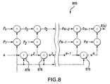
- FIG. 8 is a functional diagram of a polynomial function generator 800 , in accordance with polynomial function generators (i.e., polynomial function generators 430 , 432 , 434 in FIGS. 4 and 6 , and polynomial function generator 750 in FIG. 7 ) used in embodiments described herein.
- the input variable a passes through successive multipliers 876 to produce increasing powers of a (i.e., a, a 2 , a 3 . . . a N ⁇ 1 , a N ).
- the above described embodiments provide spatially efficient methods and apparatuses for implementing dewarping and/or perspection correction when processing an input image.
- the product, summing, and subtraction circuits in embodiments described herein may be implemented by a single arithmetic circuit or program, multiple circuits or programs, or through other known circuits or devices.
- the processing described may be implemented on a stand-alone image processor, as part of an imaging device, or as part of a system-on-chip device that contains image acquisitions and processing circuitry.
- the polynomial function generators in the embodiments described herein may be of any appropriate order for image processing. Accordingly, embodiments of the image processor and address mapping units are not limited to those described above.
- FIG. 9 illustrates a simplified block diagram of a system-on-chip semiconductor CMOS imaging device 900 having a pixel array 980 including a plurality of pixel cells arranged in a predetermined number of columns and rows. Each pixel cell is configured to receive incident photons and to convert the incident photons into electrical signals.
- Pixel cells of pixel array 980 are output row-by-row as activated by a row driver 981 in response to a row address decoder 982 .
- Column driver 984 and column address decoder 985 are also used to selectively activate individual pixel columns.
- An imager control circuit 983 controls address decoders 982 , 985 for selecting the appropriate row and column lines for pixel readout.
- the control circuit 983 also controls the row and column driver circuitry 981 , 984 such that driving voltages may be applied.
- the imager control circuit 983 triggers the pixel array 980 , via the row and column decoders 982 , 985 and row and column drivers 981 , 984 to capture frames of an image.
- each pixel cell For each frame captured, each pixel cell generally outputs both a pixel reset signal v rst and a pixel image signal v sig , which are read by a sample and hold circuit 986 according to a sampling scheme, for example, a correlated double sampling (“CDS”) scheme.
- the pixel reset signal v rst represents a reset state of a pixel cell.
- the pixel image signal v sig represents the amount of charge generated by the photosensor in the pixel cell in response to applied light during an integration period.
- the pixel reset and image signals v rst , v sig are sampled, held and amplified by the sample and hold circuit 986 .
- the sample and hold circuit 986 outputs amplified pixel reset and image signals V rst , V sig .
- the difference between V sig and V rst represents the actual pixel cell output with common-mode noise eliminated.
- the differential signal (e.g., V rst ⁇ V sig ) is produced by differential amplifier 987 for each readout pixel cell.
- the differential signals are digitized by an analog-to-digital (A/D) converter 988 .
- the analog-to-digital converter 988 supplies the digitized pixel signals f i (x,y) to image processor 300 , which receives and stores the pixel signals from the ADC 988 and performs dewarping and perspective correction, as described above.
- image processor 300 includes output address generator 320 , address mapping unit 322 , buffer 324 , and interpolation filter 326 .
- Image processor 300 outputs pixel signals f(x o , y o ) for storage in a memory, such as the random access memory 1094 ( FIG. 10 ).
- Embodiments of the methods and apparatuses described herein may be used in any system which employs a moving image or video imaging device, including, but not limited to a computer system, camera system, scanner, machine vision, vehicle navigation, video phone, surveillance system, auto focus system, star tracker system, motion detection system, image stabilization system, and other imaging systems.
- Example digital camera systems in which the invention may be used include video digital cameras, still cameras with video options, cell-phone cameras, handheld personal digital assistant (PDA) cameras, and other types of cameras.
- PDA personal digital assistant
- FIG. 10 shows a typical system 1000 in which an imaging device 900 implementing an embodiment of the image processor 300 described herein may be employed; in this example, a digital camera.
- the system 1000 includes an imaging device 900 that includes either software or hardware to implement the image processing in accordance with the embodiments described above.
- System 1000 also may include a processing unit 1093 , such as a microprocessor, that controls system functions and which communicates with an input/output (I/O) device 1096 over a bus 1092 .
- Imaging device 1000 also communicates with the processing unit 1093 over the bus 1092 .
- System 1000 also includes random access memory (RAM) 1094 , and can include removable storage memory 1095 , such as flash memory, which also communicates with the processing unit 1093 over the bus 1092 .
- Lens 1090 focuses an image on a pixel array of the imaging device 900 when shutter release button 1091 is pressed.
- CMOS imaging devices have broader applicability and may be used in any imaging apparatus which generates pixel output values, including charge-coupled devices CCDs and other imaging devices.
Landscapes
- Engineering & Computer Science (AREA)
- Physics & Mathematics (AREA)
- General Physics & Mathematics (AREA)
- Theoretical Computer Science (AREA)
- Multimedia (AREA)
- Signal Processing (AREA)
- Image Processing (AREA)
Abstract
Description
g(a)=P N a N +P N-1 a N−1 . . . +P 2 a 2 +P 1 a+P 0. Equation 1:
Claims (27)
Applications Claiming Priority (2)
| Application Number | Priority Date | Filing Date | Title |
|---|---|---|---|
| GB0813124A GB2461912A (en) | 2008-07-17 | 2008-07-17 | Method and apparatus for dewarping and/or perspective correction of an image |
| GB0813124.5 | 2008-07-17 |
Publications (2)
| Publication Number | Publication Date |
|---|---|
| US20100014770A1 US20100014770A1 (en) | 2010-01-21 |
| US8411998B2 true US8411998B2 (en) | 2013-04-02 |
Family
ID=39737225
Family Applications (1)
| Application Number | Title | Priority Date | Filing Date |
|---|---|---|---|
| US12/222,950 Active 2031-09-19 US8411998B2 (en) | 2008-07-17 | 2008-08-20 | Method and apparatus providing perspective correction and/or image dewarping |
Country Status (2)
| Country | Link |
|---|---|
| US (1) | US8411998B2 (en) |
| GB (1) | GB2461912A (en) |
Cited By (8)
| Publication number | Priority date | Publication date | Assignee | Title |
|---|---|---|---|---|
| US9085261B2 (en) | 2011-01-26 | 2015-07-21 | Magna Electronics Inc. | Rear vision system with trailer angle detection |
| US9446713B2 (en) | 2012-09-26 | 2016-09-20 | Magna Electronics Inc. | Trailer angle detection system |
| US9558409B2 (en) | 2012-09-26 | 2017-01-31 | Magna Electronics Inc. | Vehicle vision system with trailer angle detection |
| US9749554B2 (en) | 2015-08-20 | 2017-08-29 | Semiconductor Components Industries, Llc | Systems and methods for weighted image signal readout |
| US10002413B2 (en) | 2014-07-22 | 2018-06-19 | Hewlett-Packard Development Company, L.P. | Recovering planar projections |
| US10086870B2 (en) | 2015-08-18 | 2018-10-02 | Magna Electronics Inc. | Trailer parking assist system for vehicle |
| US10160382B2 (en) | 2014-02-04 | 2018-12-25 | Magna Electronics Inc. | Trailer backup assist system |
| US10331966B1 (en) * | 2018-10-19 | 2019-06-25 | Capital One Services, Llc | Image processing to detect a rectangular object |
Families Citing this family (17)
| Publication number | Priority date | Publication date | Assignee | Title |
|---|---|---|---|---|
| FR2942343B1 (en) * | 2009-02-16 | 2012-10-12 | Airbus France | AIRCRAFT EQUIPMENT ASSEMBLY COMPRISING A VIDEO SENSOR AND AT LEAST TWO HIGH HEAD VISUALIZATION DEVICES |
| GB2470740B (en) * | 2009-06-02 | 2015-04-22 | Aptina Imaging Corp | Systems and methods for the efficient computation of image transforms |
| US9495876B2 (en) | 2009-07-27 | 2016-11-15 | Magna Electronics Inc. | Vehicular camera with on-board microcontroller |
| JP5223811B2 (en) * | 2009-08-06 | 2013-06-26 | 株式会社日本自動車部品総合研究所 | Image correction apparatus, image correction method, and conversion map creation method used therefor |
| DE102010042248A1 (en) * | 2010-10-11 | 2012-04-12 | Robert Bosch Gmbh | Method and device for visualizing an environment of a vehicle |
| US9900522B2 (en) | 2010-12-01 | 2018-02-20 | Magna Electronics Inc. | System and method of establishing a multi-camera image using pixel remapping |
| US9185352B1 (en) | 2010-12-22 | 2015-11-10 | Thomas Jacques | Mobile eye tracking system |
| US8970589B2 (en) * | 2011-02-10 | 2015-03-03 | Edge 3 Technologies, Inc. | Near-touch interaction with a stereo camera grid structured tessellations |
| DE102011007644A1 (en) | 2011-04-19 | 2012-10-25 | Robert Bosch Gmbh | Method and device for determining values suitable for equalizing an image and for equalizing an image |
| US8548274B2 (en) * | 2011-04-29 | 2013-10-01 | Aptina Imaging Corporation | Systems and methods for efficient storage of image transformations |
| US9153007B2 (en) * | 2011-09-21 | 2015-10-06 | Semiconductor Components Industries, Llc | Imaging systems with conformal image buffers |
| US10755110B2 (en) | 2013-06-28 | 2020-08-25 | Magna Electronics Inc. | Trailering assist system for vehicle |
| AU2015252750B2 (en) * | 2014-04-29 | 2021-01-21 | Farrow Norris Pty Ltd | Method and system for comparative data analysis |
| DE102014212819A1 (en) * | 2014-07-02 | 2016-01-07 | Zf Friedrichshafen Ag | Location-dependent representation of vehicle environment data on a mobile unit |
| US10187590B2 (en) | 2015-10-27 | 2019-01-22 | Magna Electronics Inc. | Multi-camera vehicle vision system with image gap fill |
| US10152767B1 (en) * | 2016-12-15 | 2018-12-11 | The Mathworks, Inc. | Memory efficient on-chip buffering for projective transformation |
| US11796377B2 (en) * | 2020-06-24 | 2023-10-24 | Baker Hughes Holdings Llc | Remote contactless liquid container volumetry |
Citations (43)
| Publication number | Priority date | Publication date | Assignee | Title |
|---|---|---|---|---|
| US4841292A (en) * | 1986-08-11 | 1989-06-20 | Allied-Signal Inc. | Third dimension pop up generation from a two-dimensional transformed image display |
| US5870076A (en) * | 1994-11-11 | 1999-02-09 | Daewoo Electronics, Co., Ltd. | Pixel data correction apparatus for use with an actuated mirror array |
| US5903319A (en) * | 1991-05-13 | 1999-05-11 | Interactive Pictures Corporation | Method for eliminating temporal and spacial distortion from interlaced video signals |
| US6069668A (en) * | 1997-04-07 | 2000-05-30 | Pinnacle Systems, Inc. | System and method for producing video effects on live-action video |
| JP2000331151A (en) | 1999-05-25 | 2000-11-30 | Nec Corp | Image processing method, image distortion correction processor and storage medium recording program of the processor |
| US6236404B1 (en) | 1995-11-09 | 2001-05-22 | Hitachi, Ltd. | Perspective projection calculation devices and methods |
| US6346967B1 (en) | 1994-05-27 | 2002-02-12 | Be Here Corporation | Method apparatus and computer program products for performing perspective corrections to a distorted image |
| US20020180727A1 (en) | 2000-11-22 | 2002-12-05 | Guckenberger Ronald James | Shadow buffer control module method and software construct for adjusting per pixel raster images attributes to screen space and projector features for digital warp, intensity transforms, color matching, soft-edge blending, and filtering for multiple projectors and laser projectors |
| US20020191838A1 (en) * | 1999-12-29 | 2002-12-19 | Setterholm Jeffrey M. | Any aspect passive volumetric image processing method |
| EP1276074A2 (en) | 2001-07-09 | 2003-01-15 | Xerox Corporation | Method and apparatus for resolving perspective distortion in a document image and for calculating line sums in images |
| US20030043303A1 (en) | 2001-06-12 | 2003-03-06 | Bonaventure Karuta | System and method for correcting multiple axis displacement distortion |
| JP2004072553A (en) | 2002-08-08 | 2004-03-04 | Digital Zuu:Kk | Image distortion correction method, and program for the same |
| US6747702B1 (en) | 1998-12-23 | 2004-06-08 | Eastman Kodak Company | Apparatus and method for producing images without distortion and lateral color aberration |
| US20040156558A1 (en) | 2003-02-04 | 2004-08-12 | Kim Sang Yeon | Image warping method and apparatus thereof |
| JP2005018195A (en) | 2003-06-24 | 2005-01-20 | Minolta Co Ltd | Image processing apparatus and image processing program |
| US20050058360A1 (en) | 2003-09-12 | 2005-03-17 | Thomas Berkey | Imaging system and method for displaying and/or recording undistorted wide-angle image data |
| US20050083248A1 (en) | 2000-12-22 | 2005-04-21 | Frank Biocca | Mobile face capture and image processing system and method |
| US6885392B1 (en) | 1999-12-31 | 2005-04-26 | Stmicroelectronics, Inc. | Perspective correction for preview area of panoramic digital camera |
| US20050174437A1 (en) | 2004-02-10 | 2005-08-11 | Fujitsu Limited | Distortion correction circuit |
| US20050180655A1 (en) * | 2002-10-08 | 2005-08-18 | Akihiro Ohta | Image conversion device image conversion method and image projection device |
| JP2005234776A (en) | 2004-02-18 | 2005-09-02 | Oki Electric Ind Co Ltd | Processor for correcting image distortion and method therefor |
| US7002603B2 (en) | 2001-08-21 | 2006-02-21 | Sony United Kingdom Limited | Data processing apparatus and method of processing data |
| US20060050074A1 (en) | 2004-09-09 | 2006-03-09 | Silicon Optix Inc. | System and method for representing a general two dimensional spatial transformation |
| JP2006141005A (en) | 2004-11-01 | 2006-06-01 | Hewlett-Packard Development Co Lp | System and method for correcting image perspective |
| US7067808B2 (en) * | 2003-10-14 | 2006-06-27 | Topcon Corporation | Electron beam system and electron beam measuring and observing method |
| CA2498484A1 (en) | 2005-02-25 | 2006-08-25 | Symagery Microsystems Inc. | Automatic perspective detection and correction for document imaging |
| US7126616B2 (en) | 2001-06-12 | 2006-10-24 | Silicon Optix Inc. | Method and system for processing a non-linear two dimensional spatial transformation |
| US20060274972A1 (en) | 2001-08-28 | 2006-12-07 | Adobe Systems Incorporated | Methods and apparatus for shifting perspective in a composition image |
| JP2007028273A (en) | 2005-07-19 | 2007-02-01 | Realviz:Kk | Image distortion correcting method and program for the same |
| US7224392B2 (en) | 2002-01-17 | 2007-05-29 | Eastman Kodak Company | Electronic imaging system having a sensor for correcting perspective projection distortion |
| CN1996389A (en) | 2007-01-09 | 2007-07-11 | 北京航空航天大学 | Method for quickly correcting distortion of camera based on collinear feature point |
| US20070198586A1 (en) | 2006-02-22 | 2007-08-23 | Hardy Mark D | Methods and apparatus for providing a configurable geospatial data provisioning framework |
| US20070196004A9 (en) | 1992-01-21 | 2007-08-23 | Sri International, Inc. | Method and apparatus for transforming coordinate systems in a telemanipulation system |
| US20070206877A1 (en) | 2006-03-02 | 2007-09-06 | Minghui Wu | Model-based dewarping method and apparatus |
| US7268803B1 (en) | 1999-08-26 | 2007-09-11 | Ricoh Company, Ltd. | Image processing method and apparatus, digital camera, image processing system and computer readable medium |
| JP2007249967A (en) | 2006-03-10 | 2007-09-27 | Sony Taiwan Ltd | Perspective correction panning method for wide-angle image |
| US20070227026A1 (en) | 2006-02-14 | 2007-10-04 | Werner Krachtus | Method, system and scale for the determination and/or simulation of proportions |
| US20070268530A1 (en) | 2001-10-16 | 2007-11-22 | Gagliano Jeffrey A | Linear imager rescaling method |
| US20070273692A1 (en) | 2006-05-26 | 2007-11-29 | Samsung Electronics Co., Ltd | 3-Dimensional graphics processing method, medium and apparatus performing perspective correction |
| US20070280554A1 (en) | 2004-02-17 | 2007-12-06 | Corel Corporation | Method and apparatus for correction of perspective distortion |
| US20070285420A1 (en) | 2006-05-04 | 2007-12-13 | Brown Battle M | Systems and methods for photogrammetric rendering |
| US20080074415A1 (en) | 2006-08-24 | 2008-03-27 | Samsung Electronics Co., Ltd. | Method, medium and apparatus rendering 3D graphic data |
| US7532760B2 (en) * | 2002-08-27 | 2009-05-12 | Aptina Imaging Corporation | CMOS image sensor apparatus with on-chip real-time pipelined JPEG compression module |
-
2008
- 2008-07-17 GB GB0813124A patent/GB2461912A/en not_active Withdrawn
- 2008-08-20 US US12/222,950 patent/US8411998B2/en active Active
Patent Citations (44)
| Publication number | Priority date | Publication date | Assignee | Title |
|---|---|---|---|---|
| US4841292A (en) * | 1986-08-11 | 1989-06-20 | Allied-Signal Inc. | Third dimension pop up generation from a two-dimensional transformed image display |
| US5903319A (en) * | 1991-05-13 | 1999-05-11 | Interactive Pictures Corporation | Method for eliminating temporal and spacial distortion from interlaced video signals |
| US7333642B2 (en) | 1992-01-21 | 2008-02-19 | Sri International, Inc. | Method and apparatus for transforming coordinate systems in a telemanipulation system |
| US20070196004A9 (en) | 1992-01-21 | 2007-08-23 | Sri International, Inc. | Method and apparatus for transforming coordinate systems in a telemanipulation system |
| US6346967B1 (en) | 1994-05-27 | 2002-02-12 | Be Here Corporation | Method apparatus and computer program products for performing perspective corrections to a distorted image |
| US5870076A (en) * | 1994-11-11 | 1999-02-09 | Daewoo Electronics, Co., Ltd. | Pixel data correction apparatus for use with an actuated mirror array |
| US6236404B1 (en) | 1995-11-09 | 2001-05-22 | Hitachi, Ltd. | Perspective projection calculation devices and methods |
| US6069668A (en) * | 1997-04-07 | 2000-05-30 | Pinnacle Systems, Inc. | System and method for producing video effects on live-action video |
| US6747702B1 (en) | 1998-12-23 | 2004-06-08 | Eastman Kodak Company | Apparatus and method for producing images without distortion and lateral color aberration |
| JP2000331151A (en) | 1999-05-25 | 2000-11-30 | Nec Corp | Image processing method, image distortion correction processor and storage medium recording program of the processor |
| US7268803B1 (en) | 1999-08-26 | 2007-09-11 | Ricoh Company, Ltd. | Image processing method and apparatus, digital camera, image processing system and computer readable medium |
| US20020191838A1 (en) * | 1999-12-29 | 2002-12-19 | Setterholm Jeffrey M. | Any aspect passive volumetric image processing method |
| US6885392B1 (en) | 1999-12-31 | 2005-04-26 | Stmicroelectronics, Inc. | Perspective correction for preview area of panoramic digital camera |
| US20020180727A1 (en) | 2000-11-22 | 2002-12-05 | Guckenberger Ronald James | Shadow buffer control module method and software construct for adjusting per pixel raster images attributes to screen space and projector features for digital warp, intensity transforms, color matching, soft-edge blending, and filtering for multiple projectors and laser projectors |
| US20050083248A1 (en) | 2000-12-22 | 2005-04-21 | Frank Biocca | Mobile face capture and image processing system and method |
| US20030043303A1 (en) | 2001-06-12 | 2003-03-06 | Bonaventure Karuta | System and method for correcting multiple axis displacement distortion |
| US7126616B2 (en) | 2001-06-12 | 2006-10-24 | Silicon Optix Inc. | Method and system for processing a non-linear two dimensional spatial transformation |
| EP1276074A2 (en) | 2001-07-09 | 2003-01-15 | Xerox Corporation | Method and apparatus for resolving perspective distortion in a document image and for calculating line sums in images |
| US7002603B2 (en) | 2001-08-21 | 2006-02-21 | Sony United Kingdom Limited | Data processing apparatus and method of processing data |
| US20060274972A1 (en) | 2001-08-28 | 2006-12-07 | Adobe Systems Incorporated | Methods and apparatus for shifting perspective in a composition image |
| US20070268530A1 (en) | 2001-10-16 | 2007-11-22 | Gagliano Jeffrey A | Linear imager rescaling method |
| US7224392B2 (en) | 2002-01-17 | 2007-05-29 | Eastman Kodak Company | Electronic imaging system having a sensor for correcting perspective projection distortion |
| JP2004072553A (en) | 2002-08-08 | 2004-03-04 | Digital Zuu:Kk | Image distortion correction method, and program for the same |
| US7532760B2 (en) * | 2002-08-27 | 2009-05-12 | Aptina Imaging Corporation | CMOS image sensor apparatus with on-chip real-time pipelined JPEG compression module |
| US20050180655A1 (en) * | 2002-10-08 | 2005-08-18 | Akihiro Ohta | Image conversion device image conversion method and image projection device |
| US20040156558A1 (en) | 2003-02-04 | 2004-08-12 | Kim Sang Yeon | Image warping method and apparatus thereof |
| JP2005018195A (en) | 2003-06-24 | 2005-01-20 | Minolta Co Ltd | Image processing apparatus and image processing program |
| US20050058360A1 (en) | 2003-09-12 | 2005-03-17 | Thomas Berkey | Imaging system and method for displaying and/or recording undistorted wide-angle image data |
| US7067808B2 (en) * | 2003-10-14 | 2006-06-27 | Topcon Corporation | Electron beam system and electron beam measuring and observing method |
| US20050174437A1 (en) | 2004-02-10 | 2005-08-11 | Fujitsu Limited | Distortion correction circuit |
| US20070280554A1 (en) | 2004-02-17 | 2007-12-06 | Corel Corporation | Method and apparatus for correction of perspective distortion |
| JP2005234776A (en) | 2004-02-18 | 2005-09-02 | Oki Electric Ind Co Ltd | Processor for correcting image distortion and method therefor |
| US20060050074A1 (en) | 2004-09-09 | 2006-03-09 | Silicon Optix Inc. | System and method for representing a general two dimensional spatial transformation |
| JP2006141005A (en) | 2004-11-01 | 2006-06-01 | Hewlett-Packard Development Co Lp | System and method for correcting image perspective |
| CA2498484A1 (en) | 2005-02-25 | 2006-08-25 | Symagery Microsystems Inc. | Automatic perspective detection and correction for document imaging |
| JP2007028273A (en) | 2005-07-19 | 2007-02-01 | Realviz:Kk | Image distortion correcting method and program for the same |
| US20070227026A1 (en) | 2006-02-14 | 2007-10-04 | Werner Krachtus | Method, system and scale for the determination and/or simulation of proportions |
| US20070198586A1 (en) | 2006-02-22 | 2007-08-23 | Hardy Mark D | Methods and apparatus for providing a configurable geospatial data provisioning framework |
| US20070206877A1 (en) | 2006-03-02 | 2007-09-06 | Minghui Wu | Model-based dewarping method and apparatus |
| JP2007249967A (en) | 2006-03-10 | 2007-09-27 | Sony Taiwan Ltd | Perspective correction panning method for wide-angle image |
| US20070285420A1 (en) | 2006-05-04 | 2007-12-13 | Brown Battle M | Systems and methods for photogrammetric rendering |
| US20070273692A1 (en) | 2006-05-26 | 2007-11-29 | Samsung Electronics Co., Ltd | 3-Dimensional graphics processing method, medium and apparatus performing perspective correction |
| US20080074415A1 (en) | 2006-08-24 | 2008-03-27 | Samsung Electronics Co., Ltd. | Method, medium and apparatus rendering 3D graphic data |
| CN1996389A (en) | 2007-01-09 | 2007-07-11 | 北京航空航天大学 | Method for quickly correcting distortion of camera based on collinear feature point |
Non-Patent Citations (8)
| Title |
|---|
| Dasu, A. et al., "A Survey of Media Processing Approaches", IEEE Transactions on Circuits and Systems for Video Technology, vol. 12, Issue 8; pp. 633-645, Aug. 2002. |
| Kang, S. B. et al., "High Dynamic Range Video", Interactive Visual Media Group, Microsoft Research, Redmond, WA. |
| Krutz, A. et al., "Improved Image Registration Using the Up-Sampled Domain", Communications Systems Group, TU Berlin, Berlin, Germany, School of IT and EE, Australian Defence Force Academy, Canberra, Australia. |
| Kunter, M. et al., "Optimal Multiple Sprite Generation Based on Physical Camera Parameter Estimation", Commun. Systems Group, Technische Universitatt berlin, Berlin, Germany, Dept. of Electrical & Computer Engineering, university of Alberta, Edmonton, Canada. |
| Li et al. ("Robust distortion correction of endoscope," SPIE vol. 6918, Feb. 2008, pp. 1-8). * |
| Li, X., "Vidoe Processing Via Implicit and Mixture Motion Models", IEEE Transactions on Circuits and Systems for Video Technology, vol. 17, Issue 8, pp. 953-963, Aug. 2007. |
| McCall, J. et al., "Video Based Lane Estimation and Tracking for Driver Assistance: Survey, Sytem, and Evaluation", IEEE Transactions on Intelligent Transporation Systems, Dec. 2004, Revised Jul. 2005. |
| Xu et al. ("Method for calibrating cameras with large lens distortion," Optical Engineering 45(4), Apr. 2006, pp. 1-8). * |
Cited By (30)
| Publication number | Priority date | Publication date | Assignee | Title |
|---|---|---|---|---|
| US9950738B2 (en) | 2011-01-26 | 2018-04-24 | Magna Electronics Inc. | Trailering assist system with trailer angle detection |
| US11820424B2 (en) | 2011-01-26 | 2023-11-21 | Magna Electronics Inc. | Trailering assist system with trailer angle detection |
| US9085261B2 (en) | 2011-01-26 | 2015-07-21 | Magna Electronics Inc. | Rear vision system with trailer angle detection |
| US10858042B2 (en) | 2011-01-26 | 2020-12-08 | Magna Electronics Inc. | Trailering assist system with trailer angle detection |
| US11410431B2 (en) | 2012-09-26 | 2022-08-09 | Magna Electronics Inc. | Vehicular control system with trailering assist function |
| US10300855B2 (en) | 2012-09-26 | 2019-05-28 | Magna Electronics Inc. | Trailer driving assist system |
| US9779313B2 (en) | 2012-09-26 | 2017-10-03 | Magna Electronics Inc. | Vehicle vision system with trailer angle detection |
| US10909393B2 (en) | 2012-09-26 | 2021-02-02 | Magna Electronics Inc. | Vehicular control system with trailering assist function |
| US10089541B2 (en) | 2012-09-26 | 2018-10-02 | Magna Electronics Inc. | Vehicular control system with trailering assist function |
| US11872939B2 (en) | 2012-09-26 | 2024-01-16 | Magna Electronics Inc. | Vehicular trailer angle detection system |
| US9802542B2 (en) | 2012-09-26 | 2017-10-31 | Magna Electronics Inc. | Trailer angle detection system calibration |
| US11285875B2 (en) | 2012-09-26 | 2022-03-29 | Magna Electronics Inc. | Method for dynamically calibrating a vehicular trailer angle detection system |
| US9446713B2 (en) | 2012-09-26 | 2016-09-20 | Magna Electronics Inc. | Trailer angle detection system |
| US9558409B2 (en) | 2012-09-26 | 2017-01-31 | Magna Electronics Inc. | Vehicle vision system with trailer angle detection |
| US10586119B2 (en) | 2012-09-26 | 2020-03-10 | Magna Electronics Inc. | Vehicular control system with trailering assist function |
| US10800332B2 (en) | 2012-09-26 | 2020-10-13 | Magna Electronics Inc. | Trailer driving assist system |
| US10493917B2 (en) | 2014-02-04 | 2019-12-03 | Magna Electronics Inc. | Vehicular trailer backup assist system |
| US10160382B2 (en) | 2014-02-04 | 2018-12-25 | Magna Electronics Inc. | Trailer backup assist system |
| US10002413B2 (en) | 2014-07-22 | 2018-06-19 | Hewlett-Packard Development Company, L.P. | Recovering planar projections |
| US10870449B2 (en) | 2015-08-18 | 2020-12-22 | Magna Electronics Inc. | Vehicular trailering system |
| US11673605B2 (en) | 2015-08-18 | 2023-06-13 | Magna Electronics Inc. | Vehicular driving assist system |
| US10086870B2 (en) | 2015-08-18 | 2018-10-02 | Magna Electronics Inc. | Trailer parking assist system for vehicle |
| US9749554B2 (en) | 2015-08-20 | 2017-08-29 | Semiconductor Components Industries, Llc | Systems and methods for weighted image signal readout |
| US10943140B2 (en) | 2018-10-19 | 2021-03-09 | Capital One Services, Llc | Image processing to detect a rectangular object |
| US11423633B2 (en) | 2018-10-19 | 2022-08-23 | Capital One Services, Llc | Image processing to detect a rectangular object |
| US20220392184A1 (en) * | 2018-10-19 | 2022-12-08 | Capital One Services, Llc | Image processing to detect a rectangular object |
| US11682225B2 (en) * | 2018-10-19 | 2023-06-20 | Capital One Services, Llc | Image processing to detect a rectangular object |
| US20230298375A1 (en) * | 2018-10-19 | 2023-09-21 | Capital One Services, Llc | Image processing to detect a rectangular object |
| US10331966B1 (en) * | 2018-10-19 | 2019-06-25 | Capital One Services, Llc | Image processing to detect a rectangular object |
| US12051258B2 (en) * | 2018-10-19 | 2024-07-30 | Capital One Services, Llc | Image processing to detect a rectangular object |
Also Published As
| Publication number | Publication date |
|---|---|
| GB2461912A (en) | 2010-01-20 |
| GB0813124D0 (en) | 2008-08-27 |
| US20100014770A1 (en) | 2010-01-21 |
Similar Documents
| Publication | Publication Date | Title |
|---|---|---|
| US8411998B2 (en) | Method and apparatus providing perspective correction and/or image dewarping | |
| US8934035B2 (en) | Correction of non-uniform sensitivity in an image array | |
| US9230306B2 (en) | System for reducing depth of field with digital image processing | |
| JP5746521B2 (en) | IMAGING DEVICE, ITS CONTROL METHOD, PROGRAM, AND STORAGE MEDIUM | |
| JP6372983B2 (en) | FOCUS DETECTION DEVICE, ITS CONTROL METHOD, AND IMAGING DEVICE | |
| WO2008027211A2 (en) | Method and apparatus for image noise reduction using noise models | |
| CN100454984C (en) | Signal processing device and signal processing method for solid-state imaging element | |
| CN107306335B (en) | Camera device and control method thereof | |
| US20080278613A1 (en) | Methods, apparatuses and systems providing pixel value adjustment for images produced with varying focal length lenses | |
| JP6525539B2 (en) | Imaging device and imaging device | |
| GB2442050A (en) | Image pixel value correction | |
| JP4363308B2 (en) | Signal processing apparatus and method for solid-state imaging device, and imaging apparatus | |
| US20110037882A1 (en) | Solid-state imaging device, method of driving solid-state imaging device, and electronic apparatus | |
| JP2016058877A (en) | Imaging apparatus and control method thereof | |
| JP2009049609A (en) | Correction circuit, correction method, and imaging apparatus | |
| JP2009077047A (en) | Electronic camera | |
| JP6566654B2 (en) | Control device, imaging device, control method, program, and storage medium | |
| US9967452B2 (en) | Imaging apparatus and imaging method for controlling auto-focus | |
| JP6573379B2 (en) | Image processing apparatus, imaging apparatus, and image processing program | |
| JP6700751B2 (en) | IMAGING DEVICE, IMAGING DEVICE CONTROL METHOD, AND PROGRAM | |
| JP2006135425A (en) | Signal processor and processing method of solid state image sensor and imaging apparatus | |
| JP6728005B2 (en) | Imaging device, imaging method, and program | |
| JP4802423B2 (en) | Image shake correction apparatus and method, and imaging apparatus | |
| JP6590055B2 (en) | Imaging device | |
| JP6207173B2 (en) | Signal processing apparatus, control method thereof, and control program |
Legal Events
| Date | Code | Title | Description |
|---|---|---|---|
| AS | Assignment |
Owner name: MICRON TECHNOLOGY, INC.,IDAHO Free format text: ASSIGNMENT OF ASSIGNORS INTEREST;ASSIGNORS:HUGGETT, ANTHONY;KIRSCH, GRAHAM;REEL/FRAME:021473/0461 Effective date: 20080813 Owner name: MICRON TECHNOLOGY, INC., IDAHO Free format text: ASSIGNMENT OF ASSIGNORS INTEREST;ASSIGNORS:HUGGETT, ANTHONY;KIRSCH, GRAHAM;REEL/FRAME:021473/0461 Effective date: 20080813 |
|
| AS | Assignment |
Owner name: APTINA IMAGING CORPORATION,CAYMAN ISLANDS Free format text: ASSIGNMENT OF ASSIGNORS INTEREST;ASSIGNOR:MICRON TECHNOLOGY, INC.;REEL/FRAME:023245/0186 Effective date: 20080926 Owner name: APTINA IMAGING CORPORATION, CAYMAN ISLANDS Free format text: ASSIGNMENT OF ASSIGNORS INTEREST;ASSIGNOR:MICRON TECHNOLOGY, INC.;REEL/FRAME:023245/0186 Effective date: 20080926 |
|
| FEPP | Fee payment procedure |
Free format text: PAYOR NUMBER ASSIGNED (ORIGINAL EVENT CODE: ASPN); ENTITY STATUS OF PATENT OWNER: LARGE ENTITY |
|
| STCF | Information on status: patent grant |
Free format text: PATENTED CASE |
|
| FPAY | Fee payment |
Year of fee payment: 4 |
|
| MAFP | Maintenance fee payment |
Free format text: PAYMENT OF MAINTENANCE FEE, 8TH YEAR, LARGE ENTITY (ORIGINAL EVENT CODE: M1552); ENTITY STATUS OF PATENT OWNER: LARGE ENTITY Year of fee payment: 8 |
|
| MAFP | Maintenance fee payment |
Free format text: PAYMENT OF MAINTENANCE FEE, 12TH YEAR, LARGE ENTITY (ORIGINAL EVENT CODE: M1553); ENTITY STATUS OF PATENT OWNER: LARGE ENTITY Year of fee payment: 12 |