US8384103B2 - Increasing contrast in electronic color displays via surface texturing of LEDs - Google Patents
Increasing contrast in electronic color displays via surface texturing of LEDs Download PDFInfo
- Publication number
- US8384103B2 US8384103B2 US12/717,759 US71775910A US8384103B2 US 8384103 B2 US8384103 B2 US 8384103B2 US 71775910 A US71775910 A US 71775910A US 8384103 B2 US8384103 B2 US 8384103B2
- Authority
- US
- United States
- Prior art keywords
- led
- light
- discrete
- color display
- leds
- Prior art date
- Legal status (The legal status is an assumption and is not a legal conclusion. Google has not performed a legal analysis and makes no representation as to the accuracy of the status listed.)
- Active, expires
Links
- 239000004065 semiconductor Substances 0.000 claims abstract description 37
- 239000008393 encapsulating agent Substances 0.000 claims abstract description 22
- 230000005670 electromagnetic radiation Effects 0.000 claims description 7
- 230000001413 cellular effect Effects 0.000 claims 1
- 238000000034 method Methods 0.000 description 7
- 238000009792 diffusion process Methods 0.000 description 6
- 241000272168 Laridae Species 0.000 description 4
- 239000000463 material Substances 0.000 description 3
- 239000004593 Epoxy Substances 0.000 description 2
- 238000003486 chemical etching Methods 0.000 description 2
- 239000011521 glass Substances 0.000 description 2
- 238000003754 machining Methods 0.000 description 2
- 238000012986 modification Methods 0.000 description 2
- 230000004048 modification Effects 0.000 description 2
- 229920001296 polysiloxane Polymers 0.000 description 2
- 230000008878 coupling Effects 0.000 description 1
- 238000010168 coupling process Methods 0.000 description 1
- 238000005859 coupling reaction Methods 0.000 description 1
- 230000000694 effects Effects 0.000 description 1
- 238000005401 electroluminescence Methods 0.000 description 1
- 229910052736 halogen Inorganic materials 0.000 description 1
- 150000002367 halogens Chemical class 0.000 description 1
- 238000003384 imaging method Methods 0.000 description 1
Images


Classifications
-
- H—ELECTRICITY
- H10—SEMICONDUCTOR DEVICES; ELECTRIC SOLID-STATE DEVICES NOT OTHERWISE PROVIDED FOR
- H10H—INORGANIC LIGHT-EMITTING SEMICONDUCTOR DEVICES HAVING POTENTIAL BARRIERS
- H10H20/00—Individual inorganic light-emitting semiconductor devices having potential barriers, e.g. light-emitting diodes [LED]
- H10H20/80—Constructional details
- H10H20/84—Coatings, e.g. passivation layers or antireflective coatings
-
- H—ELECTRICITY
- H10—SEMICONDUCTOR DEVICES; ELECTRIC SOLID-STATE DEVICES NOT OTHERWISE PROVIDED FOR
- H10H—INORGANIC LIGHT-EMITTING SEMICONDUCTOR DEVICES HAVING POTENTIAL BARRIERS
- H10H20/00—Individual inorganic light-emitting semiconductor devices having potential barriers, e.g. light-emitting diodes [LED]
- H10H20/80—Constructional details
- H10H20/85—Packages
- H10H20/852—Encapsulations
- H10H20/853—Encapsulations characterised by their shape
-
- H—ELECTRICITY
- H01—ELECTRIC ELEMENTS
- H01L—SEMICONDUCTOR DEVICES NOT COVERED BY CLASS H10
- H01L2224/00—Indexing scheme for arrangements for connecting or disconnecting semiconductor or solid-state bodies and methods related thereto as covered by H01L24/00
- H01L2224/01—Means for bonding being attached to, or being formed on, the surface to be connected, e.g. chip-to-package, die-attach, "first-level" interconnects; Manufacturing methods related thereto
- H01L2224/42—Wire connectors; Manufacturing methods related thereto
- H01L2224/47—Structure, shape, material or disposition of the wire connectors after the connecting process
- H01L2224/48—Structure, shape, material or disposition of the wire connectors after the connecting process of an individual wire connector
- H01L2224/4805—Shape
- H01L2224/4809—Loop shape
- H01L2224/48091—Arched
-
- H—ELECTRICITY
- H01—ELECTRIC ELEMENTS
- H01L—SEMICONDUCTOR DEVICES NOT COVERED BY CLASS H10
- H01L2224/00—Indexing scheme for arrangements for connecting or disconnecting semiconductor or solid-state bodies and methods related thereto as covered by H01L24/00
- H01L2224/01—Means for bonding being attached to, or being formed on, the surface to be connected, e.g. chip-to-package, die-attach, "first-level" interconnects; Manufacturing methods related thereto
- H01L2224/42—Wire connectors; Manufacturing methods related thereto
- H01L2224/47—Structure, shape, material or disposition of the wire connectors after the connecting process
- H01L2224/48—Structure, shape, material or disposition of the wire connectors after the connecting process of an individual wire connector
- H01L2224/481—Disposition
- H01L2224/48151—Connecting between a semiconductor or solid-state body and an item not being a semiconductor or solid-state body, e.g. chip-to-substrate, chip-to-passive
- H01L2224/48221—Connecting between a semiconductor or solid-state body and an item not being a semiconductor or solid-state body, e.g. chip-to-substrate, chip-to-passive the body and the item being stacked
- H01L2224/48245—Connecting between a semiconductor or solid-state body and an item not being a semiconductor or solid-state body, e.g. chip-to-substrate, chip-to-passive the body and the item being stacked the item being metallic
- H01L2224/48247—Connecting between a semiconductor or solid-state body and an item not being a semiconductor or solid-state body, e.g. chip-to-substrate, chip-to-passive the body and the item being stacked the item being metallic connecting the wire to a bond pad of the item
-
- H—ELECTRICITY
- H01—ELECTRIC ELEMENTS
- H01L—SEMICONDUCTOR DEVICES NOT COVERED BY CLASS H10
- H01L2224/00—Indexing scheme for arrangements for connecting or disconnecting semiconductor or solid-state bodies and methods related thereto as covered by H01L24/00
- H01L2224/73—Means for bonding being of different types provided for in two or more of groups H01L2224/10, H01L2224/18, H01L2224/26, H01L2224/34, H01L2224/42, H01L2224/50, H01L2224/63, H01L2224/71
- H01L2224/732—Location after the connecting process
- H01L2224/73251—Location after the connecting process on different surfaces
- H01L2224/73265—Layer and wire connectors
-
- H—ELECTRICITY
- H01—ELECTRIC ELEMENTS
- H01L—SEMICONDUCTOR DEVICES NOT COVERED BY CLASS H10
- H01L2924/00—Indexing scheme for arrangements or methods for connecting or disconnecting semiconductor or solid-state bodies as covered by H01L24/00
-
- H—ELECTRICITY
- H01—ELECTRIC ELEMENTS
- H01L—SEMICONDUCTOR DEVICES NOT COVERED BY CLASS H10
- H01L2924/00—Indexing scheme for arrangements or methods for connecting or disconnecting semiconductor or solid-state bodies as covered by H01L24/00
- H01L2924/0001—Technical content checked by a classifier
- H01L2924/00012—Relevant to the scope of the group, the symbol of which is combined with the symbol of this group
-
- H—ELECTRICITY
- H01—ELECTRIC ELEMENTS
- H01L—SEMICONDUCTOR DEVICES NOT COVERED BY CLASS H10
- H01L2924/00—Indexing scheme for arrangements or methods for connecting or disconnecting semiconductor or solid-state bodies as covered by H01L24/00
- H01L2924/0001—Technical content checked by a classifier
- H01L2924/00014—Technical content checked by a classifier the subject-matter covered by the group, the symbol of which is combined with the symbol of this group, being disclosed without further technical details
-
- H—ELECTRICITY
- H01—ELECTRIC ELEMENTS
- H01L—SEMICONDUCTOR DEVICES NOT COVERED BY CLASS H10
- H01L2924/00—Indexing scheme for arrangements or methods for connecting or disconnecting semiconductor or solid-state bodies as covered by H01L24/00
- H01L2924/15—Details of package parts other than the semiconductor or other solid state devices to be connected
- H01L2924/181—Encapsulation
-
- H—ELECTRICITY
- H10—SEMICONDUCTOR DEVICES; ELECTRIC SOLID-STATE DEVICES NOT OTHERWISE PROVIDED FOR
- H10H—INORGANIC LIGHT-EMITTING SEMICONDUCTOR DEVICES HAVING POTENTIAL BARRIERS
- H10H20/00—Individual inorganic light-emitting semiconductor devices having potential barriers, e.g. light-emitting diodes [LED]
- H10H20/80—Constructional details
- H10H20/882—Scattering means
Definitions
- a pixel In the area of digital imaging, a pixel (or picture element) is usually the smallest item of information in an image. Pixels are normally arranged in a two-dimensional gird and are often represented using dots or squares. Each pixel is a sample of an original image, where more samples typically provide more accurate representations of the original image. The intensity of each pixel is usually variable. In electronic color displays, such as flat-panel televisions, each pixel has typically three or four components. A three component pixel may have, for example, red, green and blue components. A four component pixel may have, for example, cyan, magenta, yellow and black components.
- Color components are usually LEDs (Light Emitting Diodes).
- LEDs are usually based semiconductor diode chips. When a semiconductor diode chip is forward biased, electrons recombine with holes and energy is released in the form of light. This effect is called electroluminescence. The color of the light is determined by the energy gap of the semiconductor diode chip.
- the semiconductor diode chip is usually small in area, often less than 1 mm 2 .
- a package that contains a semiconductor diode chip is usually larger than the semiconductor diode chip. For example, the diameter of a discrete packaged LED may be 4 or 5 mm.
- a FCD (full color display) board typically uses discrete color LEDs to form a pixel.
- a FCD board is usually a very large video screen such as those used in baseball stadiums, arena events, music events and large format advertising on the side of buildings. Because FCD boards are often used outdoors, sunlight reflected into an LED can reduce the contrast (the difference in brightness between one pixel and another pixel) of the display. For example, sunlight reflected into an “off” pixel can cause the “off” pixel to appear brighter than it would have with no sunlight reflected into the off pixel.
- FIG. 1 is an isometric view of an embodiment of electrical leads.
- FIG. 2 is a sectional view of an LED in accordance with an exemplary embodiment of the invention.
- FIG. 3 is an isometric view of an LED in accordance with an exemplary embodiment of the invention.
- FIG. 4 is a top sectional view of an LED in accordance with an exemplary embodiment of the invention.
- FIG. 5 is a sectional view of an LED in accordance with an exemplary embodiment of the invention illustrating reflection of external light without texturing of a portion of the encapsulant.
- FIG. 6 is a sectional view of an LED in accordance with an exemplary embodiment of the invention illustrating a path of electromagnetic radiation emitted from a semi-conductor chip.
- FIG. 7 is a side view of a surface with hill-and-valley texturing in accordance with an exemplary embodiment of the invention illustrating diffusion of external light.
- FIG. 8 is a sectional view of an LED in accordance with an exemplary embodiment of the invention illustrating diffusion of external light with texturing of portions of the outer surface of the encapsulant.
- FIG. 9 is a sectional view of an LED in accordance with an embodiment of the invention.
- FIG. 10 is an isometric view of an LED with texturing on a portion of the surface of the encapsulant in accordance with an embodiment of the invention.
- FIG. 11 is a sectional view of an LED with texturing on a portion of the surface of the encapsulant in accordance with an embodiment of the invention.
- FIG. 12A is a top view of an electronic display in accordance with an embodiment of the present disclosure.
- FIG. 12B is a top view of an electronic display in accordance with an embodiment of the present disclosure.
- the drawings and description disclose a light-emitting semiconductor chip, electrical leads for electrically coupling power to the light-emitting semiconductor chip and an encapsulant.
- the encapsulant completely encases the light-emitting semiconductor chip and partially encases the electrical leads.
- a portion of the outer surface of the encapsulant is textured in order to diffuse light from light sources other than the light-emitting semiconductor chip. Diffusing light from light sources other than the light-emitting semiconductor chip reduces the amount of light that is reflected into the area where light from the semiconductor chip is directed. As a result, a video display containing many light-emitting semiconductor chips will have better contrast.
- the surface of the area where light from the semiconductor chip is directed is substantially untextured to allow more direct light to leave the encapsulant.
- FIG. 1 is an isometric view of an embodiment of electrical leads.
- electrical lead 102 contains a “cup” 106 where a light-emitting semiconductor (not shown), for example an LED, may be physically and electrically connected.
- Electrical leads 104 and 108 together with wire bonds may be used to make electrical connections to the light-emitting semiconductor.
- gull wing leads are used.
- other electrical leads such as J leads, SOJ leads, reverse gull wing leads and straight cut leads may be used in embodiments of this invention.
- FIG. 2 is a sectional view of an LED 200 in accordance with an exemplary embodiment of the invention.
- a first electrical lead 102 is electrically and physically connected to a light-emitting semiconductor chip 202 .
- the light-emitting semiconductor chip 202 is an LED chip.
- the light-emitting semiconductor chip 202 may be a semiconductor laser or other semiconductors that emit electromagnetic radiation.
- the electromagnetic radiation emitted from the light-emitting semiconductor chip 202 includes visible light, ultra-violet light and infra-red light.
- the encapsulant 212 completely encases the LED 202 and partially encases electrical leads 102 , 104 (not shown) and 108 (not shown).
- the encapsulant 212 includes sections 204 , 206 and 208 . Each of these sections may be made of the same or different materials. These materials include, but are not limited to, epoxy, silicone and glass.
- FIG. 3 is an isometric view of an LED 200 in accordance with an exemplary embodiment of the invention.
- each section 204 , 206 and 208 of the encapsulant 212 has an outer surface.
- Outer surfaces 302 and 304 are part of section 204 .
- Outer surface 306 is part of section 206 and outer surface 308 is part of section 208 .
- outer surfaces 302 , 304 and 306 are textured in order to diffuse light from light sources other than the LED chip 202 . This will be explained in more detail later.
- FIG. 4 is a top sectional view of an LED 200 in accordance with an exemplary embodiment of the invention.
- wire bond 402 is electrically connected to electrical lead 104 and the LED chip 202 .
- the wire bond 404 is electrically connected to electrical lead 108 and the LED chip 202 .
- both electrical leads 104 and 108 are electrically connected to power supply voltage VDD.
- either 104 or 108 alone may be connected to power supply voltage VDD.
- GND of the power supply is connected to electrical lead 102 in this example.
- FIG. 6 is a sectional view of an LED 200 in accordance with an exemplary embodiment of the invention illustrating a path of electromagnetic radiation emitted from a light-emitting semiconductor chip.
- the light-emitting semiconductor chip is an LED chip 202 .
- the electromagnetic radiation 602 , 604 , 606 , 608 , and 610 emitted from the LED chip 202 leaves surface 308 .
- the surface 308 is substantially untextured to allow as much light as possible to leave surface 308 . If the surface was textured, some of the light from LED chip 202 would be diffused. As a result, the LED 200 would not be as bright as it would have been without a textured surface 308 .
- FIG. 5 is a sectional view of an LED 200 in accordance with an exemplary embodiment of the invention illustrating the reflection of external light without texturing of the encapsulant.
- external light 504 from a source other than LED chip 202 is reflected from an inner wall of the cup 106 of the electrical lead 102 back through section 208 . Because the external light 504 was not emitted from the LED chip 202 , the light leaving surface 308 is brighter than it would have been without the external light 504 . Because the light leaving surface 308 is brighter than it would have been without the external light 504 , contrast is reduced between this LED 200 and any other LEDs that may be a part of an electronic color display.
- external light 506 from a source other than LED chip 202 is reflected from a surface of the electrical lead 102 back through section 208 .
- external light 502 from a source other than LED chip 202 is reflected from an inner wall of the cup 106 of the electrical lead 102 back through section 208 .
- external light 508 from a source other than LED chip 202 is reflected from a surface of the electrical lead 102 back through section 208 .
- the combination of external light 502 , 504 , 506 and 508 reflected back through section 208 causes the light leaving surface 308 to be brighter than it would have been without the external light 504 . Because the light leaving surface 308 is brighter than it would have been without the external lights 502 , 504 , 506 , and 508 , contrast is reduced between this LED 200 and any other LEDs that may be a part of an electronic color display.
- Sources of external light include sunlight and artificial light (e.g. light from sources other than the sun).
- Sources of artificial light include incandescent light, halogen light, fluorescent light, gas discharge light and electrical arc light.
- FIG. 7 is a side view of a surface 704 with “hill-and-valley” texturing in accordance with an exemplary embodiment of the invention illustrating diffusion of external light.
- a surface 704 is textured 702 using one of several methods.
- the type of texture shown in FIG. 7 is often called hill-and-valley texturing.
- the distance D from a hill top and to the bottom of a valley is about 1 to 2 microns.
- Other distances may be used.
- One method for texturing a surface uses electro-discharge machining.
- Another method for texturing a surface uses chemical etching, however other methods may be used.
- directional light 706 and 708 striking the textured surface 702 is diffused. Diffused light reduces the intensity of directional light by scattering it in many directions as shown in FIG. 7 .
- FIG. 8 is a sectional view of an LED 200 in accordance with an exemplary embodiment of the invention illustrating diffusion of external light with texturing of portions of the outer surface of the encapsulant 212 .
- surfaces 302 , 304 and 306 are textured.
- Surface 308 is not textured to allow light from the LED chip 202 to pass through surface 308 with little diffusion.
- Surface texturing induces surface diffusivity, not volumetric diffusivity.
- external light 804 and 808 impinging on surface 306 is scattered reducing the amount of external light reflected through surface 308 .
- External light 802 impinging on surface 304 is scattered reducing the amount of external light reflected through surface 308 .
- External light 806 impinging on surface 302 is scattered reducing the amount of external light reflected through surface 308 . Because the amount of external light reflected through surface 308 is reduced, contrast between LED 200 and any other LEDs in an electronic color display is increased.
- three surfaces 302 , 304 and 306 were textured. However fewer surfaces could be textured with improvement in the contrast of an electronic color display.
- FIG. 9 is a sectional view of an LED 900 in accordance with an embodiment of the invention.
- an LED chip 906 is physically and electrically attached to an electrical lead 902 .
- a wire bond 908 is electrically attached to electrical lead 904 and LED chip 906 .
- an LED chip 906 is used, however other light-emitting semiconductor chips may be used as well.
- An encapsulant 910 completely covers the LED 906 and the wire bond 908 and partially covers the electrical leads 902 and 904 . In this embodiment, straight cut leads are used. However, other electrical leads such as J leads, SOJ leads, reverse gull wing leads and gull wing leads may be used in the embodiments of this invention.
- the encapsulant 910 in this example is made of epoxy but other materials may be used such as silicone or glass.
- the portion 912 of surface 916 is not substantially textured.
- most of external light 914 passes through portion 912 of surface 916 and is reflected off electrical lead 902 back through the top of LED 900 .
- the light 914 reflected through the top of LED 900 is external light, not light emitted from LED chip 906 , light leaving the top of the LED 900 is brighter than it would have been without the external light 914 .
- the light leaving the top of LED 900 is brighter than it would have been without the external light 914 , contrast is reduced between this LED 900 and any other LEDs that may be a part of an electronic color display.
- FIG. 10 is an isometric view of an LED 900 with texturing on a portion 912 of the surface 916 of the encapsulant 910 in accordance with an embodiment of the invention.
- a portion 912 of the surface 916 of the LED 900 is textured.
- Portions 918 and 920 of the surface 916 are not textured.
- One method for texturing a surface uses electro-discharge machining.
- Another method for texturing a surface uses chemical etching; however other methods may be used.
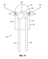
- FIG. 11 is a sectional view of an LED 900 with texturing on a portion 912 of the surface 916 of the encapsulant 910 in accordance with an embodiment of the invention.
- portion 912 of surface 916 is textured.
- Portions 918 and 920 of the surface 916 are not textured.
- Portion 918 is not textured to allow light from the LED chip 906 to pass through portion 918 with little diffusion.
- Surface texturing induces surface diffusivity, not volumetric diffusivity.
- portion 912 external light 1102 and 1104 impinging on portion 912 is scattered reducing the amount of external light reflected through portion 918 . Because the amount of external light 1102 and 1104 reflected through portion 918 is reduced, contrast between LED 900 and any other LEDs in an electronic display is increased. In this embodiment, only portion 912 was textured. However, more surfaces could be textured with improvement in the contrast of an electronic display.
- FIGS. 12A and 12B depict two possible configurations of an electronic display 1200 in accordance with embodiments of the present disclosure.
- an electronic display 1200 may be a color display and comprise a plurality of pixels 1202 , each of which may be provided with a plurality of LEDs.
- a pixel 1202 may comprise three discrete LEDs 1204 a , 1204 b , 1204 c .
- a pixel 1202 may comprise four discrete LEDs 1204 a , 1204 b , 1204 c , 1204 d.
Landscapes
- Led Device Packages (AREA)
- Illuminated Signs And Luminous Advertising (AREA)
Abstract
Description
Claims (9)
Priority Applications (2)
| Application Number | Priority Date | Filing Date | Title |
|---|---|---|---|
| US12/717,759 US8384103B2 (en) | 2010-03-04 | 2010-03-04 | Increasing contrast in electronic color displays via surface texturing of LEDs |
| TW100104468A TW201236216A (en) | 2010-03-04 | 2011-02-10 | Increasing contrast in electronic color displays via surface texturing of LEDs |
Applications Claiming Priority (1)
| Application Number | Priority Date | Filing Date | Title |
|---|---|---|---|
| US12/717,759 US8384103B2 (en) | 2010-03-04 | 2010-03-04 | Increasing contrast in electronic color displays via surface texturing of LEDs |
Publications (2)
| Publication Number | Publication Date |
|---|---|
| US20110215347A1 US20110215347A1 (en) | 2011-09-08 |
| US8384103B2 true US8384103B2 (en) | 2013-02-26 |
Family
ID=44530536
Family Applications (1)
| Application Number | Title | Priority Date | Filing Date |
|---|---|---|---|
| US12/717,759 Active 2030-11-30 US8384103B2 (en) | 2010-03-04 | 2010-03-04 | Increasing contrast in electronic color displays via surface texturing of LEDs |
Country Status (2)
| Country | Link |
|---|---|
| US (1) | US8384103B2 (en) |
| TW (1) | TW201236216A (en) |
Families Citing this family (4)
| Publication number | Priority date | Publication date | Assignee | Title |
|---|---|---|---|---|
| US11114594B2 (en) * | 2007-08-24 | 2021-09-07 | Creeled, Inc. | Light emitting device packages using light scattering particles of different size |
| US9287469B2 (en) * | 2008-05-02 | 2016-03-15 | Cree, Inc. | Encapsulation for phosphor-converted white light emitting diode |
| US8415692B2 (en) * | 2009-07-06 | 2013-04-09 | Cree, Inc. | LED packages with scattering particle regions |
| US10910532B2 (en) * | 2017-12-08 | 2021-02-02 | Advanced Semiconductor Engineering, Inc. | Semiconductor device package and method of manufacturing the same |
Citations (8)
| Publication number | Priority date | Publication date | Assignee | Title |
|---|---|---|---|---|
| US20050007000A1 (en) | 2000-11-02 | 2005-01-13 | 3M Innovative Properties Company | Brightness and contrast enhancement of direct view emissive displays |
| US20060290253A1 (en) | 2005-06-23 | 2006-12-28 | Fusion Optix, Inc. | Enhanced Diffusing Plates, Films and Backlights |
| US20070047254A1 (en) * | 2005-08-27 | 2007-03-01 | 3M Innovative Properties Company | Illumination assembly and system |
| US20070052663A1 (en) | 2005-09-05 | 2007-03-08 | Samsung Electronics Co., Ltd. | Liquid crystal display and method for lighting the same |
| US20080121918A1 (en) * | 2006-11-15 | 2008-05-29 | The Regents Of The University Of California | High light extraction efficiency sphere led |
| US20080308825A1 (en) * | 2007-06-14 | 2008-12-18 | Cree, Inc. | Encapsulant with scatterer to tailor spatial emission pattern and color uniformity in light emitting diodes |
| WO2008155368A1 (en) | 2007-06-18 | 2008-12-24 | Barco N.V. | Method and device for improving optical led performance |
| CN201285633Y (en) | 2008-10-30 | 2009-08-05 | 深圳市洲明科技有限公司 | LED display face mask |
-
2010
- 2010-03-04 US US12/717,759 patent/US8384103B2/en active Active
-
2011
- 2011-02-10 TW TW100104468A patent/TW201236216A/en unknown
Patent Citations (8)
| Publication number | Priority date | Publication date | Assignee | Title |
|---|---|---|---|---|
| US20050007000A1 (en) | 2000-11-02 | 2005-01-13 | 3M Innovative Properties Company | Brightness and contrast enhancement of direct view emissive displays |
| US20060290253A1 (en) | 2005-06-23 | 2006-12-28 | Fusion Optix, Inc. | Enhanced Diffusing Plates, Films and Backlights |
| US20070047254A1 (en) * | 2005-08-27 | 2007-03-01 | 3M Innovative Properties Company | Illumination assembly and system |
| US20070052663A1 (en) | 2005-09-05 | 2007-03-08 | Samsung Electronics Co., Ltd. | Liquid crystal display and method for lighting the same |
| US20080121918A1 (en) * | 2006-11-15 | 2008-05-29 | The Regents Of The University Of California | High light extraction efficiency sphere led |
| US20080308825A1 (en) * | 2007-06-14 | 2008-12-18 | Cree, Inc. | Encapsulant with scatterer to tailor spatial emission pattern and color uniformity in light emitting diodes |
| WO2008155368A1 (en) | 2007-06-18 | 2008-12-24 | Barco N.V. | Method and device for improving optical led performance |
| CN201285633Y (en) | 2008-10-30 | 2009-08-05 | 深圳市洲明科技有限公司 | LED display face mask |
Also Published As
| Publication number | Publication date |
|---|---|
| US20110215347A1 (en) | 2011-09-08 |
| TW201236216A (en) | 2012-09-01 |
Similar Documents
| Publication | Publication Date | Title |
|---|---|---|
| TWI531277B (en) | Lighting device, enclosure and method of lighting | |
| JP5624031B2 (en) | Solid-state lighting device with mixed light | |
| CN102714260B (en) | Solid state lighting device including light mixture | |
| TWI421446B (en) | Lighting device and lighting method | |
| US8115217B2 (en) | Systems and methods for packaging light-emitting diode devices | |
| TWI463636B (en) | High color rendering index illumination device with blue tones of increasing wavelength | |
| TWI452721B (en) | Method and device for manufacturing textured surface fluorescent layer | |
| EP2095438B1 (en) | Lighting device and lighting method | |
| US20060098440A1 (en) | Solid state lighting device with improved thermal management, improved power management, adjustable intensity, and interchangable lenses | |
| JP2009538532A (en) | Lighting device | |
| US9780274B2 (en) | Light-emitting apparatus and illumination apparatus | |
| TWM453969U (en) | Light emitting device | |
| US8384103B2 (en) | Increasing contrast in electronic color displays via surface texturing of LEDs | |
| US7659545B2 (en) | Illumination system | |
| Liu et al. | Analysis of factors affecting color distribution of white LEDs | |
| TWI464915B (en) | Coated diffuser cap for led illumination device | |
| US20160116141A1 (en) | Light-emitting device | |
| US11092311B2 (en) | Light extraction bridge in cups | |
| US20170077369A1 (en) | Light-emitting apparatus, illumination apparatus, and method of manufacturing light-emitting apparatus | |
| US20180301663A1 (en) | Optoelectronic package | |
| JP2010016108A (en) | Light-emitting device | |
| JP2017522734A (en) | LED light source for automotive applications | |
| US9831400B2 (en) | Light-emitting apparatus and illumination apparatus | |
| US20180287024A1 (en) | Semiconductor light-emitting module and semiconductor led chip thereof | |
| US20110089448A1 (en) | Single Encapsulant For A Plurality Of Light Sources |
Legal Events
| Date | Code | Title | Description |
|---|---|---|---|
| AS | Assignment |
Owner name: AVAGO TECHNOLOGIES ECBU IP (SINGAPORE) PTE. LTD., Free format text: ASSIGNMENT OF ASSIGNORS INTEREST;ASSIGNORS:WONG, KUM SOON;YONG, LIG YI;KEH, KEAN LOO;REEL/FRAME:024033/0452 Effective date: 20100301 |
|
| AS | Assignment |
Owner name: INTELLECTUAL DISCOVERY CO., LTD., KOREA, REPUBLIC Free format text: ASSIGNMENT OF ASSIGNORS INTEREST;ASSIGNORS:AVAGO TECHNOLOGIES GENERAL IP (SINGAPORE) PTE. LTD.;AVAGO TECHNOLOGIES ECBU IP (SINGAPORE) PTE. LTD.;AVAGO TECHNOLOGIES FIBER IP (SINGAPORE) PTE. LTD.;REEL/FRAME:028968/0296 Effective date: 20120709 |
|
| FEPP | Fee payment procedure |
Free format text: PAYOR NUMBER ASSIGNED (ORIGINAL EVENT CODE: ASPN); ENTITY STATUS OF PATENT OWNER: LARGE ENTITY |
|
| STCF | Information on status: patent grant |
Free format text: PATENTED CASE |
|
| FPAY | Fee payment |
Year of fee payment: 4 |
|
| AS | Assignment |
Owner name: BENCH WALK LIGHTING LLC, NEW YORK Free format text: ASSIGNMENT OF ASSIGNORS INTEREST;ASSIGNOR:INTELLECTUAL DISCOVERY CO., LTD.;REEL/FRAME:047308/0798 Effective date: 20180226 |
|
| MAFP | Maintenance fee payment |
Free format text: PAYMENT OF MAINTENANCE FEE, 8TH YEAR, LARGE ENTITY (ORIGINAL EVENT CODE: M1552); ENTITY STATUS OF PATENT OWNER: LARGE ENTITY Year of fee payment: 8 |
|
| FEPP | Fee payment procedure |
Free format text: MAINTENANCE FEE REMINDER MAILED (ORIGINAL EVENT CODE: REM.); ENTITY STATUS OF PATENT OWNER: LARGE ENTITY |