US8253502B2 - Spread spectrum clock generator and semiconductor device - Google Patents
Spread spectrum clock generator and semiconductor device Download PDFInfo
- Publication number
- US8253502B2 US8253502B2 US12/801,205 US80120510A US8253502B2 US 8253502 B2 US8253502 B2 US 8253502B2 US 80120510 A US80120510 A US 80120510A US 8253502 B2 US8253502 B2 US 8253502B2
- Authority
- US
- United States
- Prior art keywords
- voltage
- pass filter
- pulse signal
- low pass
- frequency
- Prior art date
- Legal status (The legal status is an assumption and is not a legal conclusion. Google has not performed a legal analysis and makes no representation as to the accuracy of the status listed.)
- Expired - Fee Related, expires
Links
- 238000001228 spectrum Methods 0.000 title claims abstract description 44
- 239000004065 semiconductor Substances 0.000 title claims description 25
- 238000001914 filtration Methods 0.000 claims abstract description 11
- 238000010586 diagram Methods 0.000 description 17
- 230000010355 oscillation Effects 0.000 description 12
- 230000000694 effects Effects 0.000 description 2
- 230000010354 integration Effects 0.000 description 2
- 238000012986 modification Methods 0.000 description 1
- 230000004048 modification Effects 0.000 description 1
- 230000001360 synchronised effect Effects 0.000 description 1
Images


Classifications
-
- H—ELECTRICITY
- H03—ELECTRONIC CIRCUITRY
- H03L—AUTOMATIC CONTROL, STARTING, SYNCHRONISATION OR STABILISATION OF GENERATORS OF ELECTRONIC OSCILLATIONS OR PULSES
- H03L7/00—Automatic control of frequency or phase; Synchronisation
- H03L7/06—Automatic control of frequency or phase; Synchronisation using a reference signal applied to a frequency- or phase-locked loop
- H03L7/16—Indirect frequency synthesis, i.e. generating a desired one of a number of predetermined frequencies using a frequency- or phase-locked loop
-
- H—ELECTRICITY
- H03—ELECTRONIC CIRCUITRY
- H03B—GENERATION OF OSCILLATIONS, DIRECTLY OR BY FREQUENCY-CHANGING, BY CIRCUITS EMPLOYING ACTIVE ELEMENTS WHICH OPERATE IN A NON-SWITCHING MANNER; GENERATION OF NOISE BY SUCH CIRCUITS
- H03B23/00—Generation of oscillations periodically swept over a predetermined frequency range
-
- H—ELECTRICITY
- H03—ELECTRONIC CIRCUITRY
- H03C—MODULATION
- H03C3/00—Angle modulation
- H03C3/02—Details
- H03C3/09—Modifications of modulator for regulating the mean frequency
- H03C3/0908—Modifications of modulator for regulating the mean frequency using a phase locked loop
- H03C3/095—Modifications of modulator for regulating the mean frequency using a phase locked loop applying frequency modulation to the loop in front of the voltage controlled oscillator
Definitions
- the present invention relates to a spread spectrum clock generator (SSCG), and in particular, to an SSCG spreading the spectrum of an operation clock used in a semiconductor device.
- SSCG spread spectrum clock generator
- LSI large-scale integration
- EMI electromagnetic interference
- An SSCG phase-locked loop (PLL) is often included in digital consumer devices such as printers and personal computers, as measures against EMI.
- PLL phase-locked loop
- an internal clock of an LSI circuit has a certain frequency, the spectrum exhibits a peak at a certain frequency, thereby causing radiated electromagnetic noise.
- By slightly changing such clock frequency with an SSCG energy of the spectrum can be distributed to other frequencies and the peak at such certain frequency can therefore be reduced.
- Patent Document 1 discloses a conventional SSCG
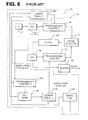
- FIG. 8 is a block diagram of a conventional SSCG disclosed in FIG. 6 of Patent Document 1.
- the clock generator of FIG. 8 includes programmable counters (or frequency dividers) 35 and 42 on the reference clock side and the feedback loop side, respectively.
- the clock generator changes the frequency of an operation clock by changing a frequency division ratio of the programmable counters 35 and 42 in the feedback loop in the PLL.
- the frequency division ratios of the programmable counters 35 and 42 are set by lookup tables 46 and 47 , respectively.
- VCO voltage-controlled oscillator
- FIG. 9 is a block diagram of another conventional SSCG disclosed in FIG. 7 of Patent Document 1.
- an analog modulation circuit 52 Based on this clock generator, an analog modulation circuit 52 generates a waveform for modulation, which is added to a control voltage applied to a second VCO 51 , to spread the spectrum of a clock outputted from the second VCO 51 .
- the analog modulation circuit 52 uses a triangular waveform generator and a log anti-log amplifier to generate the waveform for modulation.
- a phase detector 37 compares phases, and a filter 38 smoothes the comparison results.
- the modulation voltage generated by the analog modulation circuit 52 is added to the output from the filter 38 to supply the control voltage to the second VCO 51 .
- FIG. 10 is a block diagram of still another conventional SSCG disclosed in FIG. 8 of Patent Document 1.
- a reference clock oscillation circuit 72 including an LC circuit is used, and an oscillation frequency of the reference clock oscillation circuit 72 is directly modulated by the analog modulation circuit 52 .
- FIG. 11 is still another conventional SSCG disclosed in FIG. 9 of Patent Document 1.
- a read only memory (ROM) 82 and a digital-to-analog converter 83 are used to generate a modulation waveform.
- the modulation waveform is added to a control voltage outputted from the filter 38 to modulate an oscillation frequency of the second VCO 51 .
- the output from the filter 38 is added to the modulation voltage outputted from the digital-to-analog converter 83 .
- Patent Document 1 U.S. Pat. No. 5,488,627
- an SSCG which includes: a VCO generating an operation clock; a feedback control unit comparing a phase of the operation clock with a phase of a reference clock, and based on results of the comparison, generating a voltage used as a reference to oscillate the VCO; a modulated pulse generation unit generating a pulse signal obtained by performing a delta-sigma modulation on a component fluctuating a frequency of the operation clock; a level set unit setting an amplitude of the pulse signal; an adder adding a voltage generated by the feedback control unit and the pulse signal whose amplitude is set by the level set unit; and a low pass filter filtering a signal outputted from the adder and generating a control voltage applied to the VCO.
- an SSCG which includes: a VCO generating an operation clock; a feedback control unit comparing a phase of the operation clock with a phase of a reference clock, and based on results of the comparison, generating a voltage used as a reference to oscillate the VCO; a pulse generation unit generating a pulse signal; a level set unit setting an amplitude of the pulse signal; an adder adding a voltage generated by the feedback control unit and the pulse signal whose amplitude is set by the level set unit; and a low pass filter filtering a signal outputted from the adder and generating a control voltage applied to the voltage-controlled oscillator, wherein an oscillation frequency of the operation clock is fluctuated based on the pulse signal generated by the pulse generation unit.
- a semiconductor device which includes an SSCG and a clock synchronization circuit operating in synchronization with an operation clock.
- the SSCG includes: a VCO generating the operation clock, a feedback control unit comparing a phase of the operation clock with a phase of a reference clock, and based on results of the comparison, generating a voltage used as a reference to oscillate the VCO, a level set unit receiving a pulse signal obtained by performing a delta-sigma modulation on a component fluctuating a frequency of the operation clock and setting an amplitude of the pulse signal, an adder adding a voltage generated by the feedback control unit and the pulse signal whose amplitude is set by the level set unit, and a low pass filter filtering a signal outputted from the adder and generating a control voltage applied to the VCO.
- an SSCG that is less susceptible to circuit characteristic variation and that has arbitrary modulation characteristics can be obtained.
- FIG. 1 illustrates a block diagram of an SSCG according to example 1 of the present invention.
- FIG. 2A illustrates a voltage waveform obtained by integrating a voltage outputted from a charge pump circuit with a low pass filter when a PLL according to example 1 is locked.
- FIG. 2B illustrates a voltage waveform obtained by integrating a signal outputted from a level set unit with the low pass filter according to example 1.
- FIG. 2C illustrates a voltage waveform obtained by adding the voltage outputted from the charge pump circuit and the signal outputted from the level set unit with an adder and integrating the obtained signal with the low pass filter according to example 1.
- FIG. 3A schematically illustrates a relationship between a VCO control voltage and the frequency of an operation clock signal according to example 1.
- FIG. 3B illustrates a spread frequency spectrum and a non-spread frequency spectrum.
- FIG. 4 illustrates a block diagram of an SSCG according to example 2 of the present invention.
- FIG. 5 illustrates a block diagram of an SSCG according to example 3 of the present invention.
- FIG. 6 illustrates a block diagram of an SSCG according to example 4 of the present invention.
- FIG. 7 illustrates a block diagram of an SSCG according to example 5 of the present invention.
- FIG. 8 illustrates a block diagram of a conventional SSCG disclosed in FIG. 6 of Patent Document 1.
- FIG. 9 illustrates a block diagram of a conventional SSCG disclosed in FIG. 7 of Patent Document 1.
- FIG. 10 illustrates a block diagram of a conventional SSCG disclosed in FIG. 8 of Patent Document 1.
- FIG. 11 illustrates a block diagram of a conventional SSCG disclosed in FIG. 9 of Patent Document 1.
- an SSCG 1 of the present invention includes: a VCO 2 generating an operation clock Cko; a feedback control unit 3 comparing a phase of the operation clock Cko with a phase of a reference clock Ckr, and based on results of the comparison, generating a voltage used as a reference to oscillate the VCO 2 ; a modulated pulse generation unit ( 4 , 4 a ) generating a pulse signal obtained by performing a delta-sigma modulation on a component fluctuating a frequency of the operation clock Cko; a level set unit 5 setting an amplitude of the pulse signal; an adder 6 adding a voltage generated by the feedback control unit 3 and the pulse signal whose amplitude is set by the level set unit 5 ; and a low pass filter 7 filtering a signal outputted from the adder 6 and generating a control voltage applied to the VCO 2 .
- the low pass filter 7 demodulates the delta-sigma-modulated frequency change component into the control voltage to spread a spectrum, and the control voltage is applied to the VCO 2 .
- the circuit size can be reduced.
- a delta-sigma-modulated pulse is used, by using a digital circuit or the like, a clock generator having arbitrary frequency characteristics can be obtained relatively easily.
- the low pass filter 7 can be used to demodulate the delta-sigma-modulated signal and smooth the feedback control voltage. Further, it is preferable that the delta sigma modulation is performed depending on frequency characteristics of the low pass filter 7 .
- a desired pulse signal may be previously stored in the modulated pulse storage circuit 4 a .
- a hardware or software module may be used to carry out digital signal processing to generate a desired pulse signal.
- the modulated pulse generation unit 4 may be arranged outside a semiconductor chip including the VCO 2 .
- the level set unit 5 can set the level of frequency fluctuation.
- the pulse signal is obtained by performing a pulse density modulation on a component fluctuating a frequency of the operation clock.
- a delta-sigma modulation can be performed so that arbitrary frequency characteristics can be obtained by digital processing.
- An arbitrary signal may be used, as long as a desired frequency fluctuation component can be obtained after the low pass filter 7 performs integration and demodulation. Namely, an arbitrary signal may be used, as long as a desired frequency fluctuation component can be obtained after the signal passes through the low pass filter 7 .
- the SSCG includes, assuming that the low pass filter is a first low pass filter 7 , a second low pass filter 8 filtering a pulse signal whose amplitude is set by the level set unit 5 .
- the adder 6 adds a voltage generated by the feedback control unit 3 and a pulse signal filtered by the second low pass filter 8 .
- the delta-sigma-modulated frequency fluctuation component is demodulated by the second low pass filter 8 and the first low pass filter 7 .
- a semiconductor device includes the SSCG 1 and a clock synchronization circuit operating in synchronization with an operation clock, wherein the SSCG includes a VCO 2 generating the operation clock, a feedback control unit 3 comparing a phase of the operation clock Cko with a phase of a reference clock Ckr, and based on results of the comparison, generating a voltage used as a reference to oscillate the VCO 2 , a level set unit 5 receiving a pulse signal MP obtained by performing a delta-sigma modulation on a component fluctuating a frequency of the operation clock Cko and setting an amplitude of the pulse signal, an adder 6 adding a voltage generated by the feedback control unit 3 and the pulse signal whose amplitude is set by the level set unit 5 , and a low pass filter 7 filtering a signal outputted from the adder 6 and generating a control voltage applied to the VCO 2 .
- the SSCG includes a VCO 2 generating the operation clock, a feedback control unit 3 comparing a phase of the
- the operation clock generated by the clock generator 1 arranged in a semiconductor device is supplied as an operation clock in an internal circuit of the semiconductor device, and at least part of the internal circuit operates in synchronization with the operation clock.
- the delta-sigma-modulated pulse signal may be generated in the semiconductor device.
- a modulated pulse or modulated pulse data may be inputted from the outside. Examples of the present invention will be hereinafter described in detail with reference to the accompanying drawings.
- FIG. 1 illustrates a block diagram of an SSCG 1 according to example 1.
- a VCO 2 a feedback control unit 3 , and a low pass filter 7 form a general PLL circuit.
- the feedback control unit 3 includes a frequency phase comparator 3 a , a charge pump circuit 3 b , and a frequency divider 3 c .
- the frequency divider 3 c divides an operation clock Cko, and the obtained signal is compared with a reference clock Ckr by the frequency phase comparator 3 a .
- the frequency phase comparator 3 a compares the frequency or phase of these received signals, and based on results of the comparison, controls the charge pump circuit 3 b to output a pulse.
- the low pass filter 7 smoothes this pulse to generate a control voltage applied to the VCO 2 . Since the oscillation frequency of the VCO 2 is controlled by the control voltage, the operation clock Cko synchronizes with the reference clock Ckr and has a frequency higher by a multiple of a frequency division ratio of the frequency divider 3 c . Based on this PLL circuit formed by the VCO 2 , the feedback control unit 3 , and the low pass filter 7 , once the frequency phase of the reference clock Ckr and that of the operation clock Cko are synchronized with each other, the operation clock Cko stably oscillates at a certain frequency and is maintained unless setting conditions are changed from the outside.
- a modulated pulse generation unit 4 , a level set unit 5 , and an adder 6 are used to fluctuate the oscillation frequency of the operation clock Cko oscillating in the PLL circuit, so that the frequency spectrum is spread.
- the modulated pulse generation unit 4 generates a pulse signal MP, which is a signal obtained by performing a delta sigma modulation on a voltage component fluctuating the oscillation frequency in the PLL circuit.
- the pulse wave outputted as the pulse signal MP is demodulated by the low pass filter 7 into a voltage fluctuation of the control voltage applied to the VCO 2 . Then a frequency of the operation clock Cko is fluctuated.
- the level set unit 5 sets the amplitude of the pulse generated by the modulated pulse generation unit 4 .
- the magnitude of the fluctuation applied to the oscillation frequency of the operation clock Cko can be set.
- the adder 6 adds a voltage generated by the feedback control unit 3 (charge pump circuit 3 b ) and the pulse signal whose amplitude is set by the level set unit 5 .
- the low pass filter 7 smoothes the voltage signal generated by the addition carried out by the adder 6 , to generate the control voltage applied to the VCO 2 .
- FIG. 2A illustrates a voltage waveform obtained by integrating a voltage outputted from the charge pump circuit 3 b with the low pass filter 7 when the PLL is locked.
- the voltage from the level set unit 5 is 0, and the voltage outputted from the charge pump circuit 3 b is directly supplied to the low pass filter 7 .
- the PLL circuit formed by the VCO 2 , the feedback control unit 3 , and the low pass filter 7 is locked, the voltage outputted from the charge pump circuit 3 b is stable, and the low pass filter 7 outputs a certain fixed-level control voltage to the VCO 2 .
- FIG. 2B illustrates a voltage waveform obtained by integrating only a signal outputted from the level set unit 5 with the low pass filter 7 .
- the voltage waveform is indicated by a bold solid line, and the average of the voltage is indicated by a dashed line.
- the modulated pulse generation unit 4 outputs a delta-sigma-modulated pulse waveform, so that an ideal voltage waveform can be obtained when the low pass filter 7 integrates the signal with a predetermined time constant. Thus, after the pulse waveform is demodulated by passing through the low pass filter 7 , an ideal voltage waveform is obtained. While the voltage waveform illustrated in FIG.
- 2B is a simple triangular waveform, by changing the setting of the pulse outputted from the modulated pulse generation unit 4 , an arbitrary voltage waveform can be obtained. Further, while the voltage waveform is determined by the pulse waveform outputted from the modulated pulse generation unit 4 , the amplitude of the waveform is set by the level set unit 5 , and the amplitude of the voltage waveform outputted from the low pass filter 7 is accordingly determined.
- the pulse outputted from the modulated pulse generation unit 4 is a pulse density modulation (PDM) signal.
- PDM pulse density modulation
- FIG. 2C illustrates a voltage waveform obtained by adding the voltage outputted from the charge pump circuit 3 b and the signal outputted from the level set unit 5 with the adder 6 and integrating the obtained signal with the low pass filter 7 .
- the voltage waveform of FIG. 2A which is obtained by integrating the voltage outputted from the charge pump circuit 3 b with the low pass filter 7
- the voltage waveform of FIG. 2B which is obtained by integrating the voltage outputted from the level set unit 5 with the low pass filter 7
- the average of the voltage is equal to an average V 1 of the voltage outputted from the charge pump circuit 3 b .
- the average of the frequency remains the same as that obtained when modulation is not executed via the level set unit 5 .
- FIG. 3A schematically illustrates a relationship between the VCO control voltage and a frequency of the operation clock signal in example 1.
- the VCO control voltage is changed depending on the voltage outputted from the level set unit 5 , the oscillation frequency of the operation clock Cko outputted from the VCO 2 is accordingly changed.
- FIG. 3B illustrates profiles of a spread frequency spectrum and a non-spread frequency spectrum.
- a dashed line indicates a non-spread frequency spectrum and a solid line indicates a spread frequency spectrum. While the non-spread spectrum has a peak at a certain frequency, the spread spectrum has a suppressed and flattened peak.
- FIG. 4 illustrates a block diagram of an SSCG 1 according to example 2.
- elements substantially identical to those in FIG. 1 according to example 1 are denoted by the identical reference characters, and the descriptions thereof will be omitted.
- the modulated pulse generation unit 4 of FIG. 1 is replaced with a modulated pulse storage circuit 4 a .
- Other aspects of the SSCG 1 of FIG. 4 according to example 2 are the same as the SSCG 1 of FIG. 1 according to example 1.
- the modulated pulse storage circuit 4 a stores a modulated pulse prepared in advance. If the center frequency of the operation clock Cko and the frequency spectrum to be spread are determined in advance, a voltage waveform applied to the VCO 2 is determined so that the frequency spectrum can be obtained.
- the modulated pulse storage circuit 4 a can be realized by using a ROM. More specifically, an output pulse train may be stored in each address of a ROM, and the addresses may be sequentially updated to read the pulse train, so as to generate a desired modulated pulse train.
- a flash memory or a random access memory may be used as the modulated pulse storage circuit 4 a . If a flash memory or a RAM is used, even after a semiconductor device including the SSCG is manufactured, the modulated pulse can be changed.
- FIG. 5 is a block diagram illustrating an SSCG 1 according to example 3.
- the SSCG 1 illustrated in FIG. 5 further includes, assuming that the low pass filter 7 of example 1 is a first low pass filter 7 , a second low pass filter 8 that filters the pulse signal MP whose amplitude is set by the level set unit 5 .
- the adder 6 adds the voltage generated by the feedback control unit 3 and the pulse signal filtered by the second low pass filter 8 .
- FIG. 6 is a block diagram illustrating an SSCG 1 according to example 4.
- the SSCG 1 of FIG. 6 is a combination of the SSCGs according to examples 2 and 3. Namely, when FIG. 6 is compared with FIG. 1 (example 1), the modulated pulse storage circuit 4 a of example 2 is used as the modulated pulse generation unit 4 .
- the second low pass filter 8 is arranged between the level set unit 5 and the adder 6 .
- a delta-sigma-modulated pulse can be obtained easily, and frequency characteristics of the low pass filter 8 that demodulates the delta-sigma-modulated pulse signal and those of the low pass filter 7 that smoothes the signal outputted from the charge pump circuit 3 b can be made different.
- FIG. 7 is a block diagram illustrating an SSCG 1 particularly suitably used when formed on a semiconductor chip.
- the modulated pulse generation unit 4 of example 1 is not arranged on a semiconductor chip.
- a modulated pulse input unit 4 b is arranged so that a delta-sigma-modulated signal is supplied from the outside of the semiconductor chip.
- the SSCG 1 of FIG. 7 does not include the modulated pulse generation unit 4 , since the clock generator 1 can receive a delta-sigma-modulated pulse from the outside, the operation clock Cko having a spread spectrum can be obtained.
- the semiconductor device When the SSCG 1 is built in a semiconductor device, by supplying the operation clock Cko generated by the clock generator 1 to at least part of a circuit of the semiconductor device and synchronizing the circuit with the operation clock Cko, the semiconductor device can be operated. Further, needless to say, the SSCG 1 according to any one of examples 1 to 4, including the modulated pulse generation unit 4 or the modulated pulse storage circuit 4 a , may be arranged on a semiconductor chip.
- Mode 2 In the spread spectrum clock generator according to mode 1, wherein the pulse signal is obtained by performing a pulse density modulation on a component fluctuating a frequency of the operation clock.
- Mode 3 In the spread spectrum clock generator according to mode 1 or 2, further comprising, assuming that the low pass filter is a first low pass filter, a second low pass filter filtering a pulse signal whose amplitude is set by the level set unit, wherein the adder adds a voltage generated by the feedback control unit and a pulse signal filtered by the second low pass filter.
- Mode 4 In the spread spectrum clock generator according to any one of modes 1 to 3, wherein the modulated pulse generation unit comprises a storage circuit storing a previously generated pulse signal.
- Mode 5 A spread spectrum clock generator as set forth as the second aspect.
- Mode 6 In the spread spectrum clock generator according to mode 5, wherein the pulse generation unit generates a delta-sigma modulation pulse, said delta-sigma modulation pulse being demodulated by the low pass filter into a voltage fluctuation of the control voltage applied to the voltage-controlled oscillator.
- Mode 7) In the spread spectrum clock generator according to mode 5, wherein the pulse generation unit generates a pulse density modulation pulse, said pulse density modulation pulse being demodulated by the low pass filter into a voltage fluctuation of the control voltage applied to the voltage-controlled oscillator.
- Mode 8 In the spread spectrum clock generator according to any one of modes 5 to 7, further comprising, assuming that the low pass filter is a first low pass filter, a second low pass filter filtering a pulse signal whose amplitude is set by the level set unit, wherein the adder adds a voltage generated by the feedback control unit and a pulse signal filtered by the second low pass filter.
- Mode 9 In the spread spectrum clock generator according to any one of modes 5 to 8, wherein the pulse generation unit comprises a storage circuit storing a previously generated pulse signal.
- Mode 10) A semiconductor device as set forth as the third aspect.
- Mode 11 In the semiconductor device according to mode 10, further comprising a modulated pulse generation unit generating a pulse signal inputted to the level set unit.
- Mode 12 In the semiconductor device according to mode 11, wherein the modulated pulse generation unit comprises a storage circuit storing a previously generated pulse signal.
- Mode 13 In the semiconductor device according to any one of modes 10 to 12, further comprising, assuming that the low pass filter is a first low pass filter, a second low pass filter filtering a pulse signal whose amplitude is set by the level set unit, wherein the adder adds a voltage generated by the feedback control unit and a pulse signal filtered by the second low pass filter.
Landscapes
- Stabilization Of Oscillater, Synchronisation, Frequency Synthesizers (AREA)
- Manipulation Of Pulses (AREA)
Abstract
Description
(Mode 4): In the spread spectrum clock generator according to any one of
(Mode 5): A spread spectrum clock generator as set forth as the second aspect.
(Mode 6): In the spread spectrum clock generator according to
(Mode 7): In the spread spectrum clock generator according to
(Mode 8): In the spread spectrum clock generator according to any one of
(Mode 9): In the spread spectrum clock generator according to any one of
(Mode 10): A semiconductor device as set forth as the third aspect.
(Mode 11): In the semiconductor device according to mode 10, further comprising a modulated pulse generation unit generating a pulse signal inputted to the level set unit.
(Mode 12): In the semiconductor device according to mode 11, wherein the modulated pulse generation unit comprises a storage circuit storing a previously generated pulse signal.
(Mode 13): In the semiconductor device according to any one of modes 10 to 12, further comprising, assuming that the low pass filter is a first low pass filter, a second low pass filter filtering a pulse signal whose amplitude is set by the level set unit, wherein the adder adds a voltage generated by the feedback control unit and a pulse signal filtered by the second low pass filter.
Claims (20)
Applications Claiming Priority (2)
| Application Number | Priority Date | Filing Date | Title |
|---|---|---|---|
| JP2009-140235 | 2009-06-11 | ||
| JP2009140235A JP5190028B2 (en) | 2009-06-11 | 2009-06-11 | Spread spectrum clock generator |
Publications (2)
| Publication Number | Publication Date |
|---|---|
| US20100315172A1 US20100315172A1 (en) | 2010-12-16 |
| US8253502B2 true US8253502B2 (en) | 2012-08-28 |
Family
ID=43305919
Family Applications (1)
| Application Number | Title | Priority Date | Filing Date |
|---|---|---|---|
| US12/801,205 Expired - Fee Related US8253502B2 (en) | 2009-06-11 | 2010-05-27 | Spread spectrum clock generator and semiconductor device |
Country Status (2)
| Country | Link |
|---|---|
| US (1) | US8253502B2 (en) |
| JP (1) | JP5190028B2 (en) |
Cited By (2)
| Publication number | Priority date | Publication date | Assignee | Title |
|---|---|---|---|---|
| US11693446B2 (en) | 2021-10-20 | 2023-07-04 | International Business Machines Corporation | On-chip spread spectrum synchronization between spread spectrum sources |
| US11714127B2 (en) | 2018-06-12 | 2023-08-01 | International Business Machines Corporation | On-chip spread spectrum characterization |
Families Citing this family (4)
| Publication number | Priority date | Publication date | Assignee | Title |
|---|---|---|---|---|
| JP2011107750A (en) * | 2009-11-12 | 2011-06-02 | Renesas Electronics Corp | Semiconductor integrated circuit device |
| US9048851B2 (en) * | 2013-03-15 | 2015-06-02 | Intel Corporation | Spread-spectrum apparatus for voltage regulator |
| JP6222333B2 (en) * | 2016-11-04 | 2017-11-01 | セイコーエプソン株式会社 | Printing apparatus and printing method |
| JP7455035B2 (en) * | 2020-09-28 | 2024-03-25 | シャープ株式会社 | Image forming device |
Citations (2)
| Publication number | Priority date | Publication date | Assignee | Title |
|---|---|---|---|---|
| US5488627A (en) | 1993-11-29 | 1996-01-30 | Lexmark International, Inc. | Spread spectrum clock generator and associated method |
| US7443324B1 (en) * | 2007-05-29 | 2008-10-28 | Texas Instruments Incorporated | Apparatus and method for dithering a sigma-delta modulator |
Family Cites Families (2)
| Publication number | Priority date | Publication date | Assignee | Title |
|---|---|---|---|---|
| JP2005269089A (en) * | 2004-03-17 | 2005-09-29 | Sony Corp | Digital signal processing system |
| JP2005354256A (en) * | 2004-06-09 | 2005-12-22 | Fujitsu Ltd | Clock generator and control method thereof |
-
2009
- 2009-06-11 JP JP2009140235A patent/JP5190028B2/en not_active Expired - Fee Related
-
2010
- 2010-05-27 US US12/801,205 patent/US8253502B2/en not_active Expired - Fee Related
Patent Citations (2)
| Publication number | Priority date | Publication date | Assignee | Title |
|---|---|---|---|---|
| US5488627A (en) | 1993-11-29 | 1996-01-30 | Lexmark International, Inc. | Spread spectrum clock generator and associated method |
| US7443324B1 (en) * | 2007-05-29 | 2008-10-28 | Texas Instruments Incorporated | Apparatus and method for dithering a sigma-delta modulator |
Cited By (2)
| Publication number | Priority date | Publication date | Assignee | Title |
|---|---|---|---|---|
| US11714127B2 (en) | 2018-06-12 | 2023-08-01 | International Business Machines Corporation | On-chip spread spectrum characterization |
| US11693446B2 (en) | 2021-10-20 | 2023-07-04 | International Business Machines Corporation | On-chip spread spectrum synchronization between spread spectrum sources |
Also Published As
| Publication number | Publication date |
|---|---|
| JP5190028B2 (en) | 2013-04-24 |
| US20100315172A1 (en) | 2010-12-16 |
| JP2010288073A (en) | 2010-12-24 |
Similar Documents
| Publication | Publication Date | Title |
|---|---|---|
| KR100629285B1 (en) | Spread spectrum clock generator capable of frequency modulation with high accuracy | |
| US8085101B2 (en) | Spread spectrum clock generation device | |
| US7161970B2 (en) | Spread spectrum clock generator | |
| US9503109B2 (en) | Apparatus and methods for synchronizing phase-locked loops | |
| US8024598B2 (en) | Apparatus and method for clock generation with piecewise linear modulation | |
| US8610508B2 (en) | Injection-locked oscillator | |
| US8253502B2 (en) | Spread spectrum clock generator and semiconductor device | |
| KR20100077548A (en) | Phase locked loop circuit | |
| US9628066B1 (en) | Fast switching, low phase noise frequency synthesizer | |
| US6943598B2 (en) | Reduced-size integrated phase-locked loop | |
| US7295824B2 (en) | Frequency multiplier pre-stage for fractional-N phase-locked loops | |
| JPWO2007091516A1 (en) | Fractional-N phase-locked loop frequency synthesizer and phase shift circuit with frequency conversion function | |
| US7786815B2 (en) | Apparatus and method for generation of noise signal | |
| US7023945B2 (en) | Method and apparatus for jitter reduction in phase locked loops | |
| US6842056B1 (en) | Cascaded phase-locked loops | |
| US7113047B2 (en) | Clock generator and its control method | |
| US20130063183A1 (en) | Signal generating apparatus and method of generating signal | |
| KR101959789B1 (en) | Frequency synthesizer | |
| US6233296B1 (en) | Circuit for generating a signal with adjustable frequency | |
| US7574185B2 (en) | Method and apparatus for generating a phase-locked output signal | |
| US20150188552A1 (en) | Phase locked loop and control method thereof | |
| US20060267647A1 (en) | Method and circuit for controlling spread spectrum phase locked loop | |
| US20240113854A1 (en) | Phase difference control circuit | |
| TW566004B (en) | Phase locked loop for reducing electromagnetic interference | |
| CN102006160A (en) | Jitter generator for generating a jittered clock signal |
Legal Events
| Date | Code | Title | Description |
|---|---|---|---|
| AS | Assignment |
Owner name: NEC ELECTRONICS CORPORATION, JAPAN Free format text: ASSIGNMENT OF ASSIGNORS INTEREST;ASSIGNOR:KANDA, YOSHINORI;REEL/FRAME:024490/0838 Effective date: 20100519 |
|
| AS | Assignment |
Owner name: RENESAS ELECTRONICS CORPORATION, JAPAN Free format text: CHANGE OF NAME;ASSIGNOR:NEC ELECTRONICS CORPORATION;REEL/FRAME:025191/0985 Effective date: 20100401 |
|
| REMI | Maintenance fee reminder mailed | ||
| LAPS | Lapse for failure to pay maintenance fees | ||
| STCH | Information on status: patent discontinuation |
Free format text: PATENT EXPIRED DUE TO NONPAYMENT OF MAINTENANCE FEES UNDER 37 CFR 1.362 |
|
| FP | Lapsed due to failure to pay maintenance fee |
Effective date: 20160828 |