US8161227B1 - Storage subsystem capable of programming field-programmable devices of a target computer system - Google Patents
Storage subsystem capable of programming field-programmable devices of a target computer system Download PDFInfo
- Publication number
- US8161227B1 US8161227B1 US11/554,453 US55445306A US8161227B1 US 8161227 B1 US8161227 B1 US 8161227B1 US 55445306 A US55445306 A US 55445306A US 8161227 B1 US8161227 B1 US 8161227B1
- Authority
- US
- United States
- Prior art keywords
- storage subsystem
- fpgas
- fpga
- storage
- controller
- Prior art date
- Legal status (The legal status is an assumption and is not a legal conclusion. Google has not performed a legal analysis and makes no representation as to the accuracy of the status listed.)
- Expired - Fee Related, expires
Links
Images


Classifications
-
- G—PHYSICS
- G06—COMPUTING; CALCULATING OR COUNTING
- G06F—ELECTRIC DIGITAL DATA PROCESSING
- G06F3/00—Input arrangements for transferring data to be processed into a form capable of being handled by the computer; Output arrangements for transferring data from processing unit to output unit, e.g. interface arrangements
- G06F3/06—Digital input from, or digital output to, record carriers, e.g. RAID, emulated record carriers or networked record carriers
- G06F3/0601—Interfaces specially adapted for storage systems
- G06F3/0602—Interfaces specially adapted for storage systems specifically adapted to achieve a particular effect
- G06F3/0626—Reducing size or complexity of storage systems
-
- G—PHYSICS
- G06—COMPUTING; CALCULATING OR COUNTING
- G06F—ELECTRIC DIGITAL DATA PROCESSING
- G06F3/00—Input arrangements for transferring data to be processed into a form capable of being handled by the computer; Output arrangements for transferring data from processing unit to output unit, e.g. interface arrangements
- G06F3/06—Digital input from, or digital output to, record carriers, e.g. RAID, emulated record carriers or networked record carriers
- G06F3/0601—Interfaces specially adapted for storage systems
- G06F3/0628—Interfaces specially adapted for storage systems making use of a particular technique
- G06F3/0655—Vertical data movement, i.e. input-output transfer; data movement between one or more hosts and one or more storage devices
- G06F3/0658—Controller construction arrangements
-
- G—PHYSICS
- G06—COMPUTING; CALCULATING OR COUNTING
- G06F—ELECTRIC DIGITAL DATA PROCESSING
- G06F3/00—Input arrangements for transferring data to be processed into a form capable of being handled by the computer; Output arrangements for transferring data from processing unit to output unit, e.g. interface arrangements
- G06F3/06—Digital input from, or digital output to, record carriers, e.g. RAID, emulated record carriers or networked record carriers
- G06F3/0601—Interfaces specially adapted for storage systems
- G06F3/0668—Interfaces specially adapted for storage systems adopting a particular infrastructure
- G06F3/0671—In-line storage system
- G06F3/0673—Single storage device
- G06F3/0674—Disk device
- G06F3/0676—Magnetic disk device
Definitions
- the present invention relates to the use of a storage subsystem to configure one or more field-programmable devices of a target computer system.
- a field programmable gate array is a semiconductor device that contains programmable logic components and associated interconnects. As opposed to application-specific integrated circuits (ASICs), which are manufactured to implement specific circuit logic, a designer may program a pre-manufactured FPGA to implement a particular logic circuit.
- FPGAs are one example of a type of field-programmable device.
- Other types of field-programmable devices include Complex Programmable Logic Devices (CPLDs), Electrically Erasable Programmable Read-Only Memory devices (EEPROMs), Field Programmable Object Arrays (FPOAs), Field Programmable Analog Arrays (FPAAs) and flash-based microcontrollers.
- CPLDs Complex Programmable Logic Devices
- EEPROMs Electrically Erasable Programmable Read-Only Memory devices
- FPOAs Field Programmable Object Arrays
- FPAAs Field Programmable Analog Arrays
- flash-based microcontrollers flash-based microcontrollers.
- a target system that includes one or more field-programmable devices typically includes some type of internal configuration device or logic that controls the programming process.
- some systems include an EEPROM that streams configuration data to the system's field-programmable devices upon power-up of the system.
- systems based on the Xilinx System ACETM product include a special ASIC that controls the transfer of configuration data from an IDE storage device to system's FPGAs.
- the present invention comprises non-volatile storage subsystem capable of serving as a configuration controller for configuring/programming one or more field-programmable devices, such as FPGAs, of a target computer system.
- the storage subsystem may be in the form of a memory card or drive that plugs into a standard slot or external port of the target system.
- the storage subsystem uses the appropriate download interface/protocol to stream or otherwise send configuration data stored in its non-volatile storage to the target system's field-programmable device(s).
- the storage subsystem preferably acts as a standard storage subsystem, such as an ATA storage drive, that may be used by the target system to store data.
- the storage subsystem may also include one or more features for protecting the configuration data from unauthorized access.
- the invention also comprises a target system that is adapted to be configured by a storage subsystem as described above.
- FIG. 1 is a block diagram illustrating a storage subsystem, a target system, and a design system according to one embodiment of the invention
- FIG. 2 illustrates a process for configuring the storage subsystem, and then using the storage subsystem to configure the target system
- FIG. 3 illustrates a process that may be performed by the storage subsystem to program one or more FPGAs of the target system.
- the target system includes one or more FPGAs that are configured/programmed via the storage subsystem.
- the target system may additionally or alternatively include another type of field-programmable device that is programmed by the storage subsystem, such as a Complex Programmable Logic Device (CPLD), an Electrically Erasable Programmable Read-Only Memory (EEPROM), a flash-based microcontroller, a software-configurable microprocessor such as the Stretch S500, a Field Programmable Object Array (FPOA), a Field Programmable Analog Array (FPAA), or a combination of the foregoing.
- CPLD Complex Programmable Logic Device
- EEPROM Electrically Erasable Programmable Read-Only Memory
- flash-based microcontroller a software-configurable microprocessor such as the Stretch S500, a Field Programmable Object Array (FPOA), a Field Programmable Analog Array (FPAA), or a combination of the foregoing.
- CPLD Complex Programmable Logic Device
- EEPROM Electrically Erasable Programmable Read-Only Memory
- flash-based microcontroller a software-configur
- the storage subsystem in the illustrated embodiments uses a solid-state non-volatile memory to store the configuration data
- other types of non-volatile storage such as magnetic disk drive storage
- the storage subsystem described below is capable of acting as an ATA storage device, this aspect of the design is not required.
- FIG. 1 illustrates the components involved in one embodiment of the invention.
- the target system 100 includes one or more FPGA devices 102 (FPGAs) that are configurable using a detachable storage subsystem 112 .
- FPGAs FPGAs
- Commercially available FPGAs available from such Xilinx, Altera, Actel and others may be used.
- each FPGA 102 implements a download interface for receiving configuration information (typically in the form of a configuration bitstream), and includes SRAM for storing this information.
- configuration information typically in the form of a configuration bitstream
- SRAM for storing this information.
- Different download interfaces and protocols are typically used by different types and brands of FPGA devices, and the design is not limited to any particular download interface or protocol.
- the target system 100 includes an external connector 106 that is used to attach the storage subsystem 112 .
- This connector 106 may be an industry-standard connector such as a USB, SATA (Serial ATA), PC Card/PCMCIA, PCI Express, Firewire (IEEE 1394), Parallel ATA (PATA), CompactFlash (CF), Secure Digital (SD), or Memory Stick connector (among others), and may be part of an associated port or slot.
- the connector 106 is connected by a set of signal lines to an interface controller 110 and at least one FPGA device 102 (two shown).
- the interface controller 110 preferably implements the signal interface corresponding to the connector 106 .
- the interface controller 110 may, for example, be implemented as a microcontroller that includes a built-in signal interface for the relevant interface standard, or, as described below, may be implemented in one of the FPGAs.
- the target system 100 also includes a processor 111 , such as a microprocessor, a microcontroller or an ASIC, that sends storage access commands (typically ATA commands) to the storage subsystem via the interface controller 110 .
- the target system 100 includes multiple FPGAs 102 , they may be interconnected in a conventional daisy chain arrangement as shown. With such an arrangement, the FPGA configuration data is “streamed” to the daisy chain arrangement, and passed from one FPGA to the next, as needed to configure the FPGAs. Although a daisy chain arrangement is illustrated, the FPGAs may be coupled to the external connector 106 in another manner, such as via a multiplexer that enables configuration data to be sent to one FPGA at a time.
- the target system 100 may also include various other components (e.g., a network interface, RAM, a power supply, various busses, etc.) typically included in FPGA-based computer systems.
- the target system 100 is network router or other specialized computing device that implements custom functions not available in off-the-shelf components.
- An important aspect of the illustrated embodiment is that no special hardware or software in needed in the target system 100 to configure the FPGAs. This is in contrast to systems based on the Xilinx System ACETM product, in which a special ASIC is used in the target system to handle the transfer of the configuration data to the FPGAs. Another benefit is that the design does not require the use of any particular brand or type of FPGA device. Yet another benefit is that the configuration information can be transferred directly from the storage subsystem 112 to the FPGA(s) 102 without intermediate storage within the target system; this enables the FPGA(s) to be programmed more rapidly, and potentially reduces the quantity of RAM needed in the target system.
- the storage subsystem 112 is preferably a detachable, portable storage device having a connector 113 that mates with the target system's connector 106 .
- the storage subsystem 112 and target system may alternatively communicate via a wireless interface, such as Bluetooth, in which case the physical connectors 106 , 113 may be omitted.
- the storage subsystem 112 may, but need not, have a standard form factor such as a CF, PC Card, MultiMediaCard, SmartMedia, Memory Stick, SecureDigital or hard disk drive form factor.
- the storage subsystem 112 includes a controller 114 that is coupled to a non-volatile memory array 118 by a set of address and data lines.
- the controller is preferably implemented as a processor that executes a firmware program, but may alternatively be implemented solely in application-specific circuitry without using firmware.
- the controller 114 includes or is connected to a buffer 116 used for data transfers, and is connected to the connector 113 via appropriate interface circuitry 117 .
- the non-volatile memory (NVM) array 118 is implemented in solid state storage, such as NAND or NOR flash memory chips. As mentioned above, other types of non-volatile storage devices, such as disk drives, may additionally or alternatively be used. As illustrated in FIG. 1 , the NVM array is preferably divided into user data space and restricted (non-user) data space.
- the user data space also referred to as the “user memory area” is the portion of the NVM array that is exposed to other devices via standard IDE/ATA commands. (The storage subsystem may alternatively behave as another type of storage device, such as a SCSI device.) This area is used to store the FPGA configuration file or files 120 that are used to configure the target system 100 .
- these configuration files 120 may be created with a conventional FPGA design application 150 and then copied over to the storage subsystem.
- the user space may also be made available as a general storage resource to the target system and/or other host systems.
- the storage subsystem 112 preferably implements an industry-standard file system, such as FAT 16 or FAT 32, to store files in the user space.
- the user data space may also store program files that are executed by the target system 100 following the configuration process.
- the user data space may include an operating system or an application that is executed by the target system's processor 111 once the FPGA(s) have been configured.
- the restricted (non-user) space (also referred to as the “restricted memory area”) is not exposed via standard ATA commands to host systems. Some or all of the restricted memory space is preferably accessible to host systems via one or more non-standard vendor-specific ATA commands.
- the restricted space stores firmware 130 executed by the controller 114 .
- This firmware 130 preferably includes one or more FPGA download modules 132 that embody the download interface or interfaces and associated data transfer protocols used to download the FPGA configuration file(s) 120 to the FPGA(s) 102 .
- Different FPGA download modules 132 may be included for implementing different FPGA download interfaces, such as the download interfaces used by different types and brands of FPGAs.
- the appropriate FPGA download module may be written to the storage subsystem 112 with the FPGA configuration files when the storage subsystem 112 is configured to work with a particular target system 100 .
- a single FPGA download module that supports multiple download interfaces may be used.
- the FPGA download interfaces may be partially or wholly implemented in application-specific circuitry (e.g., an ASIC) of the storage subsystem 112 .
- the restricted memory space is also preferably used to store download control information 122 .
- the download control information 122 preferably specifies the particular download interface to be used by the controller 114 to configure a particular type of target system 100 or FPGA.
- the download control information 122 may include a download interface identifier that identifies the particular FPGA download interface used by the target system's FPGA(s), and/or may include parameters that define the data transfer protocol to be used to implement this download interface.
- the download control information 122 may also include other types of parameters that specify, e.g., the sizes and locations of the configuration files 120 , and the number of FPGAs to be configured.
- the download control information 122 may be written to the restricted memory space using one or more vendor-specific commands when the storage subsystem 112 is configured for use with a particular type of target system or FPGA. This allows the storage subsystem 112 to be configured for use with a particular type of FPGA without the need to update the firmware 118 . However, as mentioned above, the task of configuring the storage subsystem 112 to work with a particular type of FPGA may alternatively be accomplished via a firmware update. Yet another option is to embed some or all of the download control information in the FPGA configuration file(s) 120 , as explained below. If stored in the restricted memory space as shown, the download control information 122 is stored in a dedicated location (e.g., in a special sector), and in a defined format, that is known to the controller 114 .
- a dedicated location e.g., in a special sector
- the storage subsystem 112 boots up and then enters into an FPGA configuration mode. (This process is described in further detail below with reference to the flow diagrams.) While in this mode, the controller 114 uses the FPGA download interface specified by the download control information 122 to stream the FPGA configuration file(s) 120 from the user space to the FPGA(s) 102 . As explained below, the storage subsystem 112 preferably asserts a BUSY signal to the target's interface controller 110 during this process to inhibit ATA-based communications between the storage subsystem 112 and the target system 100 .
- the storage subsystem's controller 114 preferably de-asserts the BUSY signal and begins to behave as an ordinary ATA storage device (e.g., an IDE, ATA-2, ATA-3, Ultra-ATA, ATA/66, ATA/100 or SATA disk drive).
- an ordinary ATA storage device e.g., an IDE, ATA-2, ATA-3, Ultra-ATA, ATA/66, ATA/100 or SATA disk drive.
- FIG. 1 also depicts one example of how the storage subsystem 112 can be appropriately configured with one or more configuration files 120 and associated download control information 122 .
- the FPGA configuration file or files 120 are created using a conventional FPGA design application 150 that runs on an FPGA design system 152 , such as a PC. These configuration files 120 ordinarily do not specify or correspond to any particular FPGA download interface.
- the user connects the storage subsystem 112 to the design system 152 and copies (e.g., drags and drops) the configuration file(s) from the file system of the design system 152 to the file system of the storage subsystem 112 .
- the user may also optionally launch a separate subsystem configuration utility program 160 on the design system 152 to configure the storage subsystem 112 with information for implementing the appropriate FPGA download interface.
- This utility program 160 may alternatively be launched automatically when, e.g., the user connects the storage subsystem 112 to the design system 152 .
- This utility 160 provides a user interface through which the user can specify the particular type of FPGA device or device interface to be used to handle the subsequent download process. Once the user has explicitly or implicitly specified the FPGA download interface, the utility 160 uses one or more vendor-specific commands to write the download control information 122 and/or the appropriate FPGA download module(s) 132 to the storage subsystem's restricted space.
- the configuration utility 160 may encode or embed some or all of the download control information 122 in the configuration file(s) 120 . In such embodiments, the controller 114 may strip out this information from the configuration file(s) 120 during the transfer process. As discussed below, the configuration utility 160 may also be capable of encrypting the configuration files 160 for storage on the storage subsystem 112 so that trade secrets embodied in such files are protected.
- the configuration files 120 may be transferred from the design system 152 to the storage subsystem 112 via a network and/or one or more intermediate computers.
- the functionality of the configuration utility 160 could be implemented within the FPGA design application 150 .
- the configuration file or files 120 may be stored on the storage subsystem 112 in the same file format, and using the same type of file system (e.g., FAT 32), as on the design system. Thus, an FPGA designer can easily access and make changes to these configuration files via a host system.
- the storage subsystem 112 may implement one or more security features, such as a password protection feature and/or an encryption feature, for inhibiting unauthorized user access to the configuration files 120 .
- configuration files 120 are stored on the storage subsystem 112 in their native file format in the illustrated embodiment, this aspect of the design is not essential.
- the configuration files 120 may be converted into one or more blocks of configuration information that are stored in a non-file format (e.g., in a data table) in the restricted memory area.
- FIG. 2 illustrates a sample process for configuring a target system 100 as described above using the storage subsystem 112 and design system 152 .
- the design system 152 is used to generate one or more FPGA configuration files 120 that specify the logic circuitry to be implemented by the target system's FPGA(s) 102 .
- the storage subsystem 112 is connected to the design system in step 202 , and the FPGA configuration files 120 are copied to the user data area of the storage subsystem 112 .
- the configuration files may be copied to a specific file system directory used for FPGA configuration.
- the configuration utility 160 uses one or more vendor-specific commands to write the download control information 122 to the restricted memory area of the storage subsystem 112 .
- the configuration utility 160 may generate the download control information 122 based on user input regarding the FPGA(s) to be configured, as well as information about the configuration files.
- the download control information may alternatively be written to the user data area, either as one or more separate files or as part of the configuration file(s).
- the storage subsystem 112 is then disengaged from the design system 152 in step 205 and connected to the target system 100 in step 206 .
- the storage subsystem's controller 114 in step 207 checks the restricted memory area for the download control information 122 to determine whether an FPGA configuration operation should be initiated. If no download control information 120 is present, or if download control information is present but indicates that no configuration operation should be initiated, the process jumps to step 210 , and the storage subsystem 112 immediately begins to behave as an IDE-based storage subsystem (e.g. an ATA disk drive).
- an IDE-based storage subsystem e.g. an ATA disk drive
- step 208 if the controller 114 determines that an FPGA configuration operation should be initiated, then in step 209 the storage subsystem 112 uses the appropriate FPGA download interface (as specified by the download control information) to download the FPGA configuration file(s) 120 to the target system's FPGA(s) 102 .
- This download process is illustrated in FIG. 3 , discussed below.
- the storage subsystem 112 in step 210 begins to behave as an IDE/ATA storage subsystem. If the storage subsystem 112 is connected to a host computer system that is not a valid target system 100 , the attempt to download the configuration files 120 will fail in step 209 , and the storage subsystem 112 will then behave as an IDE/ATA storage device.
- the target system 100 may re-write or otherwise update the configuration information stored on the storage subsystem 112 , including the FPGA configuration files 120 and the download control information 122 , thereby allowing for a field update of the FPGAs 102 .
- a target system 100 may receive updated FPGA configuration files 120 via a network connection (not shown).
- the target system 100 may then replace the configuration files 120 in the storage subsystem 112 with the updated FPGA configuration files.
- the power to the storage subsystem 112 may then be recycled, such as by disconnecting and reconnecting the storage subsystem 112 .
- the storage subsystem 112 may then proceed with automatically updating the configuration of the FPGAs 102 using the updated FPGA configuration files, such as by proceeding from step 207 in FIG. 2 .
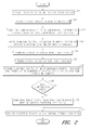
- FIG. 3 illustrates the steps performed by the storage subsystem 112 to configure the target system 100 in block 209 of FIG. 2 . These steps are preferably embodied in the FPGA download firmware 132 ( FIG. 1 ) executed by the controller 114 . In this example, it is assumed that the target system has multiple FPGAs 102 .
- step 301 the controller 114 places the storage subsystem 112 into an FPGA configuration mode. While in this mode, the storage subsystem 112 uses the data transfer protocol of the FPGA download interface specified by the download control information 122 to communicate with the FPGAs.
- step 302 the storage subsystem 112 asserts a busy signal to the interface controller 144 of the target system 100 to prevent the IDE-based communications from occurring between the storage subsystem 112 and the target system. This effectively frees some of the signal lines passed via the connectors 106 , 113 for use as FPGA download interface signal lines. Any appropriate mapping function may be used to map a subset of the connector signal lines to the download interface signal lines of the FPGAs, and different mappings may be used for different types and brands of FPGAs.
- the FPGA configuration files 120 are placed in the buffer 116 of the storage subsystem 112 so that they may be streamed/clocked to the FPGAs 102 .
- the configuration data represented in the FPGA configuration files 120 is then serially clocked out from the buffer 116 and into the FPGAs 102 in accordance with the protocol of the selected FPGA download interface.
- the storage subsystem 112 communicates directly with the FPGAs 102 during this process. If the FPGAs 102 are connected in a daisy chain configuration as illustrated, the configuration data is streamed serially to the first FPGA in the chain.
- the storage subsystem 112 may read back and verify this data; this may be accomplished via the firmware executed by the storage subsystem's controller 114 .
- step 306 the storage subsystem 112 de-asserts its busy signal to the interface controller 110 , and communications with the target system 100 as an ATA storage subsystem.
- Appropriate circuitry may be included in the target system 100 to isolate the FPGAs 102 from the interface controller 110 lines while the storage subsystem is in this mode.
- Examples download interfaces/protocols that may be implemented by storage subsystem 112 to configure Xilinx FPGAs are described in the Virtex-5 Series Configuration Architecture User Guide (UG191), available at http://www.xilinx.com/bvdocs/userguides/ug191.pdf, the disclosure of which is hereby incorporated by reference.
- Examples of download interfaces and protocols that may be implemented by storage subsystem 112 to configure Altera FPGAs are described in the Altera Configuration Handbook, Volumes 1 (CF5V1-2.4) and 2 (CF5V2-2.3), available from Altera Corporation and at www.altera.com/literature/hb/cfg/config_handbook.pdf, the disclosures of which are hereby incorporated by reference.
- the interface controller 110 may optionally be implemented in an FPGA 102 of the target system 100 , rather than separately. This may be accomplished by including the interface controller circuitry in the FPGA configuration files 120 streamed to the FPGAs. With this approach, once the configuration operation is complete, the first FPGA 102 in the daisy chain (if multiple FPGAs are included) would be capable of sending ATA storage commands (received from the processor 111 ) to the storage subsystem 112 in accordance with appropriate signal interface (USB, CF, PCMCIA, SATA, etc.).
- the storage subsystem 112 may implement one or more security features to protect the configuration data it stores.
- the configuration files 120 may optionally be stored on the storage subsystem 112 in an encrypted form to protect trade secrets.
- the subsystem configuration utility 160 FIG. 1
- the storage subsystem may encrypt these files 120 prior to or during transfer to the storage subsystem 112 , or the storage subsystem may encrypt these files as they are received.
- the configuration files 120 may be transferred to the target system 100 in encrypted form and then decrypted by the target system 100 .
- the storage subsystem 112 may initially partially configure one of the FPGAs 102 to implement a decryption circuit. This may be accomplished by sending appropriate (unencrypted) configuration data to this FPGA using partial configuration processes that are known in the art. Subsequently, as the storage subsystem 112 streams the encrypted configuration data 120 to the FPGAs, the decryption circuit would decrypt this data.
- the storage subsystem 112 may include an encryption key in its restricted space, and a microprocessor of the target system 100 may be programmed to retrieve this encryption key using a vendor-specific command. During the subsequent download process, this microprocessor could use the decryption key to decrypt the streamed configuration data.
- the storage subsystem 112 may also implement a vendor-specific purge command for rapidly and reliably purging the non-volatile memory array, as described in U.S. patent application Ser. No. 11/458,336, filed on Jul. 18, 2006, the disclosure of which is hereby incorporated herein by reference.
- the target system 100 may be designed to detect intrusion attempts, and to issue a purge command to the storage subsystem 112 when such an intrusion attempt or other tampering event is detected.
- the purge operation may, but need not, be a destructive operation that physically destroys or damages the non-volatile memory array 112 .
- the storage subsystem may also be configured to non-destructively purge the configuration file(s) 120 upon completion of the configuration process.
- the storage subsystem 112 may also be designed to password-protect the configuration files 120 , such that a user cannot read these files from the storage subsystem 112 without first entering a password on the host computer system.
- the password may be set by the configuration utility 160 ( FIG. 1 ) via a vendor-specific command when the configuration files 120 are copied to the storage subsystem 112 .
- the password would not have to be entered to cause the storage subsystem 112 to stream the configuration files 120 to the target system 100 .
- the storage subsystem 112 may, for example, be a solid-state memory card or drive that plugs into a slot or port of the target system 100 .
- the memory card or drive complies with at least one of the following card specifications: CompactFlash, PCMCIA, SmartMedia, MultiMediaCard, SecureDigital, Memory Stick, ATA/ATAPI, PCI Express, PCI Mezzanine Card, and AdvancedTCA Mezzanine Card.
- the storage subsystem 112 may, for example, have a housing and signal interface that complies with one of the following specifications: sub 1 inch hard disk drive, 1.8 inch hard disk drive, 2.5 inch hard disk drive and 3.5 inch hard disk drive. A custom form factor and/or signal interface may alternatively be used.
- the controller 114 comprises an ATA flash disk controller that executes firmware
- the firmware executed by the controller 114 embodies functionality for implementing the features described herein, including providing access to the restricted memory area of the NVM array 118 via vendor-specific commands.
- the controller 114 may alternatively be implemented in-whole or in-part as an ASIC, FPGA, or other device that does not execute firmware.
- the NVM array 118 may comprise, for example, flash integrated circuits, Chalcogenide RAM (C-RAM), Phase Change Memory (PC-RAM or PRAM), Programmable Metallization Cell RAM (PMC-RAM or PMCm), Ovonic Unified Memory (OUM), Resistance RAM (RRAM), NAND memory, NOR memory, EEPROM, Ferroelectric Memory (FeRAM), or other discrete NVM chips.
- C-RAM Chalcogenide RAM
- PC-RAM or PRAM Phase Change Memory
- PMC-RAM or PMCm Programmable Metallization Cell RAM
- OUM Ovonic Unified Memory
- RRAM Resistance RAM
- NAND memory NOR memory
- EEPROM Electrically erasable programmable Metallization Cell RAM
- FeRAM Ferroelectric Memory
Landscapes
- Engineering & Computer Science (AREA)
- Theoretical Computer Science (AREA)
- Human Computer Interaction (AREA)
- Physics & Mathematics (AREA)
- General Engineering & Computer Science (AREA)
- General Physics & Mathematics (AREA)
- Stored Programmes (AREA)
Abstract
Description
Claims (32)
Priority Applications (1)
| Application Number | Priority Date | Filing Date | Title |
|---|---|---|---|
| US11/554,453 US8161227B1 (en) | 2006-10-30 | 2006-10-30 | Storage subsystem capable of programming field-programmable devices of a target computer system |
Applications Claiming Priority (1)
| Application Number | Priority Date | Filing Date | Title |
|---|---|---|---|
| US11/554,453 US8161227B1 (en) | 2006-10-30 | 2006-10-30 | Storage subsystem capable of programming field-programmable devices of a target computer system |
Publications (1)
| Publication Number | Publication Date |
|---|---|
| US8161227B1 true US8161227B1 (en) | 2012-04-17 |
Family
ID=45931511
Family Applications (1)
| Application Number | Title | Priority Date | Filing Date |
|---|---|---|---|
| US11/554,453 Expired - Fee Related US8161227B1 (en) | 2006-10-30 | 2006-10-30 | Storage subsystem capable of programming field-programmable devices of a target computer system |
Country Status (1)
| Country | Link |
|---|---|
| US (1) | US8161227B1 (en) |
Cited By (130)
| Publication number | Priority date | Publication date | Assignee | Title |
|---|---|---|---|---|
| CN102999350A (en) * | 2012-10-24 | 2013-03-27 | 绵阳市维博电子有限责任公司 | FPGA (field-programmable gate array) program upgrading and online downloading method in digital signal processing platform |
| CN103729222A (en) * | 2013-12-30 | 2014-04-16 | 大唐移动通信设备有限公司 | Loading device and method of configuration file |
| US20140136766A1 (en) * | 2012-11-13 | 2014-05-15 | Ocz Technology Group, Inc. | Cache device for hard disk drives and methods of operation |
| US8898373B1 (en) | 2011-06-29 | 2014-11-25 | Western Digital Technologies, Inc. | System and method for improving wear-leveling performance in solid-state memory |
| US8917471B1 (en) | 2013-10-29 | 2014-12-23 | Western Digital Technologies, Inc. | Power management for data storage device |
| US8954653B1 (en) | 2012-06-26 | 2015-02-10 | Western Digital Technologies, Inc. | Mechanisms for efficient management of system data in data storage systems |
| US8954655B2 (en) | 2013-01-14 | 2015-02-10 | Western Digital Technologies, Inc. | Systems and methods of configuring a mode of operation in a solid-state memory |
| US8954694B2 (en) | 2012-11-15 | 2015-02-10 | Western Digital Technologies, Inc. | Methods, data storage devices and systems for fragmented firmware table rebuild in a solid state drive |
| US8959194B1 (en) | 2009-07-27 | 2015-02-17 | Juniper Networks, Inc. | Merging network device configuration schemas |
| US8959416B1 (en) | 2011-12-16 | 2015-02-17 | Western Digital Technologies, Inc. | Memory defect management using signature identification |
| US8959284B1 (en) | 2010-06-28 | 2015-02-17 | Western Digital Technologies, Inc. | Disk drive steering write data to write cache based on workload |
| US8966205B1 (en) | 2012-05-10 | 2015-02-24 | Western Digital Technologies, Inc. | System data management using garbage collection and hybrid self mapping |
| US8966343B2 (en) | 2012-08-21 | 2015-02-24 | Western Digital Technologies, Inc. | Solid-state drive retention monitor using reference blocks |
| US8966339B1 (en) | 2012-12-18 | 2015-02-24 | Western Digital Technologies, Inc. | Decoder supporting multiple code rates and code lengths for data storage systems |
| US8972655B2 (en) | 2013-01-21 | 2015-03-03 | Western Digital Technolgies, Inc. | Initialization of a storage device |
| US8972826B2 (en) | 2012-10-24 | 2015-03-03 | Western Digital Technologies, Inc. | Adaptive error correction codes for data storage systems |
| US8977804B1 (en) | 2011-11-21 | 2015-03-10 | Western Digital Technologies, Inc. | Varying data redundancy in storage systems |
| US8984247B1 (en) | 2012-05-10 | 2015-03-17 | Western Digital Technologies, Inc. | Storing and reconstructing mapping table data in a data storage system |
| US8990668B2 (en) | 2013-03-14 | 2015-03-24 | Western Digital Technologies, Inc. | Decoding data stored in solid-state memory |
| US9007841B1 (en) | 2013-10-24 | 2015-04-14 | Western Digital Technologies, Inc. | Programming scheme for improved voltage distribution in solid-state memory |
| US9007854B1 (en) | 2013-12-09 | 2015-04-14 | Western Digital Technologies, Inc. | Method and system for optimized soft decoding in a data storage device |
| US9013920B2 (en) | 2013-04-03 | 2015-04-21 | Western Digital Technologies, Inc. | Systems and methods of write precompensation to extend life of a solid-state memory |
| US9021168B1 (en) | 2011-09-06 | 2015-04-28 | Western Digital Technologies, Inc. | Systems and methods for an enhanced controller architecture in data storage systems |
| US9021339B2 (en) | 2012-11-29 | 2015-04-28 | Western Digital Technologies, Inc. | Data reliability schemes for data storage systems |
| US9021192B1 (en) | 2010-09-21 | 2015-04-28 | Western Digital Technologies, Inc. | System and method for enhancing processing of memory access requests |
| US9026716B2 (en) | 2010-05-12 | 2015-05-05 | Western Digital Technologies, Inc. | System and method for managing garbage collection in solid-state memory |
| US9032271B2 (en) | 2012-12-07 | 2015-05-12 | Western Digital Technologies, Inc. | System and method for lower page data recovery in a solid state drive |
| US9036283B1 (en) | 2014-01-22 | 2015-05-19 | Western Digital Technologies, Inc. | Data storage device with selective write to a first storage media or a second storage media |
| US9042197B2 (en) | 2013-07-23 | 2015-05-26 | Western Digital Technologies, Inc. | Power fail protection and recovery using low power states in a data storage device/system |
| US9053008B1 (en) | 2012-03-26 | 2015-06-09 | Western Digital Technologies, Inc. | Systems and methods for providing inline parameter service in data storage devices |
| US9058261B1 (en) | 2011-09-06 | 2015-06-16 | Western Digital Technologies, Inc. | Systems and methods for detailed error reporting in data storage systems |
| US9059742B1 (en) | 2013-03-15 | 2015-06-16 | Western Digital Technologies, Inc. | System and method for dynamic scaling of LDPC decoder in a solid state drive |
| US9058280B1 (en) | 2010-08-13 | 2015-06-16 | Western Digital Technologies, Inc. | Hybrid drive migrating data from disk to non-volatile semiconductor memory based on accumulated access time |
| US9059736B2 (en) | 2012-12-03 | 2015-06-16 | Western Digital Technologies, Inc. | Methods, solid state drive controllers and data storage devices having a runtime variable raid protection scheme |
| US9070379B2 (en) | 2013-08-28 | 2015-06-30 | Western Digital Technologies, Inc. | Data migration for data storage device |
| US9069475B1 (en) | 2010-10-26 | 2015-06-30 | Western Digital Technologies, Inc. | Hybrid drive selectively spinning up disk when powered on |
| US9081700B2 (en) | 2013-05-16 | 2015-07-14 | Western Digital Technologies, Inc. | High performance read-modify-write system providing line-rate merging of dataframe segments in hardware |
| US9110835B1 (en) | 2011-03-09 | 2015-08-18 | Western Digital Technologies, Inc. | System and method for improving a data redundancy scheme in a solid state subsystem with additional metadata |
| US9123686B2 (en) | 2013-04-12 | 2015-09-01 | Western Digital Technologies, Inc. | Thermal management for solid-state drive |
| US9122625B1 (en) | 2012-12-18 | 2015-09-01 | Western Digital Technologies, Inc. | Error correcting code encoder supporting multiple code rates and throughput speeds for data storage systems |
| US9141176B1 (en) | 2013-07-29 | 2015-09-22 | Western Digital Technologies, Inc. | Power management for data storage device |
| US9164886B1 (en) | 2010-09-21 | 2015-10-20 | Western Digital Technologies, Inc. | System and method for multistage processing in a memory storage subsystem |
| US9170932B1 (en) | 2012-05-22 | 2015-10-27 | Western Digital Technologies, Inc. | System data storage mechanism providing coherency and segmented data loading |
| US9170938B1 (en) | 2013-05-17 | 2015-10-27 | Western Digital Technologies, Inc. | Method and system for atomically writing scattered information in a solid state storage device |
| US9176859B2 (en) | 2009-01-07 | 2015-11-03 | Siliconsystems, Inc. | Systems and methods for improving the performance of non-volatile memory operations |
| US9177638B2 (en) | 2012-11-13 | 2015-11-03 | Western Digital Technologies, Inc. | Methods and devices for avoiding lower page corruption in data storage devices |
| US9182916B1 (en) | 2010-09-17 | 2015-11-10 | Western Digital Technologies, Inc. | Non-volatile storage subsystem with energy-based performance throttling |
| US9195530B1 (en) | 2011-09-06 | 2015-11-24 | Western Digital Technologies, Inc. | Systems and methods for improved data management in data storage systems |
| US9195293B1 (en) | 2013-05-03 | 2015-11-24 | Western Digital Technologies, Inc. | User controlled data storage device power and performance settings |
| US9208101B2 (en) | 2013-06-26 | 2015-12-08 | Western Digital Technologies, Inc. | Virtual NAND capacity extension in a hybrid drive |
| US9208020B2 (en) | 2012-06-26 | 2015-12-08 | Western Digital Technologies, Inc. | Efficient error handling mechanisms in data storage systems |
| US9214963B1 (en) | 2012-12-21 | 2015-12-15 | Western Digital Technologies, Inc. | Method and system for monitoring data channel to enable use of dynamically adjustable LDPC coding parameters in a data storage system |
| US9218279B2 (en) | 2013-03-15 | 2015-12-22 | Western Digital Technologies, Inc. | Atomic write command support in a solid state drive |
| US9253034B1 (en) | 2009-06-01 | 2016-02-02 | Juniper Networks, Inc. | Mass activation of network devices |
| US9250994B1 (en) | 2014-02-05 | 2016-02-02 | Western Digital Technologies, Inc. | Non-binary low-density parity check (LDPC) decoding using trellis maximization |
| US9263136B1 (en) | 2013-09-04 | 2016-02-16 | Western Digital Technologies, Inc. | Data retention flags in solid-state drives |
| US9270296B1 (en) | 2013-11-13 | 2016-02-23 | Western Digital Technologies, Inc. | Method and system for soft decoding through single read |
| US9268701B1 (en) | 2011-11-21 | 2016-02-23 | Western Digital Technologies, Inc. | Caching of data in data storage systems by managing the size of read and write cache based on a measurement of cache reliability |
| US9268487B2 (en) | 2014-03-24 | 2016-02-23 | Western Digital Technologies, Inc. | Method and apparatus for restricting writes to solid state memory when an end-of life condition is reached |
| US9274978B2 (en) | 2013-06-10 | 2016-03-01 | Western Digital Technologies, Inc. | Migration of encrypted data for data storage systems |
| US9275741B1 (en) | 2014-09-10 | 2016-03-01 | Western Digital Technologies, Inc. | Temperature compensation management in solid-state memory |
| US9274966B1 (en) | 2013-02-20 | 2016-03-01 | Western Digital Technologies, Inc. | Dynamically throttling host commands to disk drives |
| US9280200B1 (en) | 2013-05-20 | 2016-03-08 | Western Digital Technologies, Inc. | Automatic peak current throttle of tiered storage elements |
| US9280472B1 (en) | 2013-03-13 | 2016-03-08 | Western Digital Technologies, Inc. | Caching data in a high performance zone of a data storage system |
| US9286176B1 (en) | 2013-11-08 | 2016-03-15 | Western Digital Technologies, Inc. | Selective skipping of blocks in an SSD |
| US9304560B2 (en) | 2013-06-19 | 2016-04-05 | Western Digital Technologies, Inc. | Backup power for reducing host current transients |
| US9304709B2 (en) | 2013-09-06 | 2016-04-05 | Western Digital Technologies, Inc. | High performance system providing selective merging of dataframe segments in hardware |
| US9323467B2 (en) | 2013-10-29 | 2016-04-26 | Western Digital Technologies, Inc. | Data storage device startup |
| US9330143B2 (en) | 2013-10-24 | 2016-05-03 | Western Digital Technologies, Inc. | Data storage device supporting accelerated database operations |
| US9338927B2 (en) | 2013-05-02 | 2016-05-10 | Western Digital Technologies, Inc. | Thermal interface material pad and method of forming the same |
| US9335950B2 (en) | 2013-03-15 | 2016-05-10 | Western Digital Technologies, Inc. | Multiple stream compression and formatting of data for data storage systems |
| US9337864B1 (en) | 2014-01-29 | 2016-05-10 | Western Digital Technologies, Inc. | Non-binary LDPC decoder using binary subgroup processing |
| US9348741B1 (en) | 2011-12-19 | 2016-05-24 | Western Digital Technologies, Inc. | Systems and methods for handling write data access requests in data storage devices |
| US9348520B2 (en) | 2014-03-24 | 2016-05-24 | Western Digital Technologies, Inc. | Lifetime extension of non-volatile semiconductor memory for data storage device |
| US9354955B1 (en) | 2014-03-19 | 2016-05-31 | Western Digital Technologies, Inc. | Partial garbage collection for fast error handling and optimized garbage collection for the invisible band |
| US9361044B2 (en) | 2011-03-28 | 2016-06-07 | Western Digital Technologies, Inc. | Power-safe data management system |
| US9384088B1 (en) | 2014-02-24 | 2016-07-05 | Western Digital Technologies, Inc. | Double writing map table entries in a data storage system to guard against silent corruption |
| US9405617B1 (en) | 2011-02-11 | 2016-08-02 | Western Digital Technologies, Inc. | System and method for data error recovery in a solid state subsystem |
| US9405675B1 (en) | 2010-05-11 | 2016-08-02 | Western Digital Technologies, Inc. | System and method for managing execution of internal commands and host commands in a solid-state memory |
| US9405356B1 (en) | 2014-10-21 | 2016-08-02 | Western Digital Technologies, Inc. | Temperature compensation in data storage device |
| US9418699B1 (en) | 2014-10-09 | 2016-08-16 | Western Digital Technologies, Inc. | Management of sequentially written data |
| US9436630B2 (en) | 2013-06-11 | 2016-09-06 | Western Digital Technologies, Inc. | Using dual phys to support multiple PCIe link widths |
| US9442668B1 (en) | 2013-08-29 | 2016-09-13 | Western Digital Technologies, Inc. | Adaptive power management control with performance feedback |
| US9448738B2 (en) | 2013-03-15 | 2016-09-20 | Western Digital Technologies, Inc. | Compression and formatting of data for data storage systems |
| US9448742B2 (en) | 2014-03-27 | 2016-09-20 | Western Digital Technologies, Inc. | Communication between a host and a secondary storage device |
| US9454474B2 (en) | 2013-03-05 | 2016-09-27 | Western Digital Technologies, Inc. | Methods, devices and systems for two stage power-on map rebuild with free space accounting in a solid state drive |
| US9472222B2 (en) | 2014-05-16 | 2016-10-18 | Western Digital Technologies, Inc. | Vibration mitigation for a data storage device |
| US9489296B1 (en) | 2012-10-17 | 2016-11-08 | Western Digital Technologies, Inc. | Methods, devices and systems for hardware-based garbage collection in solid state drives |
| US9507523B1 (en) | 2012-10-12 | 2016-11-29 | Western Digital Technologies, Inc. | Methods, devices and systems for variable size logical page management in a solid state drive |
| US9529710B1 (en) | 2013-12-06 | 2016-12-27 | Western Digital Technologies, Inc. | Interleaved channels in a solid-state drive |
| US9542287B1 (en) | 2011-09-06 | 2017-01-10 | Western Digital Technologies, Inc. | Systems and methods for error injection in data storage systems |
| US9564212B2 (en) | 2014-05-06 | 2017-02-07 | Western Digital Technologies, Inc. | Solid-state memory corruption mitigation |
| US9583153B1 (en) | 2013-06-28 | 2017-02-28 | Western Digital Technologies, Inc. | Memory card placement within a solid state drive |
| US9620226B1 (en) | 2015-10-30 | 2017-04-11 | Western Digital Technologies, Inc. | Data retention charge loss and read disturb compensation in solid-state data storage systems |
| US9619317B1 (en) | 2012-12-18 | 2017-04-11 | Western Digital Technologies, Inc. | Decoder having early decoding termination detection |
| US9641378B1 (en) | 2013-03-12 | 2017-05-02 | Western Digital Technologies, Inc. | Adjustment of compression ratios for data storage |
| US9652379B1 (en) | 2010-09-15 | 2017-05-16 | Western Digital Technologies, Inc. | System and method for reducing contentions in solid-state memory access |
| US9668337B2 (en) | 2015-09-08 | 2017-05-30 | Western Digital Technologies, Inc. | Temperature management in data storage devices |
| US9665501B1 (en) | 2013-06-18 | 2017-05-30 | Western Digital Technologies, Inc. | Self-encrypting data storage device supporting object-level encryption |
| US9690696B1 (en) | 2014-05-14 | 2017-06-27 | Western Digital Technologies, Inc. | Lifetime extension of memory for data storage system |
| US9727261B2 (en) | 2015-09-24 | 2017-08-08 | Western Digital Technologies, Inc. | Weighted programming patterns in solid-state data storage systems |
| US9740248B2 (en) | 2013-06-07 | 2017-08-22 | Western Digital Technologies, Inc. | Component placement within a solid state drive |
| US9753847B2 (en) | 2009-10-27 | 2017-09-05 | Western Digital Technologies, Inc. | Non-volatile semiconductor memory segregating sequential, random, and system data to reduce garbage collection for page based mapping |
| EP3226418A1 (en) * | 2016-03-29 | 2017-10-04 | Illinois Tool Works, Inc. | Welding-type system with field programmable hardware |
| US9785563B1 (en) | 2015-08-13 | 2017-10-10 | Western Digital Technologies, Inc. | Read command processing for data storage system based on previous writes |
| US9823859B2 (en) | 2014-11-06 | 2017-11-21 | Western Digital Technologies, Inc. | Mechanical shock mitigation for data storage |
| US9830257B1 (en) | 2013-06-12 | 2017-11-28 | Western Digital Technologies, Inc. | Fast saving of data during power interruption in data storage systems |
| US9836232B1 (en) | 2015-09-30 | 2017-12-05 | Western Digital Technologies, Inc. | Data storage device and method for using secondary non-volatile memory for temporary metadata storage |
| US9857995B1 (en) | 2015-03-09 | 2018-01-02 | Western Digital Technologies, Inc. | Data storage device and method providing non-volatile memory buffer for real-time primary non-volatile memory protection |
| CN107944128A (en) * | 2017-11-21 | 2018-04-20 | 上海航天测控通信研究所 | The bad block simulation checking systems of FLASH based on storage control FPGA |
| US9977612B1 (en) | 2012-05-11 | 2018-05-22 | Western Digital Technologies, Inc. | System data management using garbage collection and logs |
| US10013174B2 (en) | 2015-09-30 | 2018-07-03 | Western Digital Technologies, Inc. | Mapping system selection for data storage device |
| US10079048B2 (en) | 2009-03-24 | 2018-09-18 | Western Digital Technologies, Inc. | Adjusting access of non-volatile semiconductor memory based on access time |
| US10126981B1 (en) | 2015-12-14 | 2018-11-13 | Western Digital Technologies, Inc. | Tiered storage using storage class memory |
| US10140067B1 (en) | 2013-12-19 | 2018-11-27 | Western Digital Technologies, Inc. | Data management for data storage device with multiple types of non-volatile memory media |
| CN109101262A (en) * | 2018-08-16 | 2018-12-28 | 郑州云海信息技术有限公司 | A kind of FPGA Configuration Online method and system |
| US20190155767A1 (en) * | 2017-11-17 | 2019-05-23 | Samsung Electronics Co., Ltd. | Storage device configured to update field programmable gate array and method of operating the same |
| US10387303B2 (en) | 2016-08-16 | 2019-08-20 | Western Digital Technologies, Inc. | Non-volatile storage system with compute engine to accelerate big data applications |
| US10417123B1 (en) | 2013-05-16 | 2019-09-17 | Western Digital Technologies, Inc. | Systems and methods for improving garbage collection and wear leveling performance in data storage systems |
| US10444998B1 (en) | 2013-10-24 | 2019-10-15 | Western Digital Technologies, Inc. | Data storage device providing data maintenance services |
| US10459644B2 (en) | 2016-10-28 | 2019-10-29 | Western Digital Techologies, Inc. | Non-volatile storage system with integrated compute engine and optimized use of local fast memory |
| US10545819B1 (en) | 2013-03-12 | 2020-01-28 | Western Digital Technologies, Inc. | Soft-decision input generation for data storage systems |
| US10565123B2 (en) | 2017-04-10 | 2020-02-18 | Western Digital Technologies, Inc. | Hybrid logical to physical address translation for non-volatile storage devices with integrated compute module |
| US20200134183A1 (en) * | 2018-10-25 | 2020-04-30 | Dell Products, L.P. | System and method to recover fpga firmware over a sideband interface |
| US10740231B2 (en) | 2018-11-20 | 2020-08-11 | Western Digital Technologies, Inc. | Data access in data storage device including storage class memory |
| US10769062B2 (en) | 2018-10-01 | 2020-09-08 | Western Digital Technologies, Inc. | Fine granularity translation layer for data storage devices |
| US10956071B2 (en) | 2018-10-01 | 2021-03-23 | Western Digital Technologies, Inc. | Container key value store for data storage devices |
| US11016905B1 (en) | 2019-11-13 | 2021-05-25 | Western Digital Technologies, Inc. | Storage class memory access |
| US20210182052A1 (en) * | 2018-11-30 | 2021-06-17 | Tencent Technology (Shenzhen) Company Limited | Method, device, and apparatus for updating application program, and storage medium |
| US11249921B2 (en) | 2020-05-06 | 2022-02-15 | Western Digital Technologies, Inc. | Page modification encoding and caching |
Citations (9)
| Publication number | Priority date | Publication date | Assignee | Title |
|---|---|---|---|---|
| US5847577A (en) | 1995-02-24 | 1998-12-08 | Xilinx, Inc. | DRAM memory cell for programmable logic devices |
| US20050062497A1 (en) | 2003-09-23 | 2005-03-24 | Stmicroelectronics S.R.L. | Field programmable gate array device |
| US6961819B2 (en) * | 2002-04-26 | 2005-11-01 | Mips Technologies, Inc. | Method and apparatus for redirection of operations between interfaces |
| US7003619B1 (en) * | 2001-04-09 | 2006-02-21 | Matrix Semiconductor, Inc. | Memory device and method for storing and reading a file system structure in a write-once memory array |
| US20060038586A1 (en) | 2003-06-10 | 2006-02-23 | Renxin Xia | Apparatus and methods for communicating with programmable logic devices |
| US20060100723A1 (en) | 2004-10-29 | 2006-05-11 | Dynacity Technology (Hk) Limited | Modular multi-axis motion control and driving system and method thereof |
| US20060139053A1 (en) | 2004-12-23 | 2006-06-29 | Actel Corporation | Non-volatile memory configuration scheme for volatile-memory-based programmable circuits in an FPGA |
| US20090147570A1 (en) * | 2006-05-15 | 2009-06-11 | Apple Inc. | Use of 8-bit or higher a/d for nand cell value |
| US20100146202A1 (en) * | 2004-12-21 | 2010-06-10 | Falanx Microsystems As | Microprocessor systems |
-
2006
- 2006-10-30 US US11/554,453 patent/US8161227B1/en not_active Expired - Fee Related
Patent Citations (9)
| Publication number | Priority date | Publication date | Assignee | Title |
|---|---|---|---|---|
| US5847577A (en) | 1995-02-24 | 1998-12-08 | Xilinx, Inc. | DRAM memory cell for programmable logic devices |
| US7003619B1 (en) * | 2001-04-09 | 2006-02-21 | Matrix Semiconductor, Inc. | Memory device and method for storing and reading a file system structure in a write-once memory array |
| US6961819B2 (en) * | 2002-04-26 | 2005-11-01 | Mips Technologies, Inc. | Method and apparatus for redirection of operations between interfaces |
| US20060038586A1 (en) | 2003-06-10 | 2006-02-23 | Renxin Xia | Apparatus and methods for communicating with programmable logic devices |
| US20050062497A1 (en) | 2003-09-23 | 2005-03-24 | Stmicroelectronics S.R.L. | Field programmable gate array device |
| US20060100723A1 (en) | 2004-10-29 | 2006-05-11 | Dynacity Technology (Hk) Limited | Modular multi-axis motion control and driving system and method thereof |
| US20100146202A1 (en) * | 2004-12-21 | 2010-06-10 | Falanx Microsystems As | Microprocessor systems |
| US20060139053A1 (en) | 2004-12-23 | 2006-06-29 | Actel Corporation | Non-volatile memory configuration scheme for volatile-memory-based programmable circuits in an FPGA |
| US20090147570A1 (en) * | 2006-05-15 | 2009-06-11 | Apple Inc. | Use of 8-bit or higher a/d for nand cell value |
Non-Patent Citations (3)
| Title |
|---|
| Advance Product Specification for XILINX System ACE CompactFlash Solution, DS080 (v1.5), Apr. 5, 2002. |
| Knipper, G., System ACE Configuration Solutions for Xilinx FPGAs, White Paper: System ACE, XILINX WP151 (v2.0), May 18, 2006. |
| XILINX System ACE Configuration Solutions FAQ Brochure. |
Cited By (173)
| Publication number | Priority date | Publication date | Assignee | Title |
|---|---|---|---|---|
| US9176859B2 (en) | 2009-01-07 | 2015-11-03 | Siliconsystems, Inc. | Systems and methods for improving the performance of non-volatile memory operations |
| US10079048B2 (en) | 2009-03-24 | 2018-09-18 | Western Digital Technologies, Inc. | Adjusting access of non-volatile semiconductor memory based on access time |
| US9253034B1 (en) | 2009-06-01 | 2016-02-02 | Juniper Networks, Inc. | Mass activation of network devices |
| US8959194B1 (en) | 2009-07-27 | 2015-02-17 | Juniper Networks, Inc. | Merging network device configuration schemas |
| US9753847B2 (en) | 2009-10-27 | 2017-09-05 | Western Digital Technologies, Inc. | Non-volatile semiconductor memory segregating sequential, random, and system data to reduce garbage collection for page based mapping |
| US9405675B1 (en) | 2010-05-11 | 2016-08-02 | Western Digital Technologies, Inc. | System and method for managing execution of internal commands and host commands in a solid-state memory |
| US9026716B2 (en) | 2010-05-12 | 2015-05-05 | Western Digital Technologies, Inc. | System and method for managing garbage collection in solid-state memory |
| US8959284B1 (en) | 2010-06-28 | 2015-02-17 | Western Digital Technologies, Inc. | Disk drive steering write data to write cache based on workload |
| US9058280B1 (en) | 2010-08-13 | 2015-06-16 | Western Digital Technologies, Inc. | Hybrid drive migrating data from disk to non-volatile semiconductor memory based on accumulated access time |
| US9652379B1 (en) | 2010-09-15 | 2017-05-16 | Western Digital Technologies, Inc. | System and method for reducing contentions in solid-state memory access |
| US9182916B1 (en) | 2010-09-17 | 2015-11-10 | Western Digital Technologies, Inc. | Non-volatile storage subsystem with energy-based performance throttling |
| US9021192B1 (en) | 2010-09-21 | 2015-04-28 | Western Digital Technologies, Inc. | System and method for enhancing processing of memory access requests |
| US9477413B2 (en) | 2010-09-21 | 2016-10-25 | Western Digital Technologies, Inc. | System and method for managing access requests to a memory storage subsystem |
| US9164886B1 (en) | 2010-09-21 | 2015-10-20 | Western Digital Technologies, Inc. | System and method for multistage processing in a memory storage subsystem |
| US10048875B2 (en) | 2010-09-21 | 2018-08-14 | Western Digital Technologies, Inc. | System and method for managing access requests to a memory storage subsystem |
| US9069475B1 (en) | 2010-10-26 | 2015-06-30 | Western Digital Technologies, Inc. | Hybrid drive selectively spinning up disk when powered on |
| US9405617B1 (en) | 2011-02-11 | 2016-08-02 | Western Digital Technologies, Inc. | System and method for data error recovery in a solid state subsystem |
| US9110835B1 (en) | 2011-03-09 | 2015-08-18 | Western Digital Technologies, Inc. | System and method for improving a data redundancy scheme in a solid state subsystem with additional metadata |
| US10496535B2 (en) | 2011-03-28 | 2019-12-03 | Western Digital Technologies, Inc. | Power-safe data management system |
| US9361044B2 (en) | 2011-03-28 | 2016-06-07 | Western Digital Technologies, Inc. | Power-safe data management system |
| US10025712B2 (en) | 2011-03-28 | 2018-07-17 | Western Digital Technologies, Inc. | Power-safe data management system |
| US8898373B1 (en) | 2011-06-29 | 2014-11-25 | Western Digital Technologies, Inc. | System and method for improving wear-leveling performance in solid-state memory |
| US9021168B1 (en) | 2011-09-06 | 2015-04-28 | Western Digital Technologies, Inc. | Systems and methods for an enhanced controller architecture in data storage systems |
| US9195530B1 (en) | 2011-09-06 | 2015-11-24 | Western Digital Technologies, Inc. | Systems and methods for improved data management in data storage systems |
| US9542287B1 (en) | 2011-09-06 | 2017-01-10 | Western Digital Technologies, Inc. | Systems and methods for error injection in data storage systems |
| US9058261B1 (en) | 2011-09-06 | 2015-06-16 | Western Digital Technologies, Inc. | Systems and methods for detailed error reporting in data storage systems |
| US8977804B1 (en) | 2011-11-21 | 2015-03-10 | Western Digital Technologies, Inc. | Varying data redundancy in storage systems |
| US9898406B2 (en) | 2011-11-21 | 2018-02-20 | Western Digital Technologies, Inc. | Caching of data in data storage systems by managing the size of read and write cache based on a measurement of cache reliability |
| US9268701B1 (en) | 2011-11-21 | 2016-02-23 | Western Digital Technologies, Inc. | Caching of data in data storage systems by managing the size of read and write cache based on a measurement of cache reliability |
| US9268657B1 (en) | 2011-11-21 | 2016-02-23 | Western Digital Technologies, Inc. | Varying data redundancy in storage systems |
| US8959416B1 (en) | 2011-12-16 | 2015-02-17 | Western Digital Technologies, Inc. | Memory defect management using signature identification |
| US9348741B1 (en) | 2011-12-19 | 2016-05-24 | Western Digital Technologies, Inc. | Systems and methods for handling write data access requests in data storage devices |
| US9053008B1 (en) | 2012-03-26 | 2015-06-09 | Western Digital Technologies, Inc. | Systems and methods for providing inline parameter service in data storage devices |
| US8984247B1 (en) | 2012-05-10 | 2015-03-17 | Western Digital Technologies, Inc. | Storing and reconstructing mapping table data in a data storage system |
| US8966205B1 (en) | 2012-05-10 | 2015-02-24 | Western Digital Technologies, Inc. | System data management using garbage collection and hybrid self mapping |
| US9977612B1 (en) | 2012-05-11 | 2018-05-22 | Western Digital Technologies, Inc. | System data management using garbage collection and logs |
| US11543974B2 (en) | 2012-05-22 | 2023-01-03 | Western Digital Technologies, Inc. | System data storage mechanism providing coherency and segmented data loading |
| US10379755B2 (en) | 2012-05-22 | 2019-08-13 | Western Digital Technologies, Inc. | System data storage mechanism providing coherency and segmented data loading |
| US10942656B2 (en) | 2012-05-22 | 2021-03-09 | Western Digital Technologies, Inc. | System data storage mechanism providing coherency and segmented data loading |
| US9170932B1 (en) | 2012-05-22 | 2015-10-27 | Western Digital Technologies, Inc. | System data storage mechanism providing coherency and segmented data loading |
| US9626118B2 (en) | 2012-06-26 | 2017-04-18 | Western Digital Technologies, Inc. | Efficient error handling mechanisms in data storage systems |
| US8954653B1 (en) | 2012-06-26 | 2015-02-10 | Western Digital Technologies, Inc. | Mechanisms for efficient management of system data in data storage systems |
| US9208020B2 (en) | 2012-06-26 | 2015-12-08 | Western Digital Technologies, Inc. | Efficient error handling mechanisms in data storage systems |
| US8966343B2 (en) | 2012-08-21 | 2015-02-24 | Western Digital Technologies, Inc. | Solid-state drive retention monitor using reference blocks |
| US9507523B1 (en) | 2012-10-12 | 2016-11-29 | Western Digital Technologies, Inc. | Methods, devices and systems for variable size logical page management in a solid state drive |
| US9489296B1 (en) | 2012-10-17 | 2016-11-08 | Western Digital Technologies, Inc. | Methods, devices and systems for hardware-based garbage collection in solid state drives |
| US10055345B2 (en) | 2012-10-17 | 2018-08-21 | Western Digital Technologies, Inc. | Methods, devices and systems for solid state drive control |
| US8972826B2 (en) | 2012-10-24 | 2015-03-03 | Western Digital Technologies, Inc. | Adaptive error correction codes for data storage systems |
| US10216574B2 (en) | 2012-10-24 | 2019-02-26 | Western Digital Technologies, Inc. | Adaptive error correction codes for data storage systems |
| CN102999350A (en) * | 2012-10-24 | 2013-03-27 | 绵阳市维博电子有限责任公司 | FPGA (field-programmable gate array) program upgrading and online downloading method in digital signal processing platform |
| US9417819B2 (en) * | 2012-11-13 | 2016-08-16 | Toshiba, Corporation | Cache device for hard disk drives and methods of operations |
| US9177638B2 (en) | 2012-11-13 | 2015-11-03 | Western Digital Technologies, Inc. | Methods and devices for avoiding lower page corruption in data storage devices |
| US20140136766A1 (en) * | 2012-11-13 | 2014-05-15 | Ocz Technology Group, Inc. | Cache device for hard disk drives and methods of operation |
| US8954694B2 (en) | 2012-11-15 | 2015-02-10 | Western Digital Technologies, Inc. | Methods, data storage devices and systems for fragmented firmware table rebuild in a solid state drive |
| US9021339B2 (en) | 2012-11-29 | 2015-04-28 | Western Digital Technologies, Inc. | Data reliability schemes for data storage systems |
| US9059736B2 (en) | 2012-12-03 | 2015-06-16 | Western Digital Technologies, Inc. | Methods, solid state drive controllers and data storage devices having a runtime variable raid protection scheme |
| US9952939B1 (en) | 2012-12-07 | 2018-04-24 | Western Digital Technologies, Inc. | System and method for lower page data recovery in a solid state drive |
| US9032271B2 (en) | 2012-12-07 | 2015-05-12 | Western Digital Technologies, Inc. | System and method for lower page data recovery in a solid state drive |
| US9122625B1 (en) | 2012-12-18 | 2015-09-01 | Western Digital Technologies, Inc. | Error correcting code encoder supporting multiple code rates and throughput speeds for data storage systems |
| US9619317B1 (en) | 2012-12-18 | 2017-04-11 | Western Digital Technologies, Inc. | Decoder having early decoding termination detection |
| US8966339B1 (en) | 2012-12-18 | 2015-02-24 | Western Digital Technologies, Inc. | Decoder supporting multiple code rates and code lengths for data storage systems |
| US9495243B2 (en) | 2012-12-18 | 2016-11-15 | Western Digital Technologies, Inc. | Error correcting code encoder supporting multiple code rates and throughput speeds for data storage systems |
| US9214963B1 (en) | 2012-12-21 | 2015-12-15 | Western Digital Technologies, Inc. | Method and system for monitoring data channel to enable use of dynamically adjustable LDPC coding parameters in a data storage system |
| US8954655B2 (en) | 2013-01-14 | 2015-02-10 | Western Digital Technologies, Inc. | Systems and methods of configuring a mode of operation in a solid-state memory |
| US8972655B2 (en) | 2013-01-21 | 2015-03-03 | Western Digital Technolgies, Inc. | Initialization of a storage device |
| US9274966B1 (en) | 2013-02-20 | 2016-03-01 | Western Digital Technologies, Inc. | Dynamically throttling host commands to disk drives |
| US9817577B2 (en) | 2013-03-05 | 2017-11-14 | Western Digital Technologies, Inc. | Methods, devices and systems for two stage power-on map rebuild with free space accounting in a solid state drive |
| US9454474B2 (en) | 2013-03-05 | 2016-09-27 | Western Digital Technologies, Inc. | Methods, devices and systems for two stage power-on map rebuild with free space accounting in a solid state drive |
| US10545819B1 (en) | 2013-03-12 | 2020-01-28 | Western Digital Technologies, Inc. | Soft-decision input generation for data storage systems |
| US9641378B1 (en) | 2013-03-12 | 2017-05-02 | Western Digital Technologies, Inc. | Adjustment of compression ratios for data storage |
| US11074125B2 (en) | 2013-03-12 | 2021-07-27 | Western Digital Technologies, Inc. | Data storage system and method for decoding data based on extrapolated flipped-bit data |
| US9280472B1 (en) | 2013-03-13 | 2016-03-08 | Western Digital Technologies, Inc. | Caching data in a high performance zone of a data storage system |
| US8990668B2 (en) | 2013-03-14 | 2015-03-24 | Western Digital Technologies, Inc. | Decoding data stored in solid-state memory |
| US10389381B2 (en) | 2013-03-15 | 2019-08-20 | Western Digital Technologies, Inc. | System and method for dynamic scaling of LDPC decoder in a solid state drive |
| US9448738B2 (en) | 2013-03-15 | 2016-09-20 | Western Digital Technologies, Inc. | Compression and formatting of data for data storage systems |
| US10254983B2 (en) | 2013-03-15 | 2019-04-09 | Western Digital Technologies, Inc. | Atomic write command support in a solid state drive |
| US10951233B2 (en) | 2013-03-15 | 2021-03-16 | Western Digital Technologies, Inc. | System and method for decoding iterations and dynamic scaling |
| US9218279B2 (en) | 2013-03-15 | 2015-12-22 | Western Digital Technologies, Inc. | Atomic write command support in a solid state drive |
| US10055171B2 (en) | 2013-03-15 | 2018-08-21 | Western Digital Technologies, Inc. | Compression and formatting of data for data storage systems |
| US9335950B2 (en) | 2013-03-15 | 2016-05-10 | Western Digital Technologies, Inc. | Multiple stream compression and formatting of data for data storage systems |
| US9350391B1 (en) | 2013-03-15 | 2016-05-24 | Western Digital Technologies, Inc. | System and method for dynamic scaling of LDPC decoder in a solid state drive |
| US9594520B2 (en) | 2013-03-15 | 2017-03-14 | Western Digital Technologies, Inc. | Atomic write command support in a solid state drive |
| US9059742B1 (en) | 2013-03-15 | 2015-06-16 | Western Digital Technologies, Inc. | System and method for dynamic scaling of LDPC decoder in a solid state drive |
| US9985652B2 (en) | 2013-03-15 | 2018-05-29 | Western Digital Technologies, Inc. | System and method for dynamic scaling of LDPC decoder in a solid state drive |
| US9013920B2 (en) | 2013-04-03 | 2015-04-21 | Western Digital Technologies, Inc. | Systems and methods of write precompensation to extend life of a solid-state memory |
| US9123686B2 (en) | 2013-04-12 | 2015-09-01 | Western Digital Technologies, Inc. | Thermal management for solid-state drive |
| US9880594B2 (en) | 2013-04-12 | 2018-01-30 | Western Digital Technologies, Inc. | Thermal management for solid-state drive |
| US9338927B2 (en) | 2013-05-02 | 2016-05-10 | Western Digital Technologies, Inc. | Thermal interface material pad and method of forming the same |
| US9195293B1 (en) | 2013-05-03 | 2015-11-24 | Western Digital Technologies, Inc. | User controlled data storage device power and performance settings |
| US10417123B1 (en) | 2013-05-16 | 2019-09-17 | Western Digital Technologies, Inc. | Systems and methods for improving garbage collection and wear leveling performance in data storage systems |
| US9948322B1 (en) | 2013-05-16 | 2018-04-17 | Western Digital Technologies, Inc. | High performance read-modify-write system providing line-rate merging of dataframe segments in hardware |
| US9081700B2 (en) | 2013-05-16 | 2015-07-14 | Western Digital Technologies, Inc. | High performance read-modify-write system providing line-rate merging of dataframe segments in hardware |
| US9170938B1 (en) | 2013-05-17 | 2015-10-27 | Western Digital Technologies, Inc. | Method and system for atomically writing scattered information in a solid state storage device |
| US9513831B2 (en) | 2013-05-17 | 2016-12-06 | Western Digital Technologies, Inc. | Method and system for atomically writing scattered information in a solid state storage device |
| US9280200B1 (en) | 2013-05-20 | 2016-03-08 | Western Digital Technologies, Inc. | Automatic peak current throttle of tiered storage elements |
| US10289168B2 (en) | 2013-06-07 | 2019-05-14 | Western Digital Technologies, Inc. | Component placement within a solid state drive |
| US9740248B2 (en) | 2013-06-07 | 2017-08-22 | Western Digital Technologies, Inc. | Component placement within a solid state drive |
| US9274978B2 (en) | 2013-06-10 | 2016-03-01 | Western Digital Technologies, Inc. | Migration of encrypted data for data storage systems |
| US9436630B2 (en) | 2013-06-11 | 2016-09-06 | Western Digital Technologies, Inc. | Using dual phys to support multiple PCIe link widths |
| US9830257B1 (en) | 2013-06-12 | 2017-11-28 | Western Digital Technologies, Inc. | Fast saving of data during power interruption in data storage systems |
| US9665501B1 (en) | 2013-06-18 | 2017-05-30 | Western Digital Technologies, Inc. | Self-encrypting data storage device supporting object-level encryption |
| US9304560B2 (en) | 2013-06-19 | 2016-04-05 | Western Digital Technologies, Inc. | Backup power for reducing host current transients |
| US9208101B2 (en) | 2013-06-26 | 2015-12-08 | Western Digital Technologies, Inc. | Virtual NAND capacity extension in a hybrid drive |
| US9583153B1 (en) | 2013-06-28 | 2017-02-28 | Western Digital Technologies, Inc. | Memory card placement within a solid state drive |
| US9042197B2 (en) | 2013-07-23 | 2015-05-26 | Western Digital Technologies, Inc. | Power fail protection and recovery using low power states in a data storage device/system |
| US9141176B1 (en) | 2013-07-29 | 2015-09-22 | Western Digital Technologies, Inc. | Power management for data storage device |
| US9070379B2 (en) | 2013-08-28 | 2015-06-30 | Western Digital Technologies, Inc. | Data migration for data storage device |
| US9442668B1 (en) | 2013-08-29 | 2016-09-13 | Western Digital Technologies, Inc. | Adaptive power management control with performance feedback |
| US10109352B2 (en) | 2013-09-04 | 2018-10-23 | Western Digital Technologies, Inc. | Data retention flags in solid-state drives |
| US9263136B1 (en) | 2013-09-04 | 2016-02-16 | Western Digital Technologies, Inc. | Data retention flags in solid-state drives |
| US9620220B2 (en) | 2013-09-04 | 2017-04-11 | Western Digital Technologies, Inc. | Data retention flags in solid-state drives |
| US9304709B2 (en) | 2013-09-06 | 2016-04-05 | Western Digital Technologies, Inc. | High performance system providing selective merging of dataframe segments in hardware |
| US9760304B2 (en) | 2013-09-06 | 2017-09-12 | Western Digital Technologies, Inc. | High performance system for selective merging of dataframe segments |
| US10444998B1 (en) | 2013-10-24 | 2019-10-15 | Western Digital Technologies, Inc. | Data storage device providing data maintenance services |
| US9007841B1 (en) | 2013-10-24 | 2015-04-14 | Western Digital Technologies, Inc. | Programming scheme for improved voltage distribution in solid-state memory |
| US9330143B2 (en) | 2013-10-24 | 2016-05-03 | Western Digital Technologies, Inc. | Data storage device supporting accelerated database operations |
| US9323467B2 (en) | 2013-10-29 | 2016-04-26 | Western Digital Technologies, Inc. | Data storage device startup |
| US8917471B1 (en) | 2013-10-29 | 2014-12-23 | Western Digital Technologies, Inc. | Power management for data storage device |
| US9286176B1 (en) | 2013-11-08 | 2016-03-15 | Western Digital Technologies, Inc. | Selective skipping of blocks in an SSD |
| US9270296B1 (en) | 2013-11-13 | 2016-02-23 | Western Digital Technologies, Inc. | Method and system for soft decoding through single read |
| US9529710B1 (en) | 2013-12-06 | 2016-12-27 | Western Digital Technologies, Inc. | Interleaved channels in a solid-state drive |
| US9007854B1 (en) | 2013-12-09 | 2015-04-14 | Western Digital Technologies, Inc. | Method and system for optimized soft decoding in a data storage device |
| US10140067B1 (en) | 2013-12-19 | 2018-11-27 | Western Digital Technologies, Inc. | Data management for data storage device with multiple types of non-volatile memory media |
| CN103729222B (en) * | 2013-12-30 | 2017-03-15 | 大唐移动通信设备有限公司 | A kind of charger of configuration file and method |
| CN103729222A (en) * | 2013-12-30 | 2014-04-16 | 大唐移动通信设备有限公司 | Loading device and method of configuration file |
| US9036283B1 (en) | 2014-01-22 | 2015-05-19 | Western Digital Technologies, Inc. | Data storage device with selective write to a first storage media or a second storage media |
| US9748974B2 (en) | 2014-01-29 | 2017-08-29 | Western Digital Technologies, Inc. | Non-binary LDPC decoder using binary subgroup processing |
| US9337864B1 (en) | 2014-01-29 | 2016-05-10 | Western Digital Technologies, Inc. | Non-binary LDPC decoder using binary subgroup processing |
| US9250994B1 (en) | 2014-02-05 | 2016-02-02 | Western Digital Technologies, Inc. | Non-binary low-density parity check (LDPC) decoding using trellis maximization |
| US9384088B1 (en) | 2014-02-24 | 2016-07-05 | Western Digital Technologies, Inc. | Double writing map table entries in a data storage system to guard against silent corruption |
| US9354955B1 (en) | 2014-03-19 | 2016-05-31 | Western Digital Technologies, Inc. | Partial garbage collection for fast error handling and optimized garbage collection for the invisible band |
| US10061696B2 (en) | 2014-03-19 | 2018-08-28 | Western Digital Technologies, Inc. | Partial garbage collection for fast error handling and optimized garbage collection for the invisible band |
| US9348520B2 (en) | 2014-03-24 | 2016-05-24 | Western Digital Technologies, Inc. | Lifetime extension of non-volatile semiconductor memory for data storage device |
| US9268487B2 (en) | 2014-03-24 | 2016-02-23 | Western Digital Technologies, Inc. | Method and apparatus for restricting writes to solid state memory when an end-of life condition is reached |
| US9448742B2 (en) | 2014-03-27 | 2016-09-20 | Western Digital Technologies, Inc. | Communication between a host and a secondary storage device |
| US9564212B2 (en) | 2014-05-06 | 2017-02-07 | Western Digital Technologies, Inc. | Solid-state memory corruption mitigation |
| US9690696B1 (en) | 2014-05-14 | 2017-06-27 | Western Digital Technologies, Inc. | Lifetime extension of memory for data storage system |
| US9472222B2 (en) | 2014-05-16 | 2016-10-18 | Western Digital Technologies, Inc. | Vibration mitigation for a data storage device |
| US9672934B2 (en) | 2014-09-10 | 2017-06-06 | Western Digital Technologies, Inc. | Temperature compensation management in solid-state memory |
| US9275741B1 (en) | 2014-09-10 | 2016-03-01 | Western Digital Technologies, Inc. | Temperature compensation management in solid-state memory |
| US9418699B1 (en) | 2014-10-09 | 2016-08-16 | Western Digital Technologies, Inc. | Management of sequentially written data |
| US9405356B1 (en) | 2014-10-21 | 2016-08-02 | Western Digital Technologies, Inc. | Temperature compensation in data storage device |
| US9823859B2 (en) | 2014-11-06 | 2017-11-21 | Western Digital Technologies, Inc. | Mechanical shock mitigation for data storage |
| US9857995B1 (en) | 2015-03-09 | 2018-01-02 | Western Digital Technologies, Inc. | Data storage device and method providing non-volatile memory buffer for real-time primary non-volatile memory protection |
| US9785563B1 (en) | 2015-08-13 | 2017-10-10 | Western Digital Technologies, Inc. | Read command processing for data storage system based on previous writes |
| US9668337B2 (en) | 2015-09-08 | 2017-05-30 | Western Digital Technologies, Inc. | Temperature management in data storage devices |
| US10481809B2 (en) | 2015-09-24 | 2019-11-19 | Western Digital Technologies, Inc. | Read disturb compensation using weighted programming patterns |
| US9727261B2 (en) | 2015-09-24 | 2017-08-08 | Western Digital Technologies, Inc. | Weighted programming patterns in solid-state data storage systems |
| US9836232B1 (en) | 2015-09-30 | 2017-12-05 | Western Digital Technologies, Inc. | Data storage device and method for using secondary non-volatile memory for temporary metadata storage |
| US10013174B2 (en) | 2015-09-30 | 2018-07-03 | Western Digital Technologies, Inc. | Mapping system selection for data storage device |
| US9620226B1 (en) | 2015-10-30 | 2017-04-11 | Western Digital Technologies, Inc. | Data retention charge loss and read disturb compensation in solid-state data storage systems |
| US10126981B1 (en) | 2015-12-14 | 2018-11-13 | Western Digital Technologies, Inc. | Tiered storage using storage class memory |
| US10761777B2 (en) | 2015-12-14 | 2020-09-01 | Western Digital Technologies, Inc. | Tiered storage using storage class memory |
| EP3226418A1 (en) * | 2016-03-29 | 2017-10-04 | Illinois Tool Works, Inc. | Welding-type system with field programmable hardware |
| CN107390566A (en) * | 2016-03-29 | 2017-11-24 | 伊利诺斯工具制品有限公司 | Solder type system with field-programmable hardware |
| US10387303B2 (en) | 2016-08-16 | 2019-08-20 | Western Digital Technologies, Inc. | Non-volatile storage system with compute engine to accelerate big data applications |
| US10459644B2 (en) | 2016-10-28 | 2019-10-29 | Western Digital Techologies, Inc. | Non-volatile storage system with integrated compute engine and optimized use of local fast memory |
| US10565123B2 (en) | 2017-04-10 | 2020-02-18 | Western Digital Technologies, Inc. | Hybrid logical to physical address translation for non-volatile storage devices with integrated compute module |
| US20190155767A1 (en) * | 2017-11-17 | 2019-05-23 | Samsung Electronics Co., Ltd. | Storage device configured to update field programmable gate array and method of operating the same |
| US10754800B2 (en) * | 2017-11-17 | 2020-08-25 | Samsung Electronics Co., Ltd. | Storage device configured to update field programmable gate array and method of operating the same |
| CN107944128A (en) * | 2017-11-21 | 2018-04-20 | 上海航天测控通信研究所 | The bad block simulation checking systems of FLASH based on storage control FPGA |
| CN107944128B (en) * | 2017-11-21 | 2021-03-19 | 上海航天测控通信研究所 | FLASH bad block simulation verification system based on storage control FPGA |
| CN109101262A (en) * | 2018-08-16 | 2018-12-28 | 郑州云海信息技术有限公司 | A kind of FPGA Configuration Online method and system |
| US10769062B2 (en) | 2018-10-01 | 2020-09-08 | Western Digital Technologies, Inc. | Fine granularity translation layer for data storage devices |
| US10956071B2 (en) | 2018-10-01 | 2021-03-23 | Western Digital Technologies, Inc. | Container key value store for data storage devices |
| US11100228B2 (en) * | 2018-10-25 | 2021-08-24 | Dell Products, L.P. | System and method to recover FPGA firmware over a sideband interface |
| US20200134183A1 (en) * | 2018-10-25 | 2020-04-30 | Dell Products, L.P. | System and method to recover fpga firmware over a sideband interface |
| US10740231B2 (en) | 2018-11-20 | 2020-08-11 | Western Digital Technologies, Inc. | Data access in data storage device including storage class memory |
| US11169918B2 (en) | 2018-11-20 | 2021-11-09 | Western Digital Technologies, Inc. | Data access in data storage device including storage class memory |
| US20210182052A1 (en) * | 2018-11-30 | 2021-06-17 | Tencent Technology (Shenzhen) Company Limited | Method, device, and apparatus for updating application program, and storage medium |
| US11726770B2 (en) * | 2018-11-30 | 2023-08-15 | Tencent Technology (Shenzhen) Company Limited | Method, device, and apparatus for updating application program, and storage medium |
| US11016905B1 (en) | 2019-11-13 | 2021-05-25 | Western Digital Technologies, Inc. | Storage class memory access |
| US11249921B2 (en) | 2020-05-06 | 2022-02-15 | Western Digital Technologies, Inc. | Page modification encoding and caching |
Similar Documents
| Publication | Publication Date | Title |
|---|---|---|
| US8161227B1 (en) | Storage subsystem capable of programming field-programmable devices of a target computer system | |
| US9251381B1 (en) | Solid-state storage subsystem security solution | |
| US8464073B2 (en) | Method and system for secure data storage | |
| US10503934B2 (en) | Secure subsystem | |
| TWI479359B (en) | Command executing method, memory controller and memory storage apparatus | |
| US8761402B2 (en) | System and methods for digital content distribution | |
| US20130159733A1 (en) | Memory device which protects secure data, method of operating the memory device, and method of generating authentication information | |
| US20110264925A1 (en) | Securing data on a self-encrypting storage device | |
| CN108985111A (en) | Data storage device and firmware encryption and decryption method | |
| US20130212368A1 (en) | Data protecting method, memory controller and memory storage device | |
| US20160259583A1 (en) | Storage device, storage device system and information terminal | |
| JP2011514568A (en) | Write once memory device and storage subsystem of a computer comprising a write many memory device and associated method | |
| US20070239996A1 (en) | Method and apparatus for binding computer memory to motherboard | |
| US20150242640A1 (en) | Encryption key selection | |
| US7761654B2 (en) | System and method of utilizing off-chip memory | |
| US9176896B2 (en) | Method of managing aligned and unaligned data bands in a self encrypting solid state drive | |
| CN102982290B (en) | Memory storage and terminal device | |
| TWI522839B (en) | Storage device with multiple interfaces and multiple levels of data protection and related method thereof | |
| US11644983B2 (en) | Storage device having encryption | |
| US11232210B2 (en) | Secure firmware booting | |
| JP2017037497A (en) | Erasing system of nonvolatile storage device, nonvolatile storage device, external erasing device, and method | |
| US20160259567A1 (en) | Processing data storage commands for enclosure services | |
| KR101620685B1 (en) | Method and apparatus for managing time-out data stored | |
| Budd | PROPOSED U. 2 STORAGE PIN OUT FOR TELEMETRY APPLICATIONS | |
| CN118295583A (en) | Method for configuration management of memory device, memory controller, memory device, electronic device, host device, and computer-readable medium |
Legal Events
| Date | Code | Title | Description |
|---|---|---|---|
| AS | Assignment |
Owner name: SILICONSYSTEMS, INC., CALIFORNIA Free format text: ASSIGNMENT OF ASSIGNORS INTEREST;ASSIGNORS:DIGGS, MARK S.;MERRY, DAVID E., JR.;REEL/FRAME:018481/0326 Effective date: 20061101 |
|
| STCF | Information on status: patent grant |
Free format text: PATENTED CASE |
|
| FPAY | Fee payment |
Year of fee payment: 4 |
|
| AS | Assignment |
Owner name: WESTERN DIGITAL TECHNOLOGIES, INC., CALIFORNIA Free format text: ASSIGNMENT OF ASSIGNORS INTEREST;ASSIGNOR:SILICONSYSTEMS, INC.;REEL/FRAME:036872/0017 Effective date: 20151015 |
|
| AS | Assignment |
Owner name: WESTERN DIGITAL TECHNOLOGIES, INC., CALIFORNIA Free format text: ASSIGNMENT OF ASSIGNORS INTEREST;ASSIGNOR:SILICONSYSTEMS, INC.;REEL/FRAME:037936/0204 Effective date: 20151015 |
|
| AS | Assignment |
Owner name: JPMORGAN CHASE BANK, N.A., AS COLLATERAL AGENT, ILLINOIS Free format text: SECURITY AGREEMENT;ASSIGNOR:WESTERN DIGITAL TECHNOLOGIES, INC.;REEL/FRAME:038744/0481 Effective date: 20160512 Owner name: JPMORGAN CHASE BANK, N.A., AS COLLATERAL AGENT, ILLINOIS Free format text: SECURITY AGREEMENT;ASSIGNOR:WESTERN DIGITAL TECHNOLOGIES, INC.;REEL/FRAME:038722/0229 Effective date: 20160512 Owner name: U.S. BANK NATIONAL ASSOCIATION, AS COLLATERAL AGENT, CALIFORNIA Free format text: SECURITY AGREEMENT;ASSIGNOR:WESTERN DIGITAL TECHNOLOGIES, INC.;REEL/FRAME:038744/0281 Effective date: 20160512 Owner name: JPMORGAN CHASE BANK, N.A., AS COLLATERAL AGENT, IL Free format text: SECURITY AGREEMENT;ASSIGNOR:WESTERN DIGITAL TECHNOLOGIES, INC.;REEL/FRAME:038722/0229 Effective date: 20160512 Owner name: JPMORGAN CHASE BANK, N.A., AS COLLATERAL AGENT, IL Free format text: SECURITY AGREEMENT;ASSIGNOR:WESTERN DIGITAL TECHNOLOGIES, INC.;REEL/FRAME:038744/0481 Effective date: 20160512 Owner name: U.S. BANK NATIONAL ASSOCIATION, AS COLLATERAL AGEN Free format text: SECURITY AGREEMENT;ASSIGNOR:WESTERN DIGITAL TECHNOLOGIES, INC.;REEL/FRAME:038744/0281 Effective date: 20160512 |
|
| AS | Assignment |
Owner name: WESTERN DIGITAL TECHNOLOGIES, INC., CALIFORNIA Free format text: RELEASE BY SECURED PARTY;ASSIGNOR:U.S. BANK NATIONAL ASSOCIATION, AS COLLATERAL AGENT;REEL/FRAME:045501/0714 Effective date: 20180227 |
|
| FEPP | Fee payment procedure |
Free format text: MAINTENANCE FEE REMINDER MAILED (ORIGINAL EVENT CODE: REM.); ENTITY STATUS OF PATENT OWNER: LARGE ENTITY |
|
| LAPS | Lapse for failure to pay maintenance fees |
Free format text: PATENT EXPIRED FOR FAILURE TO PAY MAINTENANCE FEES (ORIGINAL EVENT CODE: EXP.); ENTITY STATUS OF PATENT OWNER: LARGE ENTITY |
|
| STCH | Information on status: patent discontinuation |
Free format text: PATENT EXPIRED DUE TO NONPAYMENT OF MAINTENANCE FEES UNDER 37 CFR 1.362 |
|
| FP | Lapsed due to failure to pay maintenance fee |
Effective date: 20200417 |
|
| AS | Assignment |
Owner name: WESTERN DIGITAL TECHNOLOGIES, INC., CALIFORNIA Free format text: RELEASE OF SECURITY INTEREST AT REEL 038744 FRAME 0481;ASSIGNOR:JPMORGAN CHASE BANK, N.A.;REEL/FRAME:058982/0556 Effective date: 20220203 |