US7999608B1 - Integrated RF notch filters - Google Patents
Integrated RF notch filters Download PDFInfo
- Publication number
- US7999608B1 US7999608B1 US12/496,419 US49641909A US7999608B1 US 7999608 B1 US7999608 B1 US 7999608B1 US 49641909 A US49641909 A US 49641909A US 7999608 B1 US7999608 B1 US 7999608B1
- Authority
- US
- United States
- Prior art keywords
- circuit
- notch filter
- enhancement circuit
- coupled
- enhancement
- Prior art date
- Legal status (The legal status is an assumption and is not a legal conclusion. Google has not performed a legal analysis and makes no representation as to the accuracy of the status listed.)
- Active
Links
- 238000000034 method Methods 0.000 claims abstract description 9
- 238000001914 filtration Methods 0.000 claims description 6
- 230000001939 inductive effect Effects 0.000 claims description 6
- 238000012546 transfer Methods 0.000 claims description 2
- 239000003990 capacitor Substances 0.000 description 10
- 238000010897 surface acoustic wave method Methods 0.000 description 7
- 238000013459 approach Methods 0.000 description 6
- 238000004891 communication Methods 0.000 description 5
- 238000013461 design Methods 0.000 description 4
- 238000010586 diagram Methods 0.000 description 4
- 230000000694 effects Effects 0.000 description 4
- 238000003780 insertion Methods 0.000 description 4
- 230000037431 insertion Effects 0.000 description 4
- 238000012986 modification Methods 0.000 description 2
- 230000004048 modification Effects 0.000 description 2
- 230000035945 sensitivity Effects 0.000 description 2
- 101000608720 Helianthus annuus 10 kDa late embryogenesis abundant protein Proteins 0.000 description 1
- 239000000919 ceramic Substances 0.000 description 1
- 150000001875 compounds Chemical class 0.000 description 1
- 230000008878 coupling Effects 0.000 description 1
- 238000010168 coupling process Methods 0.000 description 1
- 238000005859 coupling reaction Methods 0.000 description 1
- 238000006880 cross-coupling reaction Methods 0.000 description 1
- 230000007423 decrease Effects 0.000 description 1
- 238000005516 engineering process Methods 0.000 description 1
- 230000010354 integration Effects 0.000 description 1
- 230000002452 interceptive effect Effects 0.000 description 1
- 238000013507 mapping Methods 0.000 description 1
Images


Classifications
-
- H—ELECTRICITY
- H03—ELECTRONIC CIRCUITRY
- H03F—AMPLIFIERS
- H03F1/00—Details of amplifiers with only discharge tubes, only semiconductor devices or only unspecified devices as amplifying elements
- H03F1/08—Modifications of amplifiers to reduce detrimental influences of internal impedances of amplifying elements
- H03F1/22—Modifications of amplifiers to reduce detrimental influences of internal impedances of amplifying elements by use of cascode coupling, i.e. earthed cathode or emitter stage followed by earthed grid or base stage respectively
- H03F1/223—Modifications of amplifiers to reduce detrimental influences of internal impedances of amplifying elements by use of cascode coupling, i.e. earthed cathode or emitter stage followed by earthed grid or base stage respectively with MOSFET's
-
- H—ELECTRICITY
- H03—ELECTRONIC CIRCUITRY
- H03F—AMPLIFIERS
- H03F3/00—Amplifiers with only discharge tubes or only semiconductor devices as amplifying elements
- H03F3/189—High-frequency amplifiers, e.g. radio frequency amplifiers
- H03F3/19—High-frequency amplifiers, e.g. radio frequency amplifiers with semiconductor devices only
- H03F3/195—High-frequency amplifiers, e.g. radio frequency amplifiers with semiconductor devices only in integrated circuits
-
- H—ELECTRICITY
- H03—ELECTRONIC CIRCUITRY
- H03F—AMPLIFIERS
- H03F3/00—Amplifiers with only discharge tubes or only semiconductor devices as amplifying elements
- H03F3/45—Differential amplifiers
- H03F3/45071—Differential amplifiers with semiconductor devices only
- H03F3/45076—Differential amplifiers with semiconductor devices only characterised by the way of implementation of the active amplifying circuit in the differential amplifier
- H03F3/45179—Differential amplifiers with semiconductor devices only characterised by the way of implementation of the active amplifying circuit in the differential amplifier using MOSFET transistors as the active amplifying circuit
- H03F3/45183—Long tailed pairs
- H03F3/45188—Non-folded cascode stages
-
- H—ELECTRICITY
- H03—ELECTRONIC CIRCUITRY
- H03H—IMPEDANCE NETWORKS, e.g. RESONANT CIRCUITS; RESONATORS
- H03H11/00—Networks using active elements
- H03H11/02—Multiple-port networks
- H03H11/04—Frequency selective two-port networks
- H03H11/12—Frequency selective two-port networks using amplifiers with feedback
- H03H11/1213—Frequency selective two-port networks using amplifiers with feedback using transistor amplifiers
-
- H—ELECTRICITY
- H03—ELECTRONIC CIRCUITRY
- H03H—IMPEDANCE NETWORKS, e.g. RESONANT CIRCUITS; RESONATORS
- H03H7/00—Multiple-port networks comprising only passive electrical elements as network components
- H03H7/01—Frequency selective two-port networks
- H03H7/03—Frequency selective two-port networks comprising means for compensation of loss
-
- H—ELECTRICITY
- H03—ELECTRONIC CIRCUITRY
- H03H—IMPEDANCE NETWORKS, e.g. RESONANT CIRCUITS; RESONATORS
- H03H7/00—Multiple-port networks comprising only passive electrical elements as network components
- H03H7/01—Frequency selective two-port networks
- H03H7/12—Bandpass or bandstop filters with adjustable bandwidth and fixed centre frequency
-
- H—ELECTRICITY
- H03—ELECTRONIC CIRCUITRY
- H03H—IMPEDANCE NETWORKS, e.g. RESONANT CIRCUITS; RESONATORS
- H03H7/00—Multiple-port networks comprising only passive electrical elements as network components
- H03H7/01—Frequency selective two-port networks
- H03H7/17—Structural details of sub-circuits of frequency selective networks
- H03H7/1741—Comprising typical LC combinations, irrespective of presence and location of additional resistors
- H03H7/1791—Combined LC in shunt or branch path
-
- H—ELECTRICITY
- H03—ELECTRONIC CIRCUITRY
- H03F—AMPLIFIERS
- H03F2200/00—Indexing scheme relating to amplifiers
- H03F2200/294—Indexing scheme relating to amplifiers the amplifier being a low noise amplifier [LNA]
-
- H—ELECTRICITY
- H03—ELECTRONIC CIRCUITRY
- H03F—AMPLIFIERS
- H03F2200/00—Indexing scheme relating to amplifiers
- H03F2200/391—Indexing scheme relating to amplifiers the output circuit of an amplifying stage comprising an LC-network
-
- H—ELECTRICITY
- H03—ELECTRONIC CIRCUITRY
- H03F—AMPLIFIERS
- H03F2203/00—Indexing scheme relating to amplifiers with only discharge tubes or only semiconductor devices as amplifying elements covered by H03F3/00
- H03F2203/45—Indexing scheme relating to differential amplifiers
- H03F2203/45386—Indexing scheme relating to differential amplifiers the AAC comprising one or more coils in the source circuit
-
- H—ELECTRICITY
- H03—ELECTRONIC CIRCUITRY
- H03H—IMPEDANCE NETWORKS, e.g. RESONANT CIRCUITS; RESONATORS
- H03H11/00—Networks using active elements
- H03H11/02—Multiple-port networks
- H03H11/24—Frequency-independent attenuators
- H03H11/245—Frequency-independent attenuators using field-effect transistor
-
- H—ELECTRICITY
- H03—ELECTRONIC CIRCUITRY
- H03H—IMPEDANCE NETWORKS, e.g. RESONANT CIRCUITS; RESONATORS
- H03H7/00—Multiple-port networks comprising only passive electrical elements as network components
- H03H7/01—Frequency selective two-port networks
- H03H2007/013—Notch or bandstop filters
-
- H—ELECTRICITY
- H03—ELECTRONIC CIRCUITRY
- H03H—IMPEDANCE NETWORKS, e.g. RESONANT CIRCUITS; RESONATORS
- H03H11/00—Networks using active elements
- H03H11/02—Multiple-port networks
- H03H11/04—Frequency selective two-port networks
- H03H2011/0488—Notch or bandstop filters
Definitions
- the present invention relates generally to high-Q integrated filters for operation at RF frequencies and their associated tuning. More specifically but not exclusively, the present invention relates to shunt-type notch filters having coupled negative conductance elements.
- Filters find widespread use in radio transceivers, as shown in FIG. 1 . Filters such as those shown in FIG. 1 are used to limit noise while attenuating potentially interfering signals as well as spurious signals. Most communication systems require RF filters with sharp frequency responses (i.e., notches) that make monolithic integration difficult. As a result, RF filters typically use bulky technologies, such as surface acoustic wave (SAW) or ceramic resonators. It would therefore be desirable to find methods and apparatus to provide more flexible and more readily integratable RF filters, as well as provide other advantages.
- SAW surface acoustic wave
- the present invention is directed generally to filter enhancements.
- a pair of LC filters and a Q-enhancement circuit are described, which can be integrated to overcome problems associated with conventional filters as well as provide other advantages.
- the LC filters provide a sharp frequency notch, while the Q-enhancement circuit creates a negative conductance/resistance to improve the quality factor (Q) of the illustrated LC resonator, as well as other LC or other tuned resonators.
- the filters and Q-enhancement circuit can be integrated in various embodiments, they are suitable for use in a variety of radio transceiver applications where conventional circuits may be too bulky or expensive.
- the present invention is directed to a filter system comprising a resonate shunt-type LC notch filter and a Q-enhancement circuit coupled to the resonate shunt-type LC notch filter, with the Q-enhancement circuit configured to generate a negative resistance so as to at least partially offset a resistance in the notch filter.
- the present invention is directed to a filter system for use with a multi-band transceiver, the filter system comprising a plurality of switchable LNA inputs disposed to receive input signals from two or more LNA stages such that one LNA stage of the plurality of LNA stages is active at a particular time, an inductive load element, a capacitive element coupled to the inductive load element, a resonate shunt-type LC notch filter coupled to the capacitive element and load element and a Q-enhancement circuit coupled to the resonate shunt-type LC notch filter, wherein the resonate shunt-type LC notch filter is further coupled to ones of the plurality of LNAs responsive to selection of one of the switchable LNA inputs.
- the present invention is directed to a method of filtering a received signal in a transceiver, comprising providing a received signal to a notch filter system in the transceiver and filtering the received signal in the notch filter system, wherein the notch filter system includes an LC shunt circuit and a Q-enhancement circuit coupled to the LC shunt circuit, and wherein the Q-enhancement circuit generates a negative resistance to at least partially offset a resistance in the LC shunt circuit so as to enhance the Q of the notch filter system.
- FIG. 1 is a diagram of a full duplex radio transceiver and the transmit leakage signal
- FIG. 2 a is a diagram of an LNA and shunt-type LC notch filter without compensation
- FIG. 2 b is a diagram of an embodiment of a shunt-type LC filter with Q-enhancement, in accordance with aspects of the present invention
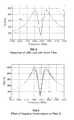
- FIG. 3 shows the frequency response of a shunt-type LC notch filter
- FIG. 4 illustrates the effect of negative conductance (provided by the Q-enhancement circuit) on the shunt-type LC notch filter, in accordance with aspects of the present invention
- FIG. 5 shows an embodiment of a differential LNA and shunt-type LC notch filter
- FIG. 6 shows an embodiment of a Q-enhancement circuit used to improve the performance of the shunt-type LC notch filter, in accordance with aspects of the present invention
- FIG. 7 shows an embodiment of an alternative Q-enhancement circuit used to improve the performance of the shunt-type LC notch filter, in accordance with aspects of the present invention
- FIG. 8 a is a plot of negative conductance sensitivity as a function of input signal level
- FIG. 8 b is a plot of negative conductance sensitivity as a function of temperature
- FIG. 9 is an embodiment of a circuit to realize a tunable resistor, in accordance with aspects of the present invention.
- FIG. 10 is an embodiment of an alternate circuit to realize a tunable resistor, in accordance with aspects of the present invention.
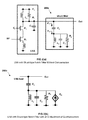
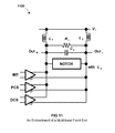
- FIG. 11 is a diagram of an embodiment of a multi-band front-end circuit with multiple LNAs feeding a single shunt-type LC notch filter, in accordance with aspects of the present invention.
- the RF downconverter In many communication systems an RF downcoverter, such as may be used in a transceiver, must be configured to accept a broad range of signals. In full duplex systems, the strongest of these is potentially the transmit leakage signal. This signal can easily overdrive the downconverting mixer and produce debilitating distortion. To prevent this, the RF downconverter generally includes a SAW filter after the LNA and before the mixer, as shown in circuit 100 of FIG. 1 .
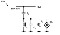
- FIG. 2 a shows an embodiment of a shunt-type notch filter 200 a that connects to the LNA output load.
- the notch filter presents an impedance transfer function with a zero at the transmit frequency f Tx and a pole at the receive frequency f Rx .
- the shunt-type notch filter consists of a parallel LC circuit and an impedance-transforming coupling capacitor C 3 .
- An imaginary resistor R 2 models the losses associated with the network. In practice, these losses degrade the filter's quality factor (Q) and the notch attenuation.
- Adding a negative conductance ⁇ G m to compensate the loss modeled by resistor R 2 can be used to enhance the filter system's Q value and correspondingly improve the notch's attenuation.
- the shunt network typically affects the load impedance of the LNA.
- the notch filter shorts out the load and attenuates the transmit leakage signal.
- the notch filter has little or no effect on the LNA load and the receive signal at the pole frequency ⁇ 4 .
- the shunt structure minimizes insertion loss and added noise.
- FIG. 3 shows the frequency response of the LNA load and notch filter system.
- the value of capacitor C 2 is adjusted first to position the zero and notch the transmit signal. Then, the value of capacitor C 1 is trimmed to resonate the combined load at the receive frequency. In practice, it is fairly straightforward to adjust these capacitors and tune the notch frequency over a wide bandwidth.
- the filter system's zero creates a notch in the response that attenuates the signal energy at the transmit frequency.
- the filter also adds a small capacitance to the LNA's output and shifts the load's resonance downward.
- the shunt structure of the filter advantageously introduces less than 1 dB insertion loss.
- the depth of the notch and the Q of the filter depend on the negative conductance (reciprocal resistance) ⁇ G m added to the parallel LC combination (and lossy element R 2 ) in the filter system.
- FIG. 4 illustrates this relationship. Note that even with the ⁇ G m value set 25% low, the attenuation approaches 15 dB.
- FIG. 5 illustrates an embodiment 500 of a differential structure using only two inductors and a negative conductance element ( ⁇ G m ) to enhance Q (Inductor L 1 is a center-tapped differential structure).
- the Q-enhancement circuit that connects across the parallel LC network senses the applied voltage and develops a current opposite to this voltage.
- the negative conductance ⁇ G m equals
- G m rms ⁇ ⁇ i out ⁇ ( t ) ⁇ rms ⁇ ⁇ v in ⁇ ( t ) ⁇ ( 7 )
- rms ⁇ ⁇ represents the root-mean-squared or effective value of the argument.
- the root-mean-squared value equals
- the amplified transmit leakage signal drives the Q-enhancement circuit towards large-signal operation.
- Capacitors C 4 couple the signal to the input transistors and allow independent biasing of the devices. These capacitors also form a capacitor divider with the gate-source capacitance of the MOS transistors that attenuates the input signal according to
- ⁇ v in v diff ⁇ C 4 C 4 + C gs ( 9 ) assuming an ac ground at the source-coupled node V s .
- the square-law behavior of the MOS devices makes the ⁇ G m value potentially sensitive to the amplitude of the input signal v in and consequently the transmit signal leakage level.
- the ⁇ G m value of the simple differential pair increases as the input signal level decreases.
- the ⁇ G m value falls at high temperatures due to the lower intrinsic gain of MOS transistors. This makes the ⁇ G m value sensitive to both the transmit power level and temperature.
- Adding a resistor R 3 to the differential pair as shown in circuit 700 of FIG. 7 reduces the variation in the circuit's transconductance. It accomplishes this by introducing local feedback that linearizes the MOSFET square-law response.
- the ⁇ G m value stays relatively constant as the amplitude of the input signal v in changes or the operating temperature changes as shown in FIG. 8 . Tuning becomes a little more challenging as the value of resistor R 3 must now be adjusted.
- FIG. 9 shows an embodiment 900 of the switched-resistor approach.
- the maximum value possible equals the value of resistor R 30 and occurs with all the switches S 1 ⁇ S n open. When switch S 1 closes, the effective resistance drops to
- R 3 R 30 ⁇ R 31 R 30 + R 31 ( 12 ) where R 31 >>R 30 to realize a small step.
- the large value of shunt resistor R 31 conveniently reduces the effect of the switch resistance.
- the low signal current flowing through this branch should also minimize any distortion due to the switch. Adding other switched-resistors extends the tuning range.
- FIG. 10 illustrates an embodiment 1000 of a variable MOSFET resistor. It uses a replica device (transistor N 10 ) and feedback circuit to adjust the resistance of the MOSFET device N 9 .
- r ds ⁇ ⁇ 10 I b ⁇ ⁇ 1 I b ⁇ ⁇ 2 ⁇ R 10 ( 14 ) which allows the variable resistor N 10 to be controlled by adjusting currents I b1 and I b2 .
- the operational amplifier also drives transistor N 9 and ensures its resistance tracks that of transistor N 10 .
- the resistance seen by the Q-enhancement differential pair then equals the parallel combination of the variable MOSFET resistance due to transistor N 9 and resistor R 30 .
- Q-enhancement circuits are possible and envisioned within the scope of the present invention. These two examples represent only a few possible structures that are provided for purposes of illustration, not limitation.
- other tuned or resonator circuits in addition to those LC circuits illustrated herein, may alternately be combined with a Q-enhancement circuit in various embodiments of the present invention so as to increase the Q value and enhance the filter notch characteristics.
- a filter system including the LC resonator and Q-enhancement circuit may further include switching elements configured to receive a transmit power level signal or other switching signal and selectively switch, in response to the transmit power level, the Q-enhancement circuit into or out of the filter system.
- the zero frequency ⁇ z may be shifted away and the Q-enhancement circuit may be disabled.
- the low insertion loss of the shunt filter ensures the LNA gain changes only slightly. This approach may be used to simplify the AGC system, save current, and/or extend battery life.
- SAW filters complicate the radio receiver.
- SAW devices are off-chip devices and as such add design complexity, require matching networks, occupy valuable PCB area, and operate only in specific bands. As such, they multiply as the number of radio bands increase.
- multi-band receivers rely on multiple low-noise amplifiers to interface to the front-end and antenna.
- Each LNA includes an inductive load and this consumes die area.
- integrating a notch filter for each band compounds this problem.
- An alternative approach in accordance with aspects of the present invention provides multi-band coverage using only two inductors as shown in embodiment 1100 of FIG. 11 .
- the unused LNA stages are switched off using the input bias voltage source (V b in FIG. 5 ) and the cascode devices. This adds some capacitance to the network which can be resonated out by the load inductor.
- Coarse-tuning capacitor structures allow a wide tuning range for the LNA load and notch filter.
- the Q-enhancement circuit compensates any filter losses.
- the shunt-type filter structure illustrated in the embodiments described previously may be used to provide a very high-Q notch response with minimal insertion loss. It uses an active ⁇ G m circuit to compensate for LC losses that otherwise degrade filter Q and lessen notch attenuation.
- the filter may be tuned easily by sliding capacitors C 1 and C 2 .
- the shunt structure minimizes effects on interstage matching.
- the notch filter easily extends to multi-band applications.
- the shunt-type notch filter provides an alternate approach to attenuate the transmit leakage signal and thus eliminate the need for a SAW filter in many communications applications.
- the present invention may be implemented as a notch filter subsystem of a communications device such as a transceiver.
- the functionality described herein may be integrated, in whole or in part, into an integrated monolithic device such as a communications chip (integrated circuit) along with other transceiver components and/or subsystems.
Landscapes
- Engineering & Computer Science (AREA)
- Power Engineering (AREA)
- Microelectronics & Electronic Packaging (AREA)
- Transceivers (AREA)
Abstract
Description
Y 2=1sL 2 +sC 2+1/R 2 (1)
Z f=1/(Y 2 −G m)+1/sC 3 (2)
which simplifies to
where G=1/R2−Gm and β=(C2+C3)/C2C3.
ωz=√{square root over (1/L 2(C 2 +C 3))}ωp=√{square root over (1/L 2 C 2)} (5)
Note that ωz<ω4 and this matches the relative positive of fTx and fRx. In practice, capacitor C3 should be kept small to position ωz close to ωp.
−1/G m =R 2 (6)
where rms { } represents the root-mean-squared or effective value of the argument. By definition, the root-mean-squared value equals
assuming an ac ground at the source-coupled node Vs. As such, the drain current for each device comprising the differential pair adheres to the square-law relationship where
i D5 =K 1(αv in +V bias−s −V s −V T)
i D6 =K 2(−αv in +V bias −V s −V T)2 (10)
with the intrinsic gain K representing ½ μCox(W/L). It follows then that the output current becomes simply
Δi out =i D6 −i D5 (11)
where the cross-coupling of the output realizes the negative conductance. It's important to note that the transconductance of the differential pair varies with the bias current Ibias and allows a straightforward means to adjust the −Gm value (and the notch attenuation).
where R31>>R30 to realize a small step. The large value of shunt resistor R31 conveniently reduces the effect of the switch resistance. Moreover, the low signal current flowing through this branch should also minimize any distortion due to the switch. Adding other switched-resistors extends the tuning range.
I b1 R 10 =V DS10 =I b2 r ds10 (13)
where rds10 represents the channel resistance of transistor N10. It follows that
which allows the variable resistor N10 to be controlled by adjusting currents Ib1 and Ib2. The operational amplifier also drives transistor N9 and ensures its resistance tracks that of transistor N10. The reference voltage Vref matches the nominal voltage seen at the source terminals of the differential pair N9-N10 with
V ref =V s =V bias −V T−√{square root over (I bias2K)} (15)
The resistance seen by the Q-enhancement differential pair then equals the parallel combination of the variable MOSFET resistance due to transistor N9 and resistor R30.
Claims (14)
Priority Applications (1)
| Application Number | Priority Date | Filing Date | Title |
|---|---|---|---|
| US12/496,419 US7999608B1 (en) | 2008-07-01 | 2009-07-01 | Integrated RF notch filters |
Applications Claiming Priority (2)
| Application Number | Priority Date | Filing Date | Title |
|---|---|---|---|
| US7743708P | 2008-07-01 | 2008-07-01 | |
| US12/496,419 US7999608B1 (en) | 2008-07-01 | 2009-07-01 | Integrated RF notch filters |
Publications (1)
| Publication Number | Publication Date |
|---|---|
| US7999608B1 true US7999608B1 (en) | 2011-08-16 |
Family
ID=44358553
Family Applications (1)
| Application Number | Title | Priority Date | Filing Date |
|---|---|---|---|
| US12/496,419 Active US7999608B1 (en) | 2008-07-01 | 2009-07-01 | Integrated RF notch filters |
Country Status (1)
| Country | Link |
|---|---|
| US (1) | US7999608B1 (en) |
Cited By (9)
| Publication number | Priority date | Publication date | Assignee | Title |
|---|---|---|---|---|
| US20110299634A1 (en) * | 2010-06-03 | 2011-12-08 | Broadcom Corporation | Saw-less receiver with a frequency translated bpf having a negative resistance |
| US20120322395A1 (en) * | 2010-02-24 | 2012-12-20 | M4S Ny | Rejection of rf interferers and noise in a wireless communications transceiver |
| WO2013119703A1 (en) * | 2012-02-07 | 2013-08-15 | Qualcomm Incorporated | Notch filter integrated in lna of a coexisting radio |
| US9306603B2 (en) | 2014-01-24 | 2016-04-05 | Qualcomm Incorporated | Tunable radio frequency (RF) front-end architecture using filter having adjustable inductance and capacitance |
| US20170012597A1 (en) * | 2015-07-07 | 2017-01-12 | Nokia Technologies Oy | Rf filter suppression tuning based on transmit power |
| US10979086B2 (en) * | 2017-11-07 | 2021-04-13 | Nordic Semiconductor Asa | Multi-band radio receivers |
| WO2022048932A1 (en) * | 2020-09-03 | 2022-03-10 | Novelda As | Filter |
| US11387857B2 (en) * | 2019-12-06 | 2022-07-12 | Silicon Laboratories Inc. | Dynamically reconfigurable frequency selective attenuator for radio frequency receiver front end |
| US11463064B2 (en) | 2019-12-06 | 2022-10-04 | Silicon Laboratories Inc. | Frequency selective attenuator for optimized radio frequency coexistence |
Citations (4)
| Publication number | Priority date | Publication date | Assignee | Title |
|---|---|---|---|---|
| US20080079497A1 (en) * | 2006-08-31 | 2008-04-03 | Texas Instruments | Low Noise Amplifier With Embedded Filter and Related Wireless Communication Unit |
| US7389098B2 (en) * | 2003-09-23 | 2008-06-17 | Information And Communication University Research And Industrial Cooperation Group | Heterodyne receiver for low noise and image frequency repression |
| US7522024B2 (en) * | 2007-04-06 | 2009-04-21 | Mediatek Inc. | Negative gm circuit, a filter and low noise amplifier including such a filter |
| US7885629B2 (en) * | 2006-08-03 | 2011-02-08 | Broadcom Corporation | Circuit with Q-enhancement cell having programmable bias current slope |
-
2009
- 2009-07-01 US US12/496,419 patent/US7999608B1/en active Active
Patent Citations (4)
| Publication number | Priority date | Publication date | Assignee | Title |
|---|---|---|---|---|
| US7389098B2 (en) * | 2003-09-23 | 2008-06-17 | Information And Communication University Research And Industrial Cooperation Group | Heterodyne receiver for low noise and image frequency repression |
| US7885629B2 (en) * | 2006-08-03 | 2011-02-08 | Broadcom Corporation | Circuit with Q-enhancement cell having programmable bias current slope |
| US20080079497A1 (en) * | 2006-08-31 | 2008-04-03 | Texas Instruments | Low Noise Amplifier With Embedded Filter and Related Wireless Communication Unit |
| US7522024B2 (en) * | 2007-04-06 | 2009-04-21 | Mediatek Inc. | Negative gm circuit, a filter and low noise amplifier including such a filter |
Cited By (14)
| Publication number | Priority date | Publication date | Assignee | Title |
|---|---|---|---|---|
| US20120322395A1 (en) * | 2010-02-24 | 2012-12-20 | M4S Ny | Rejection of rf interferers and noise in a wireless communications transceiver |
| US9166636B2 (en) * | 2010-02-24 | 2015-10-20 | Huawei Technologies Co., Ltd. | Rejection of RF interferers and noise in a wireless communications transceiver |
| US20160020793A1 (en) * | 2010-02-24 | 2016-01-21 | Huawei Technologies Co., Ltd. | Rejection of rf interferers and noise in a wireless communications transceiver |
| US20110299634A1 (en) * | 2010-06-03 | 2011-12-08 | Broadcom Corporation | Saw-less receiver with a frequency translated bpf having a negative resistance |
| WO2013119703A1 (en) * | 2012-02-07 | 2013-08-15 | Qualcomm Incorporated | Notch filter integrated in lna of a coexisting radio |
| US9306603B2 (en) | 2014-01-24 | 2016-04-05 | Qualcomm Incorporated | Tunable radio frequency (RF) front-end architecture using filter having adjustable inductance and capacitance |
| US20170012597A1 (en) * | 2015-07-07 | 2017-01-12 | Nokia Technologies Oy | Rf filter suppression tuning based on transmit power |
| US9960748B2 (en) * | 2015-07-07 | 2018-05-01 | Provenance Asset Group Llc | RF filter suppression tuning based on transmit power |
| US10979086B2 (en) * | 2017-11-07 | 2021-04-13 | Nordic Semiconductor Asa | Multi-band radio receivers |
| US11387857B2 (en) * | 2019-12-06 | 2022-07-12 | Silicon Laboratories Inc. | Dynamically reconfigurable frequency selective attenuator for radio frequency receiver front end |
| US11463064B2 (en) | 2019-12-06 | 2022-10-04 | Silicon Laboratories Inc. | Frequency selective attenuator for optimized radio frequency coexistence |
| US11973481B2 (en) | 2019-12-06 | 2024-04-30 | Silicon Laboratories Inc. | Frequency selective attenuator for optimized radio frequency coexistence |
| US11984866B2 (en) | 2019-12-06 | 2024-05-14 | Silicon Laboratories Inc. | Frequency selective attenuator for optimized radio frequency coexistence |
| WO2022048932A1 (en) * | 2020-09-03 | 2022-03-10 | Novelda As | Filter |
Similar Documents
| Publication | Publication Date | Title |
|---|---|---|
| US7999608B1 (en) | Integrated RF notch filters | |
| US7081796B2 (en) | Radio frequency low noise amplifier with automatic gain control | |
| US7266360B2 (en) | Low noise amplifier for wireless communications | |
| US6424222B1 (en) | Variable gain low noise amplifier for a wireless terminal | |
| US8081033B2 (en) | Variable gain amplifier and high-frequency signal receiving apparatus comprising the same | |
| US7522024B2 (en) | Negative gm circuit, a filter and low noise amplifier including such a filter | |
| US7714657B2 (en) | Low noise amplifier gain controlled scheme | |
| EP0886384A2 (en) | Single-stage dual-band low-noise amplifier for use in a wireless communication system receiver | |
| EP2947769B1 (en) | Low-noise amplifier | |
| US8005448B1 (en) | Radio frequency duplex filter for removing transmit signals from a receive path | |
| US7440729B2 (en) | Apparatus, methods and articles of manufacture for output impedance matching using multi-band signal processing | |
| US6630861B2 (en) | Variable gain amplifier | |
| CN116131770B (en) | High-integration-level high-linearity low-noise amplifier | |
| KR100789918B1 (en) | Input Matching Circuit of Wideband Low Noise Amplifier | |
| US6963247B2 (en) | Gain stabilization technique for narrow band integrated low noise amplifiers | |
| EP1447906B1 (en) | Dual gate low noise amplifier | |
| US5057791A (en) | Device and method for bi-directional amplification with a JFET | |
| KR100963816B1 (en) | Narrowband Multiband Low Noise Amplifier with Common Source Structure | |
| JP2581733B2 (en) | Monolithic integrated circuit, tuner circuit device, and receiver | |
| US7522017B1 (en) | High-Q integrated RF filters | |
| Lee et al. | CMOS tunable channel-selection LNA employing active feedback technique and gain-boosted N-path bandpass filter for advanced cellular applications | |
| KR100884159B1 (en) | Multi-frequency band impedance matching circuit using automatic matching capacitor | |
| US6992530B2 (en) | RF amplifier with improved impedance matching | |
| Dinh et al. | A dual-function filter for 5.25 ghz narrowband and 3.6 ghz-10.1 ghz ultrawideband systems | |
| Dali et al. | Entwicklung eines programmierbaren, rauscharmen Verstärkers für" Multistandard"-Empfänger in 65-nm-CMOS-Technologie |
Legal Events
| Date | Code | Title | Description |
|---|---|---|---|
| AS | Assignment |
Owner name: QUINTIC HOLDINGS, CALIFORNIA Free format text: ASSIGNMENT OF ASSIGNORS INTEREST;ASSIGNOR:SEQUOIA COMMUNICATIONS CORPORATION;REEL/FRAME:023639/0014 Effective date: 20091204 |
|
| STCF | Information on status: patent grant |
Free format text: PATENTED CASE |
|
| AS | Assignment |
Owner name: QUINTIC MICROELECTRONICS (WUXI) CO., LTD., CHINA Free format text: ASSIGNMENT OF ASSIGNORS INTEREST;ASSIGNOR:QUINTIC HOLDINGS;REEL/FRAME:034037/0541 Effective date: 20141015 |
|
| FEPP | Fee payment procedure |
Free format text: PAT HOLDER NO LONGER CLAIMS SMALL ENTITY STATUS, ENTITY STATUS SET TO UNDISCOUNTED (ORIGINAL EVENT CODE: STOL); ENTITY STATUS OF PATENT OWNER: LARGE ENTITY |
|
| AS | Assignment |
Owner name: QUINTIC MICROELECTRONICS (WUXI) CO., LTD., CHINA Free format text: ASSIGNMENT OF ASSIGNORS INTEREST;ASSIGNOR:NXP B.V.;REEL/FRAME:034747/0893 Effective date: 20150105 |
|
| AS | Assignment |
Owner name: QUINTIC MICROELECTRONICS (WUXI) CO., LTD., CHINA Free format text: ASSIGNMENT OF ASSIGNORS INTEREST;ASSIGNOR:NXP B.V.;REEL/FRAME:034752/0761 Effective date: 20150105 |
|
| AS | Assignment |
Owner name: NXP B.V., NETHERLANDS Free format text: ASSIGNMENT OF ASSIGNORS INTEREST;ASSIGNOR:QUINTIC MICROELECTRONICS (WUXI) CO., LTD.;REEL/FRAME:034854/0262 Effective date: 20150128 |
|
| REMI | Maintenance fee reminder mailed | ||
| FPAY | Fee payment |
Year of fee payment: 4 |
|
| SULP | Surcharge for late payment | ||
| MAFP | Maintenance fee payment |
Free format text: PAYMENT OF MAINTENANCE FEE, 8TH YEAR, LARGE ENTITY (ORIGINAL EVENT CODE: M1552); ENTITY STATUS OF PATENT OWNER: LARGE ENTITY Year of fee payment: 8 |
|
| MAFP | Maintenance fee payment |
Free format text: PAYMENT OF MAINTENANCE FEE, 12TH YEAR, LARGE ENTITY (ORIGINAL EVENT CODE: M1553); ENTITY STATUS OF PATENT OWNER: LARGE ENTITY Year of fee payment: 12 |