US7922352B2 - Device and method for emitting output light using multiple light sources with photoluminescent material - Google Patents
Device and method for emitting output light using multiple light sources with photoluminescent material Download PDFInfo
- Publication number
- US7922352B2 US7922352B2 US11/186,221 US18622105A US7922352B2 US 7922352 B2 US7922352 B2 US 7922352B2 US 18622105 A US18622105 A US 18622105A US 7922352 B2 US7922352 B2 US 7922352B2
- Authority
- US
- United States
- Prior art keywords
- light
- light emitting
- emitting diode
- wavelength
- peak wavelength
- Prior art date
- Legal status (The legal status is an assumption and is not a legal conclusion. Google has not performed a legal analysis and makes no representation as to the accuracy of the status listed.)
- Expired - Fee Related, expires
Links
Images


Classifications
-
- G—PHYSICS
- G02—OPTICS
- G02B—OPTICAL ELEMENTS, SYSTEMS OR APPARATUS
- G02B6/00—Light guides; Structural details of arrangements comprising light guides and other optical elements, e.g. couplings
- G02B6/0001—Light guides; Structural details of arrangements comprising light guides and other optical elements, e.g. couplings specially adapted for lighting devices or systems
- G02B6/0011—Light guides; Structural details of arrangements comprising light guides and other optical elements, e.g. couplings specially adapted for lighting devices or systems the light guides being planar or of plate-like form
- G02B6/0013—Means for improving the coupling-in of light from the light source into the light guide
- G02B6/0023—Means for improving the coupling-in of light from the light source into the light guide provided by one optical element, or plurality thereof, placed between the light guide and the light source, or around the light source
-
- G—PHYSICS
- G02—OPTICS
- G02B—OPTICAL ELEMENTS, SYSTEMS OR APPARATUS
- G02B6/00—Light guides; Structural details of arrangements comprising light guides and other optical elements, e.g. couplings
- G02B6/0001—Light guides; Structural details of arrangements comprising light guides and other optical elements, e.g. couplings specially adapted for lighting devices or systems
- G02B6/0011—Light guides; Structural details of arrangements comprising light guides and other optical elements, e.g. couplings specially adapted for lighting devices or systems the light guides being planar or of plate-like form
- G02B6/0033—Means for improving the coupling-out of light from the light guide
- G02B6/005—Means for improving the coupling-out of light from the light guide provided by one optical element, or plurality thereof, placed on the light output side of the light guide
- G02B6/0055—Reflecting element, sheet or layer
-
- G—PHYSICS
- G02—OPTICS
- G02B—OPTICAL ELEMENTS, SYSTEMS OR APPARATUS
- G02B6/00—Light guides; Structural details of arrangements comprising light guides and other optical elements, e.g. couplings
- G02B6/0001—Light guides; Structural details of arrangements comprising light guides and other optical elements, e.g. couplings specially adapted for lighting devices or systems
- G02B6/0011—Light guides; Structural details of arrangements comprising light guides and other optical elements, e.g. couplings specially adapted for lighting devices or systems the light guides being planar or of plate-like form
- G02B6/0066—Light guides; Structural details of arrangements comprising light guides and other optical elements, e.g. couplings specially adapted for lighting devices or systems the light guides being planar or of plate-like form characterised by the light source being coupled to the light guide
- G02B6/0068—Arrangements of plural sources, e.g. multi-colour light sources
-
- H10W90/00—
-
- H—ELECTRICITY
- H10—SEMICONDUCTOR DEVICES; ELECTRIC SOLID-STATE DEVICES NOT OTHERWISE PROVIDED FOR
- H10H—INORGANIC LIGHT-EMITTING SEMICONDUCTOR DEVICES HAVING POTENTIAL BARRIERS
- H10H20/00—Individual inorganic light-emitting semiconductor devices having potential barriers, e.g. light-emitting diodes [LED]
- H10H20/80—Constructional details
- H10H20/85—Packages
- H10H20/851—Wavelength conversion means
Definitions
- LEDs light emitting diode
- monochrome lighting applications such as traffic signal lights and automotive taillights. This is due in part to the fact that LEDs have many advantages over conventional light emitting devices. These advantages include longer operating life, lower power consumption, and smaller size.
- LEDs use semiconductor LED dies as light sources, which typically produce monochromatic light.
- LEDs are available in various colors from UV-blue to green, yellow and red. Due to the narrow-band emission characteristics of the LED dies, these LEDs cannot be directly used for “white” light applications. Rather, the output light of a monochromatic LED die must be mixed with other light of one or more different wavelengths to produce white light.
- Two common approaches for producing white light include (1) packaging individual red, green and blue LED dies together so that light emitted from these LED dies are combined to produce white light and (2) introducing a photoluminescent material into a UV, blue or green LED so that some or all of the original light emitted by the semiconductor die of the LED is converted into longer wavelength light and combined with the original blue or green light to produce white light.
- the second approach is generally preferred over the first approach.
- the first approach requires a more complex driving circuitry since the red, green and blue LED dies have different operating voltage requirements.
- failure to properly mix the light emitted from the different LED dies may result in output light with uneven color.
- the resulting mixed light is subject to variations due to the different operating characteristics of these LED dies with respect to temperature, chronological change and operating environment.
- a concern with the second approach is that the resulting white light may not have a high color-rendering index, which is required for certain backlighting and illumination applications.
- a white LED that uses a blue LED die with YAG:Ce phosphor will produce white light that is deficient in the red wavelength region.
- a device and method for emitting output light utilizes multiple light sources to produce original light having different peak wavelengths.
- a first light source of the device is configured to generate first light having a peak wavelength in the blue wavelength range, while a second light source of the device is configured to generate second light having a peak wavelength in the red wavelength range.
- Some of the original light emitted from at least the first light source is converted into light having a peak wavelength longer than the peak wavelength of the original light using a photoluminescent material to produce the output light.
- the device and method can be used to produce white output light having a high color-rendering index.
- a device for emitting output light in accordance with an embodiment of the invention comprises a mounting structure, a first light source, a second light source and a wavelength-shifting region.
- the first and second light sources are positioned over the mounting structure.
- the first light source is configured to generate first light having a peak wavelength in the blue wavelength range.
- the second light source is configured to generate second light having a peak wavelength in the red wavelength range.
- the wavelength-shifting region is optically coupled to at least the first light source.
- the wavelength-shifting region includes a photoluminescent material having a property to convert at least some of the first light into third light having a peak wavelength longer than the peak wavelength of the first light.
- the first light, the second light and the third light are components of the output light.
- the device may be used as a light source device for an illumination apparatus, such as an LCD backlighting apparatus.
- An illumination apparatus in accordance with an embodiment of the invention comprises at least one light emitting device and a light transmitting panel.
- the light emitting device comprises a mounting structure, a first light source, a second light source and a wavelength-shifting region.
- the first and second light sources are positioned over the mounting structure.
- the first light source is configured to generate first light having a peak wavelength in the blue wavelength range.
- the second light source is configured to generate second light having a peak wavelength in the red wavelength range.
- the wavelength-shifting region is optically coupled to at least the first light source.
- the wavelength-shifting region includes a photoluminescent material having a property to convert at least some of the first light into third light having a peak wavelength longer than the peak wavelength of the first light.
- the first light, the second light and the third light are components of output light emitted from the light emitting device.
- the light transmitting panel is optically coupled to the light emitting device to receive the output light.
- the light transmitting panel is configured to provide illumination using the output light of the light emitting device.
- a method for emitting output light from a light emitting device in accordance with an embodiment of the invention includes generating first light having a peak wavelength in the blue wavelength range from a first light source of the light emitting device, generating second light having a peak wavelength in the red wavelength range from a second first light source of the light emitting device, receiving the first light at a wavelength-shifting region optically coupled to at least the first light source, including converting some of the first light into third light having a peak wavelength longer than the peak wavelength of the first light using a photoluminescent material contained in the wavelength-shifting region, and emitting the first light, the second light and the third light as components of the output light
- FIG. 1 is a diagram of an LED in accordance with an embodiment of the invention.
- FIG. 2 is a diagram of the LED of FIG. 1 in accordance with another embodiment of the invention.
- FIG. 3 is a diagram of an LED with a reflector cup in accordance with an embodiment of the invention.
- FIG. 4 is a diagram of an LED with stacked LED dies in accordance with an embodiment of the invention.
- FIG. 5 is a diagram of an LED with three LED dies in accordance with an embodiment of the invention.
- FIG. 6 is a diagram of an LCD backlighting apparatus in accordance with an embodiment of the invention.
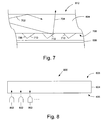
- FIG. 7 is a partial cross-sectional diagram of the LCD backlighting apparatus of FIG. 6 .
- FIG. 8 is a diagram of an LCD backlighting apparatus in accordance with an alternative embodiment of the invention.
- FIG. 9 is a process flow diagram of a method for emitting output light from a light emitting device in accordance with an embodiment of the invention.
- a light emitting diode (LED) 100 in accordance with an embodiment of the invention is described.
- the LED 100 is designed to produce “white” color output light having a high color-rendering index.
- the LED 100 is a surface mount LED.
- the LED 100 may be a different type of LED, such as a leadframe-mounted LED.
- the LED 100 includes LED dies 102 and 104 , an optional submount 106 , a mounting structure 108 and an encapsulant 110 .
- the LED dies 102 and 104 are light sources for the LED 100 .
- the LED dies 102 and 104 are semiconductor chips that generate light having a particular peak wavelength.
- the LED die 102 is configured to generate light having a peak wavelength in the blue wavelength range of the visible spectrum, which is approximately 420 nm to 490 nm. This blue light is illustrated in FIG. 1 by the arrows 112 .
- the LED die 104 is configured to generate light having a peak wavelength in the red wavelength range of the visible spectrum, which is approximately 620 nm to 800 nm. This red light is illustrated in FIG. 1 by the arrows 114 .
- the LED dies 102 and 104 are attached to the optional submount 106 , which is attached to the mounting structure 108 .
- the LED dies 102 and 104 may be directly attached to the mounting structure 108 .
- the LED dies 102 and 104 may be attached to the submount 106 or the mounting structure 108 using an electrically conductive and adhesive material, such as solder 116 .
- the submount 106 provides a thermal conductive path from the LED dies 102 and 104 to the mounting structure 108 to dissipate thermal energy from the LED dies.
- the submount 106 also provides a thermal expansion buffer between the LED dies 102 and 104 and the mounting structure 108 .
- the LED 100 is shown in FIG.
- the LED 100 may include a submount for each of the LED dies 102 and 104 .
- the mounting structure 108 includes leadframes 118 , which provide the electrical power needed to drive the LED dies 102 and 104 .
- the LED dies 102 and 104 are encapsulated in the encapsulant 110 , which is a medium for the propagation of light from the LED dies.
- the encapsulant 110 can be made of any transparent substance.
- the encapsulant 110 can be made of epoxy, silicone, a hybrid of silicone and epoxy, amorphous polyamide resin or fluorocarbon, glass and/or plastic material.
- the encapsulant 110 also contains a photoluminescent material 120 , which has a property to absorb at least some of the blue light emitted from the LED die 102 and produce longer wavelength light, such as light having a peak wavelength in the green wavelength range of the visible spectrum, which is approximately 520 nm to 565 nm.
- the photoluminescent material 120 converts some of the blue light from the LED die 102 into green light.
- This green light is illustrated in FIG. 1 by the arrows 122 .
- white light is produced by the mixing of the blue light emitted from a blue-emitting LED die and phosphor-converted green light.
- white light is typically deficient in the red wavelength region of the visible spectrum.
- this red deficiency is resolved by the inclusion of the LED die 104 , which emits red light that mixes with the original blue light from the LED die 102 and the converted green light to produce white light having a high color-rendering index.
- the photoluminescent material 120 in the encapsulant 110 may include phosphors, quantum dots, nano-phosphors, laser dyes, inorganic dyes or organic dyes. Nano-phosphors have similar optical properties as conventional phosphors. However, nano-phosphors are smaller in size than conventional phosphors, but larger than quantum dots. The size of conventional phosphors is in the range of 1-50 microns (typically in the 1-20 micron range). The size of nano-phosphors is smaller than 1 micron, but larger than quantum dots, which may be a few nanometers in size. As an example, the photoluminescent material 120 may include YAG:Ce phosphors.
- the photoluminescent material 120 is distributed throughout the encapsulant 110 .
- the entire encapsulant 120 functions as a wavelength-shifting region for the blue light emitted from the LED die 102 .
- only a portion of the encapsulant 110 may include the photoluminescent material 120 .
- a portion 224 of the encapsulant 100 over the LED die 102 includes the photoluminescent material 120 .
- the wavelength-shifting region 224 may be a thin layer covering the LED die 102 , or a layer at the upper surface of the encapsulant 110 or at some distance from the LED die 102 .
- the LED 100 is shown in FIGS. 1 and 2 as being a surface mount LED without a reflector cup. However, the LED 100 may be configured as a surface mount LED with a reflector cup. As an example, a surface mount LED 300 in accordance with an embodiment of the invention is shown in FIG. 3 . The same reference numerals used in FIGS. 1 and 2 are used to identify similar elements in FIG. 3 .
- the LED 300 includes the LED dies 102 and 104 , the optional submount 106 , the mounting structure 108 and the encapsulant 110 .
- the LED 300 further includes a reflector cup 326 formed on a poly(p-phenyleneacetylene) (PPA) housing 328 or a printed circuit board (not shown).
- PPA poly(p-phenyleneacetylene)
- the entire encapsulant 110 is a wavelength-shifting region. However, in other embodiments, a portion of the encapsulant 110 may be a wavelength-shifting region, as illustrated in FIG. 2
- the LED dies 102 and 104 of the LEDs 100 and 300 of FIGS. 1 , 2 and 3 may be stacked on top of each other, rather than being positioned side-by-side.
- FIG. 4 an LED 400 with stacked LED dies in accordance with an embodiment of the invention is shown. The same reference numerals used in FIGS. 1 , 2 and 3 are used to identify similar elements in FIG. 4 .
- the LED die 102 is stacked on top of the LED die 104 , which is attached to the optional submount 106 or directly attached to the mounting structure 108 .
- the LED dies 102 and 104 are positioned in a stacked arrangement.
- the LED die 102 is attached to the LED die 104 using an adhesive material 428 , which is electrically conductive.
- the LED die 104 is electrically connected to a leadframe 118 of the supporting structure 108 using an adhesive material 430 , which is also electrically conductive.
- the LED die 104 is also electrically connected to another leadframe 118 of the supporting structure 108 via a bond wire 431 so that driving current can be conducted through the stacked LED dies 102 and 104 .
- the LED die 104 may be stacked on top of the LED die 102 , which may be attached to the optional submount 106 or directly attached to the mounting structure 108 . As shown in FIG.
- the entire encapsulant 110 contains the photoluminescent material 120 , and thus, the entire encapsulant is a wavelength-shifting region.
- a portion of the encapsulant 110 may be a wavelength-shifting region, as illustrated in FIG. 2 .
- the LED 400 may further include a reflector cup formed on a PPA housing or a printed circuit board, as illustrated in FIG. 3 .
- FIG. 5 an LED 500 in accordance with another embodiment of the invention is shown.
- the LED 500 includes the LED dies 102 and 104 , the optional submount 106 and the mounting structure 108 .
- the LED 500 includes an additional blue-emitting LED die 532 , which can be identical to the LED die 102 .
- the additional LED die 532 is attached to the optional submount 106 .
- the LED die 532 may be attached to a separate submount (not shown), or directly attached to the mounting structure 108 .
- the LED 500 also includes an encapsulant 534 that contains an additional photoluminescent material 536 , as well as the photoluminescent material 120 .
- the encapsulant 534 of the LED 500 includes two types of photoluminescent material.
- the photoluminescent material 536 has a property to convert at least some of the blue light emitted from the LED die 532 into light having a peak wavelength in the orange wavelength range of the visible spectrum, which is approximately 590 m to 620 nm.
- the photoluminescent material 536 may include phosphors, quantum dots, nano-phosphors, laser dyes, inorganic dyes or organic dyes.
- the photoluminescent material 536 may include phosphors based on Silicate, Garnet, Sulphide, Thiometallates, Nitride, Orthosilicate, Nitridosilicate and Selenide.
- the encapsulant 534 includes a first wavelength-shifting region 538 , which contains the photoluminescent material 536 .
- the wavelength-shifting region 538 is positioned over the LED die 532 so that at least some of the light emitted from the LED die 532 can be converted into longer wavelength “orange” light by the photoluminescent material 536 in the wavelength-shifting region 538 .
- the encapsulant 534 further includes a second wavelength-shifting region 540 , which contains the other photoluminescent material 120 .
- This wavelength-shifting region 540 is positioned over the LED die 102 so that at least some of the light emitted from the LED die 102 can be converted into longer wavelength “green” light by the photoluminescent material 120 in the wavelength-shifting region 540 .
- the remaining region 541 of the encapsulant 534 does not contain any photoluminescent material, and thus, is not a wavelength-shifting region.
- this region 541 may include a photoluminescent material, such as the photoluminescent material 120 or 536 .
- the red light emitted by the LED die 104 will be transmitted through the region 541 without being converted into longer wavelength light.
- the original red light from the LED die 104 , the original blue light from the LED dies 102 and 532 , the converted green light and the converted orange light are mixed to produce white output light having a high color rendering index.
- the LEDs 100 , 300 , 400 and 500 in accordance with different embodiments of the invention may be used as light source devices for a variety of lighting applications, for example, backlighting for an illuminated display device, such as a liquid crystal display (LCD).
- an LCD backlighting apparatus 600 in accordance with an embodiment of the invention is shown.
- the backlighting apparatus 600 includes a number of LEDs 602 , a light panel 604 and a reflector 606 .
- the LEDs 602 serve as light source devices for the backlighting apparatus 600 .
- the LEDs 602 can be any type of LEDs in accordance with an embodiment of the invention. Although only three LEDs are shown in FIG. 6 , the backlighting apparatus 600 may include any number of LEDs.
- the LEDs 602 are positioned along a side 610 of the light panel 604 .
- the output light from the LEDs 602 is transmitted into the light panel 604 through the side 610 of the light panel 604 , which faces the LEDs.
- the LEDs 602 may be positioned along more than one side of the light panel 604 .
- the light panel 604 serves to direct the LED light received at the side 610 of the light panel toward the upper surface 612 of the light panel so that illuminating light is emitted from the upper surface of the light panel in a substantially uniform manner.
- the light panel 604 is a light guide panel (also known as “light pipe panel”).
- the light panel 604 will also be referred to herein as the light guide panel.
- the light panel 604 may be any light transmitting panel that can emit illuminating light from a wide surface of the panel using light from one or more LEDs.
- the light guide panel 604 is designed such that light that is internally incident on the upper surface 612 of the light guide panel at large angles with respect to normal, as illustrated by the arrow 702 , is internally reflected, while light that is internally incident on the upper surface at smaller angles, as illustrated by the arrow 704 , is transmitted through the upper surface of the light guide panel.
- the light guide panel 604 may include a light extraction feature 706 to diffuse and scatter the light within the light guide panel so that light is emitted from the upper surface 612 of the light guide panel more uniformly.
- the light extraction feature 706 may be printed, chemical-etched or laser-etched dots on the bottom surface 708 of the light guide panel 604 .
- the light extraction feature 706 may be a microstructured lens feature, as illustrated in FIG. 7 , formed on the bottom surface 708 of the light guide panel 604 .
- the microstructured lens feature 706 includes many protrusions 710 , which may have V-shaped cross-sectional profiles, that optimize angles of reflected or refracted light so that light can be extracted more uniformly from the upper surface 612 of the light guide panel 604 .
- the reflector 606 is positioned below the light guide panel 604 .
- the reflector 606 serves to reflect light emitted out of the bottom surface 708 of the light guide panel 604 back into the light guide panel so that the light may be emitted from the upper surface 612 of the light guide panel.
- the backlighting apparatus 800 includes a number of LEDs 802 and a light panel 804 .
- the LEDs 802 are positioned below the lower surface 806 of the light panel 804 , rather than being positioned along a side of the light panel.
- light from the LEDs 802 is transmitted into the lower surface 806 of the light panel 804 and emitted out of the upper surface 808 of the light panel as illuminating light.
- the LEDs 802 of the backlighting apparatus 800 can be any type of LEDs in accordance with an embodiment of the invention.
- the light panel 804 may be a light guide panel or any other light transmitting panel.
- first light having a peak wavelength in the blue wavelength range is generated from a first light source of the light emitting device, such as a blue LED die.
- second light having a peak wavelength in the red wavelength range is generated from a second light source of the light emitting device, such as a red LED die.
- the first light is received at a wavelength-shifting region, which contains a photoluminescent material. The wavelength-shifting region is optically coupled to at least the first light source.
- the first light is converted into third light having a peak wavelength longer than the peak wavelength of the first light using the photoluminescent material contained in the wavelength-shifting region.
- the first light, the second light and the third light are emitted as components of the output light, which may be white output light.
Landscapes
- Physics & Mathematics (AREA)
- General Physics & Mathematics (AREA)
- Optics & Photonics (AREA)
- Led Device Packages (AREA)
Abstract
Description
Claims (15)
Priority Applications (4)
| Application Number | Priority Date | Filing Date | Title |
|---|---|---|---|
| US11/186,221 US7922352B2 (en) | 2005-07-21 | 2005-07-21 | Device and method for emitting output light using multiple light sources with photoluminescent material |
| TW095125246A TW200707812A (en) | 2005-07-21 | 2006-07-11 | Device and method for emitting output light using multiple light sources with photoluminescent material |
| CN2006100994690A CN1901186B (en) | 2005-07-21 | 2006-07-20 | Apparatus and method for emitting output light using multiple light sources in combination with photoluminescent materials |
| JP2006199251A JP2007036232A (en) | 2005-07-21 | 2006-07-21 | Devices and methods for emitting output light using a plurality of light sources having a photoluminescent material. |
Applications Claiming Priority (1)
| Application Number | Priority Date | Filing Date | Title |
|---|---|---|---|
| US11/186,221 US7922352B2 (en) | 2005-07-21 | 2005-07-21 | Device and method for emitting output light using multiple light sources with photoluminescent material |
Publications (2)
| Publication Number | Publication Date |
|---|---|
| US20070018558A1 US20070018558A1 (en) | 2007-01-25 |
| US7922352B2 true US7922352B2 (en) | 2011-04-12 |
Family
ID=37657000
Family Applications (1)
| Application Number | Title | Priority Date | Filing Date |
|---|---|---|---|
| US11/186,221 Expired - Fee Related US7922352B2 (en) | 2005-07-21 | 2005-07-21 | Device and method for emitting output light using multiple light sources with photoluminescent material |
Country Status (4)
| Country | Link |
|---|---|
| US (1) | US7922352B2 (en) |
| JP (1) | JP2007036232A (en) |
| CN (1) | CN1901186B (en) |
| TW (1) | TW200707812A (en) |
Cited By (5)
| Publication number | Priority date | Publication date | Assignee | Title |
|---|---|---|---|---|
| US20080048193A1 (en) * | 2006-08-25 | 2008-02-28 | Samsung Electro-Mechanics Co., Ltd. | White light emitting diode module |
| US20110286201A1 (en) * | 2007-07-18 | 2011-11-24 | Chien-Yuan Wang | Wavelength converting system |
| US20140353694A1 (en) * | 2013-05-29 | 2014-12-04 | Cree Huizhou Solid State Lighting Company Limited | Multiple pixel surface mount device package |
| US11004834B2 (en) * | 2017-02-09 | 2021-05-11 | Osram Oled Gmbh | LED unit |
| US11637219B2 (en) | 2019-04-12 | 2023-04-25 | Google Llc | Monolithic integration of different light emitting structures on a same substrate |
Families Citing this family (56)
| Publication number | Priority date | Publication date | Assignee | Title |
|---|---|---|---|---|
| US9951438B2 (en) | 2006-03-07 | 2018-04-24 | Samsung Electronics Co., Ltd. | Compositions, optical component, system including an optical component, devices, and other products |
| US7736020B2 (en) * | 2006-06-16 | 2010-06-15 | Avago Technologies General Ip (Singapore) Pte. Ltd. | Illumination device and method of making the device |
| US7708427B2 (en) * | 2006-06-16 | 2010-05-04 | Avago Technologies General Ip (Singapore) Pte. Ltd. | Light source device and method of making the device |
| TWI321857B (en) * | 2006-07-21 | 2010-03-11 | Epistar Corp | A light emitting device |
| US8318407B2 (en) | 2006-11-01 | 2012-11-27 | State Of Oregon Acting By And Through The State Board Of Higher Education On Behalf Of Oregon State University | Solution processed thin films and laminates, devices comprising such thin films and laminates, and method for their use and manufacture |
| JP2010525555A (en) * | 2007-03-08 | 2010-07-22 | スリーエム イノベイティブ プロパティズ カンパニー | Array of light emitting elements |
| KR100801621B1 (en) * | 2007-06-05 | 2008-02-11 | 서울반도체 주식회사 | LED Package |
| WO2009014590A2 (en) | 2007-06-25 | 2009-01-29 | Qd Vision, Inc. | Compositions and methods including depositing nanomaterial |
| WO2009014707A2 (en) | 2007-07-23 | 2009-01-29 | Qd Vision, Inc. | Quantum dot light enhancement substrate and lighting device including same |
| US8128249B2 (en) * | 2007-08-28 | 2012-03-06 | Qd Vision, Inc. | Apparatus for selectively backlighting a material |
| TWI331397B (en) * | 2007-09-03 | 2010-10-01 | Ledtech Electronics Corp | Array type light-emitting device with high color rendering index |
| KR100982986B1 (en) * | 2008-04-17 | 2010-09-17 | 삼성엘이디 주식회사 | Submount, LED Package and Manufacturing Method Thereof |
| JP2011524064A (en) | 2008-05-06 | 2011-08-25 | キユーデイー・ビジヨン・インコーポレーテツド | Solid state lighting device containing quantum confined semiconductor nanoparticles |
| US9207385B2 (en) | 2008-05-06 | 2015-12-08 | Qd Vision, Inc. | Lighting systems and devices including same |
| WO2009137053A1 (en) | 2008-05-06 | 2009-11-12 | Qd Vision, Inc. | Optical components, systems including an optical component, and devices |
| US8021008B2 (en) * | 2008-05-27 | 2011-09-20 | Abl Ip Holding Llc | Solid state lighting using quantum dots in a liquid |
| JP2012511240A (en) * | 2008-12-04 | 2012-05-17 | ザ リージェンツ オブ ザ ユニバーシティ オブ カリフォルニア | Electroluminescence method and device using anode with nanostructured semiconductor material for electron injection |
| WO2011020098A1 (en) | 2009-08-14 | 2011-02-17 | Qd Vision, Inc. | Lighting devices, an optical component for a lighting device, and methods |
| DE202010004777U1 (en) * | 2010-04-09 | 2011-09-02 | Zumtobel Lighting Gmbh | Arrangement for emitting light with a plurality of light sources and a transparent light-emitting element |
| US8320418B2 (en) * | 2010-05-18 | 2012-11-27 | Corning Incorporated | Multiple wavelength optical systems |
| US8294168B2 (en) * | 2010-06-04 | 2012-10-23 | Samsung Electronics Co., Ltd. | Light source module using quantum dots, backlight unit employing the light source module, display apparatus, and illumination apparatus |
| KR101718066B1 (en) * | 2010-06-04 | 2017-03-20 | 삼성전자 주식회사 | light source module using quantum dot, backlight unit employing the light source module, display apparatus, and illumination apparatus |
| US8735791B2 (en) | 2010-07-13 | 2014-05-27 | Svv Technology Innovations, Inc. | Light harvesting system employing microstructures for efficient light trapping |
| US8198803B2 (en) * | 2010-07-30 | 2012-06-12 | Everlight Electronics Co., Ltd. | Color-temperature-tunable device |
| US9647162B2 (en) | 2011-01-20 | 2017-05-09 | Colossus EPC Inc. | Electronic power cell memory back-up battery |
| US20120186627A1 (en) * | 2011-01-20 | 2012-07-26 | Colossus EPC, Inc. | Electronic power source |
| US20120187763A1 (en) * | 2011-01-25 | 2012-07-26 | Isoline Component Company, Llc | Electronic power supply |
| US9097826B2 (en) | 2011-10-08 | 2015-08-04 | Svv Technology Innovations, Inc. | Collimating illumination systems employing a waveguide |
| CN102645827B (en) * | 2011-11-16 | 2014-11-05 | 深圳市光峰光电技术有限公司 | Light source system and projecting apparatus |
| CN102645829B (en) * | 2011-12-02 | 2014-11-05 | 深圳市光峰光电技术有限公司 | Light source system and projecting device |
| CN104160212B (en) * | 2012-03-01 | 2018-10-12 | 飞利浦灯具控股公司 | LED illumination is arranged |
| US9929325B2 (en) | 2012-06-05 | 2018-03-27 | Samsung Electronics Co., Ltd. | Lighting device including quantum dots |
| DE102012219460A1 (en) * | 2012-10-24 | 2014-04-24 | Osram Gmbh | LEDS MODULE |
| TWI458139B (en) * | 2012-11-23 | 2014-10-21 | 東貝光電科技股份有限公司 | White light emitting diode module |
| JP6192377B2 (en) * | 2013-06-18 | 2017-09-06 | ローム株式会社 | LED light source module |
| TWI523277B (en) * | 2013-07-12 | 2016-02-21 | 葳天科技股份有限公司 | White light emitting diode module with ultraviolet light |
| JP2015177019A (en) * | 2014-03-14 | 2015-10-05 | シチズン電子株式会社 | LED light emitting device |
| DE102015109386A1 (en) * | 2014-07-02 | 2016-01-07 | Ford Global Technologies, Llc | Photoluminescent engine compartment lighting |
| RU2696073C2 (en) * | 2015-01-13 | 2019-07-30 | ФОРД ГЛОУБАЛ ТЕКНОЛОДЖИЗ, ЭлЭлСи | Vehicle lighting system with improved substrate |
| MX2016005823A (en) * | 2015-05-12 | 2016-11-11 | Ford Global Tech Llc | SEALED LUMINISCENT FOR VEHICLE. |
| DE102016108578A1 (en) * | 2015-05-21 | 2016-11-24 | Ford Global Technologies, Llc | LUMINESCENT SEATING |
| US11112653B2 (en) * | 2015-05-29 | 2021-09-07 | Harman International Industries, Incorporated | Wide color-gamut vehicle infotainment display system with quantum dot element |
| KR102509081B1 (en) | 2015-05-29 | 2023-03-10 | 하만인터내셔날인더스트리스인코포레이티드 | High color gamut vehicle infotainment display system |
| US10656465B2 (en) | 2015-05-29 | 2020-05-19 | Harman International Industries, Incorporated | Wide color-gamut vehicle infotainment display system with quantum dot element |
| CN108139535B (en) * | 2015-10-20 | 2020-09-18 | 昕诺飞控股有限公司 | Lighting device, for example for spot lighting applications |
| WO2020048153A1 (en) * | 2018-09-04 | 2020-03-12 | 深圳市绎立锐光科技开发有限公司 | Light-emitting device |
| US10813612B2 (en) | 2019-01-25 | 2020-10-27 | Cleerly, Inc. | Systems and method of characterizing high risk plaques |
| JP7341740B2 (en) * | 2019-06-12 | 2023-09-11 | キヤノン株式会社 | Light source device and image projection device |
| US11969280B2 (en) | 2020-01-07 | 2024-04-30 | Cleerly, Inc. | Systems, methods, and devices for medical image analysis, diagnosis, risk stratification, decision making and/or disease tracking |
| KR20220124217A (en) | 2020-01-07 | 2022-09-13 | 클리어리, 인크. | Systems, methods and devices for medical image analysis, diagnosis, risk stratification, decision-making and/or disease tracking |
| US20220392065A1 (en) | 2020-01-07 | 2022-12-08 | Cleerly, Inc. | Systems, methods, and devices for medical image analysis, diagnosis, risk stratification, decision making and/or disease tracking |
| JP7212282B2 (en) | 2020-11-26 | 2023-01-25 | 日亜化学工業株式会社 | Light-emitting device and manufacturing method thereof |
| US20250217981A1 (en) | 2022-03-10 | 2025-07-03 | Cleerly, Inc. | Systems, methods, and devices for image-based plaque analysis and risk determination |
| US20250143657A1 (en) | 2022-03-10 | 2025-05-08 | Cleerly, Inc. | Systems, devices, and methods for non-invasive image-based plaque analysis and risk determination |
| US12406365B2 (en) | 2022-03-10 | 2025-09-02 | Cleerly, Inc. | Systems, devices, and methods for non-invasive image-based plaque analysis and risk determination |
| US12440180B2 (en) | 2022-03-10 | 2025-10-14 | Cleerly, Inc. | Systems, devices, and methods for non-invasive image-based plaque analysis and risk determination |
Citations (10)
| Publication number | Priority date | Publication date | Assignee | Title |
|---|---|---|---|---|
| JPS5641669A (en) * | 1979-09-11 | 1981-04-18 | Matsushita Electronics Corp | Fluorescent lamp |
| US5748161A (en) * | 1996-03-04 | 1998-05-05 | Motorola, Inc. | Integrated electro-optical package with independent menu bar |
| US5836676A (en) * | 1996-05-07 | 1998-11-17 | Koha Co., Ltd. | Light emitting display apparatus |
| US5874803A (en) * | 1997-09-09 | 1999-02-23 | The Trustees Of Princeton University | Light emitting device with stack of OLEDS and phosphor downconverter |
| US6219364B1 (en) * | 1997-01-09 | 2001-04-17 | Nec Corporation | Semiconductor laser module having improved metal substrate on peltier element |
| US6345903B1 (en) * | 2000-09-01 | 2002-02-12 | Citizen Electronics Co., Ltd. | Surface-mount type emitting diode and method of manufacturing same |
| US6351069B1 (en) | 1999-02-18 | 2002-02-26 | Lumileds Lighting, U.S., Llc | Red-deficiency-compensating phosphor LED |
| US20040012027A1 (en) * | 2002-06-13 | 2004-01-22 | Cree Lighting Company | Saturated phosphor solid state emitter |
| US20040262617A1 (en) * | 2003-06-24 | 2004-12-30 | Hahm Hun Joo | White light emitting diode and method for manufacturing the same |
| US7554257B2 (en) * | 2005-03-02 | 2009-06-30 | Osram Opto Semiconductors Gmbh | Method to generate high efficient devices which emit high quality light for illumination |
Family Cites Families (5)
| Publication number | Priority date | Publication date | Assignee | Title |
|---|---|---|---|---|
| US6513949B1 (en) * | 1999-12-02 | 2003-02-04 | Koninklijke Philips Electronics N.V. | LED/phosphor-LED hybrid lighting systems |
| JP2002057376A (en) * | 2000-05-31 | 2002-02-22 | Matsushita Electric Ind Co Ltd | LED lamp |
| JP2004055772A (en) * | 2002-07-18 | 2004-02-19 | Citizen Electronics Co Ltd | LED light emitting device |
| CN1610134A (en) * | 2003-10-23 | 2005-04-27 | 郑子淇 | light emitting device |
| CN1630107A (en) * | 2003-12-18 | 2005-06-22 | 郑子淇 | light emitting device |
-
2005
- 2005-07-21 US US11/186,221 patent/US7922352B2/en not_active Expired - Fee Related
-
2006
- 2006-07-11 TW TW095125246A patent/TW200707812A/en unknown
- 2006-07-20 CN CN2006100994690A patent/CN1901186B/en not_active Expired - Fee Related
- 2006-07-21 JP JP2006199251A patent/JP2007036232A/en active Pending
Patent Citations (10)
| Publication number | Priority date | Publication date | Assignee | Title |
|---|---|---|---|---|
| JPS5641669A (en) * | 1979-09-11 | 1981-04-18 | Matsushita Electronics Corp | Fluorescent lamp |
| US5748161A (en) * | 1996-03-04 | 1998-05-05 | Motorola, Inc. | Integrated electro-optical package with independent menu bar |
| US5836676A (en) * | 1996-05-07 | 1998-11-17 | Koha Co., Ltd. | Light emitting display apparatus |
| US6219364B1 (en) * | 1997-01-09 | 2001-04-17 | Nec Corporation | Semiconductor laser module having improved metal substrate on peltier element |
| US5874803A (en) * | 1997-09-09 | 1999-02-23 | The Trustees Of Princeton University | Light emitting device with stack of OLEDS and phosphor downconverter |
| US6351069B1 (en) | 1999-02-18 | 2002-02-26 | Lumileds Lighting, U.S., Llc | Red-deficiency-compensating phosphor LED |
| US6345903B1 (en) * | 2000-09-01 | 2002-02-12 | Citizen Electronics Co., Ltd. | Surface-mount type emitting diode and method of manufacturing same |
| US20040012027A1 (en) * | 2002-06-13 | 2004-01-22 | Cree Lighting Company | Saturated phosphor solid state emitter |
| US20040262617A1 (en) * | 2003-06-24 | 2004-12-30 | Hahm Hun Joo | White light emitting diode and method for manufacturing the same |
| US7554257B2 (en) * | 2005-03-02 | 2009-06-30 | Osram Opto Semiconductors Gmbh | Method to generate high efficient devices which emit high quality light for illumination |
Cited By (9)
| Publication number | Priority date | Publication date | Assignee | Title |
|---|---|---|---|---|
| US20080048193A1 (en) * | 2006-08-25 | 2008-02-28 | Samsung Electro-Mechanics Co., Ltd. | White light emitting diode module |
| US20080197366A1 (en) * | 2006-08-25 | 2008-08-21 | Samsung Electro-Mechanics Co., Ltd. | White light emitting diode module |
| US20110286201A1 (en) * | 2007-07-18 | 2011-11-24 | Chien-Yuan Wang | Wavelength converting system |
| US8210699B2 (en) * | 2007-07-18 | 2012-07-03 | Epistar Corporation | Wavelength converting system |
| US20140353694A1 (en) * | 2013-05-29 | 2014-12-04 | Cree Huizhou Solid State Lighting Company Limited | Multiple pixel surface mount device package |
| US9711489B2 (en) * | 2013-05-29 | 2017-07-18 | Cree Huizhou Solid State Lighting Company Limited | Multiple pixel surface mount device package |
| US11004834B2 (en) * | 2017-02-09 | 2021-05-11 | Osram Oled Gmbh | LED unit |
| US11637219B2 (en) | 2019-04-12 | 2023-04-25 | Google Llc | Monolithic integration of different light emitting structures on a same substrate |
| US12191418B2 (en) | 2019-04-12 | 2025-01-07 | Google Llc | Monolithic integration of different light emitting structures on a same substrate |
Also Published As
| Publication number | Publication date |
|---|---|
| TW200707812A (en) | 2007-02-16 |
| CN1901186A (en) | 2007-01-24 |
| JP2007036232A (en) | 2007-02-08 |
| US20070018558A1 (en) | 2007-01-25 |
| CN1901186B (en) | 2010-05-12 |
Similar Documents
| Publication | Publication Date | Title |
|---|---|---|
| US7922352B2 (en) | Device and method for emitting output light using multiple light sources with photoluminescent material | |
| KR100930171B1 (en) | White light emitting device and white light source module using same | |
| US8648371B2 (en) | LED unit having electrochromic element | |
| US20110089815A1 (en) | Light-emitting device | |
| KR100771811B1 (en) | White light emitting device | |
| KR20110048397A (en) | LED package and backlight unit using the same | |
| KR20150113183A (en) | Light-emitting module | |
| US20060038198A1 (en) | Device and method for producing output light having a wavelength spectrum in the visible range and the infrared range using a fluorescent material | |
| US8040039B2 (en) | Device and method for emitting composite output light using multiple wavelength-conversion mechanisms | |
| CN1921106B (en) | Optoelectronic package and manufacture, method and system using same | |
| KR20040088418A (en) | Tri-color white light emitted diode | |
| KR20100076655A (en) | White light emitting device | |
| KR101724699B1 (en) | Light emitting apparatus and lighting system | |
| KR20100065253A (en) | White light emitting device and white light source module using the same | |
| KR101456267B1 (en) | Lighting device | |
| CN2938405Y (en) | Led | |
| KR100712880B1 (en) | White light emitting diodes can reduce color temperature variations | |
| KR102019501B1 (en) | Phosphor and light emitting device having thereof | |
| KR100990647B1 (en) | White light emitting device and white light source module using same | |
| US7737635B2 (en) | High efficiency white light emitting diode and method for manufacturing the same | |
| KR20080041818A (en) | Lens and light emitting device package including the same | |
| US20070075346A1 (en) | Light emitting diode and the package structure thereof | |
| KR20130027653A (en) | Led white light source module | |
| KR100820538B1 (en) | Light emitting device and image display device having same | |
| KR20170133824A (en) | Phosphor composition, light emitting device package and lighting apparatus |
Legal Events
| Date | Code | Title | Description |
|---|---|---|---|
| AS | Assignment |
Owner name: AGILENT TECHNOLOGIES INC., COLORADO Free format text: ASSIGNMENT OF ASSIGNORS INTEREST;ASSIGNORS:CHUA, JANET BEE YIN;LAU, YUE HOONG;REEL/FRAME:016473/0178 Effective date: 20050706 |
|
| AS | Assignment |
Owner name: AVAGO TECHNOLOGIES GENERAL IP PTE. LTD.,SINGAPORE Free format text: ASSIGNMENT OF ASSIGNORS INTEREST;ASSIGNOR:AGILENT TECHNOLOGIES, INC.;REEL/FRAME:017206/0666 Effective date: 20051201 Owner name: AVAGO TECHNOLOGIES GENERAL IP PTE. LTD., SINGAPORE Free format text: ASSIGNMENT OF ASSIGNORS INTEREST;ASSIGNOR:AGILENT TECHNOLOGIES, INC.;REEL/FRAME:017206/0666 Effective date: 20051201 |
|
| STCF | Information on status: patent grant |
Free format text: PATENTED CASE |
|
| AS | Assignment |
Owner name: DEUTSCHE BANK AG NEW YORK BRANCH, AS COLLATERAL AGENT, NEW YORK Free format text: PATENT SECURITY AGREEMENT;ASSIGNOR:AVAGO TECHNOLOGIES GENERAL IP (SINGAPORE) PTE. LTD.;REEL/FRAME:032851/0001 Effective date: 20140506 Owner name: DEUTSCHE BANK AG NEW YORK BRANCH, AS COLLATERAL AG Free format text: PATENT SECURITY AGREEMENT;ASSIGNOR:AVAGO TECHNOLOGIES GENERAL IP (SINGAPORE) PTE. LTD.;REEL/FRAME:032851/0001 Effective date: 20140506 |
|
| FPAY | Fee payment |
Year of fee payment: 4 |
|
| AS | Assignment |
Owner name: AVAGO TECHNOLOGIES GENERAL IP (SINGAPORE) PTE. LTD., SINGAPORE Free format text: TERMINATION AND RELEASE OF SECURITY INTEREST IN PATENT RIGHTS (RELEASES RF 032851-0001);ASSIGNOR:DEUTSCHE BANK AG NEW YORK BRANCH, AS COLLATERAL AGENT;REEL/FRAME:037689/0001 Effective date: 20160201 Owner name: AVAGO TECHNOLOGIES GENERAL IP (SINGAPORE) PTE. LTD Free format text: TERMINATION AND RELEASE OF SECURITY INTEREST IN PATENT RIGHTS (RELEASES RF 032851-0001);ASSIGNOR:DEUTSCHE BANK AG NEW YORK BRANCH, AS COLLATERAL AGENT;REEL/FRAME:037689/0001 Effective date: 20160201 |
|
| AS | Assignment |
Owner name: BANK OF AMERICA, N.A., AS COLLATERAL AGENT, NORTH CAROLINA Free format text: PATENT SECURITY AGREEMENT;ASSIGNOR:AVAGO TECHNOLOGIES GENERAL IP (SINGAPORE) PTE. LTD.;REEL/FRAME:037808/0001 Effective date: 20160201 Owner name: BANK OF AMERICA, N.A., AS COLLATERAL AGENT, NORTH Free format text: PATENT SECURITY AGREEMENT;ASSIGNOR:AVAGO TECHNOLOGIES GENERAL IP (SINGAPORE) PTE. LTD.;REEL/FRAME:037808/0001 Effective date: 20160201 |
|
| AS | Assignment |
Owner name: AVAGO TECHNOLOGIES GENERAL IP (SINGAPORE) PTE. LTD., SINGAPORE Free format text: CORRECTIVE ASSIGNMENT TO CORRECT THE ASSIGNEE NAME PREVIOUSLY RECORDED AT REEL: 017206 FRAME: 0666. ASSIGNOR(S) HEREBY CONFIRMS THE ASSIGNMENT;ASSIGNOR:AGILENT TECHNOLOGIES, INC.;REEL/FRAME:038632/0662 Effective date: 20051201 Owner name: AVAGO TECHNOLOGIES GENERAL IP (SINGAPORE) PTE. LTD Free format text: CORRECTIVE ASSIGNMENT TO CORRECT THE ASSIGNEE NAME PREVIOUSLY RECORDED AT REEL: 017206 FRAME: 0666. ASSIGNOR(S) HEREBY CONFIRMS THE ASSIGNMENT;ASSIGNOR:AGILENT TECHNOLOGIES, INC.;REEL/FRAME:038632/0662 Effective date: 20051201 |
|
| AS | Assignment |
Owner name: AVAGO TECHNOLOGIES GENERAL IP (SINGAPORE) PTE. LTD., SINGAPORE Free format text: TERMINATION AND RELEASE OF SECURITY INTEREST IN PATENTS;ASSIGNOR:BANK OF AMERICA, N.A., AS COLLATERAL AGENT;REEL/FRAME:041710/0001 Effective date: 20170119 Owner name: AVAGO TECHNOLOGIES GENERAL IP (SINGAPORE) PTE. LTD Free format text: TERMINATION AND RELEASE OF SECURITY INTEREST IN PATENTS;ASSIGNOR:BANK OF AMERICA, N.A., AS COLLATERAL AGENT;REEL/FRAME:041710/0001 Effective date: 20170119 |
|
| MAFP | Maintenance fee payment |
Free format text: PAYMENT OF MAINTENANCE FEE, 8TH YEAR, LARGE ENTITY (ORIGINAL EVENT CODE: M1552); ENTITY STATUS OF PATENT OWNER: LARGE ENTITY Year of fee payment: 8 |
|
| AS | Assignment |
Owner name: AVAGO TECHNOLOGIES INTERNATIONAL SALES PTE. LIMITED, SINGAPORE Free format text: MERGER;ASSIGNOR:AVAGO TECHNOLOGIES GENERAL IP (SINGAPORE) PTE. LTD.;REEL/FRAME:047196/0687 Effective date: 20180509 Owner name: AVAGO TECHNOLOGIES INTERNATIONAL SALES PTE. LIMITE Free format text: MERGER;ASSIGNOR:AVAGO TECHNOLOGIES GENERAL IP (SINGAPORE) PTE. LTD.;REEL/FRAME:047196/0687 Effective date: 20180509 |
|
| AS | Assignment |
Owner name: AVAGO TECHNOLOGIES INTERNATIONAL SALES PTE. LIMITED, SINGAPORE Free format text: CORRECTIVE ASSIGNMENT TO CORRECT THE EFFECTIVE DATE OF MERGER TO 9/5/2018 PREVIOUSLY RECORDED AT REEL: 047196 FRAME: 0687. ASSIGNOR(S) HEREBY CONFIRMS THE MERGER;ASSIGNOR:AVAGO TECHNOLOGIES GENERAL IP (SINGAPORE) PTE. LTD.;REEL/FRAME:047630/0344 Effective date: 20180905 Owner name: AVAGO TECHNOLOGIES INTERNATIONAL SALES PTE. LIMITE Free format text: CORRECTIVE ASSIGNMENT TO CORRECT THE EFFECTIVE DATE OF MERGER TO 9/5/2018 PREVIOUSLY RECORDED AT REEL: 047196 FRAME: 0687. ASSIGNOR(S) HEREBY CONFIRMS THE MERGER;ASSIGNOR:AVAGO TECHNOLOGIES GENERAL IP (SINGAPORE) PTE. LTD.;REEL/FRAME:047630/0344 Effective date: 20180905 |
|
| AS | Assignment |
Owner name: AVAGO TECHNOLOGIES INTERNATIONAL SALES PTE. LIMITE Free format text: CORRECTIVE ASSIGNMENT TO CORRECT THE PROPERTY NUMBERS PREVIOUSLY RECORDED AT REEL: 47630 FRAME: 344. ASSIGNOR(S) HEREBY CONFIRMS THE ASSIGNMENT;ASSIGNOR:AVAGO TECHNOLOGIES GENERAL IP (SINGAPORE) PTE. LTD.;REEL/FRAME:048883/0267 Effective date: 20180905 Owner name: AVAGO TECHNOLOGIES INTERNATIONAL SALES PTE. LIMITED, SINGAPORE Free format text: CORRECTIVE ASSIGNMENT TO CORRECT THE PROPERTY NUMBERS PREVIOUSLY RECORDED AT REEL: 47630 FRAME: 344. ASSIGNOR(S) HEREBY CONFIRMS THE ASSIGNMENT;ASSIGNOR:AVAGO TECHNOLOGIES GENERAL IP (SINGAPORE) PTE. LTD.;REEL/FRAME:048883/0267 Effective date: 20180905 |
|
| FEPP | Fee payment procedure |
Free format text: MAINTENANCE FEE REMINDER MAILED (ORIGINAL EVENT CODE: REM.); ENTITY STATUS OF PATENT OWNER: LARGE ENTITY |
|
| LAPS | Lapse for failure to pay maintenance fees |
Free format text: PATENT EXPIRED FOR FAILURE TO PAY MAINTENANCE FEES (ORIGINAL EVENT CODE: EXP.); ENTITY STATUS OF PATENT OWNER: LARGE ENTITY |
|
| STCH | Information on status: patent discontinuation |
Free format text: PATENT EXPIRED DUE TO NONPAYMENT OF MAINTENANCE FEES UNDER 37 CFR 1.362 |
|
| FP | Lapsed due to failure to pay maintenance fee |
Effective date: 20230412 |