US7826055B2 - Optical channel analyzer with variable filter - Google Patents
Optical channel analyzer with variable filter Download PDFInfo
- Publication number
- US7826055B2 US7826055B2 US11/716,238 US71623807A US7826055B2 US 7826055 B2 US7826055 B2 US 7826055B2 US 71623807 A US71623807 A US 71623807A US 7826055 B2 US7826055 B2 US 7826055B2
- Authority
- US
- United States
- Prior art keywords
- optical
- filter
- analyzer
- optical beam
- area
- Prior art date
- Legal status (The legal status is an assumption and is not a legal conclusion. Google has not performed a legal analysis and makes no representation as to the accuracy of the status listed.)
- Expired - Fee Related, expires
Links
- 230000003287 optical effect Effects 0.000 title claims abstract description 485
- 238000010183 spectrum analysis Methods 0.000 claims abstract description 18
- 238000004891 communication Methods 0.000 claims description 16
- 230000003595 spectral effect Effects 0.000 claims description 15
- 230000033001 locomotion Effects 0.000 claims description 13
- 239000013307 optical fiber Substances 0.000 claims description 13
- 238000013461 design Methods 0.000 description 19
- 238000000034 method Methods 0.000 description 11
- MROJXXOCABQVEF-UHFFFAOYSA-N Actarit Chemical compound CC(=O)NC1=CC=C(CC(O)=O)C=C1 MROJXXOCABQVEF-UHFFFAOYSA-N 0.000 description 10
- 239000000835 fiber Substances 0.000 description 9
- 230000005540 biological transmission Effects 0.000 description 5
- 239000011248 coating agent Substances 0.000 description 5
- 238000000576 coating method Methods 0.000 description 5
- 238000012544 monitoring process Methods 0.000 description 5
- 238000004519 manufacturing process Methods 0.000 description 4
- 238000004611 spectroscopical analysis Methods 0.000 description 4
- 238000012360 testing method Methods 0.000 description 4
- 238000002834 transmittance Methods 0.000 description 3
- 238000004458 analytical method Methods 0.000 description 2
- 230000008901 benefit Effects 0.000 description 2
- 230000007423 decrease Effects 0.000 description 2
- 238000000151 deposition Methods 0.000 description 2
- 239000000463 material Substances 0.000 description 2
- 238000001228 spectrum Methods 0.000 description 2
- 239000000758 substrate Substances 0.000 description 2
- 241000016649 Copaifera officinalis Species 0.000 description 1
- 239000004859 Copal Substances 0.000 description 1
- 238000004566 IR spectroscopy Methods 0.000 description 1
- 238000001069 Raman spectroscopy Methods 0.000 description 1
- 238000004847 absorption spectroscopy Methods 0.000 description 1
- BJQHLKABXJIVAM-UHFFFAOYSA-N bis(2-ethylhexyl) phthalate Chemical compound CCCCC(CC)COC(=O)C1=CC=CC=C1C(=O)OCC(CC)CCCC BJQHLKABXJIVAM-UHFFFAOYSA-N 0.000 description 1
- 238000010276 construction Methods 0.000 description 1
- 239000003989 dielectric material Substances 0.000 description 1
- 238000009826 distribution Methods 0.000 description 1
- 230000000694 effects Effects 0.000 description 1
- 238000004993 emission spectroscopy Methods 0.000 description 1
- 230000008020 evaporation Effects 0.000 description 1
- 238000001704 evaporation Methods 0.000 description 1
- 238000001506 fluorescence spectroscopy Methods 0.000 description 1
- 238000001659 ion-beam spectroscopy Methods 0.000 description 1
- 238000001755 magnetron sputter deposition Methods 0.000 description 1
- 230000000873 masking effect Effects 0.000 description 1
- 238000005259 measurement Methods 0.000 description 1
- 238000005240 physical vapour deposition Methods 0.000 description 1
- 230000010287 polarization Effects 0.000 description 1
- 238000012545 processing Methods 0.000 description 1
- 239000000126 substance Substances 0.000 description 1
- 230000007704 transition Effects 0.000 description 1
- 238000001771 vacuum deposition Methods 0.000 description 1
Images


Classifications
-
- G—PHYSICS
- G01—MEASURING; TESTING
- G01J—MEASUREMENT OF INTENSITY, VELOCITY, SPECTRAL CONTENT, POLARISATION, PHASE OR PULSE CHARACTERISTICS OF INFRARED, VISIBLE OR ULTRAVIOLET LIGHT; COLORIMETRY; RADIATION PYROMETRY
- G01J3/00—Spectrometry; Spectrophotometry; Monochromators; Measuring colours
- G01J3/28—Investigating the spectrum
- G01J3/30—Measuring the intensity of spectral lines directly on the spectrum itself
- G01J3/32—Investigating bands of a spectrum in sequence by a single detector
-
- G—PHYSICS
- G01—MEASURING; TESTING
- G01J—MEASUREMENT OF INTENSITY, VELOCITY, SPECTRAL CONTENT, POLARISATION, PHASE OR PULSE CHARACTERISTICS OF INFRARED, VISIBLE OR ULTRAVIOLET LIGHT; COLORIMETRY; RADIATION PYROMETRY
- G01J3/00—Spectrometry; Spectrophotometry; Monochromators; Measuring colours
- G01J3/12—Generating the spectrum; Monochromators
- G01J2003/1213—Filters in general, e.g. dichroic, band
- G01J2003/1217—Indexed discrete filters or choppers
-
- G—PHYSICS
- G01—MEASURING; TESTING
- G01J—MEASUREMENT OF INTENSITY, VELOCITY, SPECTRAL CONTENT, POLARISATION, PHASE OR PULSE CHARACTERISTICS OF INFRARED, VISIBLE OR ULTRAVIOLET LIGHT; COLORIMETRY; RADIATION PYROMETRY
- G01J3/00—Spectrometry; Spectrophotometry; Monochromators; Measuring colours
- G01J3/12—Generating the spectrum; Monochromators
- G01J2003/1213—Filters in general, e.g. dichroic, band
- G01J2003/1221—Mounting; Adjustment
-
- G—PHYSICS
- G01—MEASURING; TESTING
- G01J—MEASUREMENT OF INTENSITY, VELOCITY, SPECTRAL CONTENT, POLARISATION, PHASE OR PULSE CHARACTERISTICS OF INFRARED, VISIBLE OR ULTRAVIOLET LIGHT; COLORIMETRY; RADIATION PYROMETRY
- G01J3/00—Spectrometry; Spectrophotometry; Monochromators; Measuring colours
- G01J3/12—Generating the spectrum; Monochromators
- G01J2003/1226—Interference filters
- G01J2003/123—Indexed discrete filters
Definitions
- Communication networks include one or more optical fibers that carry one or more optical signals. It is often very important to monitor the optical signals to determine the wavelengths of the optical signals and/or the power of the optical signals. With this information, the communication network can be adjusted to improve the performance.
- spectroscopy involves analyzing the wavelength(s) of different types of visible and invisible light to detect the molecular content or structural information of a substance being analyzed, or for other suitable purposes known to those skilled in the art.
- Various types of spectroscopy include absorption spectroscopy (i.e. ultraviolet, visible and/or infrared spectroscopy), emission spectroscopy (i.e. fluorescence spectroscopy) and scattering spectroscopy (i.e. Raman spectroscopy), as non-exclusive examples.
- the present invention is directed to an analyzer for performing spectral analysis on a first optical beam.
- the analyzer includes an optical filter, a mover, and an optical launcher assembly.
- the optical filter includes a first filter area.
- the mover moves the optical filter.
- the optical launcher assembly directs a portion of the first optical beam at the first filter area so that the first optical beam is near normal incidence to the first filter area.
- the mover rotates the optical filter about a filter rotational axis and the optical launcher assembly directs the first optical beam at the first filter area so that the first optical beam is substantially parallel to the filter rotational axis.
- the optical launcher assembly can direct a second optical beam at the first filter area with the second optical beam at near normal incidence to the first filter area and spaced apart from the first optical beam.
- the first optical beam and the second optical beam are carrying the same optical signals.
- a fiber coupler can be used to split an optical fiber into a first fiber and a second fiber, and divide the optical signals.
- the optical launcher assembly can direct two spaced apart optical beams at the first filter area.
- the launcher assembly can include a beam splitter that causes two or more spaced apart optical beams to be directed at the optical filter. With this design, the simultaneous analysis of the same optical signals can be used to deconvolve multiple input signals.
- the first optical beam and the second optical beam can be carrying different optical signals.
- the optical analyzer can be used to simultaneously monitor multiple different optical signals.
- the optical filter can include a second filter area.
- the optical launcher assembly can direct a portion of the first optical beam or a portion of the second optical beam at the second filter area. This design can allow for the testing of different ranges of optical signals with the same optical filter.
- the filter area is a band pass type filter that includes multiple, alternative center wavelengths that are distributed along the filter area.
- the filter area can be a narrow band pass filter having a center wavelength value that varies along the filter area.
- the optical analyzer can include an optical redirector that causes a portion of the first optical beam to make two passes through the same optical filter. This improves discrimination for the optical analyzer.
- FIG. 1 is a simplified illustration of a precision apparatus having features of the present invention
- FIG. 2 is a plan view of an optical filter having features of the present invention
- FIG. 3 is a plan view of a wafer that can be used to make the optical filter of FIG. 2 ;
- FIGS. 4A and 4B are alternative, simplified illustrations of a portion of the precision apparatus of FIG. 1 ;
- FIGS. 5 , 6 , 7 , 8 and 9 are simplified illustrations of alternative embodiments of a precision apparatus
- FIGS. 10 and 11 are plan views of alternative optical filters having features of the present invention.
- FIG. 12 is simplified illustration of an additional alternative embodiment of a precision apparatus.
- FIG. 13 is a graph that illustrates the alternative center wavelengths of one embodiment of an optical filter having features of the present invention.
- FIG. 1 is a simplified view of one non-exclusive embodiment of the precision apparatus 10 .
- the precision apparatus 10 includes an optical network 12 (only a portion is illustrated in FIG. 1 ) and an optical analyzer 14 .
- the design and orientation of the components of the precision apparatus 10 can be changed to suit the requirements of the precision apparatus 10 .
- the optical analyzer 14 provides a relatively simple, low cost, relatively compact, and highly reliable device for performing spectral analysis and/or monitoring of the optical network 12 or a portion thereof. Further, in certain embodiments, the optical analyzer 14 can be used to alternatively or simultaneously monitor multiple optical signals.
- the optical network 12 includes one or more optical fibers 16 , that each carries one or more optical signals. As provided herein, for each optical fiber 16 , an optical beam 18 can be analyzed that includes the multiple optical signals. In FIG. 1 , the optical network 12 includes three optical fibers 16 . However, the optical network 12 could be designed with more than three or less than three optical fibers 16 . Additionally, the optical network 12 can include multiple other components that are not shown in FIG. 1 . For example, the optical network 12 can include one or more lasers, receivers, and amplifiers.
- the optical analyzer 14 performs spectral analysis on one or more of the optical beams 18 .
- the spectral analysis can include determining the wavelength and power level of the one or more optical signals. With this information, the operation and performance of the precision apparatus 10 can be adjusted.
- the optical analyzer 14 determines the wavelength and power level of one or more optical signals in the optical beam 18 .
- the optical analyzer 14 could be used to only determine the wavelength of the optical signals.
- the optical analyzer 14 is a channel monitor that is designed to perform spectral analysis on the communication bands.
- communication bands are at frequencies of between approximately 1526 and 1575 nanometers.
- the analyzer 14 could be designed to perform spectral analysis on beams 18 that are at wavelengths that are greater than or lesser than the communication bands.
- the optical analyzer 14 can be designed to perform spectral analysis on the L bands that are at frequencies of between approximately 1571 and 1610 nanometers.
- the design of the optical analyzer 14 can vary pursuant to the teachings provided herein.
- the optical analyzer 14 includes a filter assembly 20 , a beam detector 21 , and a control system 22 .
- the filter assembly 20 transmits or blocks a portion of the spectrum of the optical beam 18 that is directed at the filter assembly 20 . If the spectrum is narrow spectral source such as a laser, then the filter will either transmit or block the beam. The portion of the optical beam 18 that passes through the filter assembly 20 is referred to herein as the transmitted optical beam 24 . The transmitted optical beam 24 is subsequently transferred to the beam detector 21 .
- the filter assembly 20 can vary pursuant to the teachings provided herein.
- the filter assembly 20 includes a filter base 26 , an optical filter 28 , a mover 30 , an position sensor 32 , a bracket 34 , a beam launcher assembly 35 including a optical launcher 36 , a beam receiver 38 , and a beam redirector 40 .
- optical analyzer 14 is a two pass system, with the transmitted optical beam 24 having passed twice through the optical filter 28 . This can improve the discrimination and accuracy.
- the filter assembly 20 could be designed without one or more of these components.
- the filter assembly 20 could be designed without the beam redirector 40 .
- the optical analyzer 14 can be a single pass system, with the transmitted optical beam 24 passing only once through the optical filter 28 .
- the filter assembly 20 could be designed with a plurality of beam redirectors 40 that cause the optical beam 18 to pass more than two times through the optical filter 28 .
- the filter base 26 supports the other components of the filter assembly 20 .
- the filter base 26 is a rigid plate.
- the filter base 26 could have another configuration.
- the optical filter 28 filters the optical beam 18 .
- the optical filter 28 is generally disk shaped and includes a first filter side 42 that faces the optical launcher 36 and an opposed second filter side 44 that faces the optical redirector 40 .
- the first filter side 42 includes a filter area 46 that is a band pass type filter that transmits a band of wavelengths (“the passband”) and blocks wavelengths outside of the passband.
- the passband has a center wavelength that is at that the center of the passband.
- the filter area 46 has multiple different center wavelengths that are spread along the filter area 46 .
- the filter is a narrow band pass filter with a passband having a bandwidth of less than approximately 0.1, 0.2, 0.5, 1, or 5 nanometers
- the transition from transmitting to rejection can be gradual (“wide band pass filter”) or sharp (“narrow band pass filter”).
- the filter area 46 is a narrow band pass interference type filter.
- the filter area 46 is an edge filter with relatively steep spectral slopes.
- the edge filter has a spectral slope capable of transitioning between 10% and 90% transmission in less than 0.2 nm, 0.5 nm, 1 nm, or 5 nm.
- the term “steep spectral slope” shall mean a spectral slope capable of transitioning between 10% and 90% transmission in less than 0.2 nm, 0.5 nm, 1 nm, or 5 nm.
- FIG. 2 illustrates a plan view of the first filter side 42 of one embodiment of the optical filter 28 .
- the filter area 46 is generally annular disk shaped.
- the filter area 46 could have another shape.
- the value of the center wavelength varies continuously along the filter area 46 .
- the value of the center wavelength varies around the circumference of the filter area 46 .
- the filter area 46 transmits the center wavelength of approximately 1500 nm and rejects wavelengths outside the center wavelength 1500 nm;
- the filter area 46 transmits the center wavelength of approximately 1525 nm and rejects wavelengths outside the center wavelength 1525 nm;
- the filter area 46 transmits the center wavelength of approximately 1550 nm and rejects wavelengths outside the center wavelength 1550 nm;
- the filter area 46 transmits the center wavelength of approximately 1575 nm and rejects wavelengths outside the center wavelength 1575 nm.
- the center wavelength value that corresponds to 0, 90, 180, 270 degrees can have other values.
- the center wavelength can vary substantially linearly or non-linearly; (ii) for the radial positions between 90 to 180 degrees, the center wavelength can vary substantially linearly or non-linearly; (iii) for the radial positions between 180 to 270 degrees, the center wavelength can vary substantially linearly or non-linearly; and (iv) for the radial positions between 270 to 0 degrees, the center wavelength can vary substantially linearly or non-linearly.
- the filter area 46 can be made so that for every degree (e.g. radial position) from 0 and 359 degrees, the center wavelength varies (e.g. increases or decreases) approximately 0.01, 0.05, 0.1, 0.2, 0.5, 1, or 2 nanometers. However, other values can be used.
- the method used for making the optical filter 28 can vary.
- the optical filter 28 is a circular variable interference filter in which the center wavelength varies relatively linearly.
- the filter area 46 is made of four separate arch shaped segments, including a first filter segment 248 A, a second filter segment 248 B, a third filter segment 248 C, and a fourth filter segment 248 D that are secured together to form the annular disk shaped filter area 46 .
- the filter area 46 could be made with more than four or less than four filter segments 248 A- 248 D. These filter segments 248 A- 248 D can be secured to a transparent disk (not shown) or a hub (not shown).
- optical filter 28 can have another configuration other than a disk shape.
- the optical filter 28 could include one or more linear filters.
- FIG. 3 is a simplified top view of a wafer 350 that can be used to make one or more of the filter segments 248 A- 248 D.
- the wafer 350 is a substrate that has been coated with filter material so that the value of the center wavelength varies along the wafer 350 .
- the right column is a reference system that outlines a plurality of positions on the wafer 350 relative to a reference point 352 .
- the reference point 352 is at the center position of the wafer 350 .
- the reference point 352 can be located at the edge of the wafer 350 .
- the reference system is in increments of 10 mm.
- reference line 10 corresponds to a line that is 10 mm away from the reference point 352
- reference line ⁇ 10 corresponds to a line that is ⁇ 10 mm away from the reference point 352 .
- the left column in FIG. 3 references the center wavelength of the wafer 350 at that particular location.
- the left column lists the different center wavelengths A-O.
- the wafer 350 has (i) a center wavelength that is equal to A at 70 mm from the reference point 352 ; (ii) a center wavelength of B at 60 mm from the reference point 352 ; (iii) a center wavelength of C at approximately 50 mm from the reference point 352 ; (iv) a center wavelength of D at 40 mm from the reference point 352 ; (v) a center wavelength of E at 30 mm from the reference point 352 ; (vi) a center wavelength of F at 20 mm from the reference point 352 ; (vii) a center wavelength of G at 10 mm from the reference point 352 ; (viii) a center wavelength of H at the reference point 352 ; (ix) a center wavelength of I at ⁇ 10 mm from the reference point 352 ; (x) a center wavelength
- the value of the center wavelength that corresponds to A-O can be varied to suit the optical beam 18 (illustrated in FIG. 1 ) being analyzed.
- the center wavelength varies from the top to the bottom of the wafer 350 .
- the center wavelength can vary substantially linearly or non-linearly from top to bottom.
- center wavelength A has a value of approximately 1430 nanometer;
- center wavelength B has a value of approximately 1455 nanometer;
- center wavelength C has a value of approximately 1475 nanometer;
- center wavelength D has a value of approximately 1502 nanometer;
- center wavelength E has a value of approximately 1523 nanometer;
- center wavelength F has a value of approximately 1541 nanometer;
- center wavelength G has a value of approximately 1555 nanometer;
- center wavelength H has a value of approximately 1564 nanometer;
- center wavelength I has a value of approximately 1572 nanometer;
- center wavelength J has a value of approximately 1577 nanometer;
- center wavelength K has a value of approximately 1584 nanometer;
- center wavelength L has a value of approximately 1591 nanometer;
- center wavelength M has a value of approximately 1598 nanometer;
- center wavelength N has a value of approximately 1604
- center wavelength A has a value of approximately 1500 nanometer;
- center wavelength B has a value of approximately 1510 nanometer;
- center wavelength C has a value of approximately 1520 nanometer;
- center wavelength D has a value of approximately 1530 nanometer;
- center wavelength E has a value of approximately 1540 nanometer;
- center wavelength F has a value of approximately 1550 nanometer;
- center wavelength G has a value of approximately 1560 nanometer;
- center wavelength H has a value of approximately 1570 nanometer;
- center wavelength I has a value of approximately 1580 nanometer;
- center wavelength J has a value of approximately 1590 nanometer;
- center wavelength K has a value of approximately 1600 nanometer;
- center wavelength L has a value of approximately 1610 nanometer;
- center wavelength M has a value of approximately 1620 nanometer;
- center wavelength N has a value of approximately 1630 nanometer
- wavelength of A overlaps multiple arch segments. This prevents gaps in spectral coverage of the analyzer.
- the wafer 350 includes an interference coating that is deposited on the substrate in a vacuum coating chamber (not shown).
- the coating can be made up of thin layers of dielectrics, resulting in high transmission over narrow spectral bands.
- the chamber is designed to vary the center wavelength of the filter linearly across the wafer 350 in a controlled manner.
- a non-linear variation can be used.
- a non-linear variation can be used which when translated to a circular motion provides a linear change in wavelength with angle.
- the dense dielectric filter material can be deposited using a number of different methods including physical vapor deposition such as ion beam sputtering, magnetron sputtering, and ion assisted evaporation.
- physical vapor deposition such as ion beam sputtering, magnetron sputtering, and ion assisted evaporation.
- One method for depositing a coating is disclosed in U.S. Pat. No. 6,736,943, the contents of which are incorporated herein by reference.
- laser monitoring at the center wavelength of the filter can be used for accurate thickness control. This can be useful for multiple cavity bandpass designs.
- the center wavelength gradient across the filter can be created and controlled by either physical masking of the depositing vapor or careful selection of the source location to provide the required uniformity.
- the arch shaped filter segments 248 A- 248 D can be cut from the wafer 350 and assembled to form the filter area 46 (illustrated in FIG. 2 ) having the center wavelength that varies around the circumference of the filter area 46 .
- the filter segments 248 A- 248 D are slightly overlapping. Because the edges of the filter segments 248 A- 248 D overlap slightly, the assembled filter area 46 does not have a gap in the center wavelength at the intersection of the filter segments 248 A- 248 D.
- the filter segments 248 A- 248 D can be cut from other regions of the wafer 350 to achieve the desired center wavelength distribution of the filter area 46 .
- FIG. 3 illustrates that the wafer 350 can include more than four filter segments 248 A- 248 D.
- FIG. 3 illustrates seven additional filter segments 354 A-G.
- filter segments 354 A-D can be used to make another optical filter (not shown).
- the center wavelength varies substantially linearly along a line 249 A- 249 D that is substantially tangential to a center axis 247 of the filter 28 .
- arrow 249 A illustrates that the center wavelength increases linearly for filter segment 248 A substantially tangential to the center axis 247
- arrow 249 B illustrates that the center wavelength increases linearly for filter segment 248 B substantially tangential to the center axis 247
- arrow 249 C illustrates that the center wavelength increases linearly for filter segment 248 C substantially tangential to the center axis 247
- arrow 249 D illustrates that the center wavelength increases linearly for filter segment 248 D substantially tangential to the center axis 24 D.
- the second filter side 44 of the optical filter 28 can include an anti-reflection (AR) coating 55 .
- the anti-reflection (AR) coating 55 can be designed to eliminate reflection for wavelengths in the entire band that the optical analyzer 14 is analyzing.
- the second filter side 44 can tapered as described in below in the discussion of FIG. 5 .
- the beam redirector 40 will have designed and positioned to compensate for the tapered second filter side 44 .
- the mover 30 causes relative movement between the optical beam 18 and the optical filter 28 .
- the mover 30 moves the optical filter 28 relative to the optical beam 18 .
- the mover 30 includes a mover spindle 56 that is coupled to the optical filter 28 .
- the mover 30 rotates the mover spindle 56 and the filter area 46 of the optical filter 28 about a filter rotational axis 58 .
- the mover 30 rotates the optical filter 28 at between approximately 1000-10000 rpm. However, the mover 30 can rotate the optical filter 28 at greater or lesser than these amounts.
- the mover 30 can be an air bearing type motor.
- a suitable air bearing motor is sold by Nidec Copal (U.S.A.) Corporation having an office in Torrance, Calif.
- the mover 30 can be another type of motor, such as spindle motor.
- the mover 30 could be designed to move the optical filter 28 linearly or in another fashion.
- the position sensor 32 monitors the position of the filter area 46 and monitors the movement speed of the filter area 46 .
- the position sensor 32 monitors the rotational position of the filter area 46 and monitors the rotational speed of the filter area 46 .
- the position sensor 32 reads a timing mark 59 on the mover spindle 56 to determine the rotational position and the rotational speed of the filter area 46 .
- the position sensor 32 can be another type of sensor.
- the present invention does not require extremely accurate rotational position measurement. This allows the optical analyzer 14 to be made less expensively.
- the bracket 34 retains the optical launcher 36 , the optical receiver 38 and the beam redirector 40 .
- the bracket 34 is a rigid, generally “U” shaped bracket.
- the bracket 34 could have another configuration.
- the optical launcher 36 directs the optical beam 18 at the filter area 46 of the optical filter 28 . Somewhat similarly, the optical receiver 38 receives the transmitted optical beam 24 that has passed through the filter area 46 of the optical filter 28 .
- the optical launcher 36 includes a fiber tip of an optical fiber
- the optical receiver 38 includes a fiber tip of an optical fiber.
- the optical launcher 36 and the optical receiver 38 are slightly spaced apart to provide a small angle of the transmitted optical beam 24 to the optical filter 28 . It should be noted that the distance between the optical launcher 36 and the optical receiver 38 is greatly exaggerated in FIG. 1 for ease of illustration.
- the optical launcher 36 collimates the optical beam 18 and the optical receiver 38 collimates the transmitted optical beam 24 .
- the optical launcher 36 and optical receiver 38 include a single collimator 60 that collimates both the optical beam 18 and the transmitted optical beam 24 .
- separate collimators can be utilized.
- a discrete detector with out a collimator can be used as well.
- the optical beam 18 is directed by the optical launcher 36 at near normal incidence to the filter area 46 and the rest of the optical filter 28 . Stated in another fashion, the optical beam 18 is directed by the optical launcher 36 substantially parallel to the filter rotational axis 59 .
- the optical analyzer 14 is relatively simple in that the optical beam 18 is near normally incidence and therefore does not suffer the disadvantages of working at variable or high angles such as polarization effects.
- the optical analyzer 14 can include a tap 62 and a first connector fiber 64 .
- the tap 62 allows for the optical beam 18 to be diverted from the optical network 12 and the first connector fiber 64 connects the tap 62 to the optical launcher 36 .
- the optical analyzer 14 can include a second connector fiber 66 that connects the optical receiver 38 to the beam detector 21 .
- the beam redirector 40 reflects a once transmitted optical beam 68 that passed through the optical filter 28 back at the optical filter 28 .
- the beam redirector 40 is an optical mirror that is positioned on the opposite side of the optical filter 28 than the optical director 36 .
- the beam detector 21 measures when light energy is received by the beam detector 21 . With this information, the optical analyzer 14 can detect that the optical beam 18 has been transmitted through the optical filter 28 . In one embodiment, the beam detector 21 measures the power level of the transmitted optical beam 24 . Suitable, non-exclusive examples of beam detectors 21 include a photodiode that measures the intensity of the transmitted optical beam 24 .
- the control system 22 is electrically connected to the electric components of the optical analyzer 14 and controls the operation of the electric components of the optical analyzer 14 . Further, with information from the beam detector 21 regarding the magnitude of the transmitted optical beam 24 , and with the corresponding information from the position sensor 32 regarding the position of the filter area 46 , the control system 22 can determine the wavelength and power level of the optical beam 18 .
- the control system 22 can include one or more processors that are capable of high volume processing.
- FIGS. 4A and 4B illustrate views of a portion of the optical analyzer 14 at two alternative times.
- FIGS. 4A and 4B illustrate a portion of the optical filter 28 , the optical launcher 36 , the optical receiver 38 , and the beam redirector 40 .
- the optical launcher 36 is continuously directing the optical beam 18 at the filter area 46 .
- the filter area 46 blocks the optical beam 18 and does not transmit the optical beam 18 .
- the beam detector 21 (illustrated in FIG. 1 ) does not receive a transmitted optical beam.
- FIG. 4B illustrates that the optical filter 28 has been moved to a position where the center wavelength of the region of the filter area 46 that is in the path of the optical beam 18 is the same as the wavelength of the optical beam 18 .
- the filter area 46 transmits the optical beam 18 and the once transmitted optical beam 68 is directed at the beam redirector 40 .
- FIG. 4B illustrates that the beam redirector 40 has redirected the once transmitted optical beam 68 at the filter area 46 and the transmitted optical beam 24 is transmitted through the filter area 46 if the center wavelength of the region of the filter area 46 that is in the path of the once transmitted optical beam 68 is the same as the wavelength of the once transmitted optical beam 68 .
- the filter area 46 blocks the optical signal at all times, except for that moment in time in each rotation in which the particular region of the filter area 46 having a center wavelength that is approximately equal to the wavelength of the optical beam 18 is positioned in the path of the optical beam 18 .
- the transmitted optical beam 24 is subsequently transferred to the beam detector 21 .
- the control system 22 can determine and monitor the wavelength and power level of the optical beam 18 .
- the optical analyzer 14 can also include a calibration system 70 that can be used to initially calibrate the optical analyzer 14 .
- the calibration system 70 includes a beam generator 72 that can be controlled by the control system 22 to selectively generate a plurality of alternative calibration optical beams (not shown), each having a different, known wavelength and each having a known power level. Further, in FIG. 1 , the beam generator 72 transfers the calibration optical beams to the optical launcher 36 . With the known wavelength and power level of the calibration optical beam being directed at the optical filter 28 , the position of each of the center wavelengths of the filter area 46 can be calibrated.
- the beam generator 72 can generate a first calibration optical beam having a first wavelength and a first power level.
- the position of center wavelength having a value of the first wavelength for the filter area 46 can be determined.
- the power level of the transmitted optical beam can be compared to the first power level to determine the level of transmittance at that center wavelength.
- the beam generator 78 can generate a second calibration optical beam having a second wavelength and a second power level and the process is repeated. This process can be repeated until the positions of the passbands are determined.
- the process can be repeated for between approximately 20 to 100 different wavelengths. However, the process can include less than 20 or more than 100 different wavelengths.
- the information from calibration can be stored in a look-up table that is stored in the control system 22 . Additionally, using the information obtained from the calibrated optical beams, the position of other center wavelengths (not located with the calibrated optical beams) can be calculated using interpolation techniques. After calibration, analysis of the optical beam 18 can be performed.
- the calibration system 70 is illustrated as part of the optical analyzer 14 .
- the calibration system 70 can be separate from the optical analyzer 14 .
- the calibration system 70 can be used during initial manufacture of the optical analyzer 14 to calibrate the optical analyzer 14 .
- the optical analyzer 14 can include a power measurer 74 that measures the total input power to the analyzer as a reference.
- the power measurer 74 includes a photodiode.
- FIG. 5 is a simplified illustration of still another embodiment of a precision apparatus 510 that is similar to the precision apparatus 10 described above.
- the optical analyzer 514 does not include the beam redirector 40 (illustrated in FIG. 1 ) and the optical receiver 538 is positioned on the opposite side of the optical filter 528 from the optical launcher 536 .
- the optical analyzer 514 is a single pass system, with the transmitted optical beam 524 passing only once through the optical filter 528 .
- FIG. 6 is a simplified illustration of still another embodiment of a precision apparatus 610 that is similar to the precision apparatus 10 described above.
- the optical launcher assembly 635 includes a beam splitter 637 that splits the optical beam (not shown) into a first optical beam 618 A and a second optical beam 618 B that are simultaneously directed at the spaced apart locations of the same optical filter 628 .
- the optical analyzer 614 also includes (i) a first optical receiver 638 A that receives the first transmitted optical beam 624 A, (ii) a first beam detector 621 A that measures the magnitude of the first transmitted optical beam 624 A, (iii) a second optical receiver 638 B that receives the second transmitted optical beam 624 B, and (iv) a second beam detector 621 B that measures the magnitude of the second transmitted optical beam 624 B.
- the optical signals are split into two paths and applied to two parts of the optical filter 628 simultaneously. This can help deconvolve multiple input signals. It should be noted that the optical signals can be split into more than two paths with more than two optical beams being simultaneously directed at the optical filter 628 .
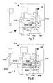
- FIG. 7 is a simplified illustration of still another embodiment of a precision apparatus 710 that is similar to the precision apparatus 10 described above. However, in this embodiment, the optical signals from the same optical fiber 728 are split with a fiber coupler 725 and are simultaneously directed at the spaced apart locations of the same optical filter 728 .
- the optical analyzer 714 includes (i) a first optical launcher 736 A that directs a first optical beam 718 A at the optical filter 728 , (ii) a first optical receiver 738 A that receives the first transmitted optical beam 724 A, (iii) a first beam detector 721 A that measures the magnitude of the first transmitted optical beam 724 A, (iv) a second optical launcher 736 B that directs a second optical beam 718 B at the optical filter 728 , (v) a second optical receiver 738 B that receives the second transmitted optical beam 724 B, and (vi) a second beam detector 721 B that measures the magnitude of the second transmitted optical beam 724 B.
- the optical signals are again split into two paths and applied to two parts of the optical filter 728 simultaneously. This can help deconvolve multiple input signals.
- FIG. 8 is a simplified illustration of yet another embodiment of a precision apparatus 810 that is similar to the precision apparatus 710 described above. However, in this embodiment, a first optical beam 818 A from a first optical fiber 816 A and a second optical beam 818 B from a second optical fiber 816 B are simultaneously directed at the spaced apart locations to the same optical filter 828 .
- the optical analyzer 814 includes (i) a first optical launcher 836 A that directs the first optical beam 818 A at the optical filter 828 , (ii) a first optical receiver 838 A that receives the first transmitted optical beam 824 A, (iii) a first beam detector 821 A that measures the magnitude of the first transmitted optical beam 824 A, (iv) a second optical launcher 836 B that directs the second optical beam 818 B at the optical filter 828 , (v) a second optical receiver 838 B that receives the second transmitted optical beam 824 B, and (vi) a second beam detector 821 B that measures the magnitude of the second transmitted optical beam 824 B.
- optical beams 818 A, 818 B can be analyzed simultaneously using many of the same components, without a significant increase in the number of parts. It should be noted that more than two optical beams 818 A, 818 B can be simultaneously directed at the optical filter 828 . With this design, the system is readily expandable.
- FIG. 9 is a simplified illustration of still another embodiment of a precision apparatus 910 that is similar to the precision apparatus 10 described above.
- the beam redirector 40 illustrated in FIG. 1
- the additional filter 976 could be made to transmit at 1523 nanometer, for example.
- the optical analyzer 914 would include a reference channel because the beam detector 921 would receive no signal when both the additional filter 976 and the center wavelength of the filter area 946 are aligned at 1520 nanometer. This eliminates the need for an additional wavelength reference.
- the additional filter 976 can be temperature insensitive etalon with the free spectral range (FSR) set such that there are two peaks in transmission. For example, one peak could be at 1523 nanometer and the other peak could be at 1577 nanometer. This gives a reference at both ends.
- FSR free spectral range
- the optical beams can be directed at near normal incidence to the optical filter.
- FIG. 10 is a plan view of another embodiment of an optical filter 1028 that is somewhat similar to the optical filter 28 described above.
- the filter area 1046 includes a full transmittance region 1078 that allows for the transmission of all wavelengths or a certain range of wavelengths, and a full block region 1080 that blocks all wavelengths or blocks a certain range of wavelengths.
- the full transmittance region 1078 and the full block region 1080 can be used during calibration of the optical analyzer 14 (illustrated in FIG. 1 ).
- FIG. 11 is a plan view of yet another embodiment of an optical filter 1128 that is somewhat similar to the optical filter 28 described above.
- the optical filter 1128 includes a first filter area 1146 A and a second filter area 1146 B.
- the filter areas 1146 A, 1146 B are concentric and each is shaped similar to an annular disk.
- the first filter area 1146 A can have a center wavelength that varies over a first center wavelength range and the second filter area 1146 B can have a center wavelength that varies over a second center wavelength range that is different than the first center wavelength range.
- the first optical launcher (not shown in FIG. 11 ) can direct the first optical beam (not shown in FIG.
- the same optical filter 1128 can be used to test multiple optical beams with different wavelengths.
- the first center wavelength range is approximately 1526 to 1575 nanometers to test the C band
- the second center wavelength range is approximately 1571 to 1610 nanometers to test the L band.
- the respective optical beam (not shown in FIGS. 10 and 11 ) can be directed at the respective filter areas at near normal incidence.
- FIG. 12 is a simplified illustration of yet another embodiment of a precision apparatus 1210 that is similar to the precision apparatus 10 described above.
- the optical filter 1228 is generally linear and the mover 1230 is a linear mover that moves the optical filter 1228 back and forth linearly.
- the position sensor 1232 monitors the linear position and movement rate of the optical filter 1228 .
- FIG. 13 is a graph that illustrates the alternative center wavelengths of one embodiment of an optical filter having features of the present invention. It should be noted that only a few of the center wavelengths of the optical filter are illustrated in FIG. 13 . Additionally, FIG. 13 illustrates that (i) the optical filter includes multiple different center wavelengths, (ii) the optical filter includes a plurality of relatively steep spherical slopes, and (iii) the optical filter is a narrow band pass filter having a relatively narrow bandwidth. It should be noted that other optical filter designs can be utilized.
Landscapes
- Physics & Mathematics (AREA)
- Spectroscopy & Molecular Physics (AREA)
- General Physics & Mathematics (AREA)
- Investigating Or Analysing Materials By Optical Means (AREA)
Abstract
Description
Claims (39)
Priority Applications (1)
| Application Number | Priority Date | Filing Date | Title |
|---|---|---|---|
| US11/716,238 US7826055B2 (en) | 2006-03-09 | 2007-03-09 | Optical channel analyzer with variable filter |
Applications Claiming Priority (2)
| Application Number | Priority Date | Filing Date | Title |
|---|---|---|---|
| US78094006P | 2006-03-09 | 2006-03-09 | |
| US11/716,238 US7826055B2 (en) | 2006-03-09 | 2007-03-09 | Optical channel analyzer with variable filter |
Publications (2)
| Publication Number | Publication Date |
|---|---|
| US20070222994A1 US20070222994A1 (en) | 2007-09-27 |
| US7826055B2 true US7826055B2 (en) | 2010-11-02 |
Family
ID=38533026
Family Applications (1)
| Application Number | Title | Priority Date | Filing Date |
|---|---|---|---|
| US11/716,238 Expired - Fee Related US7826055B2 (en) | 2006-03-09 | 2007-03-09 | Optical channel analyzer with variable filter |
Country Status (1)
| Country | Link |
|---|---|
| US (1) | US7826055B2 (en) |
Cited By (2)
| Publication number | Priority date | Publication date | Assignee | Title |
|---|---|---|---|---|
| US9645291B1 (en) | 2016-04-18 | 2017-05-09 | Ii-Vi Incorporated | Voltage-tunable optical filters for instrumentation applications |
| US11606147B1 (en) * | 2022-06-06 | 2023-03-14 | Bae Systems Information And Electronic Systems Integration Inc. | Frequency and bandwidth agile optical bench |
Citations (19)
| Publication number | Priority date | Publication date | Assignee | Title |
|---|---|---|---|---|
| US4957370A (en) * | 1984-06-21 | 1990-09-18 | Kabushiki Kaisha Toshiba | Method and apparatus for determining the degree of oxidation of an oxide coating |
| US5386295A (en) * | 1990-10-01 | 1995-01-31 | Eastman Kodak Company | Postacquired spectrophotometers |
| US6049411A (en) | 1998-10-14 | 2000-04-11 | Santec Systems Inc | Optical imager for birefringent detector acoustic imaging systems |
| US6094446A (en) | 1997-01-21 | 2000-07-25 | Santec Corporation | Wavelength stabilizing apparatus of laser light source |
| US6122301A (en) | 1998-06-17 | 2000-09-19 | Santec Corporation | Laser light source apparatus |
| US6144025A (en) | 1999-01-13 | 2000-11-07 | Santec Corporation | Laser light source apparatus |
| US6292616B1 (en) | 1998-08-04 | 2001-09-18 | Santec Corporation | Optical attenuator and optical attenuator module |
| US6371662B1 (en) * | 1997-11-26 | 2002-04-16 | Corning Lasertron, Inc. | Spatially variable filter laser wavelength monitoring/control |
| US20020171834A1 (en) * | 2001-04-11 | 2002-11-21 | Rowe Robert K. | Encoded variable filter spectrometer |
| US6765189B1 (en) | 2002-11-20 | 2004-07-20 | Santec U.S.A. Corporation | Small form factor in-line switched multichannel fiber optic power monitoring apparatus |
| US6816643B2 (en) | 2001-10-10 | 2004-11-09 | Santec Corporation | Wavelength tunable demultiplexing filter device, wavelength tunable multiplexing filter device, and wavelength routing device |
| US20050201432A1 (en) | 2004-03-10 | 2005-09-15 | Santec Corporation | Wide bandwidth light source |
| US20050219543A1 (en) | 2004-03-31 | 2005-10-06 | Santec Corporation | Optical pulse evaluation device and in-service optical pulse evaluation device |
| US20050261592A1 (en) * | 2004-05-21 | 2005-11-24 | Takeshi Suga | Fluorescence endoscope apparatus |
| US7006765B2 (en) | 1998-06-23 | 2006-02-28 | Jds Uniphase Corporation | Optical network monitor |
| US7099358B1 (en) | 2005-08-05 | 2006-08-29 | Santec Corporation | Tunable laser light source |
| US7120361B2 (en) | 2001-10-10 | 2006-10-10 | Santec Corporation | Wavelength tunable multiplexing and demultiplexing filter device and wavelength routing device |
| US7199927B2 (en) | 2003-06-10 | 2007-04-03 | Santec Corporation | Optical element and optical add-drop module |
| US7199928B2 (en) | 2003-07-17 | 2007-04-03 | Santec Corporation | Optical element, optical drop module, optical add-drop module, and tunable light source |
Family Cites Families (1)
| Publication number | Priority date | Publication date | Assignee | Title |
|---|---|---|---|---|
| EP1495622B1 (en) * | 2002-04-12 | 2009-03-25 | Thomson Licensing | Method for the anonymous authentication of a data transmitter |
-
2007
- 2007-03-09 US US11/716,238 patent/US7826055B2/en not_active Expired - Fee Related
Patent Citations (21)
| Publication number | Priority date | Publication date | Assignee | Title |
|---|---|---|---|---|
| US4957370A (en) * | 1984-06-21 | 1990-09-18 | Kabushiki Kaisha Toshiba | Method and apparatus for determining the degree of oxidation of an oxide coating |
| US5386295A (en) * | 1990-10-01 | 1995-01-31 | Eastman Kodak Company | Postacquired spectrophotometers |
| US6094446A (en) | 1997-01-21 | 2000-07-25 | Santec Corporation | Wavelength stabilizing apparatus of laser light source |
| US6371662B1 (en) * | 1997-11-26 | 2002-04-16 | Corning Lasertron, Inc. | Spatially variable filter laser wavelength monitoring/control |
| US6122301A (en) | 1998-06-17 | 2000-09-19 | Santec Corporation | Laser light source apparatus |
| US7006765B2 (en) | 1998-06-23 | 2006-02-28 | Jds Uniphase Corporation | Optical network monitor |
| US6292616B1 (en) | 1998-08-04 | 2001-09-18 | Santec Corporation | Optical attenuator and optical attenuator module |
| US20020001447A1 (en) | 1998-08-04 | 2002-01-03 | Santec Corporation | Optical attenuator and optical attenuator module |
| US6442324B2 (en) | 1998-08-04 | 2002-08-27 | Santec Corporation | Optical attenuator and optical attenuator module |
| US6049411A (en) | 1998-10-14 | 2000-04-11 | Santec Systems Inc | Optical imager for birefringent detector acoustic imaging systems |
| US6144025A (en) | 1999-01-13 | 2000-11-07 | Santec Corporation | Laser light source apparatus |
| US20020171834A1 (en) * | 2001-04-11 | 2002-11-21 | Rowe Robert K. | Encoded variable filter spectrometer |
| US6816643B2 (en) | 2001-10-10 | 2004-11-09 | Santec Corporation | Wavelength tunable demultiplexing filter device, wavelength tunable multiplexing filter device, and wavelength routing device |
| US7120361B2 (en) | 2001-10-10 | 2006-10-10 | Santec Corporation | Wavelength tunable multiplexing and demultiplexing filter device and wavelength routing device |
| US6765189B1 (en) | 2002-11-20 | 2004-07-20 | Santec U.S.A. Corporation | Small form factor in-line switched multichannel fiber optic power monitoring apparatus |
| US7199927B2 (en) | 2003-06-10 | 2007-04-03 | Santec Corporation | Optical element and optical add-drop module |
| US7199928B2 (en) | 2003-07-17 | 2007-04-03 | Santec Corporation | Optical element, optical drop module, optical add-drop module, and tunable light source |
| US20050201432A1 (en) | 2004-03-10 | 2005-09-15 | Santec Corporation | Wide bandwidth light source |
| US20050219543A1 (en) | 2004-03-31 | 2005-10-06 | Santec Corporation | Optical pulse evaluation device and in-service optical pulse evaluation device |
| US20050261592A1 (en) * | 2004-05-21 | 2005-11-24 | Takeshi Suga | Fluorescence endoscope apparatus |
| US7099358B1 (en) | 2005-08-05 | 2006-08-29 | Santec Corporation | Tunable laser light source |
Cited By (2)
| Publication number | Priority date | Publication date | Assignee | Title |
|---|---|---|---|---|
| US9645291B1 (en) | 2016-04-18 | 2017-05-09 | Ii-Vi Incorporated | Voltage-tunable optical filters for instrumentation applications |
| US11606147B1 (en) * | 2022-06-06 | 2023-03-14 | Bae Systems Information And Electronic Systems Integration Inc. | Frequency and bandwidth agile optical bench |
Also Published As
| Publication number | Publication date |
|---|---|
| US20070222994A1 (en) | 2007-09-27 |
Similar Documents
| Publication | Publication Date | Title |
|---|---|---|
| US6700690B1 (en) | Tunable variable bandpass optical filter | |
| US5357340A (en) | Method for spectroscopy using two Fabry-Perot interference filters | |
| US6344910B1 (en) | Optical performance monitor | |
| US5515169A (en) | Spectral wavelength discrimination system and method for using | |
| US6937346B2 (en) | Wavemeter having two interference elements | |
| US6646753B2 (en) | In-situ thickness and refractive index monitoring and control system for thin film deposition | |
| WO1989005465A1 (en) | Wedge-filter spectrometer | |
| WO2017016141A1 (en) | Performance testing device for multi-channel tunable laser | |
| US5850292A (en) | Wavelength monitor for optical signals | |
| FR2632404A1 (en) | INTERFEROMETRIC SENSOR AND ITS USE IN AN INTERFEROMETRIC DEVICE | |
| WO1982000717A1 (en) | Method and apparatus for photometric detection in fluids | |
| US7826055B2 (en) | Optical channel analyzer with variable filter | |
| CN109374130A (en) | A kind of band-pass adjustable optical filter and filtering method | |
| US20060055932A1 (en) | Self-referencing instrument and method thereof for measuring electromagnetic properties | |
| US4538910A (en) | Dual beam fourier spectrometer | |
| US6879744B2 (en) | Optical monitoring of thin film deposition | |
| US5321970A (en) | Method and apparatus for calibrating a spectrometer | |
| US7041959B1 (en) | System and method for monitoring the performance of dense wavelength division multiplexing optical communications systems | |
| JP2018511051A (en) | Measurement system and method for matching a birefringent optical sensor using a frequency swept source based interrogator | |
| US10267727B2 (en) | Determining polarization rotation characteristics of a sample taking into consideration a transmission dispersion | |
| US11313722B2 (en) | Infrared spectrometer having dielectric-polymer-based spectral filter | |
| US20030067601A1 (en) | Tunable filter with wavelength monitor | |
| CN205037969U (en) | Programme -controlled reputation spectral detection system gains based on variable OSK radio frequency modulation | |
| JP2006023330A (en) | Optical filter having a plurality of optical characteristics and application thereof to meteorological observation | |
| JP2003337080A (en) | Automatic measuring device for optical filter |
Legal Events
| Date | Code | Title | Description |
|---|---|---|---|
| AS | Assignment |
Owner name: BOOKHAM TECHNOLOGY PLC, UNITED KINGDOM Free format text: ASSIGNMENT OF ASSIGNORS INTEREST;ASSIGNORS:SCOBEY, MIKE;KEYS, ROBERT;SOMMER, RAD;SIGNING DATES FROM 20070531 TO 20070620;REEL/FRAME:019509/0366 Owner name: BOOKHAM TECHNOLOGY PLC, UNITED KINGDOM Free format text: ASSIGNMENT OF ASSIGNORS INTEREST;ASSIGNORS:SCOBEY, MIKE;KEYS, ROBERT;SOMMER, RAD;REEL/FRAME:019509/0366;SIGNING DATES FROM 20070531 TO 20070620 |
|
| AS | Assignment |
Owner name: WELLS FARGO FOOTHILL, INC., CALIFORNIA Free format text: AMENDMENT TO PATENT SECURITY AGREEMENT;ASSIGNOR:OCLARO TECHNOLOGY PLC;REEL/FRAME:023260/0955 Effective date: 20090810 Owner name: WELLS FARGO FOOTHILL, INC.,CALIFORNIA Free format text: AMENDMENT TO PATENT SECURITY AGREEMENT;ASSIGNOR:OCLARO TECHNOLOGY PLC;REEL/FRAME:023260/0955 Effective date: 20090810 |
|
| AS | Assignment |
Owner name: OCLARO TECHNOLOGY PLC, UNITED KINGDOM Free format text: CHANGE OF NAME;ASSIGNOR:BOOKHAM TECHNOLOGY PLC;REEL/FRAME:025033/0795 Effective date: 20070625 |
|
| AS | Assignment |
Owner name: OCLARO TECHNOLOGY LIMITED, UNITED KINGDOM Free format text: CHANGE OF NAME;ASSIGNOR:OCLARO TECHNOLOGY PLC;REEL/FRAME:025045/0019 Effective date: 20100630 |
|
| AS | Assignment |
Owner name: II-VI INCORPORATED, PENNSYLVANIA Free format text: ASSIGNMENT OF ASSIGNORS INTEREST;ASSIGNORS:OCLARO TECHNOLOGY LIMITED;OCLARO, INC.;OCLARO (NORTH AMERICA), INC.;AND OTHERS;REEL/FRAME:032554/0818 Effective date: 20131101 |
|
| AS | Assignment |
Owner name: OCLARO, INC., CALIFORNIA Free format text: RELEASE OF SECURITY INTEREST;ASSIGNOR:WELLS FARGO CAPITAL FINANCE, LLC;REEL/FRAME:032982/0222 Effective date: 20131101 Owner name: OCLARO TECHNOLOGY LIMITED, CALIFORNIA Free format text: RELEASE OF SECURITY INTEREST;ASSIGNOR:WELLS FARGO CAPITAL FINANCE, LLC;REEL/FRAME:032982/0222 Effective date: 20131101 |
|
| REMI | Maintenance fee reminder mailed | ||
| LAPS | Lapse for failure to pay maintenance fees | ||
| STCH | Information on status: patent discontinuation |
Free format text: PATENT EXPIRED DUE TO NONPAYMENT OF MAINTENANCE FEES UNDER 37 CFR 1.362 |
|
| FP | Expired due to failure to pay maintenance fee |
Effective date: 20141102 |