US7821120B2 - Metal filled through via structure for providing vertical wafer-to-wafer interconnection - Google Patents
Metal filled through via structure for providing vertical wafer-to-wafer interconnection Download PDFInfo
- Publication number
- US7821120B2 US7821120B2 US11/971,581 US97158108A US7821120B2 US 7821120 B2 US7821120 B2 US 7821120B2 US 97158108 A US97158108 A US 97158108A US 7821120 B2 US7821120 B2 US 7821120B2
- Authority
- US
- United States
- Prior art keywords
- wafer
- metal
- interconnect structure
- vertical
- recited
- Prior art date
- Legal status (The legal status is an assumption and is not a legal conclusion. Google has not performed a legal analysis and makes no representation as to the accuracy of the status listed.)
- Active, expires
Links
- 239000002184 metal Substances 0.000 title claims abstract description 112
- 229910052751 metal Inorganic materials 0.000 title claims abstract description 112
- 235000012431 wafers Nutrition 0.000 claims abstract description 153
- 239000004642 Polyimide Substances 0.000 claims abstract description 57
- 229920001721 polyimide Polymers 0.000 claims abstract description 57
- 239000011248 coating agent Substances 0.000 claims abstract description 34
- 238000000576 coating method Methods 0.000 claims abstract description 34
- 230000005855 radiation Effects 0.000 claims abstract description 18
- 239000004065 semiconductor Substances 0.000 claims description 70
- 239000000758 substrate Substances 0.000 claims description 40
- 239000003989 dielectric material Substances 0.000 claims description 34
- 239000000463 material Substances 0.000 claims description 13
- 229910052802 copper Inorganic materials 0.000 claims description 4
- 229910052782 aluminium Inorganic materials 0.000 claims description 3
- 229910052721 tungsten Inorganic materials 0.000 claims description 3
- 229910052737 gold Inorganic materials 0.000 claims description 2
- 238000000034 method Methods 0.000 description 32
- 238000012545 processing Methods 0.000 description 18
- 239000010949 copper Substances 0.000 description 16
- 239000010410 layer Substances 0.000 description 14
- 238000010438 heat treatment Methods 0.000 description 11
- 238000005530 etching Methods 0.000 description 8
- 238000005275 alloying Methods 0.000 description 7
- 239000013078 crystal Substances 0.000 description 5
- 238000003780 insertion Methods 0.000 description 5
- 230000037431 insertion Effects 0.000 description 5
- 238000001459 lithography Methods 0.000 description 5
- 229920002120 photoresistant polymer Polymers 0.000 description 5
- VYPSYNLAJGMNEJ-UHFFFAOYSA-N Silicium dioxide Chemical compound O=[Si]=O VYPSYNLAJGMNEJ-UHFFFAOYSA-N 0.000 description 4
- 238000013459 approach Methods 0.000 description 4
- 238000005229 chemical vapour deposition Methods 0.000 description 4
- 238000000151 deposition Methods 0.000 description 4
- 238000005137 deposition process Methods 0.000 description 4
- 238000004519 manufacturing process Methods 0.000 description 4
- 238000000623 plasma-assisted chemical vapour deposition Methods 0.000 description 4
- 125000006850 spacer group Chemical group 0.000 description 4
- 230000015572 biosynthetic process Effects 0.000 description 3
- 238000001704 evaporation Methods 0.000 description 3
- 230000008020 evaporation Effects 0.000 description 3
- 150000002739 metals Chemical class 0.000 description 3
- 229920006259 thermoplastic polyimide Polymers 0.000 description 3
- 238000012546 transfer Methods 0.000 description 3
- 229910000577 Silicon-germanium Inorganic materials 0.000 description 2
- 238000000231 atomic layer deposition Methods 0.000 description 2
- 230000034303 cell budding Effects 0.000 description 2
- 229910052681 coesite Inorganic materials 0.000 description 2
- 229910052906 cristobalite Inorganic materials 0.000 description 2
- 230000008021 deposition Effects 0.000 description 2
- 238000011049 filling Methods 0.000 description 2
- 238000000227 grinding Methods 0.000 description 2
- 239000012212 insulator Substances 0.000 description 2
- 238000005468 ion implantation Methods 0.000 description 2
- 238000005304 joining Methods 0.000 description 2
- 239000000203 mixture Substances 0.000 description 2
- 150000004767 nitrides Chemical class 0.000 description 2
- 238000001020 plasma etching Methods 0.000 description 2
- 229910052710 silicon Inorganic materials 0.000 description 2
- 239000000377 silicon dioxide Substances 0.000 description 2
- 229910000679 solder Inorganic materials 0.000 description 2
- 229910052682 stishovite Inorganic materials 0.000 description 2
- 229910052905 tridymite Inorganic materials 0.000 description 2
- 229910016570 AlCu Inorganic materials 0.000 description 1
- RYGMFSIKBFXOCR-UHFFFAOYSA-N Copper Chemical compound [Cu] RYGMFSIKBFXOCR-UHFFFAOYSA-N 0.000 description 1
- 229910001218 Gallium arsenide Inorganic materials 0.000 description 1
- 229910000673 Indium arsenide Inorganic materials 0.000 description 1
- 229910003811 SiGeC Inorganic materials 0.000 description 1
- ATJFFYVFTNAWJD-UHFFFAOYSA-N Tin Chemical compound [Sn] ATJFFYVFTNAWJD-UHFFFAOYSA-N 0.000 description 1
- 239000000853 adhesive Substances 0.000 description 1
- 230000001070 adhesive effect Effects 0.000 description 1
- 238000000137 annealing Methods 0.000 description 1
- QVGXLLKOCUKJST-UHFFFAOYSA-N atomic oxygen Chemical compound [O] QVGXLLKOCUKJST-UHFFFAOYSA-N 0.000 description 1
- 239000007767 bonding agent Substances 0.000 description 1
- 239000000919 ceramic Substances 0.000 description 1
- 238000000224 chemical solution deposition Methods 0.000 description 1
- 150000001875 compounds Chemical class 0.000 description 1
- 230000001419 dependent effect Effects 0.000 description 1
- 238000001312 dry etching Methods 0.000 description 1
- 238000009713 electroplating Methods 0.000 description 1
- 230000008030 elimination Effects 0.000 description 1
- 238000003379 elimination reaction Methods 0.000 description 1
- 230000005669 field effect Effects 0.000 description 1
- 229910052732 germanium Inorganic materials 0.000 description 1
- RPQDHPTXJYYUPQ-UHFFFAOYSA-N indium arsenide Chemical compound [In]#[As] RPQDHPTXJYYUPQ-UHFFFAOYSA-N 0.000 description 1
- 238000010884 ion-beam technique Methods 0.000 description 1
- 238000000608 laser ablation Methods 0.000 description 1
- 229910003465 moissanite Inorganic materials 0.000 description 1
- 230000003647 oxidation Effects 0.000 description 1
- 238000007254 oxidation reaction Methods 0.000 description 1
- 229910052760 oxygen Inorganic materials 0.000 description 1
- 239000001301 oxygen Substances 0.000 description 1
- 238000004806 packaging method and process Methods 0.000 description 1
- 238000005498 polishing Methods 0.000 description 1
- 230000001681 protective effect Effects 0.000 description 1
- 239000011241 protective layer Substances 0.000 description 1
- 238000000926 separation method Methods 0.000 description 1
- 239000010703 silicon Substances 0.000 description 1
- 229910010271 silicon carbide Inorganic materials 0.000 description 1
- 239000000126 substance Substances 0.000 description 1
- 238000003631 wet chemical etching Methods 0.000 description 1
- 238000001039 wet etching Methods 0.000 description 1
Images


Classifications
-
- H—ELECTRICITY
- H01—ELECTRIC ELEMENTS
- H01L—SEMICONDUCTOR DEVICES NOT COVERED BY CLASS H10
- H01L23/00—Details of semiconductor or other solid state devices
- H01L23/52—Arrangements for conducting electric current within the device in operation from one component to another, i.e. interconnections, e.g. wires, lead frames
-
- H—ELECTRICITY
- H01—ELECTRIC ELEMENTS
- H01L—SEMICONDUCTOR DEVICES NOT COVERED BY CLASS H10
- H01L24/00—Arrangements for connecting or disconnecting semiconductor or solid-state bodies; Methods or apparatus related thereto
- H01L24/90—Methods for connecting semiconductor or solid state bodies using means for bonding not being attached to, or not being formed on, the body surface to be connected, e.g. pressure contacts using springs or clips
-
- H—ELECTRICITY
- H01—ELECTRIC ELEMENTS
- H01L—SEMICONDUCTOR DEVICES NOT COVERED BY CLASS H10
- H01L21/00—Processes or apparatus adapted for the manufacture or treatment of semiconductor or solid state devices or of parts thereof
- H01L21/70—Manufacture or treatment of devices consisting of a plurality of solid state components formed in or on a common substrate or of parts thereof; Manufacture of integrated circuit devices or of parts thereof
- H01L21/71—Manufacture of specific parts of devices defined in group H01L21/70
- H01L21/768—Applying interconnections to be used for carrying current between separate components within a device comprising conductors and dielectrics
- H01L21/76898—Applying interconnections to be used for carrying current between separate components within a device comprising conductors and dielectrics formed through a semiconductor substrate
-
- H—ELECTRICITY
- H01—ELECTRIC ELEMENTS
- H01L—SEMICONDUCTOR DEVICES NOT COVERED BY CLASS H10
- H01L24/00—Arrangements for connecting or disconnecting semiconductor or solid-state bodies; Methods or apparatus related thereto
- H01L24/01—Means for bonding being attached to, or being formed on, the surface to be connected, e.g. chip-to-package, die-attach, "first-level" interconnects; Manufacturing methods related thereto
- H01L24/02—Bonding areas ; Manufacturing methods related thereto
- H01L24/03—Manufacturing methods
-
- H—ELECTRICITY
- H01—ELECTRIC ELEMENTS
- H01L—SEMICONDUCTOR DEVICES NOT COVERED BY CLASS H10
- H01L24/00—Arrangements for connecting or disconnecting semiconductor or solid-state bodies; Methods or apparatus related thereto
- H01L24/01—Means for bonding being attached to, or being formed on, the surface to be connected, e.g. chip-to-package, die-attach, "first-level" interconnects; Manufacturing methods related thereto
- H01L24/02—Bonding areas ; Manufacturing methods related thereto
- H01L24/04—Structure, shape, material or disposition of the bonding areas prior to the connecting process
- H01L24/05—Structure, shape, material or disposition of the bonding areas prior to the connecting process of an individual bonding area
-
- H—ELECTRICITY
- H01—ELECTRIC ELEMENTS
- H01L—SEMICONDUCTOR DEVICES NOT COVERED BY CLASS H10
- H01L24/00—Arrangements for connecting or disconnecting semiconductor or solid-state bodies; Methods or apparatus related thereto
- H01L24/01—Means for bonding being attached to, or being formed on, the surface to be connected, e.g. chip-to-package, die-attach, "first-level" interconnects; Manufacturing methods related thereto
- H01L24/10—Bump connectors ; Manufacturing methods related thereto
- H01L24/12—Structure, shape, material or disposition of the bump connectors prior to the connecting process
- H01L24/13—Structure, shape, material or disposition of the bump connectors prior to the connecting process of an individual bump connector
-
- H—ELECTRICITY
- H01—ELECTRIC ELEMENTS
- H01L—SEMICONDUCTOR DEVICES NOT COVERED BY CLASS H10
- H01L24/00—Arrangements for connecting or disconnecting semiconductor or solid-state bodies; Methods or apparatus related thereto
- H01L24/01—Means for bonding being attached to, or being formed on, the surface to be connected, e.g. chip-to-package, die-attach, "first-level" interconnects; Manufacturing methods related thereto
- H01L24/10—Bump connectors ; Manufacturing methods related thereto
- H01L24/15—Structure, shape, material or disposition of the bump connectors after the connecting process
- H01L24/16—Structure, shape, material or disposition of the bump connectors after the connecting process of an individual bump connector
-
- H—ELECTRICITY
- H01—ELECTRIC ELEMENTS
- H01L—SEMICONDUCTOR DEVICES NOT COVERED BY CLASS H10
- H01L24/00—Arrangements for connecting or disconnecting semiconductor or solid-state bodies; Methods or apparatus related thereto
- H01L24/01—Means for bonding being attached to, or being formed on, the surface to be connected, e.g. chip-to-package, die-attach, "first-level" interconnects; Manufacturing methods related thereto
- H01L24/26—Layer connectors, e.g. plate connectors, solder or adhesive layers; Manufacturing methods related thereto
- H01L24/28—Structure, shape, material or disposition of the layer connectors prior to the connecting process
-
- H—ELECTRICITY
- H01—ELECTRIC ELEMENTS
- H01L—SEMICONDUCTOR DEVICES NOT COVERED BY CLASS H10
- H01L24/00—Arrangements for connecting or disconnecting semiconductor or solid-state bodies; Methods or apparatus related thereto
- H01L24/80—Methods for connecting semiconductor or other solid state bodies using means for bonding being attached to, or being formed on, the surface to be connected
- H01L24/83—Methods for connecting semiconductor or other solid state bodies using means for bonding being attached to, or being formed on, the surface to be connected using a layer connector
-
- H—ELECTRICITY
- H01—ELECTRIC ELEMENTS
- H01L—SEMICONDUCTOR DEVICES NOT COVERED BY CLASS H10
- H01L24/00—Arrangements for connecting or disconnecting semiconductor or solid-state bodies; Methods or apparatus related thereto
- H01L24/93—Batch processes
- H01L24/94—Batch processes at wafer-level, i.e. with connecting carried out on a wafer comprising a plurality of undiced individual devices
-
- H—ELECTRICITY
- H01—ELECTRIC ELEMENTS
- H01L—SEMICONDUCTOR DEVICES NOT COVERED BY CLASS H10
- H01L25/00—Assemblies consisting of a plurality of semiconductor or other solid state devices
- H01L25/03—Assemblies consisting of a plurality of semiconductor or other solid state devices all the devices being of a type provided for in a single subclass of subclasses H10B, H10F, H10H, H10K or H10N, e.g. assemblies of rectifier diodes
- H01L25/04—Assemblies consisting of a plurality of semiconductor or other solid state devices all the devices being of a type provided for in a single subclass of subclasses H10B, H10F, H10H, H10K or H10N, e.g. assemblies of rectifier diodes the devices not having separate containers
- H01L25/065—Assemblies consisting of a plurality of semiconductor or other solid state devices all the devices being of a type provided for in a single subclass of subclasses H10B, H10F, H10H, H10K or H10N, e.g. assemblies of rectifier diodes the devices not having separate containers the devices being of a type provided for in group H10D89/00
- H01L25/0657—Stacked arrangements of devices
-
- H—ELECTRICITY
- H01—ELECTRIC ELEMENTS
- H01L—SEMICONDUCTOR DEVICES NOT COVERED BY CLASS H10
- H01L25/00—Assemblies consisting of a plurality of semiconductor or other solid state devices
- H01L25/50—Multistep manufacturing processes of assemblies consisting of devices, the devices being individual devices of subclass H10D or integrated devices of class H10
-
- H—ELECTRICITY
- H01—ELECTRIC ELEMENTS
- H01L—SEMICONDUCTOR DEVICES NOT COVERED BY CLASS H10
- H01L2224/00—Indexing scheme for arrangements for connecting or disconnecting semiconductor or solid-state bodies and methods related thereto as covered by H01L24/00
- H01L2224/01—Means for bonding being attached to, or being formed on, the surface to be connected, e.g. chip-to-package, die-attach, "first-level" interconnects; Manufacturing methods related thereto
- H01L2224/02—Bonding areas; Manufacturing methods related thereto
- H01L2224/04—Structure, shape, material or disposition of the bonding areas prior to the connecting process
- H01L2224/0401—Bonding areas specifically adapted for bump connectors, e.g. under bump metallisation [UBM]
-
- H—ELECTRICITY
- H01—ELECTRIC ELEMENTS
- H01L—SEMICONDUCTOR DEVICES NOT COVERED BY CLASS H10
- H01L2224/00—Indexing scheme for arrangements for connecting or disconnecting semiconductor or solid-state bodies and methods related thereto as covered by H01L24/00
- H01L2224/01—Means for bonding being attached to, or being formed on, the surface to be connected, e.g. chip-to-package, die-attach, "first-level" interconnects; Manufacturing methods related thereto
- H01L2224/02—Bonding areas; Manufacturing methods related thereto
- H01L2224/04—Structure, shape, material or disposition of the bonding areas prior to the connecting process
- H01L2224/05—Structure, shape, material or disposition of the bonding areas prior to the connecting process of an individual bonding area
- H01L2224/0554—External layer
- H01L2224/0556—Disposition
- H01L2224/0557—Disposition the external layer being disposed on a via connection of the semiconductor or solid-state body
-
- H—ELECTRICITY
- H01—ELECTRIC ELEMENTS
- H01L—SEMICONDUCTOR DEVICES NOT COVERED BY CLASS H10
- H01L2224/00—Indexing scheme for arrangements for connecting or disconnecting semiconductor or solid-state bodies and methods related thereto as covered by H01L24/00
- H01L2224/01—Means for bonding being attached to, or being formed on, the surface to be connected, e.g. chip-to-package, die-attach, "first-level" interconnects; Manufacturing methods related thereto
- H01L2224/02—Bonding areas; Manufacturing methods related thereto
- H01L2224/04—Structure, shape, material or disposition of the bonding areas prior to the connecting process
- H01L2224/05—Structure, shape, material or disposition of the bonding areas prior to the connecting process of an individual bonding area
- H01L2224/0554—External layer
- H01L2224/05599—Material
- H01L2224/056—Material with a principal constituent of the material being a metal or a metalloid, e.g. boron [B], silicon [Si], germanium [Ge], arsenic [As], antimony [Sb], tellurium [Te] and polonium [Po], and alloys thereof
- H01L2224/05638—Material with a principal constituent of the material being a metal or a metalloid, e.g. boron [B], silicon [Si], germanium [Ge], arsenic [As], antimony [Sb], tellurium [Te] and polonium [Po], and alloys thereof the principal constituent melting at a temperature of greater than or equal to 950°C and less than 1550°C
- H01L2224/05647—Copper [Cu] as principal constituent
-
- H—ELECTRICITY
- H01—ELECTRIC ELEMENTS
- H01L—SEMICONDUCTOR DEVICES NOT COVERED BY CLASS H10
- H01L2224/00—Indexing scheme for arrangements for connecting or disconnecting semiconductor or solid-state bodies and methods related thereto as covered by H01L24/00
- H01L2224/01—Means for bonding being attached to, or being formed on, the surface to be connected, e.g. chip-to-package, die-attach, "first-level" interconnects; Manufacturing methods related thereto
- H01L2224/10—Bump connectors; Manufacturing methods related thereto
- H01L2224/12—Structure, shape, material or disposition of the bump connectors prior to the connecting process
- H01L2224/13—Structure, shape, material or disposition of the bump connectors prior to the connecting process of an individual bump connector
- H01L2224/13001—Core members of the bump connector
- H01L2224/13005—Structure
- H01L2224/13009—Bump connector integrally formed with a via connection of the semiconductor or solid-state body
-
- H—ELECTRICITY
- H01—ELECTRIC ELEMENTS
- H01L—SEMICONDUCTOR DEVICES NOT COVERED BY CLASS H10
- H01L2224/00—Indexing scheme for arrangements for connecting or disconnecting semiconductor or solid-state bodies and methods related thereto as covered by H01L24/00
- H01L2224/01—Means for bonding being attached to, or being formed on, the surface to be connected, e.g. chip-to-package, die-attach, "first-level" interconnects; Manufacturing methods related thereto
- H01L2224/10—Bump connectors; Manufacturing methods related thereto
- H01L2224/12—Structure, shape, material or disposition of the bump connectors prior to the connecting process
- H01L2224/13—Structure, shape, material or disposition of the bump connectors prior to the connecting process of an individual bump connector
- H01L2224/13001—Core members of the bump connector
- H01L2224/13099—Material
- H01L2224/131—Material with a principal constituent of the material being a metal or a metalloid, e.g. boron [B], silicon [Si], germanium [Ge], arsenic [As], antimony [Sb], tellurium [Te] and polonium [Po], and alloys thereof
- H01L2224/13117—Material with a principal constituent of the material being a metal or a metalloid, e.g. boron [B], silicon [Si], germanium [Ge], arsenic [As], antimony [Sb], tellurium [Te] and polonium [Po], and alloys thereof the principal constituent melting at a temperature of greater than or equal to 400°C and less than 950°C
- H01L2224/13124—Aluminium [Al] as principal constituent
-
- H—ELECTRICITY
- H01—ELECTRIC ELEMENTS
- H01L—SEMICONDUCTOR DEVICES NOT COVERED BY CLASS H10
- H01L2224/00—Indexing scheme for arrangements for connecting or disconnecting semiconductor or solid-state bodies and methods related thereto as covered by H01L24/00
- H01L2224/01—Means for bonding being attached to, or being formed on, the surface to be connected, e.g. chip-to-package, die-attach, "first-level" interconnects; Manufacturing methods related thereto
- H01L2224/10—Bump connectors; Manufacturing methods related thereto
- H01L2224/12—Structure, shape, material or disposition of the bump connectors prior to the connecting process
- H01L2224/13—Structure, shape, material or disposition of the bump connectors prior to the connecting process of an individual bump connector
- H01L2224/13001—Core members of the bump connector
- H01L2224/13099—Material
- H01L2224/131—Material with a principal constituent of the material being a metal or a metalloid, e.g. boron [B], silicon [Si], germanium [Ge], arsenic [As], antimony [Sb], tellurium [Te] and polonium [Po], and alloys thereof
- H01L2224/13138—Material with a principal constituent of the material being a metal or a metalloid, e.g. boron [B], silicon [Si], germanium [Ge], arsenic [As], antimony [Sb], tellurium [Te] and polonium [Po], and alloys thereof the principal constituent melting at a temperature of greater than or equal to 950°C and less than 1550°C
- H01L2224/13144—Gold [Au] as principal constituent
-
- H—ELECTRICITY
- H01—ELECTRIC ELEMENTS
- H01L—SEMICONDUCTOR DEVICES NOT COVERED BY CLASS H10
- H01L2224/00—Indexing scheme for arrangements for connecting or disconnecting semiconductor or solid-state bodies and methods related thereto as covered by H01L24/00
- H01L2224/01—Means for bonding being attached to, or being formed on, the surface to be connected, e.g. chip-to-package, die-attach, "first-level" interconnects; Manufacturing methods related thereto
- H01L2224/10—Bump connectors; Manufacturing methods related thereto
- H01L2224/12—Structure, shape, material or disposition of the bump connectors prior to the connecting process
- H01L2224/13—Structure, shape, material or disposition of the bump connectors prior to the connecting process of an individual bump connector
- H01L2224/13001—Core members of the bump connector
- H01L2224/13099—Material
- H01L2224/131—Material with a principal constituent of the material being a metal or a metalloid, e.g. boron [B], silicon [Si], germanium [Ge], arsenic [As], antimony [Sb], tellurium [Te] and polonium [Po], and alloys thereof
- H01L2224/13138—Material with a principal constituent of the material being a metal or a metalloid, e.g. boron [B], silicon [Si], germanium [Ge], arsenic [As], antimony [Sb], tellurium [Te] and polonium [Po], and alloys thereof the principal constituent melting at a temperature of greater than or equal to 950°C and less than 1550°C
- H01L2224/13147—Copper [Cu] as principal constituent
-
- H—ELECTRICITY
- H01—ELECTRIC ELEMENTS
- H01L—SEMICONDUCTOR DEVICES NOT COVERED BY CLASS H10
- H01L2224/00—Indexing scheme for arrangements for connecting or disconnecting semiconductor or solid-state bodies and methods related thereto as covered by H01L24/00
- H01L2224/01—Means for bonding being attached to, or being formed on, the surface to be connected, e.g. chip-to-package, die-attach, "first-level" interconnects; Manufacturing methods related thereto
- H01L2224/10—Bump connectors; Manufacturing methods related thereto
- H01L2224/15—Structure, shape, material or disposition of the bump connectors after the connecting process
- H01L2224/16—Structure, shape, material or disposition of the bump connectors after the connecting process of an individual bump connector
- H01L2224/161—Disposition
- H01L2224/16135—Disposition the bump connector connecting between different semiconductor or solid-state bodies, i.e. chip-to-chip
- H01L2224/16145—Disposition the bump connector connecting between different semiconductor or solid-state bodies, i.e. chip-to-chip the bodies being stacked
- H01L2224/16147—Disposition the bump connector connecting between different semiconductor or solid-state bodies, i.e. chip-to-chip the bodies being stacked the bump connector connecting to a bonding area disposed in a recess of the surface
-
- H—ELECTRICITY
- H01—ELECTRIC ELEMENTS
- H01L—SEMICONDUCTOR DEVICES NOT COVERED BY CLASS H10
- H01L2224/00—Indexing scheme for arrangements for connecting or disconnecting semiconductor or solid-state bodies and methods related thereto as covered by H01L24/00
- H01L2224/01—Means for bonding being attached to, or being formed on, the surface to be connected, e.g. chip-to-package, die-attach, "first-level" interconnects; Manufacturing methods related thereto
- H01L2224/10—Bump connectors; Manufacturing methods related thereto
- H01L2224/15—Structure, shape, material or disposition of the bump connectors after the connecting process
- H01L2224/16—Structure, shape, material or disposition of the bump connectors after the connecting process of an individual bump connector
- H01L2224/161—Disposition
- H01L2224/16151—Disposition the bump connector connecting between a semiconductor or solid-state body and an item not being a semiconductor or solid-state body, e.g. chip-to-substrate, chip-to-passive
- H01L2224/16221—Disposition the bump connector connecting between a semiconductor or solid-state body and an item not being a semiconductor or solid-state body, e.g. chip-to-substrate, chip-to-passive the body and the item being stacked
- H01L2224/16225—Disposition the bump connector connecting between a semiconductor or solid-state body and an item not being a semiconductor or solid-state body, e.g. chip-to-substrate, chip-to-passive the body and the item being stacked the item being non-metallic, e.g. insulating substrate with or without metallisation
- H01L2224/16237—Disposition the bump connector connecting between a semiconductor or solid-state body and an item not being a semiconductor or solid-state body, e.g. chip-to-substrate, chip-to-passive the body and the item being stacked the item being non-metallic, e.g. insulating substrate with or without metallisation the bump connector connecting to a bonding area disposed in a recess of the surface of the item
-
- H—ELECTRICITY
- H01—ELECTRIC ELEMENTS
- H01L—SEMICONDUCTOR DEVICES NOT COVERED BY CLASS H10
- H01L2224/00—Indexing scheme for arrangements for connecting or disconnecting semiconductor or solid-state bodies and methods related thereto as covered by H01L24/00
- H01L2224/80—Methods for connecting semiconductor or other solid state bodies using means for bonding being attached to, or being formed on, the surface to be connected
- H01L2224/81—Methods for connecting semiconductor or other solid state bodies using means for bonding being attached to, or being formed on, the surface to be connected using a bump connector
- H01L2224/8112—Aligning
- H01L2224/81136—Aligning involving guiding structures, e.g. spacers or supporting members
- H01L2224/81138—Aligning involving guiding structures, e.g. spacers or supporting members the guiding structures being at least partially left in the finished device
- H01L2224/81141—Guiding structures both on and outside the body
-
- H—ELECTRICITY
- H01—ELECTRIC ELEMENTS
- H01L—SEMICONDUCTOR DEVICES NOT COVERED BY CLASS H10
- H01L2224/00—Indexing scheme for arrangements for connecting or disconnecting semiconductor or solid-state bodies and methods related thereto as covered by H01L24/00
- H01L2224/80—Methods for connecting semiconductor or other solid state bodies using means for bonding being attached to, or being formed on, the surface to be connected
- H01L2224/81—Methods for connecting semiconductor or other solid state bodies using means for bonding being attached to, or being formed on, the surface to be connected using a bump connector
- H01L2224/8119—Arrangement of the bump connectors prior to mounting
- H01L2224/81191—Arrangement of the bump connectors prior to mounting wherein the bump connectors are disposed only on the semiconductor or solid-state body
-
- H—ELECTRICITY
- H01—ELECTRIC ELEMENTS
- H01L—SEMICONDUCTOR DEVICES NOT COVERED BY CLASS H10
- H01L2224/00—Indexing scheme for arrangements for connecting or disconnecting semiconductor or solid-state bodies and methods related thereto as covered by H01L24/00
- H01L2224/80—Methods for connecting semiconductor or other solid state bodies using means for bonding being attached to, or being formed on, the surface to be connected
- H01L2224/83—Methods for connecting semiconductor or other solid state bodies using means for bonding being attached to, or being formed on, the surface to be connected using a layer connector
- H01L2224/8319—Arrangement of the layer connectors prior to mounting
- H01L2224/83194—Lateral distribution of the layer connectors
-
- H—ELECTRICITY
- H01—ELECTRIC ELEMENTS
- H01L—SEMICONDUCTOR DEVICES NOT COVERED BY CLASS H10
- H01L2224/00—Indexing scheme for arrangements for connecting or disconnecting semiconductor or solid-state bodies and methods related thereto as covered by H01L24/00
- H01L2224/80—Methods for connecting semiconductor or other solid state bodies using means for bonding being attached to, or being formed on, the surface to be connected
- H01L2224/83—Methods for connecting semiconductor or other solid state bodies using means for bonding being attached to, or being formed on, the surface to be connected using a layer connector
- H01L2224/838—Bonding techniques
-
- H—ELECTRICITY
- H01—ELECTRIC ELEMENTS
- H01L—SEMICONDUCTOR DEVICES NOT COVERED BY CLASS H10
- H01L2224/00—Indexing scheme for arrangements for connecting or disconnecting semiconductor or solid-state bodies and methods related thereto as covered by H01L24/00
- H01L2224/91—Methods for connecting semiconductor or solid state bodies including different methods provided for in two or more of groups H01L2224/80 - H01L2224/90
- H01L2224/92—Specific sequence of method steps
- H01L2224/9201—Forming connectors during the connecting process, e.g. in-situ formation of bumps
-
- H—ELECTRICITY
- H01—ELECTRIC ELEMENTS
- H01L—SEMICONDUCTOR DEVICES NOT COVERED BY CLASS H10
- H01L2224/00—Indexing scheme for arrangements for connecting or disconnecting semiconductor or solid-state bodies and methods related thereto as covered by H01L24/00
- H01L2224/91—Methods for connecting semiconductor or solid state bodies including different methods provided for in two or more of groups H01L2224/80 - H01L2224/90
- H01L2224/92—Specific sequence of method steps
- H01L2224/9202—Forming additional connectors after the connecting process
-
- H—ELECTRICITY
- H01—ELECTRIC ELEMENTS
- H01L—SEMICONDUCTOR DEVICES NOT COVERED BY CLASS H10
- H01L2225/00—Details relating to assemblies covered by the group H01L25/00 but not provided for in its subgroups
- H01L2225/03—All the devices being of a type provided for in the same main group of the same subclass of class H10, e.g. assemblies of rectifier diodes
- H01L2225/04—All the devices being of a type provided for in the same main group of the same subclass of class H10, e.g. assemblies of rectifier diodes the devices not having separate containers
- H01L2225/065—All the devices being of a type provided for in the same main group of the same subclass of class H10
- H01L2225/06503—Stacked arrangements of devices
- H01L2225/06513—Bump or bump-like direct electrical connections between devices, e.g. flip-chip connection, solder bumps
-
- H—ELECTRICITY
- H01—ELECTRIC ELEMENTS
- H01L—SEMICONDUCTOR DEVICES NOT COVERED BY CLASS H10
- H01L2225/00—Details relating to assemblies covered by the group H01L25/00 but not provided for in its subgroups
- H01L2225/03—All the devices being of a type provided for in the same main group of the same subclass of class H10, e.g. assemblies of rectifier diodes
- H01L2225/04—All the devices being of a type provided for in the same main group of the same subclass of class H10, e.g. assemblies of rectifier diodes the devices not having separate containers
- H01L2225/065—All the devices being of a type provided for in the same main group of the same subclass of class H10
- H01L2225/06503—Stacked arrangements of devices
- H01L2225/06541—Conductive via connections through the device, e.g. vertical interconnects, through silicon via [TSV]
-
- H—ELECTRICITY
- H01—ELECTRIC ELEMENTS
- H01L—SEMICONDUCTOR DEVICES NOT COVERED BY CLASS H10
- H01L2924/00—Indexing scheme for arrangements or methods for connecting or disconnecting semiconductor or solid-state bodies as covered by H01L24/00
- H01L2924/0001—Technical content checked by a classifier
- H01L2924/0002—Not covered by any one of groups H01L24/00, H01L24/00 and H01L2224/00
-
- H—ELECTRICITY
- H01—ELECTRIC ELEMENTS
- H01L—SEMICONDUCTOR DEVICES NOT COVERED BY CLASS H10
- H01L2924/00—Indexing scheme for arrangements or methods for connecting or disconnecting semiconductor or solid-state bodies as covered by H01L24/00
- H01L2924/01—Chemical elements
- H01L2924/01004—Beryllium [Be]
-
- H—ELECTRICITY
- H01—ELECTRIC ELEMENTS
- H01L—SEMICONDUCTOR DEVICES NOT COVERED BY CLASS H10
- H01L2924/00—Indexing scheme for arrangements or methods for connecting or disconnecting semiconductor or solid-state bodies as covered by H01L24/00
- H01L2924/01—Chemical elements
- H01L2924/01005—Boron [B]
-
- H—ELECTRICITY
- H01—ELECTRIC ELEMENTS
- H01L—SEMICONDUCTOR DEVICES NOT COVERED BY CLASS H10
- H01L2924/00—Indexing scheme for arrangements or methods for connecting or disconnecting semiconductor or solid-state bodies as covered by H01L24/00
- H01L2924/01—Chemical elements
- H01L2924/01006—Carbon [C]
-
- H—ELECTRICITY
- H01—ELECTRIC ELEMENTS
- H01L—SEMICONDUCTOR DEVICES NOT COVERED BY CLASS H10
- H01L2924/00—Indexing scheme for arrangements or methods for connecting or disconnecting semiconductor or solid-state bodies as covered by H01L24/00
- H01L2924/01—Chemical elements
- H01L2924/0101—Neon [Ne]
-
- H—ELECTRICITY
- H01—ELECTRIC ELEMENTS
- H01L—SEMICONDUCTOR DEVICES NOT COVERED BY CLASS H10
- H01L2924/00—Indexing scheme for arrangements or methods for connecting or disconnecting semiconductor or solid-state bodies as covered by H01L24/00
- H01L2924/01—Chemical elements
- H01L2924/01013—Aluminum [Al]
-
- H—ELECTRICITY
- H01—ELECTRIC ELEMENTS
- H01L—SEMICONDUCTOR DEVICES NOT COVERED BY CLASS H10
- H01L2924/00—Indexing scheme for arrangements or methods for connecting or disconnecting semiconductor or solid-state bodies as covered by H01L24/00
- H01L2924/01—Chemical elements
- H01L2924/01014—Silicon [Si]
-
- H—ELECTRICITY
- H01—ELECTRIC ELEMENTS
- H01L—SEMICONDUCTOR DEVICES NOT COVERED BY CLASS H10
- H01L2924/00—Indexing scheme for arrangements or methods for connecting or disconnecting semiconductor or solid-state bodies as covered by H01L24/00
- H01L2924/01—Chemical elements
- H01L2924/01018—Argon [Ar]
-
- H—ELECTRICITY
- H01—ELECTRIC ELEMENTS
- H01L—SEMICONDUCTOR DEVICES NOT COVERED BY CLASS H10
- H01L2924/00—Indexing scheme for arrangements or methods for connecting or disconnecting semiconductor or solid-state bodies as covered by H01L24/00
- H01L2924/01—Chemical elements
- H01L2924/01023—Vanadium [V]
-
- H—ELECTRICITY
- H01—ELECTRIC ELEMENTS
- H01L—SEMICONDUCTOR DEVICES NOT COVERED BY CLASS H10
- H01L2924/00—Indexing scheme for arrangements or methods for connecting or disconnecting semiconductor or solid-state bodies as covered by H01L24/00
- H01L2924/01—Chemical elements
- H01L2924/01029—Copper [Cu]
-
- H—ELECTRICITY
- H01—ELECTRIC ELEMENTS
- H01L—SEMICONDUCTOR DEVICES NOT COVERED BY CLASS H10
- H01L2924/00—Indexing scheme for arrangements or methods for connecting or disconnecting semiconductor or solid-state bodies as covered by H01L24/00
- H01L2924/01—Chemical elements
- H01L2924/01032—Germanium [Ge]
-
- H—ELECTRICITY
- H01—ELECTRIC ELEMENTS
- H01L—SEMICONDUCTOR DEVICES NOT COVERED BY CLASS H10
- H01L2924/00—Indexing scheme for arrangements or methods for connecting or disconnecting semiconductor or solid-state bodies as covered by H01L24/00
- H01L2924/01—Chemical elements
- H01L2924/01033—Arsenic [As]
-
- H—ELECTRICITY
- H01—ELECTRIC ELEMENTS
- H01L—SEMICONDUCTOR DEVICES NOT COVERED BY CLASS H10
- H01L2924/00—Indexing scheme for arrangements or methods for connecting or disconnecting semiconductor or solid-state bodies as covered by H01L24/00
- H01L2924/01—Chemical elements
- H01L2924/01047—Silver [Ag]
-
- H—ELECTRICITY
- H01—ELECTRIC ELEMENTS
- H01L—SEMICONDUCTOR DEVICES NOT COVERED BY CLASS H10
- H01L2924/00—Indexing scheme for arrangements or methods for connecting or disconnecting semiconductor or solid-state bodies as covered by H01L24/00
- H01L2924/01—Chemical elements
- H01L2924/0105—Tin [Sn]
-
- H—ELECTRICITY
- H01—ELECTRIC ELEMENTS
- H01L—SEMICONDUCTOR DEVICES NOT COVERED BY CLASS H10
- H01L2924/00—Indexing scheme for arrangements or methods for connecting or disconnecting semiconductor or solid-state bodies as covered by H01L24/00
- H01L2924/01—Chemical elements
- H01L2924/01054—Xenon [Xe]
-
- H—ELECTRICITY
- H01—ELECTRIC ELEMENTS
- H01L—SEMICONDUCTOR DEVICES NOT COVERED BY CLASS H10
- H01L2924/00—Indexing scheme for arrangements or methods for connecting or disconnecting semiconductor or solid-state bodies as covered by H01L24/00
- H01L2924/01—Chemical elements
- H01L2924/01074—Tungsten [W]
-
- H—ELECTRICITY
- H01—ELECTRIC ELEMENTS
- H01L—SEMICONDUCTOR DEVICES NOT COVERED BY CLASS H10
- H01L2924/00—Indexing scheme for arrangements or methods for connecting or disconnecting semiconductor or solid-state bodies as covered by H01L24/00
- H01L2924/01—Chemical elements
- H01L2924/01078—Platinum [Pt]
-
- H—ELECTRICITY
- H01—ELECTRIC ELEMENTS
- H01L—SEMICONDUCTOR DEVICES NOT COVERED BY CLASS H10
- H01L2924/00—Indexing scheme for arrangements or methods for connecting or disconnecting semiconductor or solid-state bodies as covered by H01L24/00
- H01L2924/01—Chemical elements
- H01L2924/01079—Gold [Au]
-
- H—ELECTRICITY
- H01—ELECTRIC ELEMENTS
- H01L—SEMICONDUCTOR DEVICES NOT COVERED BY CLASS H10
- H01L2924/00—Indexing scheme for arrangements or methods for connecting or disconnecting semiconductor or solid-state bodies as covered by H01L24/00
- H01L2924/01—Chemical elements
- H01L2924/01082—Lead [Pb]
-
- H—ELECTRICITY
- H01—ELECTRIC ELEMENTS
- H01L—SEMICONDUCTOR DEVICES NOT COVERED BY CLASS H10
- H01L2924/00—Indexing scheme for arrangements or methods for connecting or disconnecting semiconductor or solid-state bodies as covered by H01L24/00
- H01L2924/013—Alloys
- H01L2924/0132—Binary Alloys
-
- H—ELECTRICITY
- H01—ELECTRIC ELEMENTS
- H01L—SEMICONDUCTOR DEVICES NOT COVERED BY CLASS H10
- H01L2924/00—Indexing scheme for arrangements or methods for connecting or disconnecting semiconductor or solid-state bodies as covered by H01L24/00
- H01L2924/013—Alloys
- H01L2924/0133—Ternary Alloys
-
- H—ELECTRICITY
- H01—ELECTRIC ELEMENTS
- H01L—SEMICONDUCTOR DEVICES NOT COVERED BY CLASS H10
- H01L2924/00—Indexing scheme for arrangements or methods for connecting or disconnecting semiconductor or solid-state bodies as covered by H01L24/00
- H01L2924/013—Alloys
- H01L2924/014—Solder alloys
-
- H—ELECTRICITY
- H01—ELECTRIC ELEMENTS
- H01L—SEMICONDUCTOR DEVICES NOT COVERED BY CLASS H10
- H01L2924/00—Indexing scheme for arrangements or methods for connecting or disconnecting semiconductor or solid-state bodies as covered by H01L24/00
- H01L2924/10—Details of semiconductor or other solid state devices to be connected
- H01L2924/102—Material of the semiconductor or solid state bodies
- H01L2924/1025—Semiconducting materials
- H01L2924/10251—Elemental semiconductors, i.e. Group IV
- H01L2924/10253—Silicon [Si]
-
- H—ELECTRICITY
- H01—ELECTRIC ELEMENTS
- H01L—SEMICONDUCTOR DEVICES NOT COVERED BY CLASS H10
- H01L2924/00—Indexing scheme for arrangements or methods for connecting or disconnecting semiconductor or solid-state bodies as covered by H01L24/00
- H01L2924/10—Details of semiconductor or other solid state devices to be connected
- H01L2924/102—Material of the semiconductor or solid state bodies
- H01L2924/1025—Semiconducting materials
- H01L2924/1026—Compound semiconductors
- H01L2924/1032—III-V
- H01L2924/10329—Gallium arsenide [GaAs]
-
- H—ELECTRICITY
- H01—ELECTRIC ELEMENTS
- H01L—SEMICONDUCTOR DEVICES NOT COVERED BY CLASS H10
- H01L2924/00—Indexing scheme for arrangements or methods for connecting or disconnecting semiconductor or solid-state bodies as covered by H01L24/00
- H01L2924/10—Details of semiconductor or other solid state devices to be connected
- H01L2924/11—Device type
- H01L2924/13—Discrete devices, e.g. 3 terminal devices
- H01L2924/1304—Transistor
- H01L2924/1306—Field-effect transistor [FET]
-
- H—ELECTRICITY
- H01—ELECTRIC ELEMENTS
- H01L—SEMICONDUCTOR DEVICES NOT COVERED BY CLASS H10
- H01L2924/00—Indexing scheme for arrangements or methods for connecting or disconnecting semiconductor or solid-state bodies as covered by H01L24/00
- H01L2924/15—Details of package parts other than the semiconductor or other solid state devices to be connected
- H01L2924/151—Die mounting substrate
- H01L2924/156—Material
- H01L2924/15786—Material with a principal constituent of the material being a non metallic, non metalloid inorganic material
- H01L2924/15787—Ceramics, e.g. crystalline carbides, nitrides or oxides
Definitions
- the present invention relates to a semiconductor structure and more particularly to a reliable vertical wafer-to-wafer (or chip-to-chip) interconnect structure.
- the new lead free C4s that are presently being considered consist mainly of tin (Sn), which itself may be a source of alpha radiation. Hence, these new C4s do not assure the elimination of the alpha radiation issue.
- T&J transfer and join
- a typical T&J interconnect consists of a metal stud (preferably copper, Cu) coated with an alloying metal (typically Sn). The Sn assists the alloying of the metal stud to an opposing metal pad (typically Cu as well).
- the T&J approach includes Sn which may also be an alpha radiation source.
- a reliable metal through via that is useful in providing a vertical wafer-to-wafer (or even chip-to-chip) interconnect structure.
- the metal filled through via overcomes the above mentioned drawbacks for through via processing.
- the present invention avoids alpha radiation source issues that typically are a concern when C4s or Sn based alloying T&J interconnects are used.
- the present invention preferably uses a metal stud for the vertical connection, such that no Sn or other alpha radiation generating sources are used in the presence of the metal studs.
- the metal studs are preferably electroplated to the underside of a first semiconductor wafer (i.e., a device wafer) using standard interconnect processing. Each of the studs are then inserted into a corresponding polyimide coated through via of a second semiconductor wafer to form the inventive 3D interconnect structure.
- the second semiconductor wafer may or may not have semiconductor circuitry i.e., devices, located thereon.
- the second semiconductor wafer may serve as a spacer that can absorb radiation from an outside source.
- the second semiconductor wafer may have circuitry thereon.
- At least one interconnect level is typically imposed between the first and second semiconductor wafers.
- first and second wafers can also be implied to include first and second semiconductor chips.
- the inventive technology can be used in providing a vertical chip-to-chip interconnection.
- the polyimide coating mentioned above serves as a bonding material which flows and encases the metal stud during a subsequent heating step.
- Each stud employed in the present invention is typically, but not necessarily always, designed to bud into the bottom surface of the eventual through via of the second wafer. However, budding is not required in all circumstances. That is, the height of each metallic stud may be slightly shorter than the depth of the eventual through via.
- the inventive approach avoids the need for alloying of metal studs, yet creates a continuous metal path from the first wafer through the second wafer.
- the present invention provides a vertical wafer-to-wafer interconnect structure. More specifically, the inventive vertical wafer-to-wafer interconnect structure includes:
- a first wafer and a second wafer which are mated with at least one metal stud that extends from a surface of said first wafer, said at least one metal stud extending from said surface of said first wafer into a corresponding through via of said second wafer, wherein a polyimide coating is present in said through via, on mated surfaces of said first and second wafers and on another surface of said second wafer not mated to said first wafer, and wherein said at least one metal stud provides a continuous metal path from said first wafer through said second wafer.
- a method of fabricating a reliable metal filled through via structure for providing vertical wafer-to-wafer interconnection that comprises the steps of:
- first wafer and a second wafer said first wafer having at least one metal stud disposed on a surface thereof and said second wafer including at least one polyimide coated through via;
- Si-containing wafers when Si-containing wafers are employed, an oxide is generally used and appropriately patterned to protect the wafers prior to other processing, such as, for example, formation of polyimides and metal studs.
- the method comprises the steps of:
- first wafer and a second wafer said first wafer having at least one Cu stud disposed on a surface thereof and said second wafer including at least one polyimide coated through via;
- the methods of the present invention mentioned above avoid the need for alloying a metal stud to a metal pad, yet they create a continuous metal path from the first wafer (e.g., the device wafer) through the second wafer (attachment wafer or second device wafer).
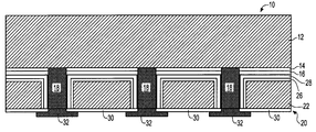
- FIG. 1 is a pictorial representation (through a cross sectional view) illustrating the first wafer and the second wafer employed in the present invention.
- FIG. 2 is a pictorial representation (through a cross sectional view) illustrating the structure after inserting the metal studs disposed on the backside of the first wafer into polyimide coated through vias formed in the second wafer.
- FIG. 3 is a pictorial representation (through a cross sectional view) illustrating the structure of FIG. 2 after attachment and thinning.
- FIG. 4 is a pictorial representation (through a cross sectional view) illustrating the structure of FIG. 3 after backside processing with a polyimide and metal pads.
- FIGS. 5A-5C are pictorial representations (through cross sectional views) illustrating an alternative embodiment wherein the metal studs are not designed to completely bud to the bottom of the through via.
- FIGS. 6A-6D are pictorial representations (through cross sectional views) illustrating yet another embodiment of the present invention wherein an interconnect level is disposed between a first wafer and a second wafer.
- the present invention provides a method of fabricating a reliable metal filled through via for providing a vertical wafer-to-wafer (or chip-to-chip) interconnect structure utilizing a modified transfer and join process wherein alloying of metal studs is avoided.
- the studs consist essentially of a conductive metal which is not an alpha radiation source.
- the method of the present invention includes first providing a first wafer and a second wafer.
- the first wafer has at least one metal stud interconnect to a surface that is typically, but not necessarily always, opposite semiconductor devices and the second wafer includes at least one polyimide coated through via.
- the second wafer may or may not have semiconductor circuitry therein.
- the at least one metal stud of the first wafer is inserted into the at least one polyimide coated through via of the second wafer.
- the now combined first and the second wafers are heated to a temperature that causes the opposing polyimide surfaces to bond and initiate flow to fully encase each of the metal studs.
- a thinning step is then performed on the second wafer to expose a surface of the at least one metal stud positioned within the at least one polyimide coated through via.
- Backside processing with a polyimide coating on a surface of the thinned second wafer and a metal pad on the exposed surface of the at least one metal stud is then preformed.
- FIGS. 1-4 The inventive fabrication process described briefly above is now described in connection with FIGS. 1-4 . It is noted that in these drawings the complete budding of the metal studs to the bottom of the through via is shown. Although this particular embodiment is shown, the present invention also contemplates the embodiment shown in FIGS. 5A-5C . In these drawings and in that embodiment of the present application, the metal studs are designed not to completely bud to the bottom of the through via. In addition, the present invention also contemplates an embodiment in which at least one interconnect level is disposed between the first and second wafers, both of the wafers typically contain semiconductor devices.
- the metal studs are designed to fully bud to the bottom of the through via.
- the term “fully bud” denotes that the metal studs are designed to have a height which ensures that the top surface of the metal studs comes into direct contact with the bottom wall portion of the through via.
- the bottom wall portion is typically lined with a through via liner which is comprised of a dielectric material and a polyimide.
- FIG. 1 illustrates a first step of the present invention in which a first wafer (hereinafter the device wafer) 10 and a second wafer (hereinafter the attachment wafer) 20 are provided.
- the device wafer 10 is the wafer in which at least one semiconductor device (not shown) is formed, while the attachment wafer 20 is a spacer that can be used to absorb alpha radiation from outside sources, such as from C4s and/or ceramic substrates.
- the device wafer 10 includes a first semiconductor substrate 12 which has a patterned first dielectric material 14 located on a surface thereof.
- the patterned first dielectric material 14 is similarly patterned with a polyimide coating 16 or other like bonding material located thereon.
- the device wafer 10 also includes at least one metal stud 18 located on a surface of the first semiconductor substrate 12 which is disposed between the patterned first dielectric material 14 and the polyimide coating 16 .
- the attachment wafer 20 includes a second semiconductor substrate 22 which has at least one through via 24 formed therein. It is noted that the at least one through via 24 does not typically extend entirely through the attachment wafer at this point of the present application.
- the attachment wafer 20 also includes a second dielectric material 26 that lines the exposed surfaces (including bottom and sidewalls) of the at least one through via 24 as well as the surfaces of the second semiconductor substrate 22 located between adjacent through vias.
- a polyimide coating 28 is disposed on the second dielectric material 26 so as to cover the dielectric material that is present on the sidewalls of the at least one through via 24 and the exposed surface of the second substrate 22 adjacent the through vias 24 .
- the device wafer 10 is fabricated utilizing techniques that are well known to those skilled in the art.
- a first dielectric material 14 is applied to a surface of the first semiconductor substrate 12 that is typically opposite the semiconductor devices.
- the first semiconductor substrate 12 comprises any semiconducting material including, but not limited to: Si, Ge, SiGe, SiC, SiGeC, Ga, GaAs, InAs, InP and all other III/V or II/VI compound semiconductors.
- First semiconductor substrate 12 may also comprise an organic semiconductor or a layered semiconductor such as Si/SiGe, silicon-on-insulator (SOI) or a SiGe-on-insulator (SGOI).
- the first semiconductor substrate 12 be composed of a Si-containing semiconductor material, i.e., a semiconductor material that includes silicon.
- the first semiconductor substrate 12 may be doped, undoped or contain doped and undoped regions therein.
- those substrates include top and bottom semiconductor, e.g., Si, layers that are separated at least in part by a buried insulating layer.
- the buried insulating layer includes, for example, a crystalline or non-crystalline oxide, nitride or any combination thereof.
- the buried insulating layer is an oxide.
- the buried insulating layer is formed during initial stages of a layer transfer process or during an ion implantation and annealing process, such as, for example, SIMOX (separation by ion implantation of oxygen).
- the first semiconductor substrate 12 may have a single crystal orientation or alternatively hybrid semiconductor substrates having surface regions of different crystal orientations can also be employed.
- the hybrid substrate allows for fabricating a device upon a specific crystal orientation that enhances the performance of the specific device formed.
- the hybrid substrate allows for providing a structure in which a pFET can be formed on a (110) crystal orientation, while the nFET can be formed on a (100) crystal orientation.
- a hybrid substrate may have SOI-like properties, bulk-like properties or a combination of SOI- and bulk-like properties.
- the first dielectric material 14 is comprised of an oxide, oxynitride, nitride or multilayers thereof. In one embodiment of the present invention, the first dielectric material 14 is comprised of an oxide such as, for example, SiO 2 .
- the first dielectric material 14 is formed by a conventional deposition process such as, for example, chemical vapor deposition (CVD), plasma enhanced chemical vapor deposition (PECVD), atomic layer deposition (ALD), evaporation, chemical solution deposition and other like deposition techniques.
- the first dielectric material 14 may be formed by a thermal process such as, for example, oxidation, nitridation or a combination thereof.
- the thickness of the first dielectric material 14 may vary depending on the technique used in forming the same as well as the type of dielectric material used. Typically, the first dielectric material 14 has a thickness from about 100 to about 2000 nm, with a thickness from about 500 to about 1000 nm being more highly preferred.
- a thermoplastic polyimide (hereinafter just “polyimide”) coating 16 is formed on top of the first dielectric material 14 .
- the polyimide coating 16 is formed utilizing a conventional deposition process including, for example, CVD, PECVD, evaporation and spin-on coating.
- the polyimide coating 16 serves as an adhesive or bonding agent for attaching the device wafer 10 to the attachment wafer 20 .
- the polyimide coating 16 typically has an as-deposited thickness from about 500 to about 10,000 nm, with a thickness from about 1000 to about 3000 nm being even more typical.
- thermoplastic polyimide is a preferred material employed in the present invention since it is malleable, can absorb stress and tends to have a coefficient thermal expansion (CTE) that is greater than the CTE of the semiconductor substrates employed in the present application.
- CTE coefficient thermal expansion
- a patterned photoresist (not shown) is disposed on the either the exposed surface of the first dielectric material 14 (if the polyimide coating is not present) or atop the polyimide coating 16 (if the polyimide coating is present).
- the patterned photoresist is formed by deposition and lithography.
- the deposition step includes a conventional deposition process including, for example, CVD, PECVD, spin-on coating and evaporation.
- the lithographic process includes exposing the applied photoresist to a pattern of radiation and developing the exposed resist utilizing a conventional resist developer.
- the patterned photoresist includes openings that expose the upper surface of either layer 16 or layer 14 .
- the exposed material within these openings is then removed utilizing an etching process. Dry etching (including reactive ion etching, ion beam etching, plasma etching and laser ablation), wet etching or any combination thereof may be utilized.
- the etching provides openings to the first semiconductor substrate 12 in which the at least metal studs 18 are formed. After etching, the patterned photoresist is stripped utilizing a conventional resist developer.
- the metal studs 18 are then formed into the openings utilizing any conventional electroplating process that is well known to those skilled in the art. As is known by those skilled in the art, the metal studs 18 are in contact with either Cu pads or a patterned protective layer that may be present on the device wafer 10 . Neither the Cu pads, nor the patterned protective material is shown in the drawings of the present application.
- the metal studs 18 are comprised of a conductive metal that is not a source of alpha radiation. Examples of conductive metals that are non-alpha radiation source materials include, for example, Cu, Al, W and Au. Of the various conductive metals listed above, it is preferred in some embodiments that the conductive metal be comprised of Cu.
- the height of the metallic studs 18 formed can be designed to either bud to the bottom wall portion of the through via of the attachment substrate, or not to bud to the bottom wall portion of the through via.
- the former embodiment of the present invention is shown in these drawings, while FIGS. 5A-5C show the latter embodiment of the present invention.
- the attachment wafer 20 includes a second semiconductor substrate 22 that has a least one polyimide coated through via.
- the second semiconductor substrate 22 may comprise the same or different semiconductor material as the first semiconductor substrate 12 of the device wafer 10 .
- the second semiconductor substrate 22 is a Si-containing semiconductor substrate.
- At least one through via 24 is then formed into the second semiconductor substrate 22 of the attachment wafer 20 utilizing conventional lithography and etching, both of which have been described above. As previously indicated, the through vias 24 that are formed at this point of the present invention do not typically extend through the entire thickness of the second semiconductor substrate 22 . After through via formation, the resist used in forming the same is stripped utilizing a conventional resist stripping process well known to those skilled in the art.
- a dielectric material 26 is then formed on all exposed surfaces (sidewalls and bottom wall) of the through vias 24 as well as the exposed surface of the second substrate 22 that lies adjacent to said through vias 24 .
- the dielectric material 26 which serves as a through via liner in the attachment wafer 20 may comprise the same or different dielectric material as the first dielectric material 14 of the device wafer.
- the dielectric material 26 be comprised of an oxide such as, for example, SiO 2 . It is noted that the dielectric material 26 can be formed utilizing one of the above mentioned techniques described for the first dielectric material 14 and the thickness of the dielectric material 26 can fall within the ranges mentioned above for the first dielectric material 14 .
- thermoplastic polyimide (hereinafter just “polyimide”) coating 28 is formed on sidewall surfaces of the dielectric material 26 which are located within the at least one through via 24 as well as atop the dielectric material 26 that is located on the portions of the second semiconductor substrate 22 that are adjacent to said through vias 24 .
- the polyimide coating 28 is formed as described above and its thickness is within the ranges mentioned above as well.
- the metal studs 18 bud to the bottom wall portion of the through vias 24 . That is, an upper surface of each of the metal studs 18 comes into intimate contact with the second dielectric material 26 that is present in the through vias 24 .
- the insertion process is performed by applying an external force to at least one of the device wafer 10 or the attachment wafer 20 , or more preferably both wafers.
- This heating step of the present application is performed at a temperature which is capable of achieving polyimide flow and metal stud encasement without damaging the devices that are present in the device wafer 10 .
- flow of the polyimide and encasement of the metal studs, without damaging the devices present in the device wafer 10 is achieved by heating the structure shown in FIG. 2 to a temperature that is less than about 400° C. More typically, the heating step of the present invention is performed at a temperature from about 250° to about 375° C. The time period of this heating step may vary and is dependent on the type of heating technique used.
- the heating step is performed in the presence of an inert ambient and subsequently under pressure.
- inert ambients include He, Ar, Ne, Xe and mixtures thereof such as a mixture of He and Ar.
- an external force may be applied to one or both wafers being transferred and joined together.
- the polyimide coating hardens and entraps the at least one metal studs within the at least one through via of the second wafer.
- the backside of the attachment wafer is then thinned utilizing a conventional planarization process providing the structure shown, for example, in FIG. 3 .
- the thinning of the attachment wafer 20 exposes a surface of the at least one metal stud 18 positioned within said at least one polyimide coated 28 through via 24 .
- Conventional planarization processes that can be used in the present invention for the thinning of the attachment wafer 20 include grinding and/or chemical mechanical polishing (CMP).
- CMP chemical mechanical polishing
- a wet chemical etching process may also be used alone or in conjunction with grinding and/or CMP to thin the attached wafer 20 .
- FIG. 4 shows the structure that is formed after backside processing with another polyimide coating 30 and metal pad 32 .
- the polyimide coating 30 is formed as described above.
- the metal pad 32 which comprises preferably Cu or another like metal is formed by various deposition techniques, lithography and etching.
- the backside polyimide coating 30 assists in filling in any possible remaining voids along the stud sidewalls within the through via.
- the specific geometry of the stud and through via may also be altered to create a “funneled” via (not shown) and a tapered metal stud (also not shown). Process sequence details may also be altered as to specific needs and designs.
- FIGS. 5A-5C illustrates another embodiment of the present application.
- the metal studs 18 are designed to have a height that does not bud into the bottom wall portion of the through via 24 .
- FIG. 5A shows the initial two wafers 10 and 20 , respectively after insertion and joining.
- FIG. 5B shows the structure after thinning of the attachment wafer 20 .
- FIG. 5C shows the structure that is formed after backside processing with another polyimide coating 30 and metal pad 32 .
- the polyimide coating 30 is formed as described above. It is noted that all the materials and processing details for this second embodiment are the same as described above except that the height of the metal studs is designed to be shorter than that used in the embodiment shown in FIGS. 1-4 .
- This particular embodiment illustrates that the height of the initial metal studs 18 used in the present invention is not critical in forming a vertical interconnect structure.
- the second wafer 20 does not include any semiconductor circuitry, i.e., devices, thereon.
- the second wafer 20 merely serves as a spacer between the first wafer 10 and a module (not shown).
- the purpose of the spacer, i.e., second wafer 20 is to absorb any alpha radiation emissions which may be emanating from an intimate and/or neighboring C4 connection, which is used to interconnect the module to the inventive structure.
- FIG. 6A illustrates a first wafer 10 that includes a device region 50 located on a surface of a semiconductor substrate 12 .
- the device region 50 includes one or more semiconductor devices.
- the first wafer 10 also includes metal studs 18 , the first dielectric layer 14 and the polyimide coating 16 .
- Metal contacts 52 are also shown within layers 14 and 16 . The metal contacts 52 are in contact with selective areas of the semiconductor devices, for example, the source/drain regions and gates of a field effect transistor.
- the 6A is fabricated by first forming the semiconductor devices (not shown) on the substrate 12 .
- the first dielectric layer 14 , the polyimide coating 16 and the contact studs 18 are formed as described above, and thereafter, metal contact openings are formed by lithography and etching.
- a contact metal such as Cu, Al, W or AlCu is then formed within the contact opening utilizing a conventional deposition process. The contact metal typically extends outside the contact openings.
- the metal contacts 52 can be fabricated before the metal studs 18 .
- FIG. 6A also shows the presence of a second wafer 20 which includes a second semiconductor substrate 22 which includes a semiconductor device region 54 located on a surface thereof.
- the second wafer 20 also includes at least one through via 24 , second dielectric material 26 , polyimide coating 28 , contact openings 56 and contact pads 58 .
- the contact pads 58 are comprised of conventional metals well known in the art including, for example, Cu.
- the second wafer 20 shown in FIG. 6A is formed by first forming the semiconductor device region 54 and metal contact pads 58 on the second substrate 22 , and thereafter forming the at least one via opening 24 as described above. In some embodiments of the present invention, the aforementioned processing sequence can be reversed. Next, layers 26 and 28 are formed utilizing the techniques described herein above for those layers and thereafter the contact openings 56 are formed by lithography and etching.
- FIG. 6B shows the structure after the two wafers illustrated in FIG. 6A are brought together and heated as described above. It is noted that an interconnect level including the contact pads 58 , metal contacts 52 , and first and second dielectrics 14 and 26 is disposed between the first and second wafers. In this embodiment of the present invention, simultaneous bonding of the contact pads 58 to metal contacts 52 is achieved by the T&J interconnect technique described above, followed with the insertion of metallic studs 18 encasement.
- FIG. 6C shows the structure after the second wafer 20 has been thinned utilizing the above mentioned processing techniques.
- FIG. 6D shows the structure after backside processing with another polyimide coating 30 and a metal pad 32 utilizing the techniques described above.
Landscapes
- Engineering & Computer Science (AREA)
- Microelectronics & Electronic Packaging (AREA)
- Power Engineering (AREA)
- Computer Hardware Design (AREA)
- Physics & Mathematics (AREA)
- Condensed Matter Physics & Semiconductors (AREA)
- General Physics & Mathematics (AREA)
- Manufacturing & Machinery (AREA)
- Internal Circuitry In Semiconductor Integrated Circuit Devices (AREA)
Abstract
A vertical wafer-to-wafer interconnect structure is provided in which a first wafer and a second wafer are mated by way of metal studs that extend from a surface of the first wafer. The metal studs extend from the surface of the first wafer into a corresponding through via of the second wafer. A polyimide coating is present in the through via on mated surfaces of the first and second wafers and on another surface of the second wafer not mated to the first wafer, thus the metal studs provide a continuous metal path from the first wafer through the second wafer. Since only metal studs for the vertical connection are used, no alpha radiation is generated by the metal studs.
Description
The present invention relates to a semiconductor structure and more particularly to a reliable vertical wafer-to-wafer (or chip-to-chip) interconnect structure.
In current semiconductor technology, there is an ongoing trend to increase the performance of a semiconductor chip by shifting from a two-dimensional (2D) chip format to a three-dimensional (3D) chip format. This requires a wafer-to-wafer (or even a chip-to-chip) vertical interconnect.
Vertical interconnects are preferably made by way of a reduced sized solder bump area array interconnect scheme, which is often called a flip-chip solder connection or C4. However, the present lead based C4s are themselves a source of alpha radiation and they typically interfere with the need for a radiation-free interconnect material. Alpha radiation is undesirable since it may introduce soft errors into the semiconductor device. It is noted that not all semiconductor designs are affected by alpha-radiation.
Furthermore, the new lead free C4s that are presently being considered consist mainly of tin (Sn), which itself may be a source of alpha radiation. Hence, these new C4s do not assure the elimination of the alpha radiation issue.
Alternative interconnection can be achieved with a metal stud-to-pad approach. This method, which is described, for example, in U.S. Pat. No. 6,444,560 to Pogge et al., is termed the T&J (transfer and join) approach. A typical T&J interconnect consists of a metal stud (preferably copper, Cu) coated with an alloying metal (typically Sn). The Sn assists the alloying of the metal stud to an opposing metal pad (typically Cu as well). As with the previously mentioned C4 technology, the T&J approach includes Sn which may also be an alpha radiation source.
To accommodate the ability to attach a second semiconductor chip to a first semiconductor chip dictates the need for a vertical through via in the second chip so that there is an electrical path from the first chip through the second chip and to a supporting substrate that is located beneath the second chip. Through via processing has been exercised by a number of semiconductor manufacturers. However, an efficient through via fabrication and through via metal filling has remained a challenge. There is a concern to assure the creation of a smooth vertical through via, rather than some form of corrugated surfaced through via. The latter may initiate metal voids within the metal filled through via which can lead to unacceptable conductivity variations.
In view of the above, there is a need for providing an alternative method for fabricating an improved metal filled through via that overcomes the above mentioned through via concerns as well as avoiding alpha radiation source issues generated by C4s or possible Sn based alloying T&J interconnects.
In a first embodiment of the present invention, there is provided a reliable metal through via that is useful in providing a vertical wafer-to-wafer (or even chip-to-chip) interconnect structure. In accordance with the present invention, the metal filled through via overcomes the above mentioned drawbacks for through via processing. Moreover, the present invention avoids alpha radiation source issues that typically are a concern when C4s or Sn based alloying T&J interconnects are used. The present invention preferably uses a metal stud for the vertical connection, such that no Sn or other alpha radiation generating sources are used in the presence of the metal studs.
In accordance with another embodiment of the present invention, the metal studs are preferably electroplated to the underside of a first semiconductor wafer (i.e., a device wafer) using standard interconnect processing. Each of the studs are then inserted into a corresponding polyimide coated through via of a second semiconductor wafer to form the inventive 3D interconnect structure. In accordance with the present invention, the second semiconductor wafer may or may not have semiconductor circuitry i.e., devices, located thereon. Thus, in accordance with an embodiment of the present invention, the second semiconductor wafer may serve as a spacer that can absorb radiation from an outside source. In yet another embodiment of the present invention, the second semiconductor wafer may have circuitry thereon. In this particular embodiment, at least one interconnect level is typically imposed between the first and second semiconductor wafers. In the foregoing discussion, it is noted that the first and second wafers can also be implied to include first and second semiconductor chips. In such an embodiment of the present invention, the inventive technology can be used in providing a vertical chip-to-chip interconnection.
The polyimide coating mentioned above serves as a bonding material which flows and encases the metal stud during a subsequent heating step. Each stud employed in the present invention is typically, but not necessarily always, designed to bud into the bottom surface of the eventual through via of the second wafer. However, budding is not required in all circumstances. That is, the height of each metallic stud may be slightly shorter than the depth of the eventual through via. Once inserted and then heated, the polyimide flows and fully encases the metal stud to serve as a stress buffer between the metal stud and a dielectric through via liner. The second wafer, once attached, is then thinned with existing planarization processes.
The inventive approach avoids the need for alloying of metal studs, yet creates a continuous metal path from the first wafer through the second wafer.
In general terms, the present invention provides a vertical wafer-to-wafer interconnect structure. More specifically, the inventive vertical wafer-to-wafer interconnect structure includes:
a first wafer and a second wafer which are mated with at least one metal stud that extends from a surface of said first wafer, said at least one metal stud extending from said surface of said first wafer into a corresponding through via of said second wafer, wherein a polyimide coating is present in said through via, on mated surfaces of said first and second wafers and on another surface of said second wafer not mated to said first wafer, and wherein said at least one metal stud provides a continuous metal path from said first wafer through said second wafer.
In another embodiment of the invention, there is provided a method of fabricating a reliable metal filled through via structure for providing vertical wafer-to-wafer interconnection that comprises the steps of:
providing a first wafer and a second wafer, said first wafer having at least one metal stud disposed on a surface thereof and said second wafer including at least one polyimide coated through via;
inserting said at least one metal stud of said first wafer into said at least one polyimide coated through via of said second wafer to provide a combined structure;
heating the combined structure to cause opposing polyimide surfaces to bond and initiate flow to fully encase each metal stud;
thinning the second wafer to expose a surface of the at least one metal stud positioned within said at least one polyimide coated through via; and
forming a patterned polyimide coating on a surface of the thinned second wafer and a metal pad on said exposed surface of said at least one metal stud.
It is noted that when Si-containing wafers are employed, an oxide is generally used and appropriately patterned to protect the wafers prior to other processing, such as, for example, formation of polyimides and metal studs.
In yet another embodiment of the present invention, the method comprises the steps of:
providing a first wafer and a second wafer, said first wafer having at least one Cu stud disposed on a surface thereof and said second wafer including at least one polyimide coated through via;
inserting said at least one Cu stud of said first wafer into said at least one polyimide coated through via of said second wafer to provide a combined structure;
heating the combined structure to cause opposing polyimide surfaces to bond and initiate flow to fully encase each Cu stud;
thinning the second wafer to expose a surface of the at least one Cu stud positioned within said at least one polyimide coated through via; and
forming a patterned polyimide coating on a surface of the thinned second wafer and a Cu pad on said exposed surface of said at least one Cu stud.
The methods of the present invention mentioned above avoid the need for alloying a metal stud to a metal pad, yet they create a continuous metal path from the first wafer (e.g., the device wafer) through the second wafer (attachment wafer or second device wafer).
The preferred embodiment of the present invention, which provides a vertical wafer-to-wafer interconnect structure utilizing only metal studs, will now be described in greater detail by referring to the following discussion and drawings that accompany the present application. It is noted that the drawings of the present application are provided for illustrative purposes, and as such, they are not drawn to scale.
In the following description, numerous specific details are set forth, such as particular structures, components, materials, dimensions, processing steps and techniques, in order to provide a thorough understanding of the present invention. However, it will be appreciated by one of ordinary skill in the art that the invention may be practiced with viable alternative process options without these specific details. In other instances, well-known structures or processing steps have not been described in detail in order to avoid obscuring the invention.
It will be understood that when an element as a layer, region or substrate is referred to as being “on” or “over” another element, it can be directly on the other element or intervening elements may also be present. In contrast, when an element is referred to as being “directly on” or “directly over” another element, there are no intervening elements present. It will also be understood that when an element is referred to as being “beneath” or “under” another element, it can be directly beneath or under the other element, or intervening elements may be present. In contrast, when an element is referred to as being “directly beneath” or “directly under” another element, there are no intervening elements present.
As stated above, the present invention provides a method of fabricating a reliable metal filled through via for providing a vertical wafer-to-wafer (or chip-to-chip) interconnect structure utilizing a modified transfer and join process wherein alloying of metal studs is avoided. In the present invention, the studs consist essentially of a conductive metal which is not an alpha radiation source. In general terms, the method of the present invention includes first providing a first wafer and a second wafer. In accordance with the present invention, the first wafer has at least one metal stud interconnect to a surface that is typically, but not necessarily always, opposite semiconductor devices and the second wafer includes at least one polyimide coated through via. The second wafer may or may not have semiconductor circuitry therein. Next, the at least one metal stud of the first wafer is inserted into the at least one polyimide coated through via of the second wafer. After full insertion, the now combined first and the second wafers are heated to a temperature that causes the opposing polyimide surfaces to bond and initiate flow to fully encase each of the metal studs. A thinning step is then performed on the second wafer to expose a surface of the at least one metal stud positioned within the at least one polyimide coated through via. Backside processing with a polyimide coating on a surface of the thinned second wafer and a metal pad on the exposed surface of the at least one metal stud is then preformed.
The inventive fabrication process described briefly above is now described in connection with FIGS. 1-4 . It is noted that in these drawings the complete budding of the metal studs to the bottom of the through via is shown. Although this particular embodiment is shown, the present invention also contemplates the embodiment shown in FIGS. 5A-5C . In these drawings and in that embodiment of the present application, the metal studs are designed not to completely bud to the bottom of the through via. In addition, the present invention also contemplates an embodiment in which at least one interconnect level is disposed between the first and second wafers, both of the wafers typically contain semiconductor devices.
It is further noted that not all process details are shown in the drawings provided in the present application. For example, the insulating of the surfaces of the first and second wafers with an oxide is not always shown or described herein. Moreover, the formation of devices on the first wafer and optionally the second wafer is not shown or described in the present application. Furthermore, after performing the various processing steps of the present invention, additional processing (not shown or described in greater detail) can be performed on the underside of the second wafer. For example, a patterned oxide is typically formed on the underside of the second wafer prior to forming the contact pads. In some embodiments, wide contact pads are formed around the metal stud to assure good metal contact and larger areas for larger packaging pad attachment needs of the substrate.
Reference is now made to FIGS. 1-4 wherein a first embodiment of the present invention is shown. In this embodiment, the metal studs are designed to fully bud to the bottom of the through via. The term “fully bud” denotes that the metal studs are designed to have a height which ensures that the top surface of the metal studs comes into direct contact with the bottom wall portion of the through via. The bottom wall portion is typically lined with a through via liner which is comprised of a dielectric material and a polyimide.
The attachment wafer 20 includes a second semiconductor substrate 22 which has at least one through via 24 formed therein. It is noted that the at least one through via 24 does not typically extend entirely through the attachment wafer at this point of the present application. The attachment wafer 20 also includes a second dielectric material 26 that lines the exposed surfaces (including bottom and sidewalls) of the at least one through via 24 as well as the surfaces of the second semiconductor substrate 22 located between adjacent through vias. A polyimide coating 28 is disposed on the second dielectric material 26 so as to cover the dielectric material that is present on the sidewalls of the at least one through via 24 and the exposed surface of the second substrate 22 adjacent the through vias 24.
The device wafer 10 is fabricated utilizing techniques that are well known to those skilled in the art. For example, after substrate and device processing, a first dielectric material 14 is applied to a surface of the first semiconductor substrate 12 that is typically opposite the semiconductor devices. The first semiconductor substrate 12 comprises any semiconducting material including, but not limited to: Si, Ge, SiGe, SiC, SiGeC, Ga, GaAs, InAs, InP and all other III/V or II/VI compound semiconductors. First semiconductor substrate 12 may also comprise an organic semiconductor or a layered semiconductor such as Si/SiGe, silicon-on-insulator (SOI) or a SiGe-on-insulator (SGOI). In some embodiments of the present invention, it is preferred that the first semiconductor substrate 12 be composed of a Si-containing semiconductor material, i.e., a semiconductor material that includes silicon. The first semiconductor substrate 12 may be doped, undoped or contain doped and undoped regions therein.
When SOI substrates are employed, those substrates include top and bottom semiconductor, e.g., Si, layers that are separated at least in part by a buried insulating layer. The buried insulating layer includes, for example, a crystalline or non-crystalline oxide, nitride or any combination thereof. Preferably, the buried insulating layer is an oxide. Typically, the buried insulating layer is formed during initial stages of a layer transfer process or during an ion implantation and annealing process, such as, for example, SIMOX (separation by ion implantation of oxygen).
The first semiconductor substrate 12 may have a single crystal orientation or alternatively hybrid semiconductor substrates having surface regions of different crystal orientations can also be employed. The hybrid substrate allows for fabricating a device upon a specific crystal orientation that enhances the performance of the specific device formed. For example, the hybrid substrate allows for providing a structure in which a pFET can be formed on a (110) crystal orientation, while the nFET can be formed on a (100) crystal orientation. When a hybrid substrate is used, it may have SOI-like properties, bulk-like properties or a combination of SOI- and bulk-like properties.
The first dielectric material 14 is comprised of an oxide, oxynitride, nitride or multilayers thereof. In one embodiment of the present invention, the first dielectric material 14 is comprised of an oxide such as, for example, SiO2. The first dielectric material 14 is formed by a conventional deposition process such as, for example, chemical vapor deposition (CVD), plasma enhanced chemical vapor deposition (PECVD), atomic layer deposition (ALD), evaporation, chemical solution deposition and other like deposition techniques. Alternatively, the first dielectric material 14 may be formed by a thermal process such as, for example, oxidation, nitridation or a combination thereof.
The thickness of the first dielectric material 14 may vary depending on the technique used in forming the same as well as the type of dielectric material used. Typically, the first dielectric material 14 has a thickness from about 100 to about 2000 nm, with a thickness from about 500 to about 1000 nm being more highly preferred.
A thermoplastic polyimide (hereinafter just “polyimide”) coating 16 is formed on top of the first dielectric material 14. The polyimide coating 16 is formed utilizing a conventional deposition process including, for example, CVD, PECVD, evaporation and spin-on coating. The polyimide coating 16 serves as an adhesive or bonding agent for attaching the device wafer 10 to the attachment wafer 20. The polyimide coating 16 typically has an as-deposited thickness from about 500 to about 10,000 nm, with a thickness from about 1000 to about 3000 nm being even more typical.
A thermoplastic polyimide is a preferred material employed in the present invention since it is malleable, can absorb stress and tends to have a coefficient thermal expansion (CTE) that is greater than the CTE of the semiconductor substrates employed in the present application.
After forming the first dielectric material 14 and the polyimide coating 16, a patterned photoresist (not shown) is disposed on the either the exposed surface of the first dielectric material 14 (if the polyimide coating is not present) or atop the polyimide coating 16 (if the polyimide coating is present). The patterned photoresist is formed by deposition and lithography. The deposition step includes a conventional deposition process including, for example, CVD, PECVD, spin-on coating and evaporation. The lithographic process includes exposing the applied photoresist to a pattern of radiation and developing the exposed resist utilizing a conventional resist developer. The patterned photoresist includes openings that expose the upper surface of either layer 16 or layer 14. The exposed material within these openings is then removed utilizing an etching process. Dry etching (including reactive ion etching, ion beam etching, plasma etching and laser ablation), wet etching or any combination thereof may be utilized. The etching provides openings to the first semiconductor substrate 12 in which the at least metal studs 18 are formed. After etching, the patterned photoresist is stripped utilizing a conventional resist developer.
The metal studs 18 are then formed into the openings utilizing any conventional electroplating process that is well known to those skilled in the art. As is known by those skilled in the art, the metal studs 18 are in contact with either Cu pads or a patterned protective layer that may be present on the device wafer 10. Neither the Cu pads, nor the patterned protective material is shown in the drawings of the present application. In accordance with the present invention, the metal studs 18 are comprised of a conductive metal that is not a source of alpha radiation. Examples of conductive metals that are non-alpha radiation source materials include, for example, Cu, Al, W and Au. Of the various conductive metals listed above, it is preferred in some embodiments that the conductive metal be comprised of Cu.
The height of the metallic studs 18 formed can be designed to either bud to the bottom wall portion of the through via of the attachment substrate, or not to bud to the bottom wall portion of the through via. The former embodiment of the present invention is shown in these drawings, while FIGS. 5A-5C show the latter embodiment of the present invention.
As stated above and as shown in FIG. 1 , the attachment wafer 20 includes a second semiconductor substrate 22 that has a least one polyimide coated through via. The second semiconductor substrate 22 may comprise the same or different semiconductor material as the first semiconductor substrate 12 of the device wafer 10. Typically, the second semiconductor substrate 22 is a Si-containing semiconductor substrate.
At least one through via 24 is then formed into the second semiconductor substrate 22 of the attachment wafer 20 utilizing conventional lithography and etching, both of which have been described above. As previously indicated, the through vias 24 that are formed at this point of the present invention do not typically extend through the entire thickness of the second semiconductor substrate 22. After through via formation, the resist used in forming the same is stripped utilizing a conventional resist stripping process well known to those skilled in the art.
After providing the at least one through via 24, a dielectric material 26 is then formed on all exposed surfaces (sidewalls and bottom wall) of the through vias 24 as well as the exposed surface of the second substrate 22 that lies adjacent to said through vias 24. The dielectric material 26 which serves as a through via liner in the attachment wafer 20 may comprise the same or different dielectric material as the first dielectric material 14 of the device wafer. In some embodiments, it is preferred that the dielectric material 26 be comprised of an oxide such as, for example, SiO2. It is noted that the dielectric material 26 can be formed utilizing one of the above mentioned techniques described for the first dielectric material 14 and the thickness of the dielectric material 26 can fall within the ranges mentioned above for the first dielectric material 14.
Next, a thermoplastic polyimide (hereinafter just “polyimide”) coating 28 is formed on sidewall surfaces of the dielectric material 26 which are located within the at least one through via 24 as well as atop the dielectric material 26 that is located on the portions of the second semiconductor substrate 22 that are adjacent to said through vias 24. The polyimide coating 28 is formed as described above and its thickness is within the ranges mentioned above as well.
After providing the device wafer 10 and the attachment wafer 20 as described above and as shown in FIG. 1 , these two wafers are brought together such that the at least one metal stud 18 is inserted into the at least one through via 24. The resultant combined structure that is formed after insertion is shown, for example in FIG. 2 . It is noted that in this particular embodiment of the present invention, the metal studs 18 bud to the bottom wall portion of the through vias 24. That is, an upper surface of each of the metal studs 18 comes into intimate contact with the second dielectric material 26 that is present in the through vias 24. The insertion process is performed by applying an external force to at least one of the device wafer 10 or the attachment wafer 20, or more preferably both wafers.
After providing the combined structure shown in FIG. 2 , it is heated to a temperature that causes bonding of the opposing polyimide surfaces and simultaneous flow of the polyimide to fully encase each of the metal studs 18. This heating step of the present application is performed at a temperature which is capable of achieving polyimide flow and metal stud encasement without damaging the devices that are present in the device wafer 10. Specifically, flow of the polyimide and encasement of the metal studs, without damaging the devices present in the device wafer 10, is achieved by heating the structure shown in FIG. 2 to a temperature that is less than about 400° C. More typically, the heating step of the present invention is performed at a temperature from about 250° to about 375° C. The time period of this heating step may vary and is dependent on the type of heating technique used.
In accordance with the present invention, the heating step is performed in the presence of an inert ambient and subsequently under pressure. Examples of inert ambients that can be used in the present invention include He, Ar, Ne, Xe and mixtures thereof such as a mixture of He and Ar.
It is noted that during the heating step an external force may be applied to one or both wafers being transferred and joined together.
After heating, the polyimide coating hardens and entraps the at least one metal studs within the at least one through via of the second wafer.
After joining the two wafers together utilizing the above processing steps, the backside of the attachment wafer is then thinned utilizing a conventional planarization process providing the structure shown, for example, in FIG. 3 . As is shown in FIG. 3 , the thinning of the attachment wafer 20 exposes a surface of the at least one metal stud 18 positioned within said at least one polyimide coated 28 through via 24. Conventional planarization processes that can be used in the present invention for the thinning of the attachment wafer 20 include grinding and/or chemical mechanical polishing (CMP). A wet chemical etching process may also be used alone or in conjunction with grinding and/or CMP to thin the attached wafer 20.
It is noted that the backside polyimide coating 30 assists in filling in any possible remaining voids along the stud sidewalls within the through via. The specific geometry of the stud and through via may also be altered to create a “funneled” via (not shown) and a tapered metal stud (also not shown). Process sequence details may also be altered as to specific needs and designs.
Reference is now made to FIGS. 5A-5C which illustrates another embodiment of the present application. In this embodiment, the metal studs 18 are designed to have a height that does not bud into the bottom wall portion of the through via 24. FIG. 5A shows the initial two wafers 10 and 20, respectively after insertion and joining. FIG. 5B shows the structure after thinning of the attachment wafer 20. FIG. 5C shows the structure that is formed after backside processing with another polyimide coating 30 and metal pad 32. The polyimide coating 30 is formed as described above. It is noted that all the materials and processing details for this second embodiment are the same as described above except that the height of the metal studs is designed to be shorter than that used in the embodiment shown in FIGS. 1-4 . This particular embodiment, illustrates that the height of the initial metal studs 18 used in the present invention is not critical in forming a vertical interconnect structure.
In the above two embodiments, the second wafer 20 does not include any semiconductor circuitry, i.e., devices, thereon. In those embodiments, the second wafer 20 merely serves as a spacer between the first wafer 10 and a module (not shown). The purpose of the spacer, i.e., second wafer 20, is to absorb any alpha radiation emissions which may be emanating from an intimate and/or neighboring C4 connection, which is used to interconnect the module to the inventive structure.
Reference is now made to FIGS. 6A-6D which represent another embodiment of the present application. In this embodiment of the present invention, the invention structure includes at least one interconnect level disposed between first and second wafers which both include semiconductor devices. FIG. 6A illustrates a first wafer 10 that includes a device region 50 located on a surface of a semiconductor substrate 12. The device region 50 includes one or more semiconductor devices. The first wafer 10 also includes metal studs 18, the first dielectric layer 14 and the polyimide coating 16. Metal contacts 52 are also shown within layers 14 and 16. The metal contacts 52 are in contact with selective areas of the semiconductor devices, for example, the source/drain regions and gates of a field effect transistor. The first wafer 10 shown in FIG. 6A is fabricated by first forming the semiconductor devices (not shown) on the substrate 12. Next, the first dielectric layer 14, the polyimide coating 16 and the contact studs 18 are formed as described above, and thereafter, metal contact openings are formed by lithography and etching. A contact metal, such as Cu, Al, W or AlCu is then formed within the contact opening utilizing a conventional deposition process. The contact metal typically extends outside the contact openings. Alternatively, the metal contacts 52 can be fabricated before the metal studs 18.
While the present invention has been particularly shown and described with respect to preferred embodiments thereof, it will be understood by those skilled in the art that the foregoing and other changes in forms, structures, process sequence and details may be made without departing from the spirit and scope of the present invention. It is therefore intended that the present invention not be limited to the exact forms and details described and illustrated, but fall within the scope of the appended claims.
Claims (16)
1. A vertical wafer-to-wafer interconnect structure comprising:
a first wafer and a second wafer which are mated with at least one metal stud that extends from a surface of said first wafer into a corresponding through via of said second wafer, wherein a polyimide coating is present in said through via, on mated surfaces of said first and second wafers and directly on an exposed semiconductor surface of said second wafer not mated to said first wafer, and wherein said polyimide coating that is located directly on the exposed semiconductor surface of said second wafer has at least one edge that is in contact with a vertical edge of said at least one metal stud, and said at least one metal stud provides a continuous metal path from said first wafer through said second wafer.
2. The vertical wafer-to-wafer interconnect structure as recited in claim 1 wherein said first wafer and said second wafer comprise the same or different semiconductor material.
3. The vertical wafer-to-wafer interconnect structure as recited in claim 2 wherein said first wafer and said second wafer each comprise a Si-containing semiconductor.
4. The vertical wafer-to-wafer interconnect structure as recited in claim 1 wherein a dielectric material lines sidewalls of each of said through vias.
5. The vertical wafer-to-wafer interconnect structure as recited in claim 4 wherein said dielectric material is an oxide.
6. The vertical wafer-to-wafer interconnect structure as recited in claim 1 further comprising a metal pad on each exposed surface of said at least one metal stud, said metal pad is located atop a portion of said polyimide coating that is located directly on an exposed semiconductor surface of said second wafer.
7. The vertical wafer-to-wafer interconnect structure as recited in claim 6 wherein said metal pad is comprised of Cu and each of said metal studs are comprised of Cu.
8. The vertical wafer-to-wafer interconnect structure as recited in claim 1 wherein said at least one metal stud comprises a conductive metal selected from the group consisting of Cu, Al, W, and Au.
9. The vertical wafer-to-wafer interconnect structure as recited in claim 8 wherein said conductive metal is Cu.
10. The vertical wafer-to-wafer interconnect structure as recited in claim 1 wherein said first wafer includes semiconductor devices disposed on a surface of a semiconductor substrate.
11. The vertical wafer-to-wafer interconnect structure as recited in claim 1 wherein said second wafer includes semiconductor devices disposed on a surface of another semiconductor substrate, and said first and second wafer are separated by an interconnect level.
12. The vertical wafer-to-wafer interconnect structure as recited in claim 1 wherein said metal studs are electroplated to an underside of said first semiconductor wafer.
13. The vertical wafer-to-wafer interconnect structure as recited in claim 1 wherein each of said studs inserted into said polyimide coated through via of said second wafer from a three-dimensional interconnect structure.
14. The vertical wafer-to-wafer interconnect structure as recited in claim 1 wherein said second wafers absorbs radiation from an outside radiation source.
15. The vertical wafer-to-wafer interconnect structure as recited in claim 1 wherein circuitry is formed on said second wafer.
16. The vertical wafer-to-wafer interconnect structure as recited in claim 1 wherein said first and second wafers are replaced to include first and second semiconductor chips.
Priority Applications (1)
| Application Number | Priority Date | Filing Date | Title |
|---|---|---|---|
| US11/971,581 US7821120B2 (en) | 2006-07-25 | 2008-01-09 | Metal filled through via structure for providing vertical wafer-to-wafer interconnection |
Applications Claiming Priority (2)
| Application Number | Priority Date | Filing Date | Title |
|---|---|---|---|
| US11/459,784 US7344959B1 (en) | 2006-07-25 | 2006-07-25 | Metal filled through via structure for providing vertical wafer-to-wafer interconnection |
| US11/971,581 US7821120B2 (en) | 2006-07-25 | 2008-01-09 | Metal filled through via structure for providing vertical wafer-to-wafer interconnection |
Related Parent Applications (1)
| Application Number | Title | Priority Date | Filing Date |
|---|---|---|---|
| US11/459,784 Division US7344959B1 (en) | 2006-07-25 | 2006-07-25 | Metal filled through via structure for providing vertical wafer-to-wafer interconnection |
Publications (2)
| Publication Number | Publication Date |
|---|---|
| US20080105976A1 US20080105976A1 (en) | 2008-05-08 |
| US7821120B2 true US7821120B2 (en) | 2010-10-26 |
Family
ID=39157563
Family Applications (2)
| Application Number | Title | Priority Date | Filing Date |
|---|---|---|---|
| US11/459,784 Active US7344959B1 (en) | 2006-07-25 | 2006-07-25 | Metal filled through via structure for providing vertical wafer-to-wafer interconnection |
| US11/971,581 Active 2027-05-05 US7821120B2 (en) | 2006-07-25 | 2008-01-09 | Metal filled through via structure for providing vertical wafer-to-wafer interconnection |
Family Applications Before (1)
| Application Number | Title | Priority Date | Filing Date |
|---|---|---|---|
| US11/459,784 Active US7344959B1 (en) | 2006-07-25 | 2006-07-25 | Metal filled through via structure for providing vertical wafer-to-wafer interconnection |
Country Status (7)
| Country | Link |
|---|---|
| US (2) | US7344959B1 (en) |
| EP (1) | EP2047500A4 (en) |
| JP (1) | JP5571381B2 (en) |
| KR (1) | KR101120805B1 (en) |
| CN (1) | CN101496138B (en) |
| TW (1) | TWI417990B (en) |
| WO (1) | WO2008030665A1 (en) |
Cited By (5)
| Publication number | Priority date | Publication date | Assignee | Title |
|---|---|---|---|---|
| US20090315188A1 (en) * | 2007-05-21 | 2009-12-24 | International Business Machines Corporation | Silicon-on-insulator structures for through via in silicon carriers |
| US20100200961A1 (en) * | 2008-05-12 | 2010-08-12 | Satyendra Singh Chauhan | Thru silicon enabled die stacking scheme |
| US9257396B2 (en) * | 2014-05-22 | 2016-02-09 | Invensas Corporation | Compact semiconductor package and related methods |
| US20170179030A1 (en) * | 2012-11-15 | 2017-06-22 | Taiwan Semiconductor Manufacturing Company, Ltd., | Methods of Forming Metal Pad Structures Over TSVS to Reduce Shorting of Upper Metal Layers |
| US9947635B1 (en) * | 2016-10-14 | 2018-04-17 | Advanced Semiconductor Engineering, Inc. | Semiconductor package, interposer and semiconductor process for manufacturing the same |
Families Citing this family (31)
| Publication number | Priority date | Publication date | Assignee | Title |
|---|---|---|---|---|
| US7474005B2 (en) * | 2006-05-31 | 2009-01-06 | Alcatel-Lucent Usa Inc. | Microelectronic element chips |
| US7473577B2 (en) * | 2006-08-11 | 2009-01-06 | International Business Machines Corporation | Integrated chip carrier with compliant interconnect |
| US7696064B2 (en) * | 2007-10-11 | 2010-04-13 | Skyworks Solutions, Inc. | Methods for forming a through via |
| DE102008038946A1 (en) * | 2008-03-10 | 2009-09-24 | Fraunhofer-Gesellschaft zur Förderung der angewandten Forschung e.V. | A method of fabricating a semiconductor-based circuit and semiconductor circuit-based circuit having a three-dimensional circuit topology |
| US8138577B2 (en) * | 2008-03-27 | 2012-03-20 | Hong Kong Applied Science And Technology Research Institute Co., Ltd. | Pulse-laser bonding method for through-silicon-via based stacking of electronic components |
| US8273603B2 (en) | 2008-04-04 | 2012-09-25 | The Charles Stark Draper Laboratory, Inc. | Interposers, electronic modules, and methods for forming the same |
| US8017451B2 (en) | 2008-04-04 | 2011-09-13 | The Charles Stark Draper Laboratory, Inc. | Electronic modules and methods for forming the same |
| US8932906B2 (en) | 2008-08-19 | 2015-01-13 | Taiwan Semiconductor Manufacturing Company, Ltd. | Through silicon via bonding structure |
| US8097525B2 (en) * | 2008-08-29 | 2012-01-17 | International Business Machines Corporation | Vertical through-silicon via for a semiconductor structure |
| US7855455B2 (en) * | 2008-09-26 | 2010-12-21 | International Business Machines Corporation | Lock and key through-via method for wafer level 3 D integration and structures produced |
| US8093099B2 (en) * | 2008-09-26 | 2012-01-10 | International Business Machines Corporation | Lock and key through-via method for wafer level 3D integration and structures produced |
| US9064717B2 (en) * | 2008-09-26 | 2015-06-23 | International Business Machines Corporation | Lock and key through-via method for wafer level 3D integration and structures produced thereby |
| TWI455263B (en) * | 2009-02-16 | 2014-10-01 | Ind Tech Res Inst | Chip package structure and chip package method |
| TWI394247B (en) * | 2010-01-26 | 2013-04-21 | Powertech Technology Inc | Metal post chip connecting device and method free to use soldering material |
| KR101107627B1 (en) * | 2010-02-22 | 2012-01-25 | (주)실리콘화일 | Pad Formation Method of Wafer with Three-Dimensional Structure |
| US8076177B2 (en) * | 2010-05-14 | 2011-12-13 | International Business Machines Corporation | Scalable transfer-join bonding lock-and-key structures |
| US8492260B2 (en) | 2010-08-30 | 2013-07-23 | Semionductor Components Industries, LLC | Processes of forming an electronic device including a feature in a trench |
| FR2964048B1 (en) * | 2010-08-30 | 2012-09-21 | Commissariat Energie Atomique | METHOD FOR PRODUCING A FILM, FOR EXAMPLE MONOCRYSTALLINE, ON A POLYMER SUPPORT |
| JP5763775B2 (en) | 2010-11-02 | 2015-08-12 | エンパイア テクノロジー ディベロップメント エルエルシー | Semiconductor structure with insulated through silicon vias |
| US8299567B2 (en) * | 2010-11-23 | 2012-10-30 | International Business Machines Corporation | Structure of metal e-fuse |
| US8735260B2 (en) * | 2010-12-13 | 2014-05-27 | Taiwan Semiconductor Manufacturing Company, Ltd. | Method to prevent metal pad damage in wafer level package |
| FR2978869A1 (en) * | 2011-08-03 | 2013-02-08 | St Microelectronics Crolles 2 | Method for assembling integrated circuits for forming integrated three-dimensional structure, involves fusing alloy layer at low melting point to form conducting connection between metal lines of two integrated circuits |
| WO2013035337A1 (en) * | 2011-09-09 | 2013-03-14 | 日本特殊陶業株式会社 | Semiconductor module, circuit board |
| US8981533B2 (en) | 2012-09-13 | 2015-03-17 | Semiconductor Components Industries, Llc | Electronic device including a via and a conductive structure, a process of forming the same, and an interposer |
| KR101395235B1 (en) * | 2013-10-31 | 2014-05-16 | (주)실리콘화일 | A image sensor using back illumination photodiode and method of manufacturing the same |
| KR102258739B1 (en) | 2014-03-26 | 2021-06-02 | 삼성전자주식회사 | Semiconductor devices having hybrid stacking structures and methods for fabricating the same |
| US9812354B2 (en) | 2015-05-15 | 2017-11-07 | Semiconductor Components Industries, Llc | Process of forming an electronic device including a material defining a void |
| US10354910B2 (en) * | 2016-05-27 | 2019-07-16 | Raytheon Company | Foundry-agnostic post-processing method for a wafer |
| CN110010478B (en) * | 2018-10-10 | 2021-01-26 | 浙江集迈科微电子有限公司 | Radio frequency micro-system with electromagnetic shielding function and forming process |
| DE102018125901A1 (en) | 2018-10-18 | 2020-04-23 | Osram Opto Semiconductors Gmbh | Method for producing an electronic component, semiconductor chip, electronic component and method for producing a semiconductor chip |
| US11201136B2 (en) | 2020-03-10 | 2021-12-14 | International Business Machines Corporation | High bandwidth module |
Citations (22)
| Publication number | Priority date | Publication date | Assignee | Title |
|---|---|---|---|---|
| US5432999A (en) * | 1992-08-20 | 1995-07-18 | Capps; David F. | Integrated circuit lamination process |
| US5646067A (en) * | 1995-06-05 | 1997-07-08 | Harris Corporation | Method of bonding wafers having vias including conductive material |
| US6444560B1 (en) | 2000-09-26 | 2002-09-03 | International Business Machines Corporation | Process for making fine pitch connections between devices and structure made by the process |
| US6577013B1 (en) * | 2000-09-05 | 2003-06-10 | Amkor Technology, Inc. | Chip size semiconductor packages with stacked dies |
| US20030148590A1 (en) | 2002-02-06 | 2003-08-07 | Kellar Scot A. | Barrier structure against corrosion and contamination in three-dimensional (3-D) wafer-to-wafer vertical stack |
| US20040238933A1 (en) * | 2003-05-27 | 2004-12-02 | Shou-Lung Chen | Stacked package for electronic elements and packaging method thereof |
| US20050051883A1 (en) * | 2003-06-19 | 2005-03-10 | Seiko Epson Corporation | Semiconductor device and method of manufacturing the same, circuit board, and electronic instrument |
| US20050110131A1 (en) | 2003-11-24 | 2005-05-26 | Lee Kevin J. | Vertical wafer stacking using an interposer |
| US6908785B2 (en) * | 2001-12-06 | 2005-06-21 | Samsung Electronics Co., Ltd. | Multi-chip package (MCP) with a conductive bar and method for manufacturing the same |
| US6967162B2 (en) | 2000-07-07 | 2005-11-22 | Chartered Semiconductor Manufacturing Ltd. | Method of copper/copper surface bonding using a conducting polymer for application in IC chip bonding |
| US20050260794A1 (en) | 2002-09-03 | 2005-11-24 | Industrial Technology Research Institute | Method for fabrication of wafer level package incorporating dual compliant layers |
| US20060097357A1 (en) | 2004-11-09 | 2006-05-11 | Renesas Technology Corp. | Semiconductor device having through electrode and method of manufacturing the same |
| US20060121690A1 (en) | 2002-12-20 | 2006-06-08 | Pogge H B | Three-dimensional device fabrication method |
| US20060208331A1 (en) * | 2000-07-11 | 2006-09-21 | Seiko Epson Corporation | Miniature optical element for wireless bonding in an electronic instrument |
| US20060216856A1 (en) * | 2005-03-24 | 2006-09-28 | Memsic, Inc. | Wafer-level package for integrated circuits |
| US20070090490A1 (en) * | 2005-10-26 | 2007-04-26 | Industrial Technology Research Institute | Wafer-to-wafer stack with supporting pedestal |
| US20070117348A1 (en) * | 2005-11-21 | 2007-05-24 | Shriram Ramanathan | 3D integrated circuits using thick metal for backside connections and offset bumps |
| US7279407B2 (en) * | 2004-09-02 | 2007-10-09 | Micron Technology, Inc. | Selective nickel plating of aluminum, copper, and tungsten structures |
| US7385283B2 (en) * | 2006-06-27 | 2008-06-10 | Taiwan Semiconductor Manufacturing Co., Ltd. | Three dimensional integrated circuit and method of making the same |
| US7485968B2 (en) * | 2005-08-11 | 2009-02-03 | Ziptronix, Inc. | 3D IC method and device |
| US7572673B2 (en) * | 2006-01-04 | 2009-08-11 | Samsung Electronics Co., Ltd. | Wafer level package having a stress relief spacer and manufacturing method thereof |
| US7605019B2 (en) * | 2006-07-07 | 2009-10-20 | Qimonda Ag | Semiconductor device with stacked chips and method for manufacturing thereof |
Family Cites Families (3)
| Publication number | Priority date | Publication date | Assignee | Title |
|---|---|---|---|---|
| AU2002368524A1 (en) * | 2002-12-20 | 2004-07-22 | International Business Machines Corporation | Three-dimensional device fabrication method |
| JP4492196B2 (en) * | 2004-04-16 | 2010-06-30 | セイコーエプソン株式会社 | Semiconductor device manufacturing method, circuit board, and electronic apparatus |
| JP3873994B2 (en) | 2004-07-14 | 2007-01-31 | コニカミノルタフォトイメージング株式会社 | Imaging apparatus and image acquisition method |
-
2006
- 2006-07-25 US US11/459,784 patent/US7344959B1/en active Active
-
2007
- 2007-07-11 TW TW096125172A patent/TWI417990B/en not_active IP Right Cessation
- 2007-07-24 EP EP07853503A patent/EP2047500A4/en not_active Ceased
- 2007-07-24 CN CN2007800282364A patent/CN101496138B/en active Active
- 2007-07-24 KR KR1020097000840A patent/KR101120805B1/en active IP Right Grant
- 2007-07-24 JP JP2009521941A patent/JP5571381B2/en active Active
- 2007-07-24 WO PCT/US2007/074170 patent/WO2008030665A1/en active Application Filing
-
2008
- 2008-01-09 US US11/971,581 patent/US7821120B2/en active Active
Patent Citations (23)
| Publication number | Priority date | Publication date | Assignee | Title |
|---|---|---|---|---|
| US5432999A (en) * | 1992-08-20 | 1995-07-18 | Capps; David F. | Integrated circuit lamination process |
| US5646067A (en) * | 1995-06-05 | 1997-07-08 | Harris Corporation | Method of bonding wafers having vias including conductive material |
| US6967162B2 (en) | 2000-07-07 | 2005-11-22 | Chartered Semiconductor Manufacturing Ltd. | Method of copper/copper surface bonding using a conducting polymer for application in IC chip bonding |
| US20060208331A1 (en) * | 2000-07-11 | 2006-09-21 | Seiko Epson Corporation | Miniature optical element for wireless bonding in an electronic instrument |
| US6577013B1 (en) * | 2000-09-05 | 2003-06-10 | Amkor Technology, Inc. | Chip size semiconductor packages with stacked dies |
| US6444560B1 (en) | 2000-09-26 | 2002-09-03 | International Business Machines Corporation | Process for making fine pitch connections between devices and structure made by the process |
| US6908785B2 (en) * | 2001-12-06 | 2005-06-21 | Samsung Electronics Co., Ltd. | Multi-chip package (MCP) with a conductive bar and method for manufacturing the same |
| US20030148590A1 (en) | 2002-02-06 | 2003-08-07 | Kellar Scot A. | Barrier structure against corrosion and contamination in three-dimensional (3-D) wafer-to-wafer vertical stack |
| US20050260794A1 (en) | 2002-09-03 | 2005-11-24 | Industrial Technology Research Institute | Method for fabrication of wafer level package incorporating dual compliant layers |
| US20060121690A1 (en) | 2002-12-20 | 2006-06-08 | Pogge H B | Three-dimensional device fabrication method |
| US7354798B2 (en) * | 2002-12-20 | 2008-04-08 | International Business Machines Corporation | Three-dimensional device fabrication method |
| US20040238933A1 (en) * | 2003-05-27 | 2004-12-02 | Shou-Lung Chen | Stacked package for electronic elements and packaging method thereof |
| US20050051883A1 (en) * | 2003-06-19 | 2005-03-10 | Seiko Epson Corporation | Semiconductor device and method of manufacturing the same, circuit board, and electronic instrument |
| US20050110131A1 (en) | 2003-11-24 | 2005-05-26 | Lee Kevin J. | Vertical wafer stacking using an interposer |
| US7279407B2 (en) * | 2004-09-02 | 2007-10-09 | Micron Technology, Inc. | Selective nickel plating of aluminum, copper, and tungsten structures |
| US20060097357A1 (en) | 2004-11-09 | 2006-05-11 | Renesas Technology Corp. | Semiconductor device having through electrode and method of manufacturing the same |
| US20060216856A1 (en) * | 2005-03-24 | 2006-09-28 | Memsic, Inc. | Wafer-level package for integrated circuits |
| US7485968B2 (en) * | 2005-08-11 | 2009-02-03 | Ziptronix, Inc. | 3D IC method and device |
| US20070090490A1 (en) * | 2005-10-26 | 2007-04-26 | Industrial Technology Research Institute | Wafer-to-wafer stack with supporting pedestal |
| US20070117348A1 (en) * | 2005-11-21 | 2007-05-24 | Shriram Ramanathan | 3D integrated circuits using thick metal for backside connections and offset bumps |
| US7572673B2 (en) * | 2006-01-04 | 2009-08-11 | Samsung Electronics Co., Ltd. | Wafer level package having a stress relief spacer and manufacturing method thereof |
| US7385283B2 (en) * | 2006-06-27 | 2008-06-10 | Taiwan Semiconductor Manufacturing Co., Ltd. | Three dimensional integrated circuit and method of making the same |
| US7605019B2 (en) * | 2006-07-07 | 2009-10-20 | Qimonda Ag | Semiconductor device with stacked chips and method for manufacturing thereof |
Non-Patent Citations (2)
| Title |
|---|
| EP Official Action-Application No. 07853503.6-Jul. 28, 2009. |
| EP Official Action—Application No. 07853503.6—Jul. 28, 2009. |
Cited By (11)
| Publication number | Priority date | Publication date | Assignee | Title |
|---|---|---|---|---|
| US20090315188A1 (en) * | 2007-05-21 | 2009-12-24 | International Business Machines Corporation | Silicon-on-insulator structures for through via in silicon carriers |
| US8198734B2 (en) * | 2007-05-21 | 2012-06-12 | International Business Machines Corporation | Silicon-on-insulator structures for through via in silicon carriers |
| US20100200961A1 (en) * | 2008-05-12 | 2010-08-12 | Satyendra Singh Chauhan | Thru silicon enabled die stacking scheme |
| US20100320575A9 (en) * | 2008-05-12 | 2010-12-23 | Satyendra Singh Chauhan | Thru silicon enabled die stacking scheme |
| US7973416B2 (en) * | 2008-05-12 | 2011-07-05 | Texas Instruments Incorporated | Thru silicon enabled die stacking scheme |
| US20170179030A1 (en) * | 2012-11-15 | 2017-06-22 | Taiwan Semiconductor Manufacturing Company, Ltd., | Methods of Forming Metal Pad Structures Over TSVS to Reduce Shorting of Upper Metal Layers |
| US9984971B2 (en) * | 2012-11-15 | 2018-05-29 | Taiwan Semiconductor Manufacturing Company, Ltd. | Methods of forming metal pad structures over TSVS to reduce shorting of upper metal layers |
| US9257396B2 (en) * | 2014-05-22 | 2016-02-09 | Invensas Corporation | Compact semiconductor package and related methods |
| US9524943B2 (en) | 2014-05-22 | 2016-12-20 | Invensas Corporation | Compact semiconductor package and related methods |
| US9905537B2 (en) | 2014-05-22 | 2018-02-27 | Invensas Corporation | Compact semiconductor package and related methods |
| US9947635B1 (en) * | 2016-10-14 | 2018-04-17 | Advanced Semiconductor Engineering, Inc. | Semiconductor package, interposer and semiconductor process for manufacturing the same |
Also Published As
| Publication number | Publication date |
|---|---|
| CN101496138A (en) | 2009-07-29 |
| WO2008030665A1 (en) | 2008-03-13 |
| KR101120805B1 (en) | 2012-03-26 |
| TWI417990B (en) | 2013-12-01 |
| EP2047500A1 (en) | 2009-04-15 |
| EP2047500A4 (en) | 2009-08-26 |
| US20080105976A1 (en) | 2008-05-08 |
| JP5571381B2 (en) | 2014-08-13 |
| JP2009545174A (en) | 2009-12-17 |
| TW200822284A (en) | 2008-05-16 |
| US7344959B1 (en) | 2008-03-18 |
| CN101496138B (en) | 2011-03-16 |
| KR20090031903A (en) | 2009-03-30 |
Similar Documents
| Publication | Publication Date | Title |
|---|---|---|
| US7821120B2 (en) | Metal filled through via structure for providing vertical wafer-to-wafer interconnection | |
| JP7007496B2 (en) | Multi-layer 3D integration die stack | |
| US10083910B2 (en) | Backside contacts for integrated circuit devices | |
| JP5246831B2 (en) | Electronic device and method of forming the same | |
| TWI543332B (en) | Semiconductor die package and package on package device | |
| US20200251463A1 (en) | Packaging Mechanisms for Dies With Different Sizes of Connectors | |
| TWI254425B (en) | Chip package structure, chip packaging process, chip carrier and manufacturing process thereof | |
| US7535062B2 (en) | Semiconductor device having SOI structure | |
| US20070145367A1 (en) | Three-dimensional integrated circuit structure | |
| US20100090317A1 (en) | Interconnect Structures and Methods | |
| CN111354690A (en) | Method for forming chip packaging structure | |
| CN106935543A (en) | Semiconductor structure and forming method thereof | |
| US11830837B2 (en) | Semiconductor package with air gap | |
| US20230282582A1 (en) | Semiconductor device and semiconductor package including the same | |
| US11694975B2 (en) | Chip package structure | |
| US9437733B2 (en) | Dynamic threshold MOS and methods of forming the same | |
| TWI759063B (en) | Chip package structure and method for forming the same | |
| TW519727B (en) | Semiconductor wafer, semiconductor device and manufacturing method therefor | |
| US11817306B2 (en) | Method for manufacturing semiconductor package with air gap | |
| US20240021470A1 (en) | Semiconductor device and manufacturing method therefor |
Legal Events
| Date | Code | Title | Description |
|---|---|---|---|
| STCF | Information on status: patent grant |
Free format text: PATENTED CASE |
|
| REMI | Maintenance fee reminder mailed | ||
| FPAY | Fee payment |
Year of fee payment: 4 |
|
| SULP | Surcharge for late payment | ||
| MAFP | Maintenance fee payment |
Free format text: PAYMENT OF MAINTENANCE FEE, 8TH YEAR, LARGE ENTITY (ORIGINAL EVENT CODE: M1552) Year of fee payment: 8 |
|
| MAFP | Maintenance fee payment |
Free format text: PAYMENT OF MAINTENANCE FEE, 12TH YEAR, LARGE ENTITY (ORIGINAL EVENT CODE: M1553); ENTITY STATUS OF PATENT OWNER: LARGE ENTITY Year of fee payment: 12 |