US7714546B2 - Step-up regulator with multiple power sources for the controller - Google Patents
Step-up regulator with multiple power sources for the controller Download PDFInfo
- Publication number
- US7714546B2 US7714546B2 US11/705,013 US70501307A US7714546B2 US 7714546 B2 US7714546 B2 US 7714546B2 US 70501307 A US70501307 A US 70501307A US 7714546 B2 US7714546 B2 US 7714546B2
- Authority
- US
- United States
- Prior art keywords
- power supply
- control circuit
- voltage
- output
- switching
- Prior art date
- Legal status (The legal status is an assumption and is not a legal conclusion. Google has not performed a legal analysis and makes no representation as to the accuracy of the status listed.)
- Expired - Fee Related, expires
Links
- 230000010355 oscillation Effects 0.000 claims abstract description 54
- 239000003990 capacitor Substances 0.000 claims description 38
- 230000009191 jumping Effects 0.000 claims description 17
- 230000000087 stabilizing effect Effects 0.000 claims description 5
- 238000000034 method Methods 0.000 abstract description 4
- 238000009499 grossing Methods 0.000 description 24
- 238000010586 diagram Methods 0.000 description 10
- 230000007257 malfunction Effects 0.000 description 3
- 239000000470 constituent Substances 0.000 description 2
- 230000015556 catabolic process Effects 0.000 description 1
- 230000005923 long-lasting effect Effects 0.000 description 1
Images


Classifications
-
- H—ELECTRICITY
- H02—GENERATION; CONVERSION OR DISTRIBUTION OF ELECTRIC POWER
- H02M—APPARATUS FOR CONVERSION BETWEEN AC AND AC, BETWEEN AC AND DC, OR BETWEEN DC AND DC, AND FOR USE WITH MAINS OR SIMILAR POWER SUPPLY SYSTEMS; CONVERSION OF DC OR AC INPUT POWER INTO SURGE OUTPUT POWER; CONTROL OR REGULATION THEREOF
- H02M1/00—Details of apparatus for conversion
- H02M1/36—Means for starting or stopping converters
-
- H—ELECTRICITY
- H02—GENERATION; CONVERSION OR DISTRIBUTION OF ELECTRIC POWER
- H02M—APPARATUS FOR CONVERSION BETWEEN AC AND AC, BETWEEN AC AND DC, OR BETWEEN DC AND DC, AND FOR USE WITH MAINS OR SIMILAR POWER SUPPLY SYSTEMS; CONVERSION OF DC OR AC INPUT POWER INTO SURGE OUTPUT POWER; CONTROL OR REGULATION THEREOF
- H02M3/00—Conversion of DC power input into DC power output
- H02M3/02—Conversion of DC power input into DC power output without intermediate conversion into AC
- H02M3/04—Conversion of DC power input into DC power output without intermediate conversion into AC by static converters
- H02M3/06—Conversion of DC power input into DC power output without intermediate conversion into AC by static converters using resistors or capacitors, e.g. potential divider
- H02M3/07—Conversion of DC power input into DC power output without intermediate conversion into AC by static converters using resistors or capacitors, e.g. potential divider using capacitors charged and discharged alternately by semiconductor devices with control electrode, e.g. charge pumps
- H02M3/073—Charge pumps of the Schenkel-type
-
- H—ELECTRICITY
- H02—GENERATION; CONVERSION OR DISTRIBUTION OF ELECTRIC POWER
- H02M—APPARATUS FOR CONVERSION BETWEEN AC AND AC, BETWEEN AC AND DC, OR BETWEEN DC AND DC, AND FOR USE WITH MAINS OR SIMILAR POWER SUPPLY SYSTEMS; CONVERSION OF DC OR AC INPUT POWER INTO SURGE OUTPUT POWER; CONTROL OR REGULATION THEREOF
- H02M3/00—Conversion of DC power input into DC power output
- H02M3/02—Conversion of DC power input into DC power output without intermediate conversion into AC
- H02M3/04—Conversion of DC power input into DC power output without intermediate conversion into AC by static converters
- H02M3/10—Conversion of DC power input into DC power output without intermediate conversion into AC by static converters using discharge tubes with control electrode or semiconductor devices with control electrode
- H02M3/145—Conversion of DC power input into DC power output without intermediate conversion into AC by static converters using discharge tubes with control electrode or semiconductor devices with control electrode using devices of a triode or transistor type requiring continuous application of a control signal
- H02M3/155—Conversion of DC power input into DC power output without intermediate conversion into AC by static converters using discharge tubes with control electrode or semiconductor devices with control electrode using devices of a triode or transistor type requiring continuous application of a control signal using semiconductor devices only
-
- H—ELECTRICITY
- H02—GENERATION; CONVERSION OR DISTRIBUTION OF ELECTRIC POWER
- H02M—APPARATUS FOR CONVERSION BETWEEN AC AND AC, BETWEEN AC AND DC, OR BETWEEN DC AND DC, AND FOR USE WITH MAINS OR SIMILAR POWER SUPPLY SYSTEMS; CONVERSION OF DC OR AC INPUT POWER INTO SURGE OUTPUT POWER; CONTROL OR REGULATION THEREOF
- H02M1/00—Details of apparatus for conversion
- H02M1/0003—Details of control, feedback or regulation circuits
- H02M1/0006—Arrangements for supplying an adequate voltage to the control circuit of converters
-
- H—ELECTRICITY
- H02—GENERATION; CONVERSION OR DISTRIBUTION OF ELECTRIC POWER
- H02M—APPARATUS FOR CONVERSION BETWEEN AC AND AC, BETWEEN AC AND DC, OR BETWEEN DC AND DC, AND FOR USE WITH MAINS OR SIMILAR POWER SUPPLY SYSTEMS; CONVERSION OF DC OR AC INPUT POWER INTO SURGE OUTPUT POWER; CONTROL OR REGULATION THEREOF
- H02M1/00—Details of apparatus for conversion
- H02M1/0067—Converter structures employing plural converter units, other than for parallel operation of the units on a single load
- H02M1/008—Plural converter units for generating at two or more independent and non-parallel outputs, e.g. systems with plural point of load switching regulators
-
- H—ELECTRICITY
- H03—ELECTRONIC CIRCUITRY
- H03K—PULSE TECHNIQUE
- H03K2217/00—Indexing scheme related to electronic switching or gating, i.e. not by contact-making or -breaking covered by H03K17/00
- H03K2217/0081—Power supply means, e.g. to the switch driver
Definitions
- the present invention relates to switching power supply circuitry used as a power supply source of battery-driven equipment using, for example, a dry cell.
- switching power supply circuitry with a light weight, a small size, and high power efficiency is widely used for battery-driven equipment that uses a DC battery such as a dry cell as a power supply source and includes a portable terminal such as a mobile phone and a notebook computer.
- a DC battery such as a dry cell
- a portable terminal such as a mobile phone and a notebook computer.
- FIG. 11 shows a conventional example described in Japanese Patent Laid-Open No. 2005-312191 and so on.
- this switching power supply circuitry an input voltage VIN applied to an input terminal T 1 is outputted as an output voltage VOUT to an output terminal T 2 through a DC-DC converter 100 .
- a step-up converter is made up of a choke coil 5 , a main switch 6 including an N-channel MOS transistor, a rectifier diode 7 , a rectifier switch 8 , and an output smoothing capacitor 9 .
- the output of the rectifier diode 7 and the rectifier switch 8 is smoothed by the output smoothing capacitor 9 and supplied to a load 10 connected to the output terminal T 2 .
- a ring oscillation circuit 11 is supplied with power from the input terminal T 1 and determines an on/off period when the main switch 6 and the rectifier switch 8 are started through a driving circuit 15 .
- a PWM control circuit 12 is supplied with power from the output terminal T 2 and determines the on/off period of the main switch 6 and the rectifier switch 8 in order to control the output voltage VOUT through a switch 14 and the driving circuit 15 .
- a switching control circuit 13 switches the switch 14 so as to select a driving signal from the ring oscillation circuit 11 upon startup and select a driving signal from the PWM control circuit 12 in a steady state.
- the driving circuit 15 drives the main switch 6 and the rectifier switch 8 in response to the driving signal selected by the switch 14 .
- the switching power supply circuitry is started by applying a voltage not lower than a predetermined voltage to the input terminal T 1 .
- the input voltage VIN is low, to be specific, when an AA battery is connected to the input terminal T 1 to operate the switching power supply circuitry, it is necessary to operate the circuitry with an extremely low input voltage of about 1 V.
- the gate of a CMOS structure has a threshold voltage of nearly 1 V and thus there is little margin from the input voltage VIN of about 1 V.
- a circuit like the PWM control circuit 12 requiring the function of adjusting the on/off time of the driving signal in response to an output feedback signal, simplification for a low power supply voltage operation is limited, making it difficult to design the circuit. In other words, it is difficult to perform temperature compensation for a circuit operation and reduce variations in characteristics, making it difficult to stably control the circuit operation.
- the main switch 6 and the rectifier switch 8 are turned on/off upon startup in response to the driving signal from the ring oscillation circuit 11 supplied with power from the input voltage VIN, and the voltage is increased without feedback control on the output voltage VOUT.
- the ring oscillation circuit 11 inverters of multiple stages are connected like a ring, so that the ring oscillation circuit 11 can be operated with a low power supply voltage.
- a CMOS structure it is only necessary to have a power supply voltage slightly higher than the gate threshold voltage. In other words, an oscillation can be obtained by a power supply voltage of no more than 1 V.
- the switching control circuit 13 switches the switch 14 to select the driving signal from the ring oscillation circuit 11 .
- the switching power supply circuitry does not perform a feedback operation for controlling the output. In this way, a non-feedback boosting operation (hereinafter, will be referred to as “startup oscillation”) is performed by ring oscillation.
- the switching control circuit 13 switches the switch 14 so as to select the driving signal from the PWM control circuit 12 .
- the operation of the switching power supply circuitry shown in FIG. 11 switches from “startup oscillation” to a feedback switching operation (hereinafter, will be referred to as “main oscillation”) using the PWM control circuit 12 supplied with power from the boosted output voltage VOUT.
- main oscillation a feedback switching operation
- the switching power supply circuitry operates such that the output voltage VOUT reaches a target voltage.
- FIG. 12 shows another conventional switching power supply circuitry.
- the switching power supply circuitry is multi-channel control switching power supply circuitry in which an input voltage VIN applied to an input terminal Ti passes through a DC-DC converter 100 to output a plurality of output voltages VOUT 1 , VOUT 2 , VOUT 3 , . . . from output terminals T 2 , T 3 , T 4 , . . . .
- the switching power supply circuitry includes a circuit for outputting the output voltage VOUT 1 (hereinafter, will be abbreviated to CH 1 ), a circuit for outputting the output voltage VOUT 2 (hereinafter, will be abbreviated to CH 2 ), and a circuit for outputting the output voltage VOUT 3 (hereinafter, will be abbreviated to CH 3 ).
- CH 1 is made up of a CH 2 control circuit 16 and a step-down converter including a main switch 17 , a rectifier diode 18 , a choke coil 19 , and an output smoothing capacitor 20 .
- CH 3 is made up of a CH 3 control circuit 21 and a step-up converter including a choke coil 22 , a main switch 23 , a rectifier diode 24 , and an output smoothing capacitor 25 .
- the switching power supply circuitry of FIG. 12 is also started by applying a voltage not lower than a predetermined voltage to the input terminal T 1 .
- the CH 2 control circuit 16 and the CH 3 control circuit 21 are self-biased so as to be supplied with power from the output voltage VOUT 1 of CH 1 , on fear that the control becomes unstable when the input voltage VIN is low.
- switching power supply control is started when the power supply voltage of each control circuit reaches a potential enabling a stable operation, that is, after CH 1 changes from startup oscillation to main oscillation.
- the power supply voltage is the output voltage VOUT 1 of CH 1 in the control circuits of channels other than CH 1 .
- the circuits cannot start until the output voltage VOUT 1 of CH 1 increases to a potential enabling the control circuits of the other channels to stably operate.
- the order of start is restricted such that self-biased CH 1 has to always start first.
- the present invention is designed to solve the conventional problems and has as its object the provision of switching power supply circuitry which can prevent the conventional problems caused by switching from “startup oscillation” to “main oscillation” and can positively start in a multi-channel configuration without being restricted by the order of start.
- the switching power supply circuitry of the present invention includes a step-up converter for switching a DC input voltage by means of a switch element to obtain a DC output voltage boosted from the input voltage, a step-up power supply for a control circuit, the step-up power supply boosting the input voltage and outputting the voltage, and a control circuit supplied with power from the output voltage of the step-up power supply for a control circuit, the control circuit controlling the switch element of the step-up converter when the output voltage of the step-up power supply for a control circuit is not lower than a predetermined operation start voltage.
- control circuit of the step-up converter can be sufficiently supplied with power even when the input voltage is low, so that the power supply circuitry can be positively started.
- the step-up power supply for a control circuit may be configured as a charge pump including an oscillation circuit for generating driving pulses of a predetermined frequency, a plurality of switch elements switching in response to the driving pulses, and at least a single jumping capacitor charged/discharged by the switching of the plurality of switch elements.
- the oscillation circuit is a ring oscillation circuit including inverters of multiple stages connected like a ring, the driving pulses can be generated with a low power supply voltage.
- the step-up power supply for a control circuit may include a stabilizing circuit such as a series regulator for stabilizing the output voltage of the step-up power supply for a control circuit and outputting the voltage.
- a stabilizing circuit such as a series regulator for stabilizing the output voltage of the step-up power supply for a control circuit and outputting the voltage.
- the control circuit may include an error amplifier for generating an error signal of the DC output voltage and a target value and a PWM circuit for generating a driving pulse for controlling the switching operation of the step-up converter in response to the error signal.
- an error amplifier for generating an error signal of the DC output voltage and a target value
- a PWM circuit for generating a driving pulse for controlling the switching operation of the step-up converter in response to the error signal.
- the control circuit may be, when the output voltage is not lower than the predetermined value, supplied with power from the DC output voltage instead of the output voltage of the step-up power supply for a control circuit.
- the step-up power supply for a control circuit may stop operating when the output voltage is not lower than the predetermined value. This configuration can reduce power consumption during a normal operation.
- the second control circuit controlling the DC-DC converter when the voltage of the step-up power supply for a control circuit reaches the predetermined operation start voltage, it is possible to positively start the switching power supply circuitry even in a multi-channel configuration without restricting the order of start.
- the step-up power supply for a control circuit supplies a power supply voltage enabling the control circuit to stably operate, the step-up power supply operating from a low input voltage. It is thus possible to prevent problems caused by switching from startup oscillation to main oscillation in the conventional self-bias method. Therefore, it is possible to positively start the switching power supply circuitry with stability, suppress input rush current and output overshoot or the like upon startup, reduce excessive power consumption, and increase the life of a battery. Also in a multi-channel configuration, the switching power supply circuitry can be positively started without being restricted by the order of start.
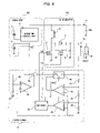
- FIG. 1 is a structural diagram of switching power supply circuitry according to Embodiment 1 of the present invention.
- FIG. 2 is a structural diagram of switching power supply circuitry according to Embodiment 2 of the present invention.
- FIG. 3 is a timing chart showing the start operation of FIG. 1 ;
- FIG. 4 is a circuit block diagram of switching power supply circuitry according to Embodiment 3 of the present invention.
- FIG. 5 is a structural diagram showing a charge pump of Embodiment 3.
- FIG. 6 is a timing chart showing the startup of Embodiment 3.
- FIG. 7 is another structural diagram of the charge pump
- FIG. 8 is a structural diagram of switching power supply circuitry according to Embodiment 4 of the present invention.
- FIG. 9 is a circuit diagram showing power supply to a comparator 47 of Embodiment 4.
- FIG. 10 is a structural diagram of switching power supply circuitry according to Embodiment 5 of the present invention.
- FIG. 11 is a structural diagram of conventional switching power supply circuitry.
- FIG. 12 is a structural diagram of another conventional switching power supply circuitry.
- FIGS. 1 to 10 embodiments of the present invention will now be described below.
- FIGS. 1 and 3 show switching power supply circuitry according to Embodiment 1 of the present invention.
- an input voltage VIN applied to an input terminal T 1 is outputted as an output voltage VOUT to an output terminal T 2 through a DC-DC converter 100 acting as a step-up converter.
- a step-up converter is made up of a choke coil 5 having one end connected to the input terminal T 1 , a main switch 6 including an N-channel MOS transistor, a rectifier diode 7 , a rectifier switch 8 , and an output smoothing capacitor 9 .
- the anode of the rectifier diode 7 , the drain of the main switch 6 , and the drain of the rectifier switch 8 are connected to the other end of the choke coil 5 and the source of the main switch 6 is grounded.
- the output of the rectifier diode 7 and the rectifier switch 8 is smoothed by the output smoothing capacitor 9 and supply to a load 10 connected to the output terminal T 2 .
- the switching power supply circuitry further includes a charge pump 102 supplied with power from the input terminal T 1 and a control circuit 4 operated by power supplied as an output voltage VC from the charge pump 102 .
- the charge pump 102 acts as a step-up power supply for a control circuit for boosting and outputting input voltage.
- the charge pump 102 is made up of a charge pump control circuit 3 , a jumping capacitance 1 for the charge pump, and an output smoothing capacitance 2 for the charge pump.
- the control circuit 4 According to the output voltage VC based on the input voltage VIN of the charge pump 102 , the control circuit 4 outputs control pulses V 6 and V 8 for controlling the gates of the main switch 6 and the rectifier switch 8 .
- FIG. 3 is a timing chart showing the starting operation of the switching power supply circuitry of the present embodiment.
- the switching power supply circuitry is started by supplying the input voltage VIN of FIG. 3(A) .
- the circuit configuration is restricted by a low voltage supplied from an AA battery and it is difficult to perform temperature compensation and reduce variations in characteristics, making it difficult to stably control the circuit operation, whereas the switching power supply circuitry of the present embodiment can achieve a circuit operation even with a low power supply voltage as will be described below:
- the charge pump control circuit 3 operating using the input voltage VIN as a control bias is first operated and started, and the output voltage VC of the charge pump control circuit 3 is monitored by the control circuit 4 as shown FIG. 3(B) .
- the control circuit 4 When it is recognized that the voltage enables a stable operation, the control circuit 4 generates, as shown in FIGS. 3(C) and 3(D) , the control pulses V 6 and V 8 for the gates of the main switch 6 and the rectifier switch 8 at control time T 1 obtained according to the value of bias voltage inputted as the output voltage VC, the control circuit 4 starts the control of a switching power supply for the main switch 6 and the rectifier switch 8 , and the output voltage VOUT is outputted as shown in FIG. 3(E) .
- FIG. 2 shows switching power supply circuitry according to Embodiment 2 of the present invention.
- the switching power supply circuitry is a switching power supply system for performing multi-channel control.
- a charge pump 102 and a control circuit 4 for an output voltage VOUT 1 of a DC-DC converter 100 are similar to those of Embodiment 1. Further, the configurations of CH 2 , CH 3 , . . . are similar to those of FIG. 12 and thus the operations thereof are also similar to those of FIG. 12 . For this reason, the detailed explanation thereof is omitted.
- Embodiment 1 In the multi-channel control of the switching power supply circuitry shown in FIG. 2 , the same operations as Embodiment 1 are performed from the supply of an input voltage VIN to the start of a charge pump control circuit 3 .
- a voltage boosted to a given potential by the charge pump control circuit 3 is monitored by the control circuit of each CH (for example, the control circuit 4 , a CH 2 control circuit 16 , and a CH 3 control circuit 21 ).
- each control circuit recognizes that the voltage enables a stable operation, switching power supply control is started by each control circuit and each output voltage (for example, output voltages VOUT 1 , VOUT 2 , VOUT 3 ) is increased to a desired voltage necessary for equipment to perform stable control.
- the boosted output of a given voltage is supplied as the bias voltage of the control circuit to eliminate the need for the conventional self-bias method in the switching power supply system, the output being obtained by the charge pump control circuit of the charge pump based on the voltage of the input power supply.
- FIGS. 4 to 6 show switching power supply circuitry according to Embodiment 3 of the present invention.
- an input voltage VIN applied to an input terminal T 1 is outputted as an output voltage VOUT to an output terminal T 2 through a DC-DC converter 100 .
- a step-up converter is made up of a choke coil 5 having one end connected to the input terminal T 1 , a main switch 6 including an N-channel MOS transistor, a rectifier diode 7 , a rectifier switch 8 , and an output smoothing capacitor 9 .
- the anode of the rectifier diode 7 , the drain of the main switch 6 , and the drain of the rectifier switch 8 are connected to the other end of the choke coil 5 and the source of the main switch 6 is grounded.
- the output of the rectifier diode 7 and the rectifier switch 8 is smoothed by the output smoothing capacitor 9 and supplied to a load 10 connected to the output terminal T 2 .
- the switching power supply circuitry of Embodiment 3 further includes a charge pump 102 supplied power from the input terminal T 1 and a control circuit 4 operated by power supplied as an output voltage VC from the charge pump 102 .
- the control circuit 4 outputs driving pulses V 6 and V 8 to the gates of the main switch 6 and the rectifier switch 8 such that the output voltage VOUT comes close to a target value.
- the charge pump 102 is made up of a jumping capacitor 1 , an output smoothing capacitor 2 , and a charge pump control circuit 3 supplied with the input voltage VIN.
- FIG. 5 shows a specific configuration of the charge pump 102 .
- the charge pump control circuit 3 of the charge pump 102 is made up of a ring oscillation circuit 30 , an inverter 31 for inverting the output of the ring oscillation circuit 30 by using the output voltage VC of the charge pump 102 as a power supply voltage, a first switch 32 which is supplied with the input voltage VIN from the input terminal T 1 and includes a PMOS transistor driven by the inverter 31 , an inverter 33 for inverting the output of the ring oscillation circuit 30 by using the input voltage VIN from the input terminal T 1 as a power supply voltage, an inverter 34 for inverting the output of the inverter 31 by using the output voltage VC of the charge pump 102 as a power supply voltage, and a second switch 35 which is connected between the source of the first switch 32 and the output smoothing capacitor 2 and includes a PMOS transistor driven by the output of the inverter 34 .
- the jumping capacitor 1 is connected between the source of the first switch 32 and the output of the inverter 33 .
- FIG. 6 is a timing chart showing the starting operation of the switching power supply circuitry of Embodiment 3.
- FIG. 6(A) shows the input voltage VIN
- FIG. 6(B) shows the output voltage VC of the charge pump 102
- FIG. 6(C) shows the driving pulse V 6 to the main switch 6
- FIG. 6(D) shows the driving pulse V 8 to the rectifier switch 8
- FIG. 6(E) shows the output voltage VOUT.
- Embodiment 3 operations upon startup of Embodiment 3 will be described below.
- the switching power supply circuitry of Embodiment 3 is started by applying the input voltage VIN not lower than a predetermined voltage.
- the ring oscillation circuit 30 of the charge pump control circuit 3 operates using the input voltage VIN as a power supply voltage and includes inverters of multiple stages connected like a ring.
- the ring oscillation circuit 30 can operate with a low power supply voltage. In a CMOS structure, it is only necessary to have a power supply voltage slightly higher than the gate threshold voltage. In other words, an oscillation can be obtained by a power supply voltage of no more than 1 V.
- the output of the ring oscillation circuit 30 turns on/off the first switch 32 via the inverter 31 and turns on/off the second switch 35 via the inverter 34 .
- the first switch 32 and the second switch 35 are alternately turned on/off.
- the output of the inverter 33 reaches the ground potential and thus the jumping capacitor 1 is charged from the input voltage VIN.
- the first switch 32 is turned off, the output of the inverter 33 reaches the input voltage VIN.
- the output smoothing capacitor 2 is charged with a voltage equal to the sum of the voltage of the jumping capacitor 1 and the input voltage VIN through the turned-on second switch 35 .
- the power supply voltage of the inverter 33 is the input voltage VIN because the input voltage VIN is outputted from the inverter 33 to increase the voltage of the jumping capacitor 1 to the input voltage VIN.
- the power supply voltage of the inverter 31 and the inverter 34 is the output voltage VC of the charge pump 102 because the gate potentials of the first switch 32 and the second switch 35 serving as PMOS transistors are pulled up to the output voltage VC of the charge pump 102 to positively turn off the switches.
- the output voltage VC is higher than the input voltage VIN.
- the control circuit 4 starts operating.
- the driving pulses V 6 and V 8 are outputted to the main switch 6 and the rectifier switch 8 such that the output voltage VOUT comes close to a target value.
- the main switch 6 and the rectifier switch 8 are alternately turned on/off by the driving pulses from the control circuit 4 .
- the input voltage VIN is applied to the choke coil 5 .
- current passes through the choke coil 5 and energy is accumulated therein.
- the main switch 6 is turned off, the current of the choke coil 5 is applied so as to charge the output smoothing capacitor 9 through the rectifier switch 8 .
- the output voltage VOUT is increased by repeating this operation.
- the output voltage VOUT can be controlled according to the on time of the main switch 6 and the control circuit 4 adjusts the pulse widths of the driving pulses V 6 and V 8 to the main switch 6 and the rectifier switch 8 such that the output voltage VOUT reaches a target value.
- the pulse width (on time) of the driving pulse V 6 of the main switch 6 and the pulse width (off time) of the driving pulse V 8 of the rectifier switch 8 are gradually increased from the start of the operation, which is soft start for suppressing rush current upon startup. Further, the on time of the main switch 6 is included in the off time of the rectifier switch 8 because a dead time is set for preventing through current when the switches are simultaneously turned on. Needless to say, these functions are control functions achieved by supplying a sufficient power supply voltage to the control circuit 4 .
- the output voltage VC is nearly twice the input voltage VIN.
- an excessive power supply voltage may be supplied to the control circuit 4 in response to a high input.
- it is recommendable to provide a voltage regulator circuit such as a series regulator as shown in, for example, FIG. 7 .
- FIG. 7 constituent elements from the ring oscillation circuit 30 to the second switch 35 are identical to those of FIG. 5 .
- FIG. 7 is different from FIG. 5 in that a smoothing capacitor 36 for smoothing the output of the second switch 35 , a power amplifier 37 supplied with power from the smoothing capacitor 36 , and resistors 38 and 39 for dividing the output of the power amplifier 37 are provided.
- the divided voltage of the resistors 38 and 39 is applied to the inverting input terminal ( ⁇ ) of the power amplifier 37
- a reference voltage Vr is applied to the non-inverting input terminal (+) of the power amplifier 37
- the output smoothing capacitor 2 is connected to the output of the power amplifier 37 to output the output voltage VC of the charge pump 102 .
- the power amplifier 37 controls the output voltage VC such that the divided voltage of the resistors 38 and 39 is equal to the reference voltage Vr.
- the output voltage VC is stabilized at a predetermined voltage not larger than twice the input voltage VIN.
- the charge pump 102 operates upon startup to supply the control circuit 4 with a power supply voltage enabling a stable operation.
- the circuitry can smoothly start without malfunctions.
- FIGS. 8 and 9 show switching power supply circuitry according to Embodiment 4 of the present invention.
- the power supply voltage of the control circuit 4 is supplied from the charge pump, whereas in Embodiment 4, the power supply voltage of a control circuit 4 is supplied from an output voltage VOUT when the output voltage VOUT is sufficiently high.
- FIG. 8 constituent elements performing the same operations with the same configurations as those of the switching power supply circuitry of Embodiment 3 of FIG. 4 are indicated by the same reference numerals and the explanation thereof is omitted.
- the switching power supply circuitry of FIG. 8 is different from that of FIG. 4 in the configuration of the control circuit 4 .
- FIG. 4 illustrates a block for outputting the driving pulses V 6 and V 8 to the main switch 6 and the rectifier switch 8
- FIG. 8 illustrates a more specific configuration, including additional functions.
- the control circuit 4 includes resistors 40 and 41 for dividing an output voltage VC of a charge pump, a comparator 42 for comparing the voltage of the junction point of the resistors 40 and 41 with a reference voltage Vr, and a switch 43 switching in response to the output of the comparator 42 .
- the control circuit 4 further includes resistors 44 , 45 and 46 for dividing the output voltage VOUT, a comparator 47 for comparing the voltage of the junction point of the resistors 44 and 45 with the reference voltage Vr, and a switch circuit 48 switching in response to the output of the comparator 47 .
- the switch circuit 48 is supplied with the output of the switch 43 and the output voltage VOUT.
- the switch circuit 48 selects the output of the switch 43 in response to the L-level output of the comparator 47 , selects the output voltage VOUT in response to the H-level output of the comparator 47 , and outputs the selected one of the output and the output voltage VOUT as a power supply voltage VCC in the control circuit.
- the control circuit 4 includes an error amplifier 49 for comparing the voltage of the junction point of the resistors 45 and 46 with the reference voltage Vr and amplifying the voltage, and a pulse-width modulation (PWM) circuit 50 for generating driving pulses V 6 and V 8 having a pulse width corresponding to the output of the error amplifier 49 .
- the error amplifier 49 and the PWM circuit 50 are operated by power supplied from the power supply voltage VCC in the control circuit and the other comparators and switch circuits are operated by power supplied from the output VC of the charge pump.
- the switching power supply circuitry of Embodiment 4 is also started by applying an input voltage VIN not lower than a predetermined voltage.
- the switch circuit 48 selects the output of the switch 43 and outputs the output as the power supply voltage VCC in the control circuit.
- a charge pump 102 is operated by the input voltage VIN serving as a power supply voltage and charges an output smoothing capacitor 2 .
- the PWM circuit 50 outputs the driving pulses V 6 and V 8 in response to the output of the error amplifier 49 for comparing the voltage of the junction point of the resistors 45 and 46 with the reference voltage Vr and amplifying the voltage.
- a main switch 6 and a rectifier switch 8 are alternately turned on/off, current passing through a choke coil 5 charges an output smoothing capacitor 9 , and the output voltage VOUT starts increasing.
- the output of the comparator 47 reaches H level and the switch circuit 48 selects the output voltage VOUT and outputs the voltage as the power supply voltage VCC in the control circuit. Therefore, the error amplifier 49 and the PWM circuit 50 with large current consumption are supplied with power from the output voltage VOUT through the control circuit 4 , reducing the load of power supply in the charge pump 102 .
- the PWM circuit 50 adjusts the pulse widths of the driving pulses V 6 and V 8 in response to the output of the error amplifier 49 .
- the output voltage VOUT is controlled and stabilized such that the voltage of the junction point of the resistors 45 and 46 is equal to the reference voltage Vr.
- the switching power supply circuitry can be smoothly started without causing malfunctions and power consumed in the control circuit 4 is mostly supplied from the output voltage VOUT after startup, thereby reducing the load of power supply in the charge pump 102 . Therefore, the charge pump 102 can be miniaturized on thermal design.
- the charge pump 102 operates all the time, though the load of power supply in the charge pump 102 is reduced.
- the present invention is not limited to this configuration and operation.
- the comparator 42 , the switch 43 , the comparator 47 , the switch circuit 48 and so on are supposed to be supplied with power from the output VC of the charge pump, the power may be supplied from the output voltage VC of the charge pump when the output of the comparator 47 is L level and may be supplied from the output voltage VOUT when the output of the comparator 47 is H level.
- the control circuit 4 only from the output voltage VOUT after startup.
- power consumption can be further reduced by stopping the charge pump 102 after startup.
- a diode 51 is added for, for example, the comparator 47 , so that even when the charge pump 102 is stopped and the output voltage VC of the charge pump 102 is not supplied, power is supplied from the output voltage VOUT through the diode 51 .
- FIG. 10 shows switching power supply circuitry according to Embodiment 5 of the present invention.
- the switching power supply circuitry is configured such that a plurality of output voltages VOUT 1 to VOUT 3 , . . . are outputted from an input voltage VIN through a DC-DC converter.
- FIG. 10 shows a multi-channel control switching power supply including a circuit for outputting the output voltage VOUT 1 , a circuit for outputting the output voltage VOUT 2 , and a circuit for outputting the output voltage VOUT 3 .
- a charge pump, the DC-DC converter for generating the output voltage VOUT 1 , and a control circuit 4 in FIG. 10 are similar in configuration and operation to Embodiment 3 of FIG. 4 and thus the detailed explanation thereof is omitted.
- CH 2 is made up of a CH 2 control circuit 16 and a step-down converter including a main switch 17 , a rectifier diode 18 , a choke coil 19 , and an output smoothing capacitor 20 .
- CH 3 is made up of a CH 3 control circuit 21 and a step-up converter including a choke coil 22 , a main switch 23 , a rectifier diode 24 , and an output smoothing capacitor 25 .
- the CH 2 control circuit 16 and the CH 3 control circuit 21 are supplied with power from an output voltage VC of the charge pump.
- Embodiment 5 the same operations as Embodiment 3 are performed from the supply of an input voltage VIN to the start of a charge pump control circuit 3 .
- the output voltage VC of the charge pump is monitored by the control circuit (for example, the control circuit 4 , the CH 2 control circuit 16 , and the CH 3 control circuit 21 ) of each CH.
- the control circuit for example, the control circuit 4 , the CH 2 control circuit 16 , and the CH 3 control circuit 21 .
- a step-up converter like CH 1 and CH 3 current passes from the input voltage VIN through the choke coils 5 and 22 in response to the on/off of main switches 6 and 23 and charges the output smoothing capacitors 9 and 25 from the rectifier switch 8 and the rectifier diode 24 .
- a step-down converter like CH 2 current passes through the choke coil 19 in response to the on/off of the main switch 17 and charges the output smoothing capacitor 20 .
- the output voltage VC of the charge pump 102 is supplied as a power supply voltage to the control circuit of each channel. It is thus possible to eliminate switching from startup oscillation to main oscillation upon startup of the conventional configuration. Therefore, it is possible to achieve smooth startup without causing malfunctions and remove restrictions on the order of start in the multi-channel configuration. At this point, input rush current, output overshoot and so on upon startup can be suppressed by a control function such as soft start to reduce excessive power consumption, increasing the life of a battery as in Embodiment 3.
- the charge pump 102 of FIG. 5 is made up of the ring oscillation circuit 30 acting as an oscillation circuit for generating driving pulses of a predetermined frequency, the first and second switches 32 and 35 switching in response to the driving pulses, and the single jumping capacitor 1 charged and discharged by the switching of the first and second switches 32 and 35 .
- the single jumping capacitor 1 is charged up to the input voltage VIN and the voltage of the jumping capacitor 1 is added to the input voltage VIN and outputted, so that the output voltage VC of the charge pump 102 is twice the input voltage VIN.
- the output voltage VC of the charge pump 102 can be changed.
- two jumping capacitors having an equal capacitance are provided.
- the two jumping capacitors are connected in series and charged up to the input voltage VIN, and then the two jumping capacitors are connected in parallel.
- a voltage 1.5 times as large as the input voltage VIN can be obtained as the output voltage VC of the charge pump 102 .
- the plurality of jumping capacitors are connected in series or parallel and charged/discharged, so that any given voltage value can be theoretically outputted as the input voltage VIN.
- the switching power supply circuitry of the present invention is useful for electronic equipment using a low-voltage battery.
Landscapes
- Engineering & Computer Science (AREA)
- Power Engineering (AREA)
- Dc-Dc Converters (AREA)
Abstract
Description
- (1) Immediately after switching from “startup oscillation” to “main oscillation”, when the driving pulse from the
PWM control circuit 12 to themain switch 6 has a long pulse width (in other words, the on time of themain switch 6 is long), excessive power is accumulated in thechoke coil 5 during the on period of themain switch 6. Thus overshoot occurs on the output voltage VOUT and the load 10 (for example, a microcomputer) may deteriorate or break in the worst case. Further, excessive rush current is generated on the input and degrades the performance of the battery used for the power supply. - (2) Immediately after switching from “startup oscillation” to “main oscillation”, when the driving pulse from the
PWM control circuit 12 to themain switch 6 has a short pulse width, themain switch 6 is turned off over the period and therectifier switch 8 is turned on over the period with the shortest pulse width. Thus the input voltage VIN and the output voltage VOUT are short-circuited through thechoke coil 5 and therectifier switch 8. For this reason, power (current) accumulated during “startup oscillation” flows back from the output to the power supply, reducing the output voltage VOUT. When the potential of the reduced output voltage VOUT falls below the predetermined value, theswitching control circuit 13 recognizes a startup state again and returns to “startup oscillation”. In this way, a startup failure with repeated “startup oscillation” and “main oscillation” may occur.
Claims (9)
Priority Applications (1)
| Application Number | Priority Date | Filing Date | Title |
|---|---|---|---|
| US12/662,828 US7940031B2 (en) | 2006-03-08 | 2010-05-05 | Switching power supply circuitry |
Applications Claiming Priority (4)
| Application Number | Priority Date | Filing Date | Title |
|---|---|---|---|
| JP2006061945 | 2006-03-08 | ||
| JP2006-061945 | 2006-03-08 | ||
| JP2006332713A JP2007274883A (en) | 2006-03-08 | 2006-12-11 | Switching power supply |
| JP2006-332713 | 2006-12-11 |
Related Child Applications (1)
| Application Number | Title | Priority Date | Filing Date |
|---|---|---|---|
| US12/662,828 Continuation US7940031B2 (en) | 2006-03-08 | 2010-05-05 | Switching power supply circuitry |
Publications (2)
| Publication Number | Publication Date |
|---|---|
| US20070210774A1 US20070210774A1 (en) | 2007-09-13 |
| US7714546B2 true US7714546B2 (en) | 2010-05-11 |
Family
ID=38478288
Family Applications (2)
| Application Number | Title | Priority Date | Filing Date |
|---|---|---|---|
| US11/705,013 Expired - Fee Related US7714546B2 (en) | 2006-03-08 | 2007-02-12 | Step-up regulator with multiple power sources for the controller |
| US12/662,828 Expired - Fee Related US7940031B2 (en) | 2006-03-08 | 2010-05-05 | Switching power supply circuitry |
Family Applications After (1)
| Application Number | Title | Priority Date | Filing Date |
|---|---|---|---|
| US12/662,828 Expired - Fee Related US7940031B2 (en) | 2006-03-08 | 2010-05-05 | Switching power supply circuitry |
Country Status (2)
| Country | Link |
|---|---|
| US (2) | US7714546B2 (en) |
| JP (1) | JP2007274883A (en) |
Cited By (47)
| Publication number | Priority date | Publication date | Assignee | Title |
|---|---|---|---|---|
| US20100277147A1 (en) * | 2006-03-08 | 2010-11-04 | Panasonic Corporation | Switching power supply circuitry |
| US20130028407A1 (en) * | 2011-07-22 | 2013-01-31 | Nec Access Technica, Ltd. | Voltage generation apparatus and voltage generation method |
| US8515361B2 (en) | 2010-04-20 | 2013-08-20 | Rf Micro Devices, Inc. | Frequency correction of a programmable frequency oscillator by propagation delay compensation |
| US8538355B2 (en) | 2010-04-19 | 2013-09-17 | Rf Micro Devices, Inc. | Quadrature power amplifier architecture |
| US8542061B2 (en) | 2010-04-20 | 2013-09-24 | Rf Micro Devices, Inc. | Charge pump based power amplifier envelope power supply and bias power supply |
| US8559898B2 (en) | 2010-04-20 | 2013-10-15 | Rf Micro Devices, Inc. | Embedded RF PA temperature compensating bias transistor |
| US8565694B2 (en) | 2010-04-20 | 2013-10-22 | Rf Micro Devices, Inc. | Split current current digital-to-analog converter (IDAC) for dynamic device switching (DDS) of an RF PA stage |
| US8571492B2 (en) | 2010-04-20 | 2013-10-29 | Rf Micro Devices, Inc. | DC-DC converter current sensing |
| US8699973B2 (en) | 2010-04-20 | 2014-04-15 | Rf Micro Devices, Inc. | PA bias power supply efficiency optimization |
| US8706063B2 (en) | 2010-04-20 | 2014-04-22 | Rf Micro Devices, Inc. | PA envelope power supply undershoot compensation |
| US8712349B2 (en) | 2010-04-20 | 2014-04-29 | Rf Micro Devices, Inc. | Selecting a converter operating mode of a PA envelope power supply |
| US8731498B2 (en) | 2010-04-20 | 2014-05-20 | Rf Micro Devices, Inc. | Temperature correcting an envelope power supply signal for RF PA circuitry |
| US8811921B2 (en) | 2010-04-20 | 2014-08-19 | Rf Micro Devices, Inc. | Independent PA biasing of a driver stage and a final stage |
| US8811920B2 (en) | 2010-04-20 | 2014-08-19 | Rf Micro Devices, Inc. | DC-DC converter semiconductor die structure |
| US8831544B2 (en) | 2010-04-20 | 2014-09-09 | Rf Micro Devices, Inc. | Dynamic device switching (DDS) of an in-phase RF PA stage and a quadrature-phase RF PA stage |
| US8842399B2 (en) | 2010-04-20 | 2014-09-23 | Rf Micro Devices, Inc. | ESD protection of an RF PA semiconductor die using a PA controller semiconductor die |
| US8854019B1 (en) * | 2008-09-25 | 2014-10-07 | Rf Micro Devices, Inc. | Hybrid DC/DC power converter with charge-pump and buck converter |
| US8874050B1 (en) | 2009-05-05 | 2014-10-28 | Rf Micro Devices, Inc. | Saturation correction without using saturation detection and saturation prevention for a power amplifier |
| US8892063B2 (en) | 2010-04-20 | 2014-11-18 | Rf Micro Devices, Inc. | Linear mode and non-linear mode quadrature PA circuitry |
| US8913971B2 (en) | 2010-04-20 | 2014-12-16 | Rf Micro Devices, Inc. | Selecting PA bias levels of RF PA circuitry during a multislot burst |
| US8913967B2 (en) | 2010-04-20 | 2014-12-16 | Rf Micro Devices, Inc. | Feedback based buck timing of a direct current (DC)-DC converter |
| US8942650B2 (en) | 2010-04-20 | 2015-01-27 | Rf Micro Devices, Inc. | RF PA linearity requirements based converter operating mode selection |
| US8942651B2 (en) | 2010-04-20 | 2015-01-27 | Rf Micro Devices, Inc. | Cascaded converged power amplifier |
| US8947157B2 (en) | 2010-04-20 | 2015-02-03 | Rf Micro Devices, Inc. | Voltage multiplier charge pump buck |
| US8958763B2 (en) | 2010-04-20 | 2015-02-17 | Rf Micro Devices, Inc. | PA bias power supply undershoot compensation |
| US8983410B2 (en) | 2010-04-20 | 2015-03-17 | Rf Micro Devices, Inc. | Configurable 2-wire/3-wire serial communications interface |
| US8983407B2 (en) | 2010-04-20 | 2015-03-17 | Rf Micro Devices, Inc. | Selectable PA bias temperature compensation circuitry |
| US8989685B2 (en) | 2010-04-20 | 2015-03-24 | Rf Micro Devices, Inc. | Look-up table based configuration of multi-mode multi-band radio frequency power amplifier circuitry |
| US9008597B2 (en) | 2010-04-20 | 2015-04-14 | Rf Micro Devices, Inc. | Direct current (DC)-DC converter having a multi-stage output filter |
| US9020452B2 (en) | 2010-02-01 | 2015-04-28 | Rf Micro Devices, Inc. | Envelope power supply calibration of a multi-mode radio frequency power amplifier |
| US9030256B2 (en) | 2010-04-20 | 2015-05-12 | Rf Micro Devices, Inc. | Overlay class F choke |
| US9048787B2 (en) | 2010-04-20 | 2015-06-02 | Rf Micro Devices, Inc. | Combined RF detector and RF attenuator with concurrent outputs |
| US9065505B2 (en) | 2012-01-31 | 2015-06-23 | Rf Micro Devices, Inc. | Optimal switching frequency for envelope tracking power supply |
| US9077405B2 (en) | 2010-04-20 | 2015-07-07 | Rf Micro Devices, Inc. | High efficiency path based power amplifier circuitry |
| CN104953799A (en) * | 2014-03-28 | 2015-09-30 | 拉碧斯半导体株式会社 | Voltage booster circuit, semiconductor device, and voltage booster circuit control method |
| US9166471B1 (en) | 2009-03-13 | 2015-10-20 | Rf Micro Devices, Inc. | 3D frequency dithering for DC-to-DC converters used in multi-mode cellular transmitters |
| US9184701B2 (en) | 2010-04-20 | 2015-11-10 | Rf Micro Devices, Inc. | Snubber for a direct current (DC)-DC converter |
| US9214900B2 (en) | 2010-04-20 | 2015-12-15 | Rf Micro Devices, Inc. | Interference reduction between RF communications bands |
| US9214865B2 (en) | 2010-04-20 | 2015-12-15 | Rf Micro Devices, Inc. | Voltage compatible charge pump buck and buck power supplies |
| US9362825B2 (en) | 2010-04-20 | 2016-06-07 | Rf Micro Devices, Inc. | Look-up table based configuration of a DC-DC converter |
| US9553550B2 (en) | 2010-04-20 | 2017-01-24 | Qorvo Us, Inc. | Multiband RF switch ground isolation |
| US9577590B2 (en) | 2010-04-20 | 2017-02-21 | Qorvo Us, Inc. | Dual inductive element charge pump buck and buck power supplies |
| US9900204B2 (en) | 2010-04-20 | 2018-02-20 | Qorvo Us, Inc. | Multiple functional equivalence digital communications interface |
| US10075068B2 (en) * | 2016-11-25 | 2018-09-11 | Ablic Inc. | Power source device |
| US10778104B2 (en) | 2018-09-14 | 2020-09-15 | National Research Council Of Canada | Efficient electricity conversion for harvesting energy from low voltage sources |
| US11387789B2 (en) | 2019-06-05 | 2022-07-12 | Qorvo Us, Inc. | Charge pump tracker circuitry |
| US12003173B2 (en) | 2021-11-09 | 2024-06-04 | Qorvo Us, Inc. | Direct current-to-direct current conversion system |
Families Citing this family (59)
| Publication number | Priority date | Publication date | Assignee | Title |
|---|---|---|---|---|
| JP4996294B2 (en) * | 2007-03-19 | 2012-08-08 | 株式会社リコー | Power supply device, LED device using the power supply device, and electronic apparatus |
| JP5566568B2 (en) * | 2007-03-27 | 2014-08-06 | ピーエスフォー ルクスコ エスエイアールエル | Power supply voltage generation circuit |
| CN101295925B (en) * | 2007-04-24 | 2011-10-05 | 中芯国际集成电路制造(上海)有限公司 | DC/DC converting system |
| JP5406443B2 (en) * | 2007-10-23 | 2014-02-05 | ローム株式会社 | Overvoltage protection circuit |
| JP2009118665A (en) * | 2007-11-07 | 2009-05-28 | Panasonic Corp | Drive circuit, voltage converter, audio system |
| US8212541B2 (en) | 2008-05-08 | 2012-07-03 | Massachusetts Institute Of Technology | Power converter with capacitive energy transfer and fast dynamic response |
| US8498134B2 (en) * | 2008-05-15 | 2013-07-30 | Fraunhofer-Gesellschaft Zur Foerderung Der Angewandten Forschung E.V. | Voltage converter circuit and method for a clock supply of energy to an energy storage |
| US7977920B2 (en) * | 2008-05-15 | 2011-07-12 | Fraunhofer-Gesellschaft Zur Foerderung Der Angewandten Forschung E.V. | Voltage-converter circuit and method for clocked supply of energy to an energy storage |
| TWI400989B (en) * | 2008-05-30 | 2013-07-01 | Green Solution Technology Inc | Light emitting diode driving circuit and controller thereof |
| DE102009045052B4 (en) * | 2008-09-30 | 2013-04-04 | Infineon Technologies Ag | Providing a supply voltage for a drive circuit of a semiconductor switching element |
| TWI399128B (en) * | 2008-10-31 | 2013-06-11 | Advanced Analog Technology Inc | Method and circuit of controlling an led charge pump driving circuit |
| EP2221950A1 (en) * | 2009-02-21 | 2010-08-25 | Braun GmbH | Boost converter with start-up circuit |
| JP5600881B2 (en) * | 2009-03-06 | 2014-10-08 | セイコーエプソン株式会社 | DC-DC converter circuit, electro-optical device, and electronic apparatus |
| JP5418817B2 (en) * | 2009-04-23 | 2014-02-19 | サンケン電気株式会社 | DC-DC converter |
| KR100955090B1 (en) * | 2009-10-12 | 2010-04-28 | (주)이미지스테크놀로지 | A method for generating high power voltage correlated with load driving signal and generating circuit thereof |
| KR101634377B1 (en) * | 2009-10-26 | 2016-06-28 | 삼성전자주식회사 | Circuit and method for generating internal voltage, and semiconductor device having same |
| US10389235B2 (en) | 2011-05-05 | 2019-08-20 | Psemi Corporation | Power converter |
| EP2475086B1 (en) * | 2011-01-11 | 2016-08-24 | OSRAM GmbH | Power supply device, for example for light sources |
| EP4318909A3 (en) | 2011-05-05 | 2024-03-06 | PSEMI Corporation | Dc-dc converter with modular stages |
| US10680515B2 (en) | 2011-05-05 | 2020-06-09 | Psemi Corporation | Power converters with modular stages |
| US9882471B2 (en) | 2011-05-05 | 2018-01-30 | Peregrine Semiconductor Corporation | DC-DC converter with modular stages |
| KR101897051B1 (en) | 2011-09-21 | 2018-10-29 | 엘지이노텍 주식회사 | boosting power system and method thereof |
| KR101786587B1 (en) * | 2011-10-14 | 2017-10-19 | 삼성전자주식회사 | Apparatus and method for modulating supply of power amplifier |
| US8743553B2 (en) | 2011-10-18 | 2014-06-03 | Arctic Sand Technologies, Inc. | Power converters with integrated capacitors |
| US8723491B2 (en) | 2011-12-19 | 2014-05-13 | Arctic Sand Technologies, Inc. | Control of power converters with capacitive energy transfer |
| US8693224B1 (en) | 2012-11-26 | 2014-04-08 | Arctic Sand Technologies Inc. | Pump capacitor configuration for switched capacitor circuits |
| US9847712B2 (en) | 2013-03-15 | 2017-12-19 | Peregrine Semiconductor Corporation | Fault control for switched capacitor power converter |
| US8619445B1 (en) | 2013-03-15 | 2013-12-31 | Arctic Sand Technologies, Inc. | Protection of switched capacitor power converter |
| US8724353B1 (en) | 2013-03-15 | 2014-05-13 | Arctic Sand Technologies, Inc. | Efficient gate drivers for switched capacitor converters |
| US9203299B2 (en) | 2013-03-15 | 2015-12-01 | Artic Sand Technologies, Inc. | Controller-driven reconfiguration of switched-capacitor power converter |
| US9660520B2 (en) | 2013-04-09 | 2017-05-23 | Massachusetts Institute Of Technology | Method and apparatus to provide power conversion with high power factor |
| US20140354258A1 (en) * | 2013-05-30 | 2014-12-04 | Silicon Laboratories Inc. | Supply voltage circuit |
| US9106134B2 (en) * | 2013-06-21 | 2015-08-11 | O2Micro, Inc. | Power transfer devices |
| US9742266B2 (en) | 2013-09-16 | 2017-08-22 | Arctic Sand Technologies, Inc. | Charge pump timing control |
| US9041459B2 (en) | 2013-09-16 | 2015-05-26 | Arctic Sand Technologies, Inc. | Partial adiabatic conversion |
| US9825545B2 (en) | 2013-10-29 | 2017-11-21 | Massachusetts Institute Of Technology | Switched-capacitor split drive transformer power conversion circuit |
| US9385600B2 (en) * | 2013-11-22 | 2016-07-05 | Texas Instruments Incorporated | Low-loss step-up and step-down voltage converter |
| KR102320320B1 (en) | 2014-03-14 | 2021-11-01 | 아크틱 샌드 테크놀로지스, 인크. | Charge balanced charge pump control |
| US9887622B2 (en) | 2014-03-14 | 2018-02-06 | Peregrine Semiconductor Corporation | Charge pump stability control |
| US10693368B2 (en) | 2014-03-14 | 2020-06-23 | Psemi Corporation | Charge pump stability control |
| US10075064B2 (en) | 2014-07-03 | 2018-09-11 | Massachusetts Institute Of Technology | High-frequency, high density power factor correction conversion for universal input grid interface |
| KR102688244B1 (en) | 2015-03-13 | 2024-07-24 | 피세미 코포레이션 | DC-DC transformer with an inductor to facilitate charge transport between insulating capacitors |
| US20180205315A1 (en) | 2015-07-08 | 2018-07-19 | Psemi Corporation | Switched-capacitor power converters |
| JP2017055531A (en) * | 2015-09-08 | 2017-03-16 | 株式会社東芝 | Boost converter |
| CN205922901U (en) * | 2016-08-10 | 2017-02-08 | 卓尔悦欧洲控股有限公司 | Electron cigarette drive circuit and electron cigarette |
| CN205987969U (en) * | 2016-08-17 | 2017-03-01 | 卓尔悦欧洲控股有限公司 | Electronic cigarette and its power supply circuits |
| JP2018098977A (en) * | 2016-12-15 | 2018-06-21 | エイブリック株式会社 | Step-up type dc-dc converter and method for using the same |
| KR101815859B1 (en) * | 2017-01-04 | 2018-01-08 | 한국과학기술원 | Power management device |
| DE102017204044A1 (en) * | 2017-02-14 | 2018-08-16 | Ellenberger & Poensgen Gmbh | Method and voltage multiplier for converting an input voltage and separation circuit |
| JP2019115189A (en) | 2017-12-25 | 2019-07-11 | 旭化成エレクトロニクス株式会社 | Power supply apparatus |
| JP6962851B2 (en) * | 2018-03-30 | 2021-11-05 | エイブリック株式会社 | Power supply circuit |
| US10686367B1 (en) | 2019-03-04 | 2020-06-16 | Psemi Corporation | Apparatus and method for efficient shutdown of adiabatic charge pumps |
| US10845833B1 (en) * | 2019-10-15 | 2020-11-24 | Texas Instruments Incorporated | Method and system for buck converter current re-use for minimum switching frequency pulse-skip operation |
| US11233450B2 (en) | 2020-05-11 | 2022-01-25 | Hamilton Sundstrand Corporation | Multi-output power supply with dual power-on control |
| US12027979B2 (en) | 2020-06-10 | 2024-07-02 | Apple Inc. | Battery path impedance compensation |
| WO2021253122A1 (en) * | 2020-06-16 | 2021-12-23 | National Research Council Of Canada | Synchronous rectification to improve efficiency of electricity conversion for harvesting energy from low voltage sources |
| TWI764795B (en) * | 2021-04-09 | 2022-05-11 | 立錡科技股份有限公司 | Flyback power converter and switched capacitor converter circuit thereof |
| US11888393B2 (en) * | 2021-11-30 | 2024-01-30 | Texas Instruments Incorporated | Multiphase controller communication |
| JP2024137243A (en) * | 2023-03-24 | 2024-10-07 | エイブリック株式会社 | DC-DC Converter |
Citations (4)
| Publication number | Priority date | Publication date | Assignee | Title |
|---|---|---|---|---|
| US5247239A (en) * | 1991-08-22 | 1993-09-21 | Motorola, Inc. | Dual dc/dc voltage converter power system |
| US5659241A (en) * | 1994-12-28 | 1997-08-19 | Rohm Co., Ltd. | DC/DC converter and audio device incorporating the same |
| US6903535B2 (en) * | 2002-04-16 | 2005-06-07 | Arques Technology, Inc. | Biasing system and method for low voltage DC—DC converters with built-in N-FETs |
| JP2005312191A (en) | 2004-04-22 | 2005-11-04 | Matsushita Electric Ind Co Ltd | Switching power supply |
Family Cites Families (5)
| Publication number | Priority date | Publication date | Assignee | Title |
|---|---|---|---|---|
| JP4094487B2 (en) * | 2003-05-21 | 2008-06-04 | ローム株式会社 | Power supply for positive / negative output voltage |
| US7098633B1 (en) * | 2005-07-15 | 2006-08-29 | Analog Devices, Inc. | Boost converter with series switch |
| JP2007274883A (en) * | 2006-03-08 | 2007-10-18 | Matsushita Electric Ind Co Ltd | Switching power supply |
| US7688052B2 (en) * | 2006-12-05 | 2010-03-30 | Semiconductor Components Industries, Llc | Charge pump circuit and method therefor |
| US7782027B2 (en) * | 2006-12-30 | 2010-08-24 | Advanced Analogic Technologies, Inc. | High-efficiency DC/DC voltage converter including down inductive switching pre-regulator and capacitive switching post-converter |
-
2006
- 2006-12-11 JP JP2006332713A patent/JP2007274883A/en not_active Withdrawn
-
2007
- 2007-02-12 US US11/705,013 patent/US7714546B2/en not_active Expired - Fee Related
-
2010
- 2010-05-05 US US12/662,828 patent/US7940031B2/en not_active Expired - Fee Related
Patent Citations (4)
| Publication number | Priority date | Publication date | Assignee | Title |
|---|---|---|---|---|
| US5247239A (en) * | 1991-08-22 | 1993-09-21 | Motorola, Inc. | Dual dc/dc voltage converter power system |
| US5659241A (en) * | 1994-12-28 | 1997-08-19 | Rohm Co., Ltd. | DC/DC converter and audio device incorporating the same |
| US6903535B2 (en) * | 2002-04-16 | 2005-06-07 | Arques Technology, Inc. | Biasing system and method for low voltage DC—DC converters with built-in N-FETs |
| JP2005312191A (en) | 2004-04-22 | 2005-11-04 | Matsushita Electric Ind Co Ltd | Switching power supply |
Cited By (58)
| Publication number | Priority date | Publication date | Assignee | Title |
|---|---|---|---|---|
| US7940031B2 (en) * | 2006-03-08 | 2011-05-10 | Panasonic Corporation | Switching power supply circuitry |
| US20100277147A1 (en) * | 2006-03-08 | 2010-11-04 | Panasonic Corporation | Switching power supply circuitry |
| US8854019B1 (en) * | 2008-09-25 | 2014-10-07 | Rf Micro Devices, Inc. | Hybrid DC/DC power converter with charge-pump and buck converter |
| US9166471B1 (en) | 2009-03-13 | 2015-10-20 | Rf Micro Devices, Inc. | 3D frequency dithering for DC-to-DC converters used in multi-mode cellular transmitters |
| US8874050B1 (en) | 2009-05-05 | 2014-10-28 | Rf Micro Devices, Inc. | Saturation correction without using saturation detection and saturation prevention for a power amplifier |
| US9197182B2 (en) | 2010-02-01 | 2015-11-24 | Rf Micro Devices, Inc. | Envelope power supply calibration of a multi-mode radio frequency power amplifier |
| US9031522B2 (en) | 2010-02-01 | 2015-05-12 | Rf Micro Devices, Inc. | Envelope power supply calibration of a multi-mode radio frequency power amplifier |
| US9020452B2 (en) | 2010-02-01 | 2015-04-28 | Rf Micro Devices, Inc. | Envelope power supply calibration of a multi-mode radio frequency power amplifier |
| US8983409B2 (en) | 2010-04-19 | 2015-03-17 | Rf Micro Devices, Inc. | Auto configurable 2/3 wire serial interface |
| US8538355B2 (en) | 2010-04-19 | 2013-09-17 | Rf Micro Devices, Inc. | Quadrature power amplifier architecture |
| US8983407B2 (en) | 2010-04-20 | 2015-03-17 | Rf Micro Devices, Inc. | Selectable PA bias temperature compensation circuitry |
| US9362825B2 (en) | 2010-04-20 | 2016-06-07 | Rf Micro Devices, Inc. | Look-up table based configuration of a DC-DC converter |
| US8712349B2 (en) | 2010-04-20 | 2014-04-29 | Rf Micro Devices, Inc. | Selecting a converter operating mode of a PA envelope power supply |
| US8731498B2 (en) | 2010-04-20 | 2014-05-20 | Rf Micro Devices, Inc. | Temperature correcting an envelope power supply signal for RF PA circuitry |
| US8811921B2 (en) | 2010-04-20 | 2014-08-19 | Rf Micro Devices, Inc. | Independent PA biasing of a driver stage and a final stage |
| US8811920B2 (en) | 2010-04-20 | 2014-08-19 | Rf Micro Devices, Inc. | DC-DC converter semiconductor die structure |
| US8831544B2 (en) | 2010-04-20 | 2014-09-09 | Rf Micro Devices, Inc. | Dynamic device switching (DDS) of an in-phase RF PA stage and a quadrature-phase RF PA stage |
| US8842399B2 (en) | 2010-04-20 | 2014-09-23 | Rf Micro Devices, Inc. | ESD protection of an RF PA semiconductor die using a PA controller semiconductor die |
| US8892063B2 (en) | 2010-04-20 | 2014-11-18 | Rf Micro Devices, Inc. | Linear mode and non-linear mode quadrature PA circuitry |
| US8913971B2 (en) | 2010-04-20 | 2014-12-16 | Rf Micro Devices, Inc. | Selecting PA bias levels of RF PA circuitry during a multislot burst |
| US8913967B2 (en) | 2010-04-20 | 2014-12-16 | Rf Micro Devices, Inc. | Feedback based buck timing of a direct current (DC)-DC converter |
| US8942650B2 (en) | 2010-04-20 | 2015-01-27 | Rf Micro Devices, Inc. | RF PA linearity requirements based converter operating mode selection |
| US9900204B2 (en) | 2010-04-20 | 2018-02-20 | Qorvo Us, Inc. | Multiple functional equivalence digital communications interface |
| US8942651B2 (en) | 2010-04-20 | 2015-01-27 | Rf Micro Devices, Inc. | Cascaded converged power amplifier |
| US8947157B2 (en) | 2010-04-20 | 2015-02-03 | Rf Micro Devices, Inc. | Voltage multiplier charge pump buck |
| US8958763B2 (en) | 2010-04-20 | 2015-02-17 | Rf Micro Devices, Inc. | PA bias power supply undershoot compensation |
| US8699973B2 (en) | 2010-04-20 | 2014-04-15 | Rf Micro Devices, Inc. | PA bias power supply efficiency optimization |
| US8983410B2 (en) | 2010-04-20 | 2015-03-17 | Rf Micro Devices, Inc. | Configurable 2-wire/3-wire serial communications interface |
| US8571492B2 (en) | 2010-04-20 | 2013-10-29 | Rf Micro Devices, Inc. | DC-DC converter current sensing |
| US8989685B2 (en) | 2010-04-20 | 2015-03-24 | Rf Micro Devices, Inc. | Look-up table based configuration of multi-mode multi-band radio frequency power amplifier circuitry |
| US9008597B2 (en) | 2010-04-20 | 2015-04-14 | Rf Micro Devices, Inc. | Direct current (DC)-DC converter having a multi-stage output filter |
| US8565694B2 (en) | 2010-04-20 | 2013-10-22 | Rf Micro Devices, Inc. | Split current current digital-to-analog converter (IDAC) for dynamic device switching (DDS) of an RF PA stage |
| US8559898B2 (en) | 2010-04-20 | 2013-10-15 | Rf Micro Devices, Inc. | Embedded RF PA temperature compensating bias transistor |
| US9030256B2 (en) | 2010-04-20 | 2015-05-12 | Rf Micro Devices, Inc. | Overlay class F choke |
| US9048787B2 (en) | 2010-04-20 | 2015-06-02 | Rf Micro Devices, Inc. | Combined RF detector and RF attenuator with concurrent outputs |
| US9722492B2 (en) | 2010-04-20 | 2017-08-01 | Qorvo Us, Inc. | Direct current (DC)-DC converter having a multi-stage output filter |
| US9577590B2 (en) | 2010-04-20 | 2017-02-21 | Qorvo Us, Inc. | Dual inductive element charge pump buck and buck power supplies |
| US9077405B2 (en) | 2010-04-20 | 2015-07-07 | Rf Micro Devices, Inc. | High efficiency path based power amplifier circuitry |
| US9553550B2 (en) | 2010-04-20 | 2017-01-24 | Qorvo Us, Inc. | Multiband RF switch ground isolation |
| US8542061B2 (en) | 2010-04-20 | 2013-09-24 | Rf Micro Devices, Inc. | Charge pump based power amplifier envelope power supply and bias power supply |
| US9184701B2 (en) | 2010-04-20 | 2015-11-10 | Rf Micro Devices, Inc. | Snubber for a direct current (DC)-DC converter |
| US8515361B2 (en) | 2010-04-20 | 2013-08-20 | Rf Micro Devices, Inc. | Frequency correction of a programmable frequency oscillator by propagation delay compensation |
| US9214900B2 (en) | 2010-04-20 | 2015-12-15 | Rf Micro Devices, Inc. | Interference reduction between RF communications bands |
| US9214865B2 (en) | 2010-04-20 | 2015-12-15 | Rf Micro Devices, Inc. | Voltage compatible charge pump buck and buck power supplies |
| US8706063B2 (en) | 2010-04-20 | 2014-04-22 | Rf Micro Devices, Inc. | PA envelope power supply undershoot compensation |
| US8917865B2 (en) * | 2011-07-22 | 2014-12-23 | Nec Accesstechnica, Ltd. | Voltage generation apparatus and voltage generation method |
| US20130028407A1 (en) * | 2011-07-22 | 2013-01-31 | Nec Access Technica, Ltd. | Voltage generation apparatus and voltage generation method |
| US9065505B2 (en) | 2012-01-31 | 2015-06-23 | Rf Micro Devices, Inc. | Optimal switching frequency for envelope tracking power supply |
| CN104953799B (en) * | 2014-03-28 | 2019-05-03 | 拉碧斯半导体株式会社 | The control method of booster circuit, semiconductor device and booster circuit |
| CN104953799A (en) * | 2014-03-28 | 2015-09-30 | 拉碧斯半导体株式会社 | Voltage booster circuit, semiconductor device, and voltage booster circuit control method |
| US10447155B2 (en) | 2016-11-25 | 2019-10-15 | Ablic Inc. | Power source device |
| US10075068B2 (en) * | 2016-11-25 | 2018-09-11 | Ablic Inc. | Power source device |
| TWI748000B (en) * | 2016-11-25 | 2021-12-01 | 日商艾普凌科有限公司 | Power source device |
| US10778104B2 (en) | 2018-09-14 | 2020-09-15 | National Research Council Of Canada | Efficient electricity conversion for harvesting energy from low voltage sources |
| TWI794540B (en) * | 2018-09-14 | 2023-03-01 | 加拿大國家研究院 | Dc-dc converter, power supply, and method of converting low voltage dc input to higher voltage dc output |
| US11387789B2 (en) | 2019-06-05 | 2022-07-12 | Qorvo Us, Inc. | Charge pump tracker circuitry |
| US11742804B2 (en) | 2019-06-05 | 2023-08-29 | Qorvo Us, Inc. | Charge pump tracker circuitry |
| US12003173B2 (en) | 2021-11-09 | 2024-06-04 | Qorvo Us, Inc. | Direct current-to-direct current conversion system |
Also Published As
| Publication number | Publication date |
|---|---|
| US20100277147A1 (en) | 2010-11-04 |
| JP2007274883A (en) | 2007-10-18 |
| US7940031B2 (en) | 2011-05-10 |
| US20070210774A1 (en) | 2007-09-13 |
Similar Documents
| Publication | Publication Date | Title |
|---|---|---|
| US7714546B2 (en) | Step-up regulator with multiple power sources for the controller | |
| US7498793B2 (en) | Current-mode DC-to-DC-converter | |
| US7868602B2 (en) | Power supply device and electronic appliance therewith | |
| US7944191B2 (en) | Switching regulator with automatic multi mode conversion | |
| KR100927882B1 (en) | Control method of DC-DC converter and DC-DC converter | |
| US8040701B2 (en) | Control circuit and method for charge pump circuit with pulse modulation | |
| US8193853B2 (en) | Efficiency and thermal improvement of a charge pump by mixing different input voltages | |
| US7528589B2 (en) | Step-up DC/DC converter and electronic appliance therewith | |
| CN100514813C (en) | DC-DC converter and dc-dc converter control method | |
| US7893667B2 (en) | PWM power supply apparatus having a controlled duty ratio without causing overall system oscillation | |
| JP4347249B2 (en) | DC-DC converter, control circuit for DC-DC converter, and control method for DC-DC converter | |
| US11038420B2 (en) | Charge pump transient response optimization by controlled flying capacitor discharge during bypass to switching mode transition | |
| CN101133544A (en) | Output device and electronic device having the same | |
| JP5951358B2 (en) | Charging control circuit and charging circuit | |
| JP4762722B2 (en) | Power supply device and electronic apparatus equipped with the same | |
| US6307359B1 (en) | DC-DC converter powered by doubled output voltage | |
| US20060028854A1 (en) | Charge pump circuit | |
| JP4236602B2 (en) | Switching power supply circuit and electronic device using the same | |
| JP4762723B2 (en) | Power supply device and electronic apparatus equipped with the same | |
| CN115378246B (en) | Switching power supply with overshoot protection | |
| KR20140086909A (en) | Charge pump apparatus | |
| JP2024000017A (en) | Switching power supply circuit and switching power supply device | |
| JP4739901B2 (en) | Switching power supply device and control circuit thereof, and electronic device using the same | |
| JP2005124269A (en) | Highly efficient power supply system | |
| JP2008206376A (en) | Switching regulator, and circuit and method for controlling the same |
Legal Events
| Date | Code | Title | Description |
|---|---|---|---|
| AS | Assignment |
Owner name: MATSUSHITA ELECTRIC INDUSTRIAL CO., LTD.,JAPAN Free format text: ASSIGNMENT OF ASSIGNORS INTEREST;ASSIGNORS:KIMURA, KAZUHITO;ISHII, TAKUYA;REEL/FRAME:019113/0202 Effective date: 20061221 Owner name: MATSUSHITA ELECTRIC INDUSTRIAL CO., LTD., JAPAN Free format text: ASSIGNMENT OF ASSIGNORS INTEREST;ASSIGNORS:KIMURA, KAZUHITO;ISHII, TAKUYA;REEL/FRAME:019113/0202 Effective date: 20061221 |
|
| AS | Assignment |
Owner name: PANASONIC CORPORATION, JAPAN Free format text: CHANGE OF NAME;ASSIGNOR:MATSUSHITA ELECTRIC INDUSTRIAL CO., LTD.;REEL/FRAME:021897/0534 Effective date: 20081001 Owner name: PANASONIC CORPORATION,JAPAN Free format text: CHANGE OF NAME;ASSIGNOR:MATSUSHITA ELECTRIC INDUSTRIAL CO., LTD.;REEL/FRAME:021897/0534 Effective date: 20081001 |
|
| FEPP | Fee payment procedure |
Free format text: PAYOR NUMBER ASSIGNED (ORIGINAL EVENT CODE: ASPN); ENTITY STATUS OF PATENT OWNER: LARGE ENTITY |
|
| CC | Certificate of correction | ||
| CC | Certificate of correction | ||
| FPAY | Fee payment |
Year of fee payment: 4 |
|
| AS | Assignment |
Owner name: PANASONIC CORPORATION, JAPAN Free format text: LIEN;ASSIGNOR:COLLABO INNOVATIONS, INC.;REEL/FRAME:031997/0445 Effective date: 20131213 |
|
| AS | Assignment |
Owner name: COLLABO INNOVATIONS, INC., CANADA Free format text: ASSIGNMENT OF ASSIGNORS INTEREST;ASSIGNOR:PANASONIC CORPORATION;REEL/FRAME:033021/0806 Effective date: 20131212 |
|
| FEPP | Fee payment procedure |
Free format text: MAINTENANCE FEE REMINDER MAILED (ORIGINAL EVENT CODE: REM.) |
|
| LAPS | Lapse for failure to pay maintenance fees |
Free format text: PATENT EXPIRED FOR FAILURE TO PAY MAINTENANCE FEES (ORIGINAL EVENT CODE: EXP.) |
|
| STCH | Information on status: patent discontinuation |
Free format text: PATENT EXPIRED DUE TO NONPAYMENT OF MAINTENANCE FEES UNDER 37 CFR 1.362 |