US7646081B2 - Low-K dielectric material - Google Patents
Low-K dielectric material Download PDFInfo
- Publication number
- US7646081B2 US7646081B2 US10/563,801 US56380104A US7646081B2 US 7646081 B2 US7646081 B2 US 7646081B2 US 56380104 A US56380104 A US 56380104A US 7646081 B2 US7646081 B2 US 7646081B2
- Authority
- US
- United States
- Prior art keywords
- group
- carbon atoms
- backbone
- dielectric
- cvd
- Prior art date
- Legal status (The legal status is an assumption and is not a legal conclusion. Google has not performed a legal analysis and makes no representation as to the accuracy of the status listed.)
- Expired - Lifetime, expires
Links
- VBKAGELDOIRYDC-UHFFFAOYSA-N Br.C.C.CCCCP(Cl)(CCCC)(CCCC)CCCC.Cl[SiH](Cl)Cl.[H]C([H])(Br)C1=C(F)C(F)=C(F)C(F)=C1F.[H]C([H])(C1=C(F)C(F)=C(F)C(F)=C1F)[Si](Cl)(Cl)Cl Chemical compound Br.C.C.CCCCP(Cl)(CCCC)(CCCC)CCCC.Cl[SiH](Cl)Cl.[H]C([H])(Br)C1=C(F)C(F)=C(F)C(F)=C1F.[H]C([H])(C1=C(F)C(F)=C(F)C(F)=C1F)[Si](Cl)(Cl)Cl VBKAGELDOIRYDC-UHFFFAOYSA-N 0.000 description 1
- DRTQKYJQXVNEOS-UHFFFAOYSA-N C.C.C.C.C#CC#CCCl.CCCC.CCCl.CCO[Si](OCC)(OCC)C1=CC(C(F)(F)F)=CC(C(F)(F)F)=C1.Cl.Cl.FC(F)(F)C1=CC(C(F)(F)F)=CC([Si](Cl)(Cl)Cl)=C1.N.O=S=O.O=S=O.O=S=O Chemical compound C.C.C.C.C#CC#CCCl.CCCC.CCCl.CCO[Si](OCC)(OCC)C1=CC(C(F)(F)F)=CC(C(F)(F)F)=C1.Cl.Cl.FC(F)(F)C1=CC(C(F)(F)F)=CC([Si](Cl)(Cl)Cl)=C1.N.O=S=O.O=S=O.O=S=O DRTQKYJQXVNEOS-UHFFFAOYSA-N 0.000 description 1
- AFCRWEWLZTYRIU-UHFFFAOYSA-N C.C.C.C.C#CC#CCCl.CCCC.CCCl.CCO[Si](OCC)(OCC)C1=CC=C(C(F)(F)F)C=C1.Cl.Cl.FC(F)(F)C1=CC=C([Si](Cl)(Cl)Cl)C=C1.N.O=S=O.O=S=O.O=S=O Chemical compound C.C.C.C.C#CC#CCCl.CCCC.CCCl.CCO[Si](OCC)(OCC)C1=CC=C(C(F)(F)F)C=C1.Cl.Cl.FC(F)(F)C1=CC=C([Si](Cl)(Cl)Cl)C=C1.N.O=S=O.O=S=O.O=S=O AFCRWEWLZTYRIU-UHFFFAOYSA-N 0.000 description 1
- XKIMZEJOXSYSAW-UHFFFAOYSA-M C.C.C.CCO[Mg]Br.CCO[Si](OCC)(OCC)C1=CC(C(F)(F)F)=CC(C(F)(F)F)=C1.CCO[Si](OCC)(OCC)OCC.FC(F)(F)C1=CC(Br)=CC(C(F)(F)F)=C1.[MgH2] Chemical compound C.C.C.CCO[Mg]Br.CCO[Si](OCC)(OCC)C1=CC(C(F)(F)F)=CC(C(F)(F)F)=C1.CCO[Si](OCC)(OCC)OCC.FC(F)(F)C1=CC(Br)=CC(C(F)(F)F)=C1.[MgH2] XKIMZEJOXSYSAW-UHFFFAOYSA-M 0.000 description 1
- IBMTUNIPXFRXGD-UHFFFAOYSA-M C.C.C.CCO[Mg]Br.CCO[Si](OCC)(OCC)C1=CC=C(C(F)(F)F)C=C1.CCO[Si](OCC)(OCC)OCC.FC(F)(F)C1=CC=C(Br)C=C1.[MgH2] Chemical compound C.C.C.CCO[Mg]Br.CCO[Si](OCC)(OCC)C1=CC=C(C(F)(F)F)C=C1.CCO[Si](OCC)(OCC)OCC.FC(F)(F)C1=CC=C(Br)C=C1.[MgH2] IBMTUNIPXFRXGD-UHFFFAOYSA-M 0.000 description 1
- COQDTFSITRFZKP-RPNYGUTASA-N CC1=C/C=C\C([Si](Cl)(Cl)Cl)=C/C=C\1 Chemical compound CC1=C/C=C\C([Si](Cl)(Cl)Cl)=C/C=C\1 COQDTFSITRFZKP-RPNYGUTASA-N 0.000 description 1
- YNBOHAPSSKDLPV-UHFFFAOYSA-N CC1=CC([Si](Cl)(Cl)Cl)=CC(C)=C1C Chemical compound CC1=CC([Si](Cl)(Cl)Cl)=CC(C)=C1C YNBOHAPSSKDLPV-UHFFFAOYSA-N 0.000 description 1
- ZXIVYBDABICRLH-UHFFFAOYSA-N CC1=CC=C(C[Si](Cl)(Cl)Cl)C=C1.CF.FFF Chemical compound CC1=CC=C(C[Si](Cl)(Cl)Cl)C=C1.CF.FFF ZXIVYBDABICRLH-UHFFFAOYSA-N 0.000 description 1
- SGGQMNVNRIQEHU-UHFFFAOYSA-N CC1=CC=C([Si](Cl)(Cl)Cl)C=C1C(F)(F)F Chemical compound CC1=CC=C([Si](Cl)(Cl)Cl)C=C1C(F)(F)F SGGQMNVNRIQEHU-UHFFFAOYSA-N 0.000 description 1
- TZTIRDADUMRXCJ-UHFFFAOYSA-N CF.Cl[Si](Cl)(Cl)CCC1=CC=CC=C1.FF.FF Chemical compound CF.Cl[Si](Cl)(Cl)CCC1=CC=CC=C1.FF.FF TZTIRDADUMRXCJ-UHFFFAOYSA-N 0.000 description 1
- RDAOXVBXDCANBV-UHFFFAOYSA-N Cl[Si](Cl)(Cl)C1CC2C=CC1C2 Chemical compound Cl[Si](Cl)(Cl)C1CC2C=CC1C2 RDAOXVBXDCANBV-UHFFFAOYSA-N 0.000 description 1
- BSRJWYUWPZMXEM-UHFFFAOYSA-N FC1=C(F)C2(F)C([Si](Cl)(Cl)Cl)CC1C2(F)F Chemical compound FC1=C(F)C2(F)C([Si](Cl)(Cl)Cl)CC1C2(F)F BSRJWYUWPZMXEM-UHFFFAOYSA-N 0.000 description 1
- 0 [*+]C(CC(C1(F)F)C(F)=C2F)C12F Chemical compound [*+]C(CC(C1(F)F)C(F)=C2F)C12F 0.000 description 1
Images


Classifications
-
- C—CHEMISTRY; METALLURGY
- C07—ORGANIC CHEMISTRY
- C07F—ACYCLIC, CARBOCYCLIC OR HETEROCYCLIC COMPOUNDS CONTAINING ELEMENTS OTHER THAN CARBON, HYDROGEN, HALOGEN, OXYGEN, NITROGEN, SULFUR, SELENIUM OR TELLURIUM
- C07F7/00—Compounds containing elements of Groups 4 or 14 of the Periodic Table
- C07F7/02—Silicon compounds
- C07F7/08—Compounds having one or more C—Si linkages
- C07F7/18—Compounds having one or more C—Si linkages as well as one or more C—O—Si linkages
- C07F7/1804—Compounds having Si-O-C linkages
-
- C—CHEMISTRY; METALLURGY
- C23—COATING METALLIC MATERIAL; COATING MATERIAL WITH METALLIC MATERIAL; CHEMICAL SURFACE TREATMENT; DIFFUSION TREATMENT OF METALLIC MATERIAL; COATING BY VACUUM EVAPORATION, BY SPUTTERING, BY ION IMPLANTATION OR BY CHEMICAL VAPOUR DEPOSITION, IN GENERAL; INHIBITING CORROSION OF METALLIC MATERIAL OR INCRUSTATION IN GENERAL
- C23C—COATING METALLIC MATERIAL; COATING MATERIAL WITH METALLIC MATERIAL; SURFACE TREATMENT OF METALLIC MATERIAL BY DIFFUSION INTO THE SURFACE, BY CHEMICAL CONVERSION OR SUBSTITUTION; COATING BY VACUUM EVAPORATION, BY SPUTTERING, BY ION IMPLANTATION OR BY CHEMICAL VAPOUR DEPOSITION, IN GENERAL
- C23C16/00—Chemical coating by decomposition of gaseous compounds, without leaving reaction products of surface material in the coating, i.e. chemical vapour deposition [CVD] processes
- C23C16/22—Chemical coating by decomposition of gaseous compounds, without leaving reaction products of surface material in the coating, i.e. chemical vapour deposition [CVD] processes characterised by the deposition of inorganic material, other than metallic material
- C23C16/30—Deposition of compounds, mixtures or solid solutions, e.g. borides, carbides, nitrides
- C23C16/40—Oxides
- C23C16/401—Oxides containing silicon
-
- C—CHEMISTRY; METALLURGY
- C23—COATING METALLIC MATERIAL; COATING MATERIAL WITH METALLIC MATERIAL; CHEMICAL SURFACE TREATMENT; DIFFUSION TREATMENT OF METALLIC MATERIAL; COATING BY VACUUM EVAPORATION, BY SPUTTERING, BY ION IMPLANTATION OR BY CHEMICAL VAPOUR DEPOSITION, IN GENERAL; INHIBITING CORROSION OF METALLIC MATERIAL OR INCRUSTATION IN GENERAL
- C23C—COATING METALLIC MATERIAL; COATING MATERIAL WITH METALLIC MATERIAL; SURFACE TREATMENT OF METALLIC MATERIAL BY DIFFUSION INTO THE SURFACE, BY CHEMICAL CONVERSION OR SUBSTITUTION; COATING BY VACUUM EVAPORATION, BY SPUTTERING, BY ION IMPLANTATION OR BY CHEMICAL VAPOUR DEPOSITION, IN GENERAL
- C23C16/00—Chemical coating by decomposition of gaseous compounds, without leaving reaction products of surface material in the coating, i.e. chemical vapour deposition [CVD] processes
- C23C16/56—After-treatment
-
- H10P14/6338—
-
- H10P14/6536—
-
- C—CHEMISTRY; METALLURGY
- C07—ORGANIC CHEMISTRY
- C07B—GENERAL METHODS OF ORGANIC CHEMISTRY; APPARATUS THEREFOR
- C07B2200/00—Indexing scheme relating to specific properties of organic compounds
- C07B2200/11—Compounds covalently bound to a solid support
-
- H10P14/6336—
-
- H10P14/6686—
-
- H10P14/6922—
Definitions
- the present invention relates to thin films suitable as dielectrics in IC's and for other similar applications.
- the invention concerns thin films comprising compositions obtainable by hydrolysis and/or condensing of one or more silicon compounds, which yield an at least partially cross-linked siloxane structure via chemical vapor deposition (CVD) methods.
- the invention also concerns a method for producing such films by preparing siloxane compositions by CVD deposition of suitable reactants, by applying the hydrolyzed compositions on a substrate in the form of a thin layer and by optional curing the layer to form a film.
- integrated circuits comprise of millions of transistors and other devices, which communicate electrically with one another and outside packaging material through multiple levels of vertical and horizontal wiring embedded in a dielectric material.
- vias comprise the vertical wiring
- interconnects comprise the horizontal wiring.
- Fabricating the metallization can involve the successive depositing and patterning of multiple layers of dielectric and metal to achieve electrical connection among transistors and to outside packaging material. The patterning for a given layer is often performed by a multi-step process consisting of layer deposition, photoresist spin, photoresist exposure, photoresist develop, layer etch, and photoresist removal on a substrate.
- the metal may sometimes be patterned by first etching patterns into a dielectric, filling the pattern with metal, then subsequently chemical mechanical polishing the metal so that the metal remains embedded only in the openings of the dielectric.
- aluminum has been utilized for many years due to its high conductivity (and low cost). Aluminum alloys have also been developed over the years to improve the melting point, diffusion, electromigration and other qualities as compared to pure aluminum. Spanning successive layers of aluminum, tungsten has traditionally served as the conductive via material. Silicon dioxide (dielectric constant of around 4.0) has been the dielectric of choice, used in conjunction with aluminum-based and tungsten-based interconnects and via for many years.
- dual damascene copper along with a barrier metal is blanket deposited over recessed dielectric structures consisting of interconnect and via openings and subsequently polished in a processing method known as “dual damascene.”
- the bottom of the via opening is usually the top of an interconnect from the previous metal layer or in some instances, the contacting layer to the substrate.
- the material be easy to deposit or form, preferably at a high deposition rate and at a relatively low temperature. Once deposited or formed, it is desirable that the material be easily patterned, and preferably patterned with small feature sizes if needed. Once patterned, the material should preferably have low surface and/or sidewall roughness. It might also desirable that such materials be hydrophobic to limit uptake of moisture (or other fluids), and be stable with a relatively high glass transition temperature (not degrade or otherwise physically and/or chemically change upon further processing or when in use).
- low-k materials are usually engineered on the basis of compromises.
- Silicate-based low-k materials can demonstrate exceptional thermal stability and usable modulus but can be plagued by brittleness and cracking.
- organic materials often show improved material toughness, but at the expense of increased softness, lower thermal stability, and higher thermal expansion coefficients.
- Porous materials sacrifice mechanical properties and possess a strong propensity for absorbing chemicals used in semiconductor fabrication leading to reliability failures. Fluorinated materials can induce corrosion of metal interconnects, rendering a chip inoperative.
- Low-k materials sacrifice mechanical robustness and thermal conductivity with respect to their pure silicon dioxide analogues, making integration into the fabrication flow very challenging.
- known materials comprising exclusively inorganic bonds making up the siloxane matrix are brittle and have poor elasticity at high temperatures.
- organosilicone low-k dielectric precursors useful for producing porous, low-k dielectric, SiOC thin films, wherein the organosilicon precursor comprises at least one cleavable, organic functional group that upon activation rearranges, decomposes and/or cleaves as a highly volatile liquid and/or gaseous by-product.
- organosilicone precursors comprising Si—O—C-in-ring cyclic siloxane compounds for use as precursors for forming insulator films by CVD are described in U.S. Pat. No. 6,440,876.
- siloxane precursors When these siloxane precursors are applied to the surface of a semiconductor or integrated circuit, they will react on the wafer surface forming a dielectric film.
- the ring opening polymerization of these cyclic compounds forms a dielectric film or layer that will have a k value between 2.0 and 2.5.
- U.S. Pat. No. 6,242,339 discloses an interconnection structure, in which a phenyl group, bonded to a silicon atom, is introduced into silicon dioxide-in the organic-containing silicon dioxide as a material for the interlevel insulating film.
- a film can be processed as well as a conventional CVD oxide film, has a relative dielectric constant as low as that of an HSQ film, and can adhere strongly to organic film, oxide film or metal film.
- the number of devices that can be integrated within a single semiconductor integrated circuit can be increased without modifying the conventional semiconductor device manufacturing process to provide a high-performance semiconductor integrated circuit, operative at a high speed and with lower power dissipation.
- the prior art contains no examples of dielectric material precursors for semiconductor manufacture, which have desired properties of low dielectric constant with low porosity, high thermal stability, and low cost.
- CVD Chemical Vapor Deposition
- the present invention is based on the concept of providing a poly(organo siloxane) material, which exhibits both inorganic and organic bonds, for use in a CVD process for producing low-k dielectric materials, which comprise, optionally cured and at least partially cross-linked, siloxane composition to give a product which has excellent strength properties and good heat-resistance.
- the inorganic cross-links are based on the conventional silicon-to-oxygen bonds of a siloxane material.
- the novel materials may also have organic inter- and intra-chain links formed by the carbon-to-carbon bonds. These bonds are derived from the reactions of unsaturated groups, such as alkenyl or alkynyl groups, with other unsaturated groups.
- the key differentiation of the current material compared to others is that low dielectric constant can be achieved without pore generation into the material. Instead, the material is designed based on the materials with electronic, ionic and orientational polarizations are sufficient to achieve low dielectric constant thin film materials, while simultaneously maintaining the all mechanical and thermal requirements set by integrated circuits manufacturing processes and in general related industry.
- the design of the precursor molecules was based on the screening made molecular modeling methods. For example, this invention talks about the use of 6-, 8-, or 10-membered aromatic and non-aromatic ring structures to obtain the desired properties. Use of mono- and polycyclic (inclusive of bridged structures) ring structures are also disclosed. Saturated and unsaturated molecules are also covered.
- the invention is based on the finding that it is possible to incorporate by chemical vapour deposition a bulky organic moiety into a dielectric material to reduce density and to introduce inherent microporosity using certain precursors, which comprise a hydrocarbyl radical bonded to the silicon atom of silane compounds, said hydrocarbyl radical being bonded to the silicon atom by means of a bond which is not cleaved at the conditions during the CVD processing or during any other processing step necessary for producing a layered structure.
- Such processing steps include heat and chemical processing.
- a method for forming a low dielectric constant structure on a semiconductor substrate by CVD processing comprising the steps of:
- R 2 is an optional spacing unit, which separates and connects the R 1 residue with the silicon atom.
- Another aspect of the invention comprise the steps of:
- the materials presented in this invention provide several advantages over the known art for producing, by CVD methods, low-dielectric constant applications.
- the precursors have excellent thermal properties and withstand the conditions of CVD process.
- the mechanical properties of films prepared by CVD processing of the present precursors are excellent and, in particular, they allow for an adjustment of the electronic dielectric constant of the film structure. Furthermore, the effect of ionic and orientational dielectric constants can be minimized.
- FIG. 1 shows in a schematic fashion the various steps of a process for patterning a dielectric film.
- FIG. 2 gives a similar depiction of an alternative process in which a hard mask is inserted between the layered film and the photoresist.
- FIG. 3 shows an embodiment of the “dual damascene” process combining dielectric etches and hard masks to form trenches and vias to contain metal interconnects.
- the present invention provides for the use of a novel type of precursors for the production by the CVD process for making polymers with low dielectric constants and high thermal stability.
- the present invention is directed to the formation of a low-k dielectric thin film by a process, which comprises chemical vapor depositing on a substrate, a low-k dielectric thin film from an organosilicon composition containing at least one cleavable organic functional group that upon activation rearranges and cleaves as a highly volatile liquid and/or gaseous species, to produce a thin film having a dielectric constant of less than 3.0.
- the polymers can be used for making integrated circuits. Additionally, the invention includes methods for making polymers for integrated circuit manufacture using novel fluorinated siloxanes, fluorinated siloxanes, or fluorocarbons, each containing a fluorinated aromatic moiety. Furthermore, the invention includes integrated circuits comprising low dielectric constant polymers made using fluorinated siloxanes, fluorinated siloxanes, or fluorocarbons, each containing a fluorinated aromatic moiety.
- the invention comprises using in CVD processing of semiconductor substrates a chemical compound having the formula of (R 1 —R 2 ) n —Si—(X 1 ) 4 ⁇ n , wherein X 1 is hydrogen, halogen, acyloxy, alkoxy or OH group, R 2 , which is a spacer group which optionally is present in the compound, stands for an aromatic group having typically 5 to 7 carbon atoms, typically 6 carbon atoms, and R 1 is a substituent at position 4 of R 2 , or a group directly linked to Si, selected from an alkyl group having from 1 to 4 carbon atoms, an alkenyl group having from 2 to 5 carbon atoms, an alkynyl group having from 2 to 5 carbon atoms, Cl or F, n being an integer 1 to 3.
- n is 1.
- the present compounds of the above formula comprise an R 1 residue which is a carbon group having from 1 to 30 carbons, in particular 1 to 15 carbons.
- the carbon chain of R 1 can be fluorinated or perfluorinated.
- R 1 can be branched carbon chain. It is, in particular, selected from CF 3 , CF 2 CF 3 , CF 2 CF 2 CF 3 , CF 2 OH, CF 2 CF 2 OH; from carbon chains having a carbon-carbon double bond and from 2 to 5 carbons; from vinyl groups, acrylic group, alkenyl groups having from 1 to 4 carbons; from aromatic groups having from 5 to 7 carbon atoms, typically 5 or 6 carbon atoms.
- the polycycloalkyl siloxane precusors used according to the invention have the general formula I (R 1 —R 2 ) n—Si—(X 1 ) 4 ⁇ n , I
- X 2 is a halogen
- R 1 is selected from CH 2 , CH 2 CH 3 , (CH 2 ) 2 CH 3 , (CH 2 )CF 3 , CH 2 CH 2 OH or CH 2 CF 2 OH.
- X 1 and X 2 are, for example, independently selected from chlorine. They can also independently be selected from the group consisting of hydrogen, alkoxy groups, acyloxy groups, OH groups. In particularly, X 1 is an ethoxy group.
- R 2 is an optional spacer group. It is present in cases where R 1 is capable of withdrawing electrons from the C—Si bond so as to weaken it. Typically, R 1 and R 2 are together bulkier than a phenyl group. R 2 is generally selected from aromatic groups having from 5 to 7 carbon atoms, in particular 5 or 6 carbon atoms, and non-aromatic ring structures having from 5 to 10 carbons. Thus, to give an example, R 2 can be an optionally substituted phenyl group. R 2 is, according to an embodiment, further substituted at positions 3 and 5. The substituent at these positions can be CF 3 .
- the polycyclic alkyl group has from 9 to 16 carbon atoms, and it comprises preferably a cage compound (as defined above).
- the ring structure can be substituted with 1 to 3 alkyl substitutents, which optionally carry 1 to 6 halogen substitutents, e.g. chloro, fluoro or bromo.
- R 1 standing for a polycyclic alkyl group
- R 2 is an optional group and comprises alkylene having 1 to 6 carbon atoms or arylene, and each X 1 is independently selected from hydrogen and inorganic leaving groups.
- R 1 is bonded to the silicon atom via an alkylene chain, in particular an alkylene chain selected from methylene, ethylene and propylene, or an arylene group, in particular phenylene.
- the inorganic leaving group is preferably selected from halogens, such as chlorine, bromine or fluorine.
- the compounds are used in conventional CVD processing.
- the precursors are evaporated (if they normally—at normal temperature and pressure—are present as liquids or solids) or employed as gases.
- the CVD processing comprises the steps of introducing the material gas into a reaction chamber for CVD processing, wherein a semiconductor substrate is placed, and forming a silicone polymer film on the semiconductor substrate by activating a polymerization reaction in the reaction chamber where the material gas is present until the relative dielectric constant of the silicone polymer film is lower than a predetermined value of 3.0, preferably less than 2.5.
- the temperature of the CVD process is about 20 to 500 deg C., preferably about 50 to 450 deg C.
- the pressure can be atmospheric, although it is preferred to operate the process at reduced pressure, generally at an absolute pressure of 0.01 to 100 mbar, in particular 0.1 to 10 mbar.
- the use of an inactive or inactive gas as a protecting and purging gas is also preferred.
- the compounds and precursors are stable at the CVD processing conditions, which means that they should be capable of vaporization and reaction at temperatures up to 400 or more deg C. (below 500 deg C.), at which temperatures, the C—Si bond linking the R 1 —R 2 moiety (or R 1 moiety, in cases where there is no spacing group) to the silicon atom is uncleaved.
- auxiliary components can be employed.
- additional reactive compounds can be applied.
- Such compounds are exemplified by hydrogen peroxide, hydrogen, carbon monoxide, and carbon dioxide, which can be used in the form of gases.
- gases that can be employed as auxiliary components include argon, nitrogen and foaming gases.
- the invention comprises a number of preferred embodiments. These include the following (the percentages refer to atom-%):
- a poly(organo siloxane) compound formed via CVD process comprising a repeating Si—O backbone, carbon chain crosslinking groups and —R 1 —R 2 bound to from 5% to 60% of the silicon atoms in the Si—O backbone, wherein R 2 is an optionally present spacer group, e.g. an aromatic group having 6 carbon atoms, and R 1 is a hydrocarbyl radical, as defined above, for instance constituting a substituent at position 4 of R 2 or directly linked to the silicon atom.
- the Si—O backbone further comprises R 3 groups bound to from 5% to 25% of the silicon atoms in the Si—O backbone, wherein R 3 is an alkyl group having from 1 to 10 carbon atoms, an alkenyl chain or aryl group.
- R 3 groups can be introduced by employing precursors of the kind disclosed in PCT/FI03/00036, the disclosure of which is herewith incorporated by reference.
- the first group of silane reactants comprises compounds containing an unsaturated hydrocarbon residue, which will provide for organic cross-linking.
- the second group of silane reactants comprises compounds containing at least one aryl group.
- hydrocarbyl radicals are bonded to the silicon atom of the silane compound (also called a monomeric silicon compound in the following).
- the reactants are hydrolysed to form an organosiloxane polymer. Therefore, they contain, in addition to the hydrocarbyl radical, also a hydrolysable group bonded to the silicon atom of the silane.
- reactants of a third group of silane compounds can be used, which contain a hydrolysable group and an organic saturated group, such as an alkyl group.
- Another poly(organo siloxane) compound formed according to the present invention via the CVD method comprises a repeating Si—O backbone, —R 1 —R 2 bound to from 25% to 60% of the silicon atoms in the Si—O backbone, wherein R 2 is an optionally present spacer group, e.g. an aromatic group having 6 carbon atoms, and R 1 is a hydrocarbyl radical, as defined above, for instance constituting a substituent at position 4 of R 2 , and R 3 bound to from 5% to 60% of the silicon atoms, wherein R 3 is an alkenyl group having from 2 to 5 carbon atoms, acrylic group or epoxy group.
- This compound can further comprise R 4 groups bound to from 5 to 60% of the silicon atoms of the Si—O backbone, wherein R 4 is an alkyl group having from 1 to 30 carbon atoms, in particular 1 to 15 carbon atoms.
- the invention provides, for example, an integrated circuit having a layer with areas of an electrically conductive first material and an electrically insulating second material, wherein the second material is a poly(organo siloxane) compound deposited via CVD method and comprising a repeating Si—O backbone, carbon chain crosslinking groups and —R 1 —R 2 bound to from 5% to 60% of the silicon atoms in the Si—O backbone, wherein R 2 is an optionally present spacer group, e.g. an aromatic group having 6 carbon atoms, and R 1 is a hydrocarbyl radical, as defined above, for instance constituting a substituent at position 4 of R 2 or directly linked to the silicon atom.
- the second material is a poly(organo siloxane) compound deposited via CVD method and comprising a repeating Si—O backbone, carbon chain crosslinking groups and —R 1 —R 2 bound to from 5% to 60% of the silicon atoms in the Si—O backbone, wherein R 2 is an optional
- the integrated circuits can be used in computers.
- the poly(organosiloxane) materials prepared by CVD from the above-described compounds optionally hydrolyzed and condensed (alone with one or more other compounds) into a hybrid material having a (weight average) molecular weight of from 500 to 100,000 g/mol.
- the molecular weight can be in the lower end of this range (e.g., from 500 to 5,000, or more preferably 500 to 3,000) or the hybrid material can have a molecular weight in the upper end of this range (such as from 5,000 to 100,000 or from 10,000 to 50,000).
- the above materials are employed, e.g., in methods for making an integrated circuit, comprising providing alternating areas of electrically insulating and electrically conducting materials within a layer on a semiconductor substrate.
- the electrically insulating material comprises a poly(organo siloxane) compound deposited via CVD method comprising a repeating Si—O backbone, carbon chain crosslinking groups and —R 1 —R 2 bound to from 5% to 60% of the silicon atoms in the Si—O backbone, wherein R 2 is—optionally, as explained above—an aromatic group having 6 carbon atoms and R 1 is a substituent at position 4 of R 2 selected from an alkyl chain having from 1 to 4 carbons, an alkenyl group having from 2 to 6 carbons or OH.
- the electrically insulating material is deposited via CVD method, baked and patterned, with the electrically conductive material being deposited in removed areas of the patterned dielectric.
- the electrically conductive material comprises for example copper.
- the above method is, e.g., a dual damascene process.
- FIG. 1 gives an example of a typical process, which can be used for patterning a dielectric film provided by the present invention.
- a dielectric layer film 12 is deposited on a wafer substrate 10 by chemical vapor deposition.
- a removable, photosensitive “photoresist” film 14 is spun onto the wafer substrate 10 .
- the photoresist 14 is selectively exposed through a mask, which serves as a template for the layer's circuit pattern and is subsequently developed (developer applied to remove either exposed or unexposed areas depending upon the type of resist).
- the photoresist is typically baked after spin, exposure, and develop.
- the layer film is etched in a reactive plasma, wet bath, or vapor ambient in regions not covered by the photoresist to define the circuit pattern.
- the photoresist 14 is stripped.
- the process of layer deposition, photoresist delineation, etching, and stripping is repeated many times during the fabrication process.
- FIG. 2 illustrates this typical method, which is similar to the dielectric patterning process described previously in relation to FIG. 1 .
- the layer film could be metal, semiconductor, or dielectric material depending on the application.
- a substrate 10 is provided on which is deposited by CVD a layer film 12 .
- a hard mask 13 On film 12 is deposited a hard mask 13 .
- a photoresist material 14 On the hard mask 13 there is deposited a photoresist material 14 .
- the photoreist is exposed and developed so as to selectively expose the underlying hard mask 13 . Then, as can be further seen in FIG. 2 , the hard mask 13 is etched via the exposed areas in photoresist 14 . Thereafter, the photoresist is removed and the dielectric film 12 is etched by using the hard mask 13 as the pattern mask.
- FIG. 3 demonstrates one implementation of the technique. From the bottom up in FIG. 3 a , the stack is made up of a substrate 20 , a dielectric film 22 , a hard mask 23 , a second dielectric film 24 , and a patterned photoresist layer 26 . After etching and photoresist strip, a dual-width trench feature is formed as shown in FIG. 3 b . The openings are then filled with metal and subsequently polished, leaving metal only within the openings.
- FIGS. 1-3 The procedures shown in FIGS. 1-3 are often repeated many times during integrated circuit application, which adds to the cost of the circuit and degrades yield. Reducing the number of steps, such as implementing a photopatternable dielectric material of the present new kind, which obviates the need for photoresist and etching steps, has huge benefits to the circuit manufacturer.
- the present invention relates to a chemical vapor deposition (CVD) process and more preferably a plasma enhanced chemical vapor deposition (PECVD) process for forming a low-k dielectric thin film on a substrate, including the steps of: placing the substrate in a chemical vapor deposition apparatus, introducing at least one vaporized organosilicon precursor comprising at least one cleavable organic functional group into-the apparatus; transporting the organosilicon- vapor into a chemical vapor deposition zone containing a substrate, optionally using a carrier gas to effect such transport; contacting the organosilicon vapor with the substrate under chemical vapor deposition conditions to deposit a thin film comprising an organosilicon composition; and activating the organosilicon thin film to produce a low-k dielectric thin film.
- CVD chemical vapor deposition
- PECVD plasma enhanced chemical vapor deposition
- the activation step is carried out under conditions sufficient to effect the removal of at least a portion of the cleavable, organic functional groups, and optionally to activate at least a portion of cross-linking functional groups (if present), to produce a thin film having a dielectric constant of less than 2.7.
- Useful sources of activation include but are not limited to chemical generation of free radicals, plasma, pulsed plasma, chemical quenching agents, co-reactants, initiators and combinations thereof.
- a low-k dielectric material structure containing organic silicon dioxide composition is formed by a CVD process using a reactive gas containing 4-(trifluoromethyl)phenyl triethoxysilane. Therefore, a functional organic silicon dioxide structure is formed in which 4-(trifluoromethyl)phenyl group is bonded to a silicon atom. Accordingly to the method a conventional CVD system can be applied so that organic content in such a film can be 40 at.-% or higher and respectively dielectric constant of the of the material structure is 2.7 or lower and more preferably less than 2.4.
- all above-mentioned precursors can be applied either alone or in combination with each other or with conventional CVD precursors such as tetraethylorthosilicate or methyl triethoxysilane.
- the film can adhere strongly to organic film, hybrid organic-inorganic film, metal film, high-k dielectric, barrier or liner films or other similar films.
- the deposited film structure also exhibits heat resistance higher than 400 deg C. and higher hydrophobicity than conventional silicon dioxide dielectric film structures.
- the materials are deposited as in example A and the formed films are further annealed at elevated temperatures in air, nitrogen, argon, forming gas or vacuum.
- the curing temperature is preferably higher than the deposition temperature in the deposition step described in the method A and can be as high as 600 deg C. but is not limited to that.
- the present invention relates to a chemical vapor deposition (CVD) process and more preferably a plasma enhanced chemical vapor deposition (PECVD) process for forming a low-k dielectric thin film on a substrate, including the steps of: placing the substrate in a chemical vapor deposition apparatus, introducing at least one vaporized organosilicon precursor comprising at least one cleavable organic functional group into the apparatus; transporting the organosilicon vapor into a chemical vapor deposition zone containing a substrate, optionally using a carrier gas to effect such transport; contacting the organosilicon vapor with the substrate under chemical vapor deposition conditions to deposit a thin film comprising an organosilicon composition; and annealing the organosilicon thin film to produce a low-k dielectric thin film.
- CVD chemical vapor deposition
- PECVD plasma enhanced chemical vapor deposition
- the present invention relates to a CVD process and more preferably a PECVD process, for forming low-k dielectric thin films on a substrate, including the steps of: placing the substrate in a chemical vapor deposition apparatus; introducing at least one vaporized organosilicon precursor comprising at least one cleavable organic functional group and at least one alkyl group into the apparatus; transporting the organosilicon vapor into a chemical vapor deposition zone containing a substrate, optionally using a carrier gas to effect such transport; contacting the organosilicon vapor with the substrate under chemical vapor deposition conditions to deposit a thin film comprising an organosilicon composition; annealing the organosilicon thin film to produce a low-k dielectric thin film.
- the materials are deposited as in example A and the formed films are radiation exposed (UV, DUV, Extreme UV, IR or e-beam) prior to further treatments such as curing at elevated temperatures in air, nitrogen, argon, forming gas or vacuum or prior second layer deposition such as metal, barrier, liner or additional dielectric layer deposition, which can be either regular dielectric film, low-k dielectric film or high-k dielectric film.
- the exposed can be applied through a mask or reticle or alternatively in a flood exposure manner.
- the exposure step can also be followed by a development step or elevated temperature-curing step.
- photon assisted precursor cracking is also part of this invention. Because specific chemical bonds have specific energies, and because these energies can be supplied as photons, electromagnetic radiation is a preferred method of practicing this invention.
- precursors are stored in a precursor container and then flow through a pipe into a reactor tube for UV photolytic cracking of the precursor.
- the reactor may be made of glass.
- the reactor can be made of MgF2, LiF, or CaF2.
- An ultraviolet (UV) source can be further used to photolytically dissociate the precursor.
- a vacuum ultraviolet (VUV) source can be used.
- An infrared (IR) source can be used, which heats the precursors to provide a combination of therrnolytic and photolytic cracking.
- the intermediates pass into a deposition chamber, which is heated by a resistive heater to prevent deposition of intermediates on the walls of the chamber.
- the flow of intermediates is adjusted using a flow adjuster.
- a wafer onto which the precursor is applied is maintained at low temperatures by a conventional cooling device, using liquid nitrogen, reverse Peltier effect, or any other cooling apparatus known in the art.
- the photon sources can be provided by ultraviolet (UV) light generated by mercury vapor discharge or metal halide lamps.
- UV radiation for transport polymerization can include (1) a mercury lamp that provides from 50 to 220 mWatts/cm2 of UV ranging from 200 to 450 nm or (2) a metal halide lamp that provides from 40 to 160 mWatts/cm2 of UV ranging from 260 nm to 450 nm. These UV sources provide photon energies ranging from 2 to 5 eV, which are sufficient for generating many radical intermediates.
- VUV vacuum ultraviolet
- Incoherent excimer radiation can provide a large number of UV and VUV wavelengths for photolytic processing of various chemicals.
- the preferred source is incoherent excimer radiation derived from dielectric barrier discharge. UV and VUV photons that are in the ranges of 3 to 5 eV are especially useful.
- VUV is the most desirable form of energy for photon assisted transport polymerization.
- VUV or incoherent excimer UV sources can be provided by dielectric barrier or silent discharge.
- a transparent tube can be made of any UV transparent material such as quartz, preferably a single quartz crystal.
- the transparent tube must be made of a material transparent to VWV wavelengths. Crystals of MgF2, LiF, or CaF2 are preferred.
Landscapes
- Chemical & Material Sciences (AREA)
- Organic Chemistry (AREA)
- General Chemical & Material Sciences (AREA)
- Chemical Kinetics & Catalysis (AREA)
- Engineering & Computer Science (AREA)
- Materials Engineering (AREA)
- Mechanical Engineering (AREA)
- Metallurgy (AREA)
- Inorganic Chemistry (AREA)
- Formation Of Insulating Films (AREA)
Abstract
Description
- 1) A high modulus and hardness in order to bind the maze of metal interconnects and vias together as well as abet chemical mechanical polishing processing steps.
- 2) Low thermal expansion, typically less than or equal to that of Al interconnects.
- 3) Excellent thermal stability, generally in excess of 400° C.
- 4) No cracking, excellent fill properties.
- 5) Excellent adhesion to dielectric, semiconductor, and metal materials.
- 6) Sufficient thermal conductivity to dissipate joule heating from interconnects and vias.
- 7) Material density that precludes absorption of solvents, moisture, or reactive gasses.
- 8) Allows well-defined vertical etch profiles at very small dimensions.
- 9) Low current leakage, high breakdown voltages, and low loss-tangents.
- 10) Stable interfaces between the dielectric and contacting materials.
-
- introducing a material gas into a reaction chamber for CVD processing wherein a semiconductor substrate is placed, said material gas comprising a silicon-containing chemical compound having the formula of
(R1—R2)n-Si—(X1)4−n,- wherein
- X1 is a hydrogen, halogen, acyloxy, alkoxy or OH group,
- R2, which is optionally present in the compound, is an aromatic group having 5 to 7 carbon atoms, and
- R1 is a substituent at position 4 of R2, or a group directly linked to Si, selected from an alkyl group having from 1 to 4 carbon atoms, an alkenyl group having from 2 to 5 carbon atoms, an alkynyl group having from 2 to 5 carbon atoms, Cl or F,
- n is an integer 1 to 3; and
- forming a silicone polymer film on the semiconductor substrate by activating a polymerization reaction in the reaction chamber where the material gas is present until the relative dielectric constant of the silicone polymer film is lower than a predetermined value.
- introducing a material gas into a reaction chamber for CVD processing wherein a semiconductor substrate is placed, said material gas comprising a silicon-containing chemical compound having the formula of
-
- introducing a material gas into a reaction chamber for CVD processing wherein a semiconductor substrate is placed, said material gas comprising a silicon-containing chemical compound having the formula of
(R1—R2)n—Si—(X1)4−n,- wherein
- each X1 is independently selected from hydrogen and inorganic leaving groups,
- R2 is an optional group and comprises alkylene having 1 to 6 carbon atoms or arylene,
- R2 is a polycycloalkyl group and
- n is an integer 1 to 3; and
- forming a silicone polymer film on the semiconductor substrate by activating a polymerization reaction in the reaction chamber where the material gas is present until the relative dielectric constant of the silicone polymer film is lower than a predetermined value.
- introducing a material gas into a reaction chamber for CVD processing wherein a semiconductor substrate is placed, said material gas comprising a silicon-containing chemical compound having the formula of
(R1—R2)n—Si—(X1)4−n,
wherein X1 is hydrogen, halogen, acyloxy, alkoxy or OH group, R2, which is a spacer group which optionally is present in the compound, stands for an aromatic group having typically 5 to 7 carbon atoms, typically 6 carbon atoms, and R1 is a substituent at position 4 of R2, or a group directly linked to Si, selected from an alkyl group having from 1 to 4 carbon atoms, an alkenyl group having from 2 to 5 carbon atoms, an alkynyl group having from 2 to 5 carbon atoms, Cl or F, n being an integer 1 to 3. Preferably n is 1.
(R1—R2)n—Si—(X 1)4−n, I
-
- wherein
- each X1 is independently selected from hydrogen and inorganic leaving groups,
- R2is an optional group and comprises alkylene having 1 to 6 carbon atoms or arylene,
- R1 is a polycycloalkyl group and n is an integer 1 to 3
—Si—(X2)3,
X2 is a halogen,
-
- 1) The organic functionalities of the precursors are stable and the moieties and the Si—C bond linking them to the silane residue will withstand the conditions of the CVD processes. Furthermore, the compounds will be stable at the further processing steps of the materials, such as high temperature curing steps, additional high temperature or otherwise challenging such wet chemical post-processing steps. During none of the above processing steps will the precursors undergo unwanted chemical reactions. The organic functional group is strongly bonded to the silicon from its alpha carbon as well as potentially from the organo functional group through, for example, organic cross-linking.
- 2) Since organic functionalities are bonded to silicon dioxide matrix the final material results in better mechanical properties than purely organic films made through CVD processes.
- 3) The precursors allow an adjustment of electronic dielectric constant of the formed dielectric film structure. Especially, they allow to lower the electronic dielectric constant compared to conventional dielectric materials such as silicon dioxide or phenyl modified organo-containing silicon dioxide as described by Aoi et al. (U.S. Pat. No. 6,242,339). The ability for the adjustment comes, for example, from the capability to attach fluorine or fluorine containing moieties to organic functional group such as to phenyl group. The precursors also generate so called micro porosity or more specifically intra-molecular porosity into the silicon dioxide in which the pore size radius is approximately 1 nm or smaller. The pore volume in the material is less than 15 volume-%. Therefore, the materials described by the invention are not porous as are other low-k hybrid organo-silicon materials also known as organo-silicate-glasses or OSG, which pore size radius is typically from few nm to up to tens of nanometers and pore volume is higher than 20% or more typically higher than 35%.
- 4) CVD processing through the precursors described in the invention high organics concentration is achievable without scarifying thermal and mechanical properties of the formed dielectric film structure so that the effect of ionic and orientational dielectric constants are minimized which are mainly dominated by silicon oxide matrix.
- 5) CVD precursors based on the invention provide high contact angle against water or aqueous solutions and contact angle higher than 90 degrees or more specifically higher than 100 degrees whereas with conventional CVD silicon dioxide materials contact angle with water is typically less than 50 degrees.

96.24 g (0.427 mol) 4-(trifluoromethyl)phenyl bromide, 10.38 g (0.427 mol) magnesium, and a small amount of iodine are stirred for half an hour. 356.78 g (382 ml, 1.708 mol) Si(OEt)4 is added to solution. Et2O is added until exothermic reaction occurs (˜200 ml) and the solution is refluxed for over night. Et2O is evaporated off and 250 ml n-heptane is added. Mg-salts are filtered off. n-heptane is evaporated and remaining 4-(F3C)C6H4Si(OEt)3 is purified by distillation. B.p. 68° C./1 mbar. Yield 50.22 g (38%).
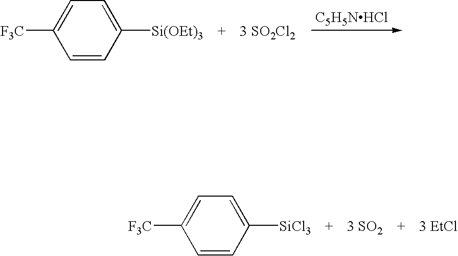
50.22 g (0.163 mol) 4-(trifluoromethyl)phenyl triethoxysilane, 83 mL (1.140 mol, 135.62 g) thionylchloride and 2.45 g (0.021 mol) pyridinium hydrochloride were refluxed and stirred for 16 h. Excess of SOCl2 was evaporated and residue was fractionally distilled to obtain 37 g (81%) 4-(trifluoromethyl)phenyl trichlorosilane. B.p. 44° C./4.0 mbar.
Characterization:
-
- 29Si: −63.0 ppm
- 13C: 139.3 ppm (C1) 137.4 ppm (C2,6) 126.4 ppm (C3,5) 134.4 ppm (qu, C4), 2JC4-F 31.7 Hz 126.6 ppm (qu, C7), 1JC7-F 271.4 Hz 60.8 ppm (C8) 20.0 ppm (C9)
-
- 29Si: −1.5 ppm
- 13C: 138.1 ppm (C1) 136.0 ppm (C2,6) 127.7 ppm (C3,5) 137.0 ppm (qu, C4), 2JC4-F 33.3 Hz 125.9 ppm (qu, C7), 1JC7-F 272.2 Hz
- 19F: −65.3 ppm

125.11 g (0.427 mol) 3,5-bis(trifluoromethyl)phenyl bromide, 10.38 g (0.427 mol) magnesium, and a small amount of iodine are stirred for half an hour. 356.78 g (382 ml, 1.708 mol) Si(OEt)4 is added to solution. Et2O is added until exothermic reaction occurs (˜200 ml) and the solution is refluxed for over night. Et2O is evaporated off and 250 ml n-heptane is added. Mg-salts are filtered off. n-heptane is evaporated and remaining 3,5-(F3C)2C6H3Si(OEt)3 is purified by distillation. B.p. 80° C./0.8 mbar. Yield 78.72 g (52%).

61.35 g (0.163 mol) 3,5-bis(trifluoromethyl)phenyl triethoxysilane, 83 mL (1.140 mol, 135.62 g) thionylchloride and 2.45 g (0.021 mol) pyridinium hydrochloride were refluxed and stirred for 16 h. Excess of SOCl2 was evaporated and residue was fractionally distilled to obtain 44.2 g (78%) 3,5-bis(trifluoromethyl)phenyl trichlorosilane. B.p. 41° C./3.1 mbar.

106.29 g (0.407 mol) pentafluorophenylmethyl bromide, 1.20 g (0.004 mol) Bu4PCl, and 187.55 g (140 ml, 1.385 mol) HSiCl3 were added to high pressure vessel. Solution was heated to 150° C. for four hours. Excess HSiCl3 was evaporated and C6F5CH2SiCl3 was purified by distillation. B.p. 56° C./2.4 mbar. Yield 91.18 g (71%).
| (#4) |  | Pentafluorophenyl ethyl trichlorosilane |
| (#5) | | Norbornyl trichlorosilane |
| (#6) |  | Pentafluoronorbornyl trichlorosilane |
| (#7) |  | 3,4,5-trimethylphenyl trichlorosilane |
| (#8) |  | 3-trifluoromethyl-4- (methyl)phenyl trichlorosilane |
| (#9) |  | 5-trifluoromethyl cyclooctatetraene- trichlorosilane |
| (#10) |  | 4-trifluoromethyl tetrafluorophenyl methyl trichlorosilane |
All above-mentioned monomers can be applied in organosilanol, organoalkoxysilane and organochlorosilane forms or in their combinations. In addition the number of organic functionalities in the above-mentioned precursors may vary from 1-3 also in such away that the organic functionalities are different from each other.
Formation of Dielectric Film Via the CVD Process
Claims (5)
Priority Applications (1)
| Application Number | Priority Date | Filing Date | Title |
|---|---|---|---|
| US10/563,801 US7646081B2 (en) | 2003-07-08 | 2004-07-08 | Low-K dielectric material |
Applications Claiming Priority (4)
| Application Number | Priority Date | Filing Date | Title |
|---|---|---|---|
| US48511403P | 2003-07-08 | 2003-07-08 | |
| US53167203P | 2003-12-23 | 2003-12-23 | |
| US10/563,801 US7646081B2 (en) | 2003-07-08 | 2004-07-08 | Low-K dielectric material |
| PCT/FI2004/000440 WO2005004221A2 (en) | 2003-07-08 | 2004-07-08 | Low-k-dielectric material |
Publications (2)
| Publication Number | Publication Date |
|---|---|
| US20070190800A1 US20070190800A1 (en) | 2007-08-16 |
| US7646081B2 true US7646081B2 (en) | 2010-01-12 |
Family
ID=33567748
Family Applications (1)
| Application Number | Title | Priority Date | Filing Date |
|---|---|---|---|
| US10/563,801 Expired - Lifetime US7646081B2 (en) | 2003-07-08 | 2004-07-08 | Low-K dielectric material |
Country Status (2)
| Country | Link |
|---|---|
| US (1) | US7646081B2 (en) |
| WO (1) | WO2005004221A2 (en) |
Families Citing this family (8)
| Publication number | Priority date | Publication date | Assignee | Title |
|---|---|---|---|---|
| US7915735B2 (en) | 2005-08-05 | 2011-03-29 | Micron Technology, Inc. | Selective metal deposition over dielectric layers |
| JP4935111B2 (en) * | 2006-02-22 | 2012-05-23 | 富士通株式会社 | Composition for forming insulating film, insulating film for semiconductor device, method for producing the same, and semiconductor device |
| CN100527367C (en) * | 2006-08-31 | 2009-08-12 | 联华电子股份有限公司 | Stack structure and method of patterning with this stack structure |
| KR102106885B1 (en) * | 2013-03-15 | 2020-05-06 | 삼성전자 주식회사 | Precursors for deposition of silicon dioxide film, and method for fabricating semiconductor device using the same |
| US9093265B2 (en) * | 2013-10-15 | 2015-07-28 | Taiwan Semiconductor Manufacturing Co., Ltd. | High UV curing efficiency for low-k dielectrics |
| KR102546316B1 (en) * | 2016-08-09 | 2023-06-21 | 삼성전자주식회사 | Semiconductor device including metal-semiconductor junction |
| CN110158052B (en) | 2019-05-17 | 2021-05-14 | 江苏菲沃泰纳米科技股份有限公司 | Low dielectric constant film and preparation method thereof |
| CN110129769B (en) | 2019-05-17 | 2021-05-14 | 江苏菲沃泰纳米科技股份有限公司 | Hydrophobic low dielectric constant film and method for preparing same |
Citations (6)
| Publication number | Priority date | Publication date | Assignee | Title |
|---|---|---|---|---|
| EP0713927A1 (en) | 1994-11-28 | 1996-05-29 | Air Products And Chemicals, Inc. | Fluorine doped silicon oxide coating process |
| US20020004298A1 (en) | 1996-08-29 | 2002-01-10 | Matsushita Electric Industrial Co., Ltd. | Method of forming interlayer insulating film |
| US20020076944A1 (en) | 2000-11-09 | 2002-06-20 | Wang Qing Min | Organosilane CVD precursors and their use for making organosilane polymer low-k dielectric film |
| US20040038514A1 (en) * | 1998-02-05 | 2004-02-26 | Asm Japan K.K. | Method for forming low-k hard film |
| WO2004027110A2 (en) | 2002-09-18 | 2004-04-01 | Arch Specialty Chemicals, Inc. | Additives to prevent degradation of alkyl-hydrogen siloxanes |
| US20050130404A1 (en) * | 2002-05-08 | 2005-06-16 | Applied Materials, Inc. | Methods and apparatus for e-beam treatment used to fabricate integrated circuit devices |
-
2004
- 2004-07-08 WO PCT/FI2004/000440 patent/WO2005004221A2/en not_active Ceased
- 2004-07-08 US US10/563,801 patent/US7646081B2/en not_active Expired - Lifetime
Patent Citations (6)
| Publication number | Priority date | Publication date | Assignee | Title |
|---|---|---|---|---|
| EP0713927A1 (en) | 1994-11-28 | 1996-05-29 | Air Products And Chemicals, Inc. | Fluorine doped silicon oxide coating process |
| US20020004298A1 (en) | 1996-08-29 | 2002-01-10 | Matsushita Electric Industrial Co., Ltd. | Method of forming interlayer insulating film |
| US20040038514A1 (en) * | 1998-02-05 | 2004-02-26 | Asm Japan K.K. | Method for forming low-k hard film |
| US20020076944A1 (en) | 2000-11-09 | 2002-06-20 | Wang Qing Min | Organosilane CVD precursors and their use for making organosilane polymer low-k dielectric film |
| US20050130404A1 (en) * | 2002-05-08 | 2005-06-16 | Applied Materials, Inc. | Methods and apparatus for e-beam treatment used to fabricate integrated circuit devices |
| WO2004027110A2 (en) | 2002-09-18 | 2004-04-01 | Arch Specialty Chemicals, Inc. | Additives to prevent degradation of alkyl-hydrogen siloxanes |
Non-Patent Citations (1)
| Title |
|---|
| Saito, N. et al., "Surface potential images of self-assembled monolayers patterned by organosiloxanes: ab initio molecular orbital calculations", Surface and Interface Analysis, 2002, 34, pp. 601-605. |
Also Published As
| Publication number | Publication date |
|---|---|
| WO2005004221A2 (en) | 2005-01-13 |
| WO2005004221A3 (en) | 2005-06-02 |
| US20070190800A1 (en) | 2007-08-16 |
Similar Documents
| Publication | Publication Date | Title |
|---|---|---|
| US7622399B2 (en) | Method of forming low-k dielectrics using a rapid curing process | |
| KR100907387B1 (en) | Curing dielectric films under a reducing atmosphere | |
| US6974970B2 (en) | Semiconductor device | |
| TW476705B (en) | Low k dielectric inorganic/organic hybrid film and method of making | |
| US7915180B2 (en) | SiCOH film preparation using precursors with built-in porogen functionality | |
| KR100984195B1 (en) | Active chemical process to enhance the properties of dielectric films | |
| KR100618304B1 (en) | Coating liquid and substrate coated with the film for forming silica-comprising film having low dielectric constant | |
| US20090278254A1 (en) | Dielectric materials and methods for integrated circuit applications | |
| CN1367205A (en) | Organosilicon precursors for low dielectric constant interlayer dielectric films | |
| JP2008074963A (en) | Composition, membrane, and method for producing the same | |
| US20080274627A1 (en) | Silicon-containing film, forming material, making method, and semiconductor device | |
| WO2003059990A1 (en) | Thin films and methods for the preparation thereof | |
| KR20090127140A (en) | High Silicon Silicon Polymers for Integrated Circuits | |
| JPH10284486A (en) | Method of forming interlayer insulating film | |
| US7646081B2 (en) | Low-K dielectric material | |
| JP7637129B2 (en) | Monoalkoxysilanes and dialkoxysilanes and dense organosilica films made therefrom | |
| TWI822044B (en) | Composition for vapor deposition of dielectric film and method for depositing organosilica film | |
| JP2006156539A (en) | Plasma reaction gas | |
| US20050136687A1 (en) | Porous silica dielectric having improved etch selectivity towards inorganic anti-reflective coating materials for integrated circuit applications, and methods of manufacture | |
| US20060180900A1 (en) | Organo-silsesquioxane polymers for forming low-k dielectrics | |
| TWI772883B (en) | Monoalkoxysilanes and dense organosilica films made therefrom | |
| JP5251156B2 (en) | Silicon-containing film and method for forming the same | |
| US20070063188A1 (en) | Low-k dielectric material | |
| CN110952074B (en) | Silicon compound and method of depositing film using silicon compound | |
| TW202217051A (en) | Alkoxydisiloxanes and dense organosilica films made therefrom |
Legal Events
| Date | Code | Title | Description |
|---|---|---|---|
| AS | Assignment |
Owner name: SILECS OY, FINLAND Free format text: ASSIGNMENT OF ASSIGNORS INTEREST;ASSIGNOR:RANTALA, JUHA;REEL/FRAME:019033/0010 Effective date: 20060830 |
|
| FEPP | Fee payment procedure |
Free format text: PETITION RELATED TO MAINTENANCE FEES GRANTED (ORIGINAL EVENT CODE: PTGR); ENTITY STATUS OF PATENT OWNER: SMALL ENTITY |
|
| STCF | Information on status: patent grant |
Free format text: PATENTED CASE |
|
| FEPP | Fee payment procedure |
Free format text: PAYOR NUMBER ASSIGNED (ORIGINAL EVENT CODE: ASPN); ENTITY STATUS OF PATENT OWNER: SMALL ENTITY |
|
| FPAY | Fee payment |
Year of fee payment: 4 |
|
| FPAY | Fee payment |
Year of fee payment: 8 |
|
| MAFP | Maintenance fee payment |
Free format text: PAYMENT OF MAINTENANCE FEE, 12TH YR, SMALL ENTITY (ORIGINAL EVENT CODE: M2553); ENTITY STATUS OF PATENT OWNER: SMALL ENTITY Year of fee payment: 12 |