US7645618B2 - Dry etch stop process for eliminating electrical shorting in MRAM device structures - Google Patents
Dry etch stop process for eliminating electrical shorting in MRAM device structures Download PDFInfo
- Publication number
- US7645618B2 US7645618B2 US11/724,556 US72455607A US7645618B2 US 7645618 B2 US7645618 B2 US 7645618B2 US 72455607 A US72455607 A US 72455607A US 7645618 B2 US7645618 B2 US 7645618B2
- Authority
- US
- United States
- Prior art keywords
- insulating layer
- oxygen
- metal layer
- reactive gas
- substrate
- Prior art date
- Legal status (The legal status is an assumption and is not a legal conclusion. Google has not performed a legal analysis and makes no representation as to the accuracy of the status listed.)
- Expired - Lifetime, expires
Links
Images


Classifications
-
- H—ELECTRICITY
- H10—SEMICONDUCTOR DEVICES; ELECTRIC SOLID-STATE DEVICES NOT OTHERWISE PROVIDED FOR
- H10N—ELECTRIC SOLID-STATE DEVICES NOT OTHERWISE PROVIDED FOR
- H10N50/00—Galvanomagnetic devices
- H10N50/01—Manufacture or treatment
Definitions
- the present invention relates generally to semiconductor fabrication and particularly to fabricating device structures containing metal-insulator-metal layered thin film stacks such as those used in magnetic tunnel junction devices and memory devices.
- Layered films of metal-insulator-metal are employed as storage elements in memory devices such as magnetic random access memories (MRAM) and the like.
- the memory element for the MRAM technology is a patterned structure of multilayer material and is usually composed of a stack of different materials such as NiFe, CoFe, PtMn, Ru, etc., and may include insulator-like materials such as Al 2 O 3 or MgO.
- a typical stack may contain as many as ten or more layers of these materials some of which are non-magnetic, some of which are magnetic, and one or two of which are insulating.
- the insulating films in this description are defined as oxidized or nitridized metal layers that exhibit high electrical resistance in their bulk form. To fabricate a storage element, it is necessary to deposit the materials in overlying blanket films, layer by layer, to form a patterned layer of photoresist, and to etch the films into appropriate structures.
- Ion beam milling or ion beam etching processes have been employed to remove magnetoresistive materials.
- Ion beam milling is a physical milling process. Areas that are not protected by the mask are removed by bombardment with ions. The bombardment of ions sputters or peels away the unprotected material. Ion beam milling operates with low selectivity, and the portions of the stack that are near to the edges of the mask or the boundaries of an MRAM cell body can be easily damaged.
- etching techniques have also been employed to selectively remove portions of deposited layers. Examples of etching techniques include dry etching techniques and wet etching techniques.
- One of the drawbacks of current etching techniques is that the profiles of MRAM structures are susceptible to electrical shorting across the thin tunnel junction.
- the vertical separation between the upper magnet layer above the insulating dielectric tunneling layer and the lower magnet layer below this tunneling layer is inadequate to prevent electrical shorting.
- Embodiments of the present invention are directed to, among other things, fabrication of magnetic tunnel junction (MTJ) devices whereby the tunnel barrier layer serves as the stop layer during plasma overetching of the upper magnetic layer.
- MTJ magnetic tunnel junction
- the gases employed during plasma overetching preferably excludes halogen containing species which result in highly selective etching of the upper magnetic layer vis-à-vis the tunnel barrier layer.
- the introduction of oxygen in the gas enhances the reproducibility of the process.
- a fluorine-chlorine gas mixture is employed to partially etch the magnet layer over the tunnel barrier layer.
- another embodiment is directed to corrosion plasma treatment with He and H 2 gas prior to or during the stripping of the photoresist mask.
- rinsing with water and He and H 2 dehydration baking can be employed following the stripping step.
- FIG. 1 Typical MRAM structure with magnetic tunneling junction.
- FIG. 2 Simplified MRAM structure with magnetic tunneling junction
- FIG. 3 Inventive MRAM process sequence
- FIG. 4 Inventive MRAM process sequence
- FIG. 5 a Inventive MRAM process sequence
- FIG. 5 b Inventive MRAM process sequence
- FIG. 6 MRAM stack structure after top contact patterning
- FIG. 7 MRAM stack structure after reactive magnet-layer etch step
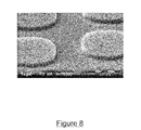
- FIG. 8 MRAM stack structure after reactive magnet-layer etch
- FIG. 9 Embodiment of the inventive MRAM patterning sequence in which the tunneling dielectric layer is not breached in the vicinity of the feature but is breached in areas not in close proximity to the mask feature
- FIG. 10 Embodiment of the inventive MRAM patterning sequence in which the magnetic stack layers are intentionally etched with a sloped profile during a reactive etch step prior to the etch stop process
- FIG. 11 Plot of optical emission signal intensity obtained during the etch of a 50 ⁇ NiFe/15 ⁇ alumina/50 ⁇ NiFe stack structure.
- the two peaks in the plot indicate the removal of the two NiFe layers.
- the time between the two peaks indicate the time required to remove the 15 ⁇ alumina layer.
- the NiFe-to-alumina etch selectivity obtained from the process used to produce the graph is greater than 90:1.
- FIG. 12 Graph of etch sputter rates for CoFe, NiFe, and alumina.
- FIG. 13 MRAM stack structure after reactive magnet layer etch (see FIG. 6 ) and etch stop process
- FIG. 14 MRAM stack structure after reactive magnet layer etch (see FIG. 7 ) and etch stop process
- FIG. 15 MRAM stack structure after reactive magnet layer etch (see FIG. 8 ) and etch stop process
- the present invention is based, in part, on the development of a patterning method for fabricating magnetic tunnel junction (MTJ) devices that are employed in magnetic random access memory (MRAM) devices.
- MTJ magnetic tunnel junction
- MRAM magnetic random access memory
- a critical aspect of the invention is that MTJ devices prepared by the inventive process afford superior electrical isolation between the magnet layers in contact with the dielectric tunnel layer in comparison to the current art.
- FIG. 1 A typical MRAM structure, within which an MTJ is contained, is shown in FIG. 1 .
- the MRAM structure is a complex stack of magnetic, conductive, and insulating films on a substrate.
- the specific components of a typical MRAM structure are shown and consist of a substrate 10 , a barrier layer 12 , a bottom contact layer 14 , a mulitlayer fixed magnet structure 16 consisting of layers of CoFe, Ru, NiFe, IrMn, PtMn, and the like, a dielectric tunnel layer such as alumina or MgO 18 , a switchable magnet layer 20 (NiFe, CoFe, CoNiFe, CoFeB, and the like), and a top contact layer 22 (Ta, TaN, Ti, TiN, W, and the like).
- Photoresist layer 28 is a light sensitive material that is commonly used by those skilled in the art of electrical device fabrication as a mask to etch one or more of the underlying layers below the photoresist so that portions of the underlying layer not protected by the resist layer can be etched away.
- Antireflection coating 26 which is typically 300 ⁇ to 800 ⁇ thick, is commonly used to absorb radiation to form an optically opaque film to enhance the contrast of the imaging resist. ARC coatings effectively reduce reflection of the incident radiation back into the overlying PR mask layer. This prevents overexposure of the photoresist material.
- Hard mask layer 24 is commonly used in device fabrication as an intermediate mask transfer layer.
- the photoresist is used as a dry etch mask to transfer the pattern into the hard mask, and possibly one or more of the underlayers, after which the hard mask layer is used as a mask to transfer the pattern into the remaining underlayers that are not defined using the photoresist.
- Hard masks such as silicon dioxide and silicon nitride are commonly used as a means to improve the durability of the mask relative to that of photoresist or to allow processing at temperatures above the softening point of polymeric photoresist layers.
- Magnetic stack structure are typically formed on a substrate 10 .
- the substrate 10 may include any structure that has an exposed surface. Structures are preferably those used in the manufacture of semiconductor devices such as silicon wafer, silicon-on insulator (SOI), silicon-on sapphire (SOS), aluminum titanium carbide (AlTiC) doped and undoped semiconductors, III-V or II-VI semiconductors, epitaxial layers of silicon supported by a base semiconductor foundation, and other semiconductor structures.
- the semiconductor need not be silicon-based.
- the semiconductor could be silicon-germanium, germanium, or gallium arsenide.
- the structure could also be a non-semiconductor such as glass or polymer.
- the substrate 10 may include buried electronic devices such as transistors, diodes, capacitors, and resistors, or any other device or circuit element that would be used in conjunction with the magnetic multilayer stack.
- MTJ multilayer MRAM structure
- MTJ and MRAM structures are known in the art and are described, for example, in U.S. Pat. No. 6,673,675 to Yates, et al., entitled “Methods of Fabricating an MRAM Device Using Chemical Mechanical Polishing”; U.S. Pat. No. 6,677,165 to Lu, et al., entitled “Magnetoresistive Random Access Memory (MRAM) Cell Patterning”; U.S. Pat. No.
- the orientation of the magnetic film stack can be reversed relative to the order shown in FIG. 1 . That is, the orientation of the film structure can be such that the film stack can be deposited in reverse order with the top contact layer and free magnet layer are below the dielectric tunnel layer and the multi-layer fixed and antiferromagnetic layers are placed above the dielectric tunnel layer. It should also be understood that the magnetic film stack can comprise multiple magnetic tunnel junctions in orientations in which the free layer is deposited above the dielectric tunnel layer or below the dielectric tunnel layer and remain within the scope of the inventive method.
- the MTJ stack comprises a substrate 10 , a bottom contact layer 14 , a fixed bottom magnet layer 16 , a dielectric tunnel layer 18 , a switchable upper magnet layer 20 , and a top contact layer 22 .
- the stack structure is patterned with photoresist layer 28 . This simplified structure is used in the following description of the preferred embodiments for the present invention.
- FIGS. 3 , 4 , and 5 Inventive etch-stop process sequences are provided in FIGS. 3 , 4 , and 5 .
- FIG. 3 shows an inventive process sequence in which the magnetic stack is deposited 100 , the PR is patterned 102 , one or both of the hard mask and top contact layers are etched 104 , and a reactive etch process is used to remove part of the upper magnet layer 106 .
- MTJ device structures are exposed to an inventive etch stop process 108 directly, or first to a corrosion treatment sequence consisting of a Dl rinse, a PR strip, and a plasma based corrosion treament, followed by an inventive etch stop process 108 .
- the inventive etch stop process 108 directly follows the reactive partial etch of the upper magnet 106
- the patterning of the MTJ device structures is completed and the devices are moved to subsequent processing 114 .
- the inventive etch stop process 108 directly follows the reactive partial etch of the upper magnet 106
- the devices are exposed to a sequence of processes to prevent corrosion. Exposure of magnetic films to chlorine- and bromine-containing etch chemistries can produce adverse reactions upon removal of the devices from vacuum and subsequent exposure of the etched films to moisture under ambient conditions. Depending on the sensitivity of the films, various sequences have been developed for preventing adverse corrosive reactions such as those shown in FIG. 3 .
- the corrosion treatment sequence consists of a Dl water rinse 110 followed by a photoresist strip/corrosion treatment 112 .
- the corrosion prevention treatment sequence consists of a photoresist strip/corrosion treatment 112 , followed by Dl water rinse 110 .
- the inventive etch stop process 108 does not directly follow the reactive partial etch of the upper magnet 106 , but rather is preceded by corrosion prevention treatments 110 and 112 .
- the MTJ device structures are exposed to a Dl water rinse 110 followed by a photoresist strip/corrosion treatment 112 prior to the inventive etch stop on the tunnel layer 108 .
- the devices are exposed to a photoresist strip/corrosion treatment 112 followed by a Dl water rinse prior to the inventive etch stop on the tunnel layer 108 .
- FIG. 4 shows an inventive process sequence in which the magnetic stack is deposited 100 , the PR is patterned 102 , and the hard mask is etched 103 . Following the hard mask etch 103 , MTJ device structures are exposed to a photoresist strip process 107 or to a reactive etch process 105 to remove the top contact layer and a reactive etch process 106 to remove part of the upper magnet. In a first embodiment of the inventive process in which the hard mask etch process 103 is followed by photoresist strip process 107 , subsequent to the photoresist process 107 the MTJ devices are exposed to a reactive etch process 105 to remove the top contact layer and a reactive etch process 106 to remove part of the upper magnet.
- the MTJ devices are subsequently exposed to a photoresist strip process 107 .
- the MTJ devices are exposed to the etch stop process 108 directly, or first to a corrosion treatment sequence consisting of a Dl rinse and a plasma based corrosion treament 113 , followed by an inventive etch stop process 108 .
- the inventive etch stop process 108 directly follows the reactive partial etch of the upper magnet 106 , or follows a photoresist strip process 107 that was preceded by the reactive partial etch of the upper magnet 106 , the patterning of the MTJ device structures is completed and the devices are moved to subsequent processing 114 .
- the inventive etch stop process 108 directly follows the reactive partial etch of the upper magnet 106 , or follows a photoresist strip process 107 that was preceded by the reactive partial etch of the upper magnet 106 , the devices are exposed to a sequence of processes to prevent corrosion.
- Exposure of magnetic films to chlorine- and bromine-containing etch chemistries can produce adverse reactions upon removal of the devices from vacuum and subsequent exposure of the etched films to moisture under ambient conditions.
- various sequences have been developed for preventing adverse corrosive reactions such as those shown in FIG. 4 .
- the corrosion prevention treatment sequence consists of a Dl water rinse 110 followed by a plasma-based corrosion treatment 112 .
- the corrosion prevention treatment sequence consists of a plasma-based corrosion prevention treatment 112 , followed by Dl water rinse 110 .
- the inventive etch stop process 108 does not directly follow the reactive partial etch of the upper magnet 106 , but rather is preceded by corrosion prevention treatments 110 and 113 .
- the MTJ device structures are exposed to a Dl water rinse 110 followed by a plasma-based corrosion treatment 113 prior to the inventive etch stop on the tunnel layer 108 .
- the devices are exposed to a plasma-based corrosion treatment 113 followed by a DI water rinse prior to the inventive etch stop on the tunnel layer 108 .
- FIG. 5 a and FIG. 5 b Two approaches to the subsequent processing 114 , as indicated in FIG. 3 and FIG. 4 , are shown in FIG. 5 a and FIG. 5 b . These figures describe two specific methods that specifically exploit the unique capability afforded by inventive etch stop process step 108 .
- FIG. 5 a a spacer is used to passivate the sidewall of the MTJ device structure to prevent electrical shorting during subsequent processing.
- the sidewall spacer is used in conjunction with an etch stop process such as that described by etch stop process 108 shown in FIGS. 3 and 4 .
- FIG. 5 a shows the preferred embodiment for subsequent processing steps that follow the inventive etch stop process 108 shown in FIGS. 3 and 4 .
- 3 and 4 consist of a spacer dielectric deposition 130 , a spacer etch 132 , and a bottom magnet/bottom contact etch 134 to complete the process or a bottom magnet/bottom contact etch 134 followed by a Dl water rinse step followed by a plasma-based corrosion prevention treatment 142 .
- the plasma-based corrosion prevention treatment 142 can precede the Dl water rinse as shown in FIG. 5 a before proceeding with subsequent processing of the device 150 .
- FIG. 5 b an alternative approach to subsequent processing 114 is shown in which an insulating hard mask layer such as silicon dioxide or silicon nitride is deposited 120 , photoresist is patterned 122 , the hard mask is etched 124 , the photoresist is stripped 126 , and the bottom magnet and bottom contact are etched 128 .
- the photoresist patterning is such that the silicon dioxide or silicon nitride hard mask layer extends laterally beyond the vertical sidewall produced from the original hard mask etch 103 , upper contact etch 105 , reactive upper magnet etch 106 , and etch stop process 108 .
- the lateral extension of hard mask 120 beyond the vertical sidewall, upon photoresist patterning 122 , should be such that the sidewall of the original hardmask, the upper contact, and the upper magnet layer remains covered with hard mask layer 120 after hard mask layer etch 124 .
- the layers that comprise the MRAM stack or other magnetic device structure are deposited 100 using techniques employed by those skilled in the art of film deposition.
- the films may be deposited by physical vapor deposition, chemical vapor deposition, atomic layer deposition, nano-layer deposition, atomic layer deposition, evaporation, and other techniques.
- the films in the stack may also be deposited by one of these methods in one form and subsequently modified in a second chamber.
- the alumina (Al 2 O 3 ) dielectric for example, might be formed by depositing a layer of aluminum and subsequently exposing the aluminum to an oxidizing process to form alumina.
- MgO might be formed by depositing a layer of magnesium and subsequently exposing the Mg to an oxidizing process to form MgO.
- a photoresist deposition and patterning step 102 is used to create a pattern for defining the MTJ or MRAM stack.
- an antireflective coating can be used in conjunction with the photoresist to improve the accuracy of the pattern transfer.
- a hard mask layer can be incorporated between the photoresist and the top contact layer. Hard mask layers such as silicon dioxide and silicon nitride could be used. Alternatively, the thickness of the conductive top contact layer can be made such that it can serve the dual purpose of hard mask and top contact layer.
- FIG. 2 shows the simplified MRAM stack structure after magnetic stack deposition 100 and subsequent photoresist patterning 102 .
- the hard mask layer and the upper contact layer layers are patterned 103 using common techniques employed by those skilled in the art.
- One example of a common process for reactively etching a silicon oxide hard mask, if present, is to use a mixture of CF 4 , CHF 3 , and Ar.
- Oxide etch processes are widely available in the literature.
- an example of a process chemistry that is commonly used to reactively etch the top conductor layer 104 , 105 is the use a mixture of Ar/Cl 2 .
- metal contact layer etches have been published extensively in the literature. Oxide and nitride hard masks and metal contact layers have been in use for many years and the techniques that have been used to remove these layers are apparent to those skilled in the art.
- the simplified MRAM stack structure after contact etch is shown in FIG. 6 .
- This inventive process 106 consists of a gas mixture of a chlorine-containing gas such as Cl 2 , BCl 3 , and HCl and a fluorine-containing gas such as CF 4 , SF 6 , and CHF 3 to remove part of the top magnet layer.
- a gas molecule that contains Cl and F atoms might be used.
- the ratio of chlorine-containing to fluorine-containing gases should be in the range of 2:1 to 20:1.
- Typical process conditions for the reactive etch step 106 demonstrated in the Spectra® inductively coupled process module manufactured by Tegal Corporation, are as follows: 400 W of 13.56 MHz rf power on the inductive source coil, 20 W of 450 kHz rf power applied to the substrate, 40 sccm Cl 2 , 8 sccm CF 4 , and 4 mT process pressure.
- the simplified MRAM stack structure after reactive magnet layer etch 106 is shown in FIG. 7 .
- fluorine as an additive to a chlorine-containing etch process has been found to produce smooth etched surfaces (as shown in FIG. 8 ) and prevent diffusion of the chlorine species through very thin films of magnetic material that remain after reactive upper magnet etch step 106 .
- Use of a fluorine/chlorine containing gas mixture allows for removal of the upper magnet layer to within 5-25 ⁇ of the interface between the remaining upper magnet layer and the underlying dielectric tunnel layer.
- the remaining upper magnet layer will be etched as close as possible to the interface between the remaining upper magnet layer 20 and the underlying dielectric layer 18 without penetrating the tunneling dielectric layer in the vicinity of the features prior to moving to a subsequent processing step such as the etch stop process 108 , the Dl water rinse 110 , or the PR strip/corrosion treatment 112 .
- the upper magnet layer 20 is etched uniformly and the underlying dielectric layer 18 is not breached anywhere on the wafer during the reactive upper magnet layer etch 106 as shown in FIG. 7 .
- the upper magnet layer 20 is completely removed and the underlying dielectric layer 18 is breached, but not within close proximity of the patterned MTJ stack features (See FIG. 9 ).
- the upper magnet layer etch 106 is removed with an etch process that contains one or more of the following gases or gas mixtures: Cl 2 , Cl 2 /Ar, Cl 2 /CF 4 , Cl 2/ CHF 3 , Cl 2/ Ar, BCl 3 /Cl 2 , BCl 3/ Cl 2/ Ar, BCl 3/ HBr,/Ar, BCl 3/ HBr/Ar,NH 3 , NH 3 /CO.
- the upper magnet layer 20 is completely removed, the underlying dielectric layer 18 is also removed outside of a sloped region in close proximity of the patterned MTJ stack, and all or part of the bottom magnet layer 16 and all or part of the bottom contact layer 14 are removed. (See FIG. 10 .)
- a unique benefit of this embodiment is that the full MRAM structure is patterned with a single mask; subsequent processing steps 114 are not required.
- the upper magnet layer etch 106 is removed with an etch process that contains one or more of the following reactive gases and gas mixtures: Cl 2 , Cl 2/ Ar, Cl 2 /CF 4 , Cl 2 /CHF 3 , Cl 2 /Ar, BCl 3 /Cl 2 , BCl 3 /Cl 2 /Ar, BCl 3 /HBr, BCl 3 /HBr/Ar, NH 3 , NH 3 /CO.
- etch stop process 108 consisting, in the preferred embodiment, of a mixture of a non-reactive gas such as argon and an oxidizing gas, such as oxygen, whereby the dielectric of the tunnel barrier layer serves as the stop layer.
- a non-reactive gas such as argon
- an oxidizing gas such as oxygen
- the inert gas flow is typically in the range of 10 to 350 sccm and the flow of the oxygen-containing gas is in the range of 0.02 to 0.15 sccm.
- Actual flows for the oxygen-containing gas can vary depending on the flow of inert gas, the selection of the oxygen-containing gas, and the type of plasma system used.
- a typical process 108 used in the Spectra® inductively coupled etch process module manufactured by Tegal Corporation is as follows for a 200 mm diameter silicon substrate: 100 W of 13.56 MHz rf power on the source coil, 20 W of 450 kHz rf power applied to the substrate, 350 sccm Ar, 0.08 sccm O 2 , and 10 mT process pressure.
- the conditions provided above for the etch stop, sputter process step 108 are intended to provide an exemplary set of conditions that have been found to produce a sputter selectivity between NiFe and alumina of ⁇ 90:1 in the Spectra lCP process module manufactured by Tegal Corporation. (See FIG. 11 .)
- a range of process conditions and chamber configurations can be used to produce results with high selectivity between the upper magnet material and the dielectric.
- Two factors that must be considered in achieving high selectivity are the control of the ratio of inert gas to oxygen-containing gas in the process chamber and the operation of the process at low bias power levels. These two factors are discussed in more detail in the following paragraphs.
- the etch stop process requires a high selectivity (>5:1) between the upper magnet layer 20 and the underlying dielectric layer 18 . It is expected that the upper magnet layer 20 will be etched at a rate of at least 5 times faster than the rate at which the underlying dielectric layer 18 , e.g., Al 2 O 3 , is etched. Precise control of the NiFe/CoFe etch rate is possible because there are significant differences in sputter thresholds between the NiFe and CoFe and that of oxidized metals such as Al 2 O 3 and MgO. Experiments that confirmed these phenomena were conducted using a Spectra® process module manufactured by Tegal Corporation (Petaluma, Calif).
- NiFe and CoFe sputter rates were measured with monolayer test wafers and alumina etch rates were measured with alumina/NiFe test structures.
- the test structure consisted of a substrate that had a NiFe layer deposited thereon and a very thin layer of alumina ( ⁇ 15 ⁇ ) over the NiFe.
- the measured alumina etch rates were representative of the thin film properties that would be found in stacks containing magnetic tunneling junctions.
- FIGS. 13 , 14 , and 15 The resulting device profiles following the preferred embodiments of reactive etch steps 106 as shown in FIGS. 7 , 9 , and 10 and etch stop process 108 are shown in FIGS. 13 , 14 , and 15 .
- the residual metal film that remains of upper magnet layer 20 after reactive etch step 106 is removed from the underlying dielectric layer 18 .
- the removal of the upper magnet layer 20 that remains after reactive step 106 with a low bias non-reactive etch stop 108 provides superior electrical isolation over other known methods without damaging the underlying dielectric layer 18 .
- Geometric isolation is provided in each of the three embodiments of the inventive process without the inherent risk of electrical shorting that has been known to limit device performance for structures incorporating MTJ stacks.
- Superior electrical isolation between the upper magnet layer 20 and the bottom magnet layer 16 is also accomplished with the inventive process without the associated risks involved in using corrosive chemistries at the stage of the process that is most critical for producing reliable devices.
- etch stop 108 The typical process conditions for etch stop 108 provided above are intended to be representative of a process that was found to yield an exceptionally high selectivity between NiFe or CoFe and alumina. Variations of the process conditions within the Spectra reactor can be used within the scope of the inventive etch stop process 108 .
- oxygen-containing gas can be eliminated by controlling the oxygen level in the etch chamber by a method other than the intentional introduction of an oxygen-containing gas as is discussed in the following paragraphs
- plasma sputtering magnetic layers comprising transition metals such as NiFe with inert sputtering gases such as Ar, that regulating the amount of oxygen in the plasma chamber can influence the etch selectivity with respect to the underlying alumina. That is, a higher NiFe/alumina selectivity can be achieved by controlling the flow of oxygen into the plasma chamber.
- One embodiment of the plasma overetch process entails reducing the background oxygen to levels that do not affect the etching process while concurrently re-introducing oxygen in a measurable and controllable manner into the plasma chamber.
- Sources of the background oxygen that may enter the plasma chamber include, for example: (1) sputtering of oxygen-containing internal chamber parts, (2) atmospheric oxygen; (3) outgassing from materials in the chamber; and (4) other processing modules in the process system.
- the selectivity between NiFe and alumina can be optimized by re-introducing a very small amount (e.g., ⁇ 0.08 sccm) of oxygen into the chamber.
- a very small amount e.g., ⁇ 0.08 sccm
- One technique to re-introduce the oxygen employs two separate carrier gas sources that are connected to the chamber. The first source supplies an Ar/O 2 gas mixture comprising 99.9% Ar and 0.1% O 2 to the plasma chamber while a second source supplies a gas containing 100% Ar in parallel to the chamber.
- the base pressure of the chamber be reduced to ⁇ 0.001 mT or less. Additionally, the sputtering of the surfaces of internal chamber parts should be minimized or controlled.
- inductive source power should be low (100-200 W) to minimize window sputtering.
- Excessive amounts of oxygen in the chamber can slow the etch rate of the metallic magnetic films and can lead to a reduction in selectivity between the magnet layers and the dielectric layers.
- oxygen is introduced into the process chamber through an orifice separating a source of oxygen and the process chamber.
- the orifice is sized such that the flow of the oxygen containing gas, when mixed with an inert gas, produces an enhancement in the sputtering selectivity between the upper magnetic film and the tunneling dielectric.
- an inert gas such as argon would be introduced through conventional means, such as a mass flow controller or needle valve, at such a volume so as to produce a mixture of inert gas and oxygen-containing species at the surface of the upper magnetic layer being etched, so as to produce selective removal between the magnetic material and the tunneling dielectric layer.
- the process conditions would be adjusted such that the magnetic material would be removed at a rate of >5 ⁇ /min and the dielectric layer would be removed at a rate of ⁇ 1 ⁇ /min.
- the level of an oxygen-containing gas is provided by controlling the leakage of atmospheric gases into the vacuum chamber.
- Plasma-based semiconductor fabrication processes are typically performed in the range of 0.1 to 1000 milliTorr.
- oxygen can be introduced inadvertently through imperfect seals, through porous materials, and from outgassing of parts in the processing chamber.
- the rate of leakage can easily be measured in conventional plasma processing equipment.
- an inert gas such as argon would be introduced through conventional means, such as a mass flow controller or needle valve, at such a volume so as to produce a mixture of inert gas and oxygen-containing species at the surface of the upper magnetic layer being etched, so as to produce selective removal between the magnetic material and the tunneling dielectric layer.
- conventional means such as a mass flow controller or needle valve
- oxygen-containing species such as argon
- the approach of controlling the oxygen-containing leakage from atmosphere in combination with the introduction of controlled inert gas flow through conventional means to produce the required mixture of inert gas and oxygen-containing species to the extent that the magnetic material is removed at a rate of >5 ⁇ /min and the dielectric layer is removed at a rate of ⁇ 1 ⁇ /min.
- the process for removing the photoresist and preventing corrosion must be compatible with magnetic film structures.
- the use of hydrogen-containing gas mixtures that are suitable for resist removal and for preventing corrosion that could result from exposure of the MRAM film stack to the halogen-containing etch chemistries.
- the magnetic film stack is exposed to a hydrogen-containing plasma to remove the photoresist, to expose the magnetic layers to a process that would prevent corrosion upon exposure to ambient conditions, or both.
- Hydrogen is introduced into the process chamber in a mixture of hydrogen and an inert gas such as helium, neon, argon, or nitrogen.
Landscapes
- Engineering & Computer Science (AREA)
- Manufacturing & Machinery (AREA)
- Hall/Mr Elements (AREA)
- Mram Or Spin Memory Techniques (AREA)
Abstract
Description
Claims (64)
Priority Applications (6)
| Application Number | Priority Date | Filing Date | Title |
|---|---|---|---|
| US11/724,556 US7645618B2 (en) | 2004-09-09 | 2007-03-14 | Dry etch stop process for eliminating electrical shorting in MRAM device structures |
| PCT/US2007/006607 WO2007109117A2 (en) | 2006-03-16 | 2007-03-16 | Dry etch stop process for eliminating electrical shorting in mram device structures |
| JP2009500499A JP5085637B2 (en) | 2006-03-16 | 2007-03-16 | Dry etch stop process to eliminate electrical shorts in MRAM device structure |
| KR1020087025349A KR20090008240A (en) | 2006-03-16 | 2007-03-16 | Dry etch stop method for removing electrical shorts in MRM device structures |
| EP07753250A EP1999781A2 (en) | 2006-03-16 | 2007-03-16 | Dry etch stop process for eliminating electrical shorting in mram device structures |
| US12/552,664 US7955870B2 (en) | 2006-03-16 | 2009-09-02 | Dry etch stop process for eliminating electrical shorting in MRAM device structures |
Applications Claiming Priority (3)
| Application Number | Priority Date | Filing Date | Title |
|---|---|---|---|
| US10/937,660 US7169623B2 (en) | 2004-09-09 | 2004-09-09 | System and method for processing a wafer including stop-on-aluminum processing |
| US78317506P | 2006-03-16 | 2006-03-16 | |
| US11/724,556 US7645618B2 (en) | 2004-09-09 | 2007-03-14 | Dry etch stop process for eliminating electrical shorting in MRAM device structures |
Related Parent Applications (1)
| Application Number | Title | Priority Date | Filing Date |
|---|---|---|---|
| US10/937,660 Continuation-In-Part US7169623B2 (en) | 2004-09-09 | 2004-09-09 | System and method for processing a wafer including stop-on-aluminum processing |
Related Child Applications (1)
| Application Number | Title | Priority Date | Filing Date |
|---|---|---|---|
| US12/552,664 Continuation US7955870B2 (en) | 2006-03-16 | 2009-09-02 | Dry etch stop process for eliminating electrical shorting in MRAM device structures |
Publications (2)
| Publication Number | Publication Date |
|---|---|
| US20070155027A1 US20070155027A1 (en) | 2007-07-05 |
| US7645618B2 true US7645618B2 (en) | 2010-01-12 |
Family
ID=38224947
Family Applications (1)
| Application Number | Title | Priority Date | Filing Date |
|---|---|---|---|
| US11/724,556 Expired - Lifetime US7645618B2 (en) | 2004-09-09 | 2007-03-14 | Dry etch stop process for eliminating electrical shorting in MRAM device structures |
Country Status (1)
| Country | Link |
|---|---|
| US (1) | US7645618B2 (en) |
Cited By (12)
| Publication number | Priority date | Publication date | Assignee | Title |
|---|---|---|---|---|
| US20110235217A1 (en) * | 2010-03-29 | 2011-09-29 | Qualcomm Incorporated | Fabricating A Magnetic Tunnel Junction Storage Element |
| US20130034917A1 (en) * | 2011-08-04 | 2013-02-07 | Min Suk Lee | Method for fabricating magnetic tunnel junction device |
| US8546263B2 (en) * | 2011-04-27 | 2013-10-01 | Applied Materials, Inc. | Method of patterning of magnetic tunnel junctions |
| US8615868B2 (en) | 2011-11-29 | 2013-12-31 | HGST Netherlands B.V. | Method for manufacturing a magnetic sensor using two step ion milling |
| US20150255507A1 (en) * | 2014-03-07 | 2015-09-10 | Applied Materials, Inc. | Method of forming magnetic tunneling junctions |
| US20160079519A1 (en) * | 2014-09-11 | 2016-03-17 | Masatoshi Yoshikawa | Magnetic memory device and method of manufacturing magnetic memory device |
| US9472753B1 (en) | 2015-06-02 | 2016-10-18 | HGST Netherlands B.V. | Method for fabricating MRAM bits on a tight pitch |
| US20170062699A1 (en) * | 2015-08-31 | 2017-03-02 | Taiwan Semiconductor Manufacturing Company, Ltd. | Magnetoresistive Random Access Memory Cell and Fabricating the Same |
| US9705071B2 (en) | 2015-11-24 | 2017-07-11 | International Business Machines Corporation | Structure and method to reduce shorting and process degradation in STT-MRAM devices |
| US10475496B1 (en) | 2018-05-04 | 2019-11-12 | International Business Machines Corporation | Reduced shorts in magnetic tunnel junctions |
| US11121311B2 (en) | 2019-01-24 | 2021-09-14 | International Business Machines Corporation | MTJ containing device encapsulation to prevent shorting |
| DE102019113486B4 (en) | 2018-10-25 | 2021-12-02 | Taiwan Semiconductor Manufacturing Co., Ltd. | NEW HARD MASK FOR MTJ STRUCTURING |
Families Citing this family (13)
| Publication number | Priority date | Publication date | Assignee | Title |
|---|---|---|---|---|
| KR100831254B1 (en) * | 2006-11-27 | 2008-05-22 | 동부일렉트로닉스 주식회사 | MI of semiconductor device and forming method thereof |
| US8133745B2 (en) * | 2007-10-17 | 2012-03-13 | Magic Technologies, Inc. | Method of magnetic tunneling layer processes for spin-transfer torque MRAM |
| US8373948B2 (en) * | 2008-04-28 | 2013-02-12 | Hitachi Global Storage Technologies Netherlands B.V. | Tunnel magnetoresistance (TMR) structures with MGO barrier and methods of making same |
| SG157992A1 (en) * | 2008-07-01 | 2010-01-29 | Showa Denko Hd Singapore Pte L | Improvements in and relating to mram |
| US8482966B2 (en) * | 2008-09-24 | 2013-07-09 | Qualcomm Incorporated | Magnetic element utilizing protective sidewall passivation |
| KR101527533B1 (en) * | 2009-01-09 | 2015-06-10 | 삼성전자주식회사 | Method of forming magnetic memory device |
| US7863060B2 (en) * | 2009-03-23 | 2011-01-04 | Magic Technologies, Inc. | Method of double patterning and etching magnetic tunnel junction structures for spin-transfer torque MRAM devices |
| US20110007423A1 (en) * | 2009-07-13 | 2011-01-13 | Seagate Technology Llc | Supplemental Layer to Reduce Damage from Recording Head to Recording Media Contact |
| US8536063B2 (en) * | 2011-08-30 | 2013-09-17 | Avalanche Technology Inc. | MRAM etching processes |
| US9166154B2 (en) | 2012-12-07 | 2015-10-20 | Avalance Technology, Inc. | MTJ stack and bottom electrode patterning process with ion beam etching using a single mask |
| JP6347695B2 (en) * | 2013-11-20 | 2018-06-27 | 東京エレクトロン株式会社 | Method for etching a layer to be etched |
| US9576894B2 (en) * | 2015-06-03 | 2017-02-21 | GlobalFoundries, Inc. | Integrated circuits including organic interlayer dielectric layers and methods for fabricating the same |
| US12080561B2 (en) * | 2022-01-26 | 2024-09-03 | Nanya Technology Corporation | Method of processing substrate |
Citations (17)
| Publication number | Priority date | Publication date | Assignee | Title |
|---|---|---|---|---|
| US3811579A (en) | 1972-09-25 | 1974-05-21 | D Black | Mechanized van loading and unloading apparatus and system |
| US5538905A (en) * | 1992-10-21 | 1996-07-23 | Sharp Kabushiki Kaisha | Method for forming a transparent conductive ITO film |
| US5901758A (en) * | 1997-04-30 | 1999-05-11 | The Boc Group, Inc. | Method of filling gas containers |
| US5980686A (en) | 1998-04-15 | 1999-11-09 | Applied Komatsu Technology, Inc. | System and method for gas distribution in a dry etch process |
| US6114719A (en) | 1998-05-29 | 2000-09-05 | International Business Machines Corporation | Magnetic tunnel junction memory cell with in-stack biasing of the free ferromagnetic layer and memory array using the cell |
| US6139702A (en) | 1999-03-05 | 2000-10-31 | United Microelectronics Corp. | Seasoning process for etcher |
| US6281538B1 (en) | 2000-03-22 | 2001-08-28 | Motorola, Inc. | Multi-layer tunneling device with a graded stoichiometry insulating layer |
| US6326637B1 (en) | 1999-10-18 | 2001-12-04 | International Business Machines Corporation | Antiferromagnetically exchange-coupled structure for magnetic tunnel junction device |
| US20020027291A1 (en) * | 1998-04-30 | 2002-03-07 | Takashi Yokoyama | Semiconductor device for preventing corrosion of metallic featues |
| US20020160541A1 (en) | 2001-04-27 | 2002-10-31 | Durcan D. Mark | Method for forming minimally spaced MRAM structures |
| US6531404B1 (en) | 2000-08-04 | 2003-03-11 | Applied Materials Inc. | Method of etching titanium nitride |
| US20030199104A1 (en) | 2002-04-18 | 2003-10-23 | Infineon Technologies North America Corp. | Material combinations for tunnel junction cap layer, tunnel junction hard mask and tunnel junction stack seed layer in MRAM processing |
| US6787186B1 (en) * | 1997-12-18 | 2004-09-07 | Advanced Technology Materials, Inc. | Method of controlled chemical vapor deposition of a metal oxide ceramic layer |
| US20040242005A1 (en) | 2003-04-14 | 2004-12-02 | Chentsau Ying | Method of etching metal layers |
| US20050051820A1 (en) | 2003-09-10 | 2005-03-10 | George Stojakovic | Fabrication process for a magnetic tunnel junction device |
| US6893961B2 (en) * | 1999-09-01 | 2005-05-17 | Micron Technology, Inc. | Methods for making metallization structures for semiconductor device interconnects |
| US20070183064A1 (en) * | 2003-12-25 | 2007-08-09 | Yuichi Shibazaki | Apparatus for holding optical element, barrel, exposure apparatus, and device producing method |
-
2007
- 2007-03-14 US US11/724,556 patent/US7645618B2/en not_active Expired - Lifetime
Patent Citations (18)
| Publication number | Priority date | Publication date | Assignee | Title |
|---|---|---|---|---|
| US3811579A (en) | 1972-09-25 | 1974-05-21 | D Black | Mechanized van loading and unloading apparatus and system |
| US5538905A (en) * | 1992-10-21 | 1996-07-23 | Sharp Kabushiki Kaisha | Method for forming a transparent conductive ITO film |
| US5901758A (en) * | 1997-04-30 | 1999-05-11 | The Boc Group, Inc. | Method of filling gas containers |
| US6787186B1 (en) * | 1997-12-18 | 2004-09-07 | Advanced Technology Materials, Inc. | Method of controlled chemical vapor deposition of a metal oxide ceramic layer |
| US5980686A (en) | 1998-04-15 | 1999-11-09 | Applied Komatsu Technology, Inc. | System and method for gas distribution in a dry etch process |
| US20020027291A1 (en) * | 1998-04-30 | 2002-03-07 | Takashi Yokoyama | Semiconductor device for preventing corrosion of metallic featues |
| US6114719A (en) | 1998-05-29 | 2000-09-05 | International Business Machines Corporation | Magnetic tunnel junction memory cell with in-stack biasing of the free ferromagnetic layer and memory array using the cell |
| US6139702A (en) | 1999-03-05 | 2000-10-31 | United Microelectronics Corp. | Seasoning process for etcher |
| US6893961B2 (en) * | 1999-09-01 | 2005-05-17 | Micron Technology, Inc. | Methods for making metallization structures for semiconductor device interconnects |
| US6326637B1 (en) | 1999-10-18 | 2001-12-04 | International Business Machines Corporation | Antiferromagnetically exchange-coupled structure for magnetic tunnel junction device |
| US6281538B1 (en) | 2000-03-22 | 2001-08-28 | Motorola, Inc. | Multi-layer tunneling device with a graded stoichiometry insulating layer |
| US6531404B1 (en) | 2000-08-04 | 2003-03-11 | Applied Materials Inc. | Method of etching titanium nitride |
| US20020160541A1 (en) | 2001-04-27 | 2002-10-31 | Durcan D. Mark | Method for forming minimally spaced MRAM structures |
| US20030199104A1 (en) | 2002-04-18 | 2003-10-23 | Infineon Technologies North America Corp. | Material combinations for tunnel junction cap layer, tunnel junction hard mask and tunnel junction stack seed layer in MRAM processing |
| US6815248B2 (en) * | 2002-04-18 | 2004-11-09 | Infineon Technologies Ag | Material combinations for tunnel junction cap layer, tunnel junction hard mask and tunnel junction stack seed layer in MRAM processing |
| US20040242005A1 (en) | 2003-04-14 | 2004-12-02 | Chentsau Ying | Method of etching metal layers |
| US20050051820A1 (en) | 2003-09-10 | 2005-03-10 | George Stojakovic | Fabrication process for a magnetic tunnel junction device |
| US20070183064A1 (en) * | 2003-12-25 | 2007-08-09 | Yuichi Shibazaki | Apparatus for holding optical element, barrel, exposure apparatus, and device producing method |
Non-Patent Citations (1)
| Title |
|---|
| PCT search report and written opinion-PCT/US2007/06607-dated Oct. 12, 2007. |
Cited By (19)
| Publication number | Priority date | Publication date | Assignee | Title |
|---|---|---|---|---|
| US8981502B2 (en) * | 2010-03-29 | 2015-03-17 | Qualcomm Incorporated | Fabricating a magnetic tunnel junction storage element |
| US20110235217A1 (en) * | 2010-03-29 | 2011-09-29 | Qualcomm Incorporated | Fabricating A Magnetic Tunnel Junction Storage Element |
| US8546263B2 (en) * | 2011-04-27 | 2013-10-01 | Applied Materials, Inc. | Method of patterning of magnetic tunnel junctions |
| US20130034917A1 (en) * | 2011-08-04 | 2013-02-07 | Min Suk Lee | Method for fabricating magnetic tunnel junction device |
| US8642358B2 (en) * | 2011-08-04 | 2014-02-04 | Hynix Semiconductor Inc. | Method for fabricating magnetic tunnel junction device |
| US8615868B2 (en) | 2011-11-29 | 2013-12-31 | HGST Netherlands B.V. | Method for manufacturing a magnetic sensor using two step ion milling |
| US9564582B2 (en) * | 2014-03-07 | 2017-02-07 | Applied Materials, Inc. | Method of forming magnetic tunneling junctions |
| US20150255507A1 (en) * | 2014-03-07 | 2015-09-10 | Applied Materials, Inc. | Method of forming magnetic tunneling junctions |
| TWI661545B (en) * | 2014-03-07 | 2019-06-01 | 美商應用材料股份有限公司 | Method of forming magnetic tunneling junctions |
| US9698338B2 (en) * | 2014-09-11 | 2017-07-04 | Kabushiki Kaisha Toshiba | Magnetic memory device and method of manufacturing magnetic memory device |
| US20160079519A1 (en) * | 2014-09-11 | 2016-03-17 | Masatoshi Yoshikawa | Magnetic memory device and method of manufacturing magnetic memory device |
| US9472753B1 (en) | 2015-06-02 | 2016-10-18 | HGST Netherlands B.V. | Method for fabricating MRAM bits on a tight pitch |
| US9755141B2 (en) | 2015-06-02 | 2017-09-05 | Western Digital Technologies, Inc. | Method for fabricating MRAM bits on a tight pitch |
| US20170062699A1 (en) * | 2015-08-31 | 2017-03-02 | Taiwan Semiconductor Manufacturing Company, Ltd. | Magnetoresistive Random Access Memory Cell and Fabricating the Same |
| US9685604B2 (en) * | 2015-08-31 | 2017-06-20 | Taiwan Semiconductor Manufacturing Company, Ltd. | Magnetoresistive random access memory cell and fabricating the same |
| US9705071B2 (en) | 2015-11-24 | 2017-07-11 | International Business Machines Corporation | Structure and method to reduce shorting and process degradation in STT-MRAM devices |
| US10475496B1 (en) | 2018-05-04 | 2019-11-12 | International Business Machines Corporation | Reduced shorts in magnetic tunnel junctions |
| DE102019113486B4 (en) | 2018-10-25 | 2021-12-02 | Taiwan Semiconductor Manufacturing Co., Ltd. | NEW HARD MASK FOR MTJ STRUCTURING |
| US11121311B2 (en) | 2019-01-24 | 2021-09-14 | International Business Machines Corporation | MTJ containing device encapsulation to prevent shorting |
Also Published As
| Publication number | Publication date |
|---|---|
| US20070155027A1 (en) | 2007-07-05 |
Similar Documents
| Publication | Publication Date | Title |
|---|---|---|
| US7645618B2 (en) | Dry etch stop process for eliminating electrical shorting in MRAM device structures | |
| US7955870B2 (en) | Dry etch stop process for eliminating electrical shorting in MRAM device structures | |
| KR102578718B1 (en) | Hard mask for patterning magnetic tunnel junctions | |
| US10043851B1 (en) | Etch selectivity by introducing oxidants to noble gas during physical magnetic tunnel junction (MTJ) etching | |
| US20060186496A1 (en) | System and method for processing a wafer including stop-on-alumina processing | |
| US8334213B2 (en) | Bottom electrode etching process in MRAM cell | |
| US11088320B2 (en) | Fabrication of large height top metal electrode for sub-60nm magnetoresistive random access memory (MRAM) devices | |
| US10276504B2 (en) | Preclean and deposition methodology for superconductor interconnects | |
| US20040209476A1 (en) | Method of fabricating a magneto-resistive random access memory (MRAM) device | |
| JP5085637B2 (en) | Dry etch stop process to eliminate electrical shorts in MRAM device structure | |
| US11367832B2 (en) | Method of making magnetoresistive random access memory device | |
| US10921707B2 (en) | Self-adaptive halogen treatment to improve photoresist pattern and magnetoresistive random access memory (MRAM) device uniformity | |
| US6911346B2 (en) | Method of etching a magnetic material | |
| US10134981B1 (en) | Free layer sidewall oxidation and spacer assisted magnetic tunnel junction (MTJ) etch for high performance magnetoresistive random access memory (MRAM) devices | |
| US20200052196A1 (en) | Avoiding Oxygen Plasma Damage During Hard Mask Etching in Magnetic Tunnel Junction (MTJ) Fabrication Process | |
| US10153427B1 (en) | Magnetic tunnel junction (MTJ) performance by introducing oxidants to methanol with or without noble gas during MTJ etch | |
| CN101449361A (en) | Dry etch stop process for eliminating electrical shorting in mram device structures |
Legal Events
| Date | Code | Title | Description |
|---|---|---|---|
| AS | Assignment |
Owner name: TEGAL CORPORATION, CALIFORNIA Free format text: ASSIGNMENT OF ASSIGNORS INTEREST;ASSIGNOR:DITIZIO, ROBERT;REEL/FRAME:019115/0947 Effective date: 20070314 |
|
| STCF | Information on status: patent grant |
Free format text: PATENTED CASE |
|
| AS | Assignment |
Owner name: OEG-TEG, LLC,ARIZONA Free format text: ASSIGNMENT OF ASSIGNORS INTEREST;ASSIGNOR:TEGAL CORPORATION;REEL/FRAME:024547/0285 Effective date: 20100319 Owner name: OEM GROUP INC.,ARIZONA Free format text: ASSIGNMENT OF ASSIGNORS INTEREST;ASSIGNOR:OEG-TEG, LLC;REEL/FRAME:024547/0404 Effective date: 20100319 |
|
| AS | Assignment |
Owner name: COMERICA BANK, A TEXAS BANKING ASSOCIATION, MICHIG Free format text: SECURITY AGREEMENT;ASSIGNOR:OEM GROUP, INC.;REEL/FRAME:025105/0799 Effective date: 20101007 |
|
| AS | Assignment |
Owner name: THL CORPORATE FINANCE, INC., MASSACHUSETTS Free format text: SECURITY AGREEMENT;ASSIGNOR:OEM GROUP, INC.;REEL/FRAME:025137/0859 Effective date: 20101007 |
|
| FPAY | Fee payment |
Year of fee payment: 4 |
|
| AS | Assignment |
Owner name: OEM GROUP, INC., ARIZONA Free format text: RELEASE BY SECURED PARTY;ASSIGNOR:COMERICA BANK;REEL/FRAME:034233/0481 Effective date: 20141120 |
|
| AS | Assignment |
Owner name: OEM GROUP, LLC, ARIZONA Free format text: CHANGE OF NAME;ASSIGNOR:OEM GROUP, INC.;REEL/FRAME:038083/0231 Effective date: 20160309 |
|
| AS | Assignment |
Owner name: THL CORPORATE FINANCE, INC., AS COLLATERAL AGENT, Free format text: SECURITY INTEREST;ASSIGNOR:OEM GROUP, LLC;REEL/FRAME:038355/0078 Effective date: 20160316 |
|
| FPAY | Fee payment |
Year of fee payment: 8 |
|
| SULP | Surcharge for late payment |
Year of fee payment: 7 |
|
| MAFP | Maintenance fee payment |
Free format text: PAYMENT OF MAINTENANCE FEE, 12TH YR, SMALL ENTITY (ORIGINAL EVENT CODE: M2553); ENTITY STATUS OF PATENT OWNER: SMALL ENTITY Year of fee payment: 12 |