US7569913B2 - Boron etch-stop layer and methods related thereto - Google Patents
Boron etch-stop layer and methods related thereto Download PDFInfo
- Publication number
- US7569913B2 US7569913B2 US11/553,313 US55331306A US7569913B2 US 7569913 B2 US7569913 B2 US 7569913B2 US 55331306 A US55331306 A US 55331306A US 7569913 B2 US7569913 B2 US 7569913B2
- Authority
- US
- United States
- Prior art keywords
- boron
- etch
- layer
- stop layer
- substrate
- Prior art date
- Legal status (The legal status is an assumption and is not a legal conclusion. Google has not performed a legal analysis and makes no representation as to the accuracy of the status listed.)
- Active
Links
- ZOXJGFHDIHLPTG-UHFFFAOYSA-N Boron Chemical compound [B] ZOXJGFHDIHLPTG-UHFFFAOYSA-N 0.000 title claims abstract description 93
- 229910052796 boron Inorganic materials 0.000 title claims abstract description 92
- 238000000034 method Methods 0.000 title claims abstract description 76
- 239000004065 semiconductor Substances 0.000 claims abstract description 30
- 238000005229 chemical vapour deposition Methods 0.000 claims abstract description 23
- XUIMIQQOPSSXEZ-UHFFFAOYSA-N Silicon Chemical compound [Si] XUIMIQQOPSSXEZ-UHFFFAOYSA-N 0.000 claims description 61
- 229910052710 silicon Inorganic materials 0.000 claims description 56
- 239000010703 silicon Substances 0.000 claims description 56
- 239000000758 substrate Substances 0.000 claims description 47
- 229910052799 carbon Inorganic materials 0.000 claims description 38
- OKTJSMMVPCPJKN-UHFFFAOYSA-N Carbon Chemical compound [C] OKTJSMMVPCPJKN-UHFFFAOYSA-N 0.000 claims description 37
- 229910052732 germanium Inorganic materials 0.000 claims description 19
- GNPVGFCGXDBREM-UHFFFAOYSA-N germanium atom Chemical compound [Ge] GNPVGFCGXDBREM-UHFFFAOYSA-N 0.000 claims description 19
- 125000006850 spacer group Chemical group 0.000 claims description 14
- 229910000577 Silicon-germanium Inorganic materials 0.000 claims description 13
- 239000002243 precursor Substances 0.000 claims description 13
- 125000004432 carbon atom Chemical group C* 0.000 claims description 9
- 238000000151 deposition Methods 0.000 claims description 7
- 239000007833 carbon precursor Substances 0.000 claims description 6
- 238000000137 annealing Methods 0.000 claims description 5
- 230000008021 deposition Effects 0.000 claims description 5
- 125000004429 atom Chemical group 0.000 claims description 4
- HBMJWWWQQXIZIP-UHFFFAOYSA-N silicon carbide Chemical compound [Si+]#[C-] HBMJWWWQQXIZIP-UHFFFAOYSA-N 0.000 claims description 4
- 239000012686 silicon precursor Substances 0.000 claims description 4
- LEVVHYCKPQWKOP-UHFFFAOYSA-N [Si].[Ge] Chemical compound [Si].[Ge] LEVVHYCKPQWKOP-UHFFFAOYSA-N 0.000 claims description 3
- 229910010271 silicon carbide Inorganic materials 0.000 claims description 3
- FAQYAMRNWDIXMY-UHFFFAOYSA-N trichloroborane Chemical compound ClB(Cl)Cl FAQYAMRNWDIXMY-UHFFFAOYSA-N 0.000 claims description 3
- 230000008569 process Effects 0.000 description 25
- VYPSYNLAJGMNEJ-UHFFFAOYSA-N Silicium dioxide Chemical compound O=[Si]=O VYPSYNLAJGMNEJ-UHFFFAOYSA-N 0.000 description 18
- 238000009792 diffusion process Methods 0.000 description 18
- 239000007789 gas Substances 0.000 description 15
- 238000002347 injection Methods 0.000 description 14
- 239000007924 injection Substances 0.000 description 14
- 238000004519 manufacturing process Methods 0.000 description 13
- 239000000377 silicon dioxide Substances 0.000 description 9
- 235000012239 silicon dioxide Nutrition 0.000 description 8
- 239000010408 film Substances 0.000 description 7
- 238000005468 ion implantation Methods 0.000 description 7
- HEMHJVSKTPXQMS-UHFFFAOYSA-M Sodium hydroxide Chemical compound [OH-].[Na+] HEMHJVSKTPXQMS-UHFFFAOYSA-M 0.000 description 6
- 239000007943 implant Substances 0.000 description 6
- 238000002513 implantation Methods 0.000 description 6
- 239000012212 insulator Substances 0.000 description 6
- 150000001875 compounds Chemical class 0.000 description 5
- 239000001257 hydrogen Substances 0.000 description 5
- 229910052739 hydrogen Inorganic materials 0.000 description 5
- OAKJQQAXSVQMHS-UHFFFAOYSA-N Hydrazine Chemical compound NN OAKJQQAXSVQMHS-UHFFFAOYSA-N 0.000 description 4
- BLRPTPMANUNPDV-UHFFFAOYSA-N Silane Chemical compound [SiH4] BLRPTPMANUNPDV-UHFFFAOYSA-N 0.000 description 4
- 239000002019 doping agent Substances 0.000 description 4
- 238000004518 low pressure chemical vapour deposition Methods 0.000 description 4
- UIUXUFNYAYAMOE-UHFFFAOYSA-N methylsilane Chemical compound [SiH3]C UIUXUFNYAYAMOE-UHFFFAOYSA-N 0.000 description 4
- 238000012545 processing Methods 0.000 description 4
- WGTYBPLFGIVFAS-UHFFFAOYSA-M tetramethylammonium hydroxide Chemical compound [OH-].C[N+](C)(C)C WGTYBPLFGIVFAS-UHFFFAOYSA-M 0.000 description 4
- 238000007669 thermal treatment Methods 0.000 description 4
- 238000012546 transfer Methods 0.000 description 4
- UFHFLCQGNIYNRP-UHFFFAOYSA-N Hydrogen Chemical compound [H][H] UFHFLCQGNIYNRP-UHFFFAOYSA-N 0.000 description 3
- 239000012670 alkaline solution Substances 0.000 description 3
- 230000015572 biosynthetic process Effects 0.000 description 3
- HUCVOHYBFXVBRW-UHFFFAOYSA-M caesium hydroxide Inorganic materials [OH-].[Cs+] HUCVOHYBFXVBRW-UHFFFAOYSA-M 0.000 description 3
- 239000012159 carrier gas Substances 0.000 description 3
- 238000003486 chemical etching Methods 0.000 description 3
- 230000001419 dependent effect Effects 0.000 description 3
- PZPGRFITIJYNEJ-UHFFFAOYSA-N disilane Chemical compound [SiH3][SiH3] PZPGRFITIJYNEJ-UHFFFAOYSA-N 0.000 description 3
- 238000005516 engineering process Methods 0.000 description 3
- 238000000227 grinding Methods 0.000 description 3
- 238000011065 in-situ storage Methods 0.000 description 3
- 238000010348 incorporation Methods 0.000 description 3
- 150000002500 ions Chemical class 0.000 description 3
- 239000000463 material Substances 0.000 description 3
- 238000001451 molecular beam epitaxy Methods 0.000 description 3
- 238000005498 polishing Methods 0.000 description 3
- 238000000926 separation method Methods 0.000 description 3
- 229910000077 silane Inorganic materials 0.000 description 3
- VHUUQVKOLVNVRT-UHFFFAOYSA-N Ammonium hydroxide Chemical compound [NH4+].[OH-] VHUUQVKOLVNVRT-UHFFFAOYSA-N 0.000 description 2
- XKRFYHLGVUSROY-UHFFFAOYSA-N Argon Chemical compound [Ar] XKRFYHLGVUSROY-UHFFFAOYSA-N 0.000 description 2
- 229910006990 Si1-xGex Inorganic materials 0.000 description 2
- 229910007020 Si1−xGex Inorganic materials 0.000 description 2
- QVGXLLKOCUKJST-UHFFFAOYSA-N atomic oxygen Chemical compound [O] QVGXLLKOCUKJST-UHFFFAOYSA-N 0.000 description 2
- 238000013461 design Methods 0.000 description 2
- 230000000694 effects Effects 0.000 description 2
- QUZPNFFHZPRKJD-UHFFFAOYSA-N germane Chemical compound [GeH4] QUZPNFFHZPRKJD-UHFFFAOYSA-N 0.000 description 2
- 229910052986 germanium hydride Inorganic materials 0.000 description 2
- 150000002431 hydrogen Chemical class 0.000 description 2
- 238000002955 isolation Methods 0.000 description 2
- 230000007246 mechanism Effects 0.000 description 2
- 239000001301 oxygen Substances 0.000 description 2
- 229910052760 oxygen Inorganic materials 0.000 description 2
- 230000003071 parasitic effect Effects 0.000 description 2
- 230000009467 reduction Effects 0.000 description 2
- 239000000126 substance Substances 0.000 description 2
- 238000000038 ultrahigh vacuum chemical vapour deposition Methods 0.000 description 2
- MFGOFGRYDNHJTA-UHFFFAOYSA-N 2-amino-1-(2-fluorophenyl)ethanol Chemical compound NCC(O)C1=CC=CC=C1F MFGOFGRYDNHJTA-UHFFFAOYSA-N 0.000 description 1
- IJGRMHOSHXDMSA-UHFFFAOYSA-N Atomic nitrogen Chemical compound N#N IJGRMHOSHXDMSA-UHFFFAOYSA-N 0.000 description 1
- 229910004613 CdTe Inorganic materials 0.000 description 1
- PXGOKWXKJXAPGV-UHFFFAOYSA-N Fluorine Chemical compound FF PXGOKWXKJXAPGV-UHFFFAOYSA-N 0.000 description 1
- 229910001218 Gallium arsenide Inorganic materials 0.000 description 1
- 229910000530 Gallium indium arsenide Inorganic materials 0.000 description 1
- KWYUFKZDYYNOTN-UHFFFAOYSA-M Potassium hydroxide Chemical compound [OH-].[K+] KWYUFKZDYYNOTN-UHFFFAOYSA-M 0.000 description 1
- 229910007264 Si2H6 Inorganic materials 0.000 description 1
- -1 SiGe Chemical class 0.000 description 1
- 229910008423 Si—B Inorganic materials 0.000 description 1
- 230000004913 activation Effects 0.000 description 1
- 239000000908 ammonium hydroxide Substances 0.000 description 1
- 239000007864 aqueous solution Substances 0.000 description 1
- 229910052786 argon Inorganic materials 0.000 description 1
- 238000000231 atomic layer deposition Methods 0.000 description 1
- UHYPYGJEEGLRJD-UHFFFAOYSA-N cadmium(2+);selenium(2-) Chemical compound [Se-2].[Cd+2] UHYPYGJEEGLRJD-UHFFFAOYSA-N 0.000 description 1
- 239000000969 carrier Substances 0.000 description 1
- 238000011109 contamination Methods 0.000 description 1
- 238000013500 data storage Methods 0.000 description 1
- 230000007423 decrease Effects 0.000 description 1
- ZOCHARZZJNPSEU-UHFFFAOYSA-N diboron Chemical compound B#B ZOCHARZZJNPSEU-UHFFFAOYSA-N 0.000 description 1
- 230000003292 diminished effect Effects 0.000 description 1
- 238000009826 distribution Methods 0.000 description 1
- 230000002708 enhancing effect Effects 0.000 description 1
- 238000000407 epitaxy Methods 0.000 description 1
- 238000005530 etching Methods 0.000 description 1
- 230000002349 favourable effect Effects 0.000 description 1
- 229910052731 fluorine Inorganic materials 0.000 description 1
- 239000011737 fluorine Substances 0.000 description 1
- 239000001307 helium Substances 0.000 description 1
- 229910052734 helium Inorganic materials 0.000 description 1
- SWQJXJOGLNCZEY-UHFFFAOYSA-N helium atom Chemical compound [He] SWQJXJOGLNCZEY-UHFFFAOYSA-N 0.000 description 1
- 239000011261 inert gas Substances 0.000 description 1
- 230000010354 integration Effects 0.000 description 1
- 239000004973 liquid crystal related substance Substances 0.000 description 1
- 239000011159 matrix material Substances 0.000 description 1
- 238000012986 modification Methods 0.000 description 1
- 230000004048 modification Effects 0.000 description 1
- 238000005457 optimization Methods 0.000 description 1
- 230000000135 prohibitive effect Effects 0.000 description 1
- 230000000284 resting effect Effects 0.000 description 1
- 229910052594 sapphire Inorganic materials 0.000 description 1
- 239000010980 sapphire Substances 0.000 description 1
- 238000001004 secondary ion mass spectrometry Methods 0.000 description 1
- SBIBMFFZSBJNJF-UHFFFAOYSA-N selenium;zinc Chemical compound [Se]=[Zn] SBIBMFFZSBJNJF-UHFFFAOYSA-N 0.000 description 1
- 238000003892 spreading Methods 0.000 description 1
- 230000007480 spreading Effects 0.000 description 1
- 239000007858 starting material Substances 0.000 description 1
- 238000005728 strengthening Methods 0.000 description 1
- 239000010409 thin film Substances 0.000 description 1
- 230000001052 transient effect Effects 0.000 description 1
- 238000007740 vapor deposition Methods 0.000 description 1
- XLYOFNOQVPJJNP-UHFFFAOYSA-N water Substances O XLYOFNOQVPJJNP-UHFFFAOYSA-N 0.000 description 1
- 229910052724 xenon Inorganic materials 0.000 description 1
- FHNFHKCVQCLJFQ-UHFFFAOYSA-N xenon atom Chemical compound [Xe] FHNFHKCVQCLJFQ-UHFFFAOYSA-N 0.000 description 1
Images


Classifications
-
- H—ELECTRICITY
- H01—ELECTRIC ELEMENTS
- H01L—SEMICONDUCTOR DEVICES NOT COVERED BY CLASS H10
- H01L21/00—Processes or apparatus adapted for the manufacture or treatment of semiconductor or solid state devices or of parts thereof
- H01L21/02—Manufacture or treatment of semiconductor devices or of parts thereof
- H01L21/04—Manufacture or treatment of semiconductor devices or of parts thereof the devices having potential barriers, e.g. a PN junction, depletion layer or carrier concentration layer
- H01L21/18—Manufacture or treatment of semiconductor devices or of parts thereof the devices having potential barriers, e.g. a PN junction, depletion layer or carrier concentration layer the devices having semiconductor bodies comprising elements of Group IV of the Periodic Table or AIIIBV compounds with or without impurities, e.g. doping materials
- H01L21/30—Treatment of semiconductor bodies using processes or apparatus not provided for in groups H01L21/20 - H01L21/26
- H01L21/302—Treatment of semiconductor bodies using processes or apparatus not provided for in groups H01L21/20 - H01L21/26 to change their surface-physical characteristics or shape, e.g. etching, polishing, cutting
- H01L21/306—Chemical or electrical treatment, e.g. electrolytic etching
- H01L21/30604—Chemical etching
- H01L21/30608—Anisotropic liquid etching
-
- H—ELECTRICITY
- H01—ELECTRIC ELEMENTS
- H01L—SEMICONDUCTOR DEVICES NOT COVERED BY CLASS H10
- H01L21/00—Processes or apparatus adapted for the manufacture or treatment of semiconductor or solid state devices or of parts thereof
- H01L21/02—Manufacture or treatment of semiconductor devices or of parts thereof
- H01L21/04—Manufacture or treatment of semiconductor devices or of parts thereof the devices having potential barriers, e.g. a PN junction, depletion layer or carrier concentration layer
- H01L21/18—Manufacture or treatment of semiconductor devices or of parts thereof the devices having potential barriers, e.g. a PN junction, depletion layer or carrier concentration layer the devices having semiconductor bodies comprising elements of Group IV of the Periodic Table or AIIIBV compounds with or without impurities, e.g. doping materials
- H01L21/30—Treatment of semiconductor bodies using processes or apparatus not provided for in groups H01L21/20 - H01L21/26
- H01L21/31—Treatment of semiconductor bodies using processes or apparatus not provided for in groups H01L21/20 - H01L21/26 to form insulating layers thereon, e.g. for masking or by using photolithographic techniques; After treatment of these layers; Selection of materials for these layers
- H01L21/3205—Deposition of non-insulating-, e.g. conductive- or resistive-, layers on insulating layers; After-treatment of these layers
- H01L21/32055—Deposition of semiconductive layers, e.g. poly - or amorphous silicon layers
-
- H—ELECTRICITY
- H01—ELECTRIC ELEMENTS
- H01L—SEMICONDUCTOR DEVICES NOT COVERED BY CLASS H10
- H01L22/00—Testing or measuring during manufacture or treatment; Reliability measurements, i.e. testing of parts without further processing to modify the parts as such; Structural arrangements therefor
- H01L22/20—Sequence of activities consisting of a plurality of measurements, corrections, marking or sorting steps
- H01L22/26—Acting in response to an ongoing measurement without interruption of processing, e.g. endpoint detection, in-situ thickness measurement
Definitions
- the invention relates generally to methods of fabrication of integrated circuits (ICs). More particularly, the invention is a method of fabricating a highly selective boron etch-stop in ICs in which the etch-stop has little diffusion into surrounding semiconductor layers even when subjected to elevated temperatures.
- SOI silicon-on-insulator
- SiGe silicon-germanium
- strained silicon there are numerous advantages associated with an insulating substrate. These advantages include reduced parasitic capacitances, improved electrical isolation, and reduced short-channel effects. Advantages of SOI can be combined with energy bandgap and carrier mobility improvements offers by Si 1-x Ge x and strained silicon devices.
- SOI substrates generally include a thin layer of silicon on top of an insulator. Integrated circuit components are formed in and on the thin layer of silicon.
- the insulator can be comprises of insulators such as silicon dioxide (SiO 2 ), sapphire, or various other insulative materials.
- SOI substrates are separated by implantation of oxygen (SIMOX).
- SIMOX oxygen is implanted below a surface of a silicon wafer.
- a subsequent anneal step produces a buried silicon dioxide layer with a silicon overlayer.
- the time required for an implantation is a SIMOX process can be extensive and, consequently, cost prohibitive.
- an SOI substrate formed by SIMOX may be exposed to high surface damage and contamination.
- a silicon device wafer 100 and a silicon handle wafer 150 comprise major components for forming a BESOI wafer.
- the silicon device wafer 100 includes a first silicon layer 101 , which will serve as a device layer, an etch-stop layer 103 , and a second silicon layer 105 .
- the etch-stop layer 103 is frequently comprised of boron.
- the silicon handle wafer 150 includes a lower silicon dioxide layer 107 A, a silicon substrate layer 109 , and an upper silicon dioxide layer 107 B.
- the lower 107 A and upper 107 B silicon dioxide layers are frequently thermally grown oxides formed concurrently.
- the silicon device wafer 100 and the silicon handle wafer 150 are brought into physical contact and bonded, one to the other.
- the initial bonding process is followed by a thermal anneal, thus strengthening the bond.
- the silicon device wafer 100 in the bonded pair is thinned.
- most of the second silicon layer 105 is removed by mechanical grinding and polishing until only a few tens of micrometers (i.e., “microns” or ⁇ m) remains.
- a high-selectivity wet or dry chemical etch removes remaining portions of the second silicon layer 105 , stopping on the etch-stop layer 103 . (Selectivity is discussed in detail, below.)
- An end-result of the second silicon layer 105 etch process is depicted in FIG. 1C .
- the silicon handle wafer 150 is protected by a coated mask layer (not shown).
- the etch-stop layer 103 has been removed using another high-selectivity etchant.
- the first silicon layer 101 serving as a device layer, is transferred to the silicon handle wafer 150 .
- a backside of the silicon substrate layer 109 is ground, polished, and etched to achieve a desired overall thickness.
- BESOI requires the presence of the etch-stop layer 103 during the layer transfer process.
- etch-stop layer 103 Currently, two main layer transfer technologies exist: 1) selective chemical etching (as discussed above), and 2) splitting of a hydrogen-implanted layer from a device layer (a hydrogen implantation and separation process). Both technologies meet requirements of advanced semiconductor processing.
- hydrogen is implanted into silicon having a thermally grown silicon dioxide layer.
- the implanted H 2 embrittles of the silicon substrate underlying the silicon dioxide layer.
- the H 2 implanted wafer may be bonded with a second silicon wafer having a silicon dioxide overlayer.
- the bonded wafer may be cut across the wafer at a peak location of the hydrogen implant by appropriate annealing.
- the BESOI process described is relatively free from ion implant damage inherent in the SIMOX process.
- the BESOI process requires a time consuming sequence of grinding, polishing, and chemical etching.
- the BESOI process is a manufacturing-oriented technique to build silicon on insulator substrates and is partially dependent upon chemical etching.
- Etch-stop performance is described by a mean etch selectivity, S, which defines an etch rate ratio of silicon to the etch-stop layer
- an etch-stop 203 A is formed by ion implantation into a portion of a silicon substrate 201 A.
- a partially etched silicon substrate 201 B is etched to a depth h 1 .
- the etch-stop 203 A is now a partially etched etch-stop 203 B.
- the partially etched etch-stop 203 B is etched to a thickness of d 2 .
- the partially etched etch-stop 203 B has been completely etched and a fully etched silicon substrate 201 C achieves a maximum etch step height of h 2 .
- An etch rate of the etch-stop 203 A ( FIG. 2A ) is partially dependent upon both an implanted dopant material as well as an implant profile of the dopant employed. From a practical point of view, the maximum etch step is critical since it determines an acceptable thickness variation of the device wafer after grinding and polishing prior to etch back in the BESOI process.
- the allowable thickness non-uniformity of the device wafer after the usual mechanical thinning procedure should be less than 1.5 units.
- the mean etch selectivity, S can be derived from the effective etch-stop layer thickness d 1 and the maximum etch step h 2 as
- Aqueous alkaline solutions are commonly used anisotropic silicon etchants.
- Two categories of aqueous alkaline solutions employed are: (1) pure inorganic aqueous alkaline solutions such as potassium hydroxide (KOH), sodium hydroxide (NaOH), cesium hydroxide (CsOH), and ammonium hydroxide (NH 4 OH); and (2) organic alkaline aqueous solutions such as ethylenediamine-pyrocatechol-water (aqueous EDP), tetramethyl ammonium hydroxide (TMAH) or (CH 3 ) 4 NOH)), and hydrazine (H 4 N 2 ).
- KOH potassium hydroxide
- NaOH sodium hydroxide
- CsOH cesium hydroxide
- NH 4 OH ammonium hydroxide
- organic alkaline aqueous solutions such as ethylenediamine-pyrocatechol-water (aqueous EDP), tetramethyl ammonium hydroxide (TMAH) or (CH 3 ) 4
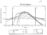
- FIG. 3 graphically indicates a rapid falloff in relative etch rate as a function of boron concentration using EDP as an etchant.
- the present invention is an etch-stop layer having a semiconductor layer having a first surface and a boron layer formed below the first surface of the semiconductor layer.
- the boron layer has a full-width half-maximum (FWHM) thickness value of less than 100 nanometers.
- the boron layer is formed by a chemical vapor deposition (CVD) system.
- the present invention is a method to fabricate an etch-stop.
- the method includes flowing a carrier gas over a substrate in a chemical vapor deposition chamber, flowing a silicon precursor gas over the substrate in the deposition chamber and flowing a boron precursor gas over the substrate in the deposition chamber.
- the boron precursor gas forms a boron layer to act as the etch-stop and forms below a first surface of the substrate.
- the boron layer is less than 100 nanometers in thickness when measured as a full-width half-maximum (FWHM) value.
- FWHM full-width half-maximum
- the present invention is a method to form an electronic device.
- the method includes flowing a boron precursor gas over a substrate in a chemical vapor deposition chamber such that the boron precursor gas forms a boron layer thereby acting as an etch-stop layer.
- the etch-stop layer is formed below a first surface of the substrate and is less than 100 nanometers in thickness when measured as a full-width half-maximum (FWHM) value.
- One or more dielectric spacers are formed on a surface of the substrate to provide a self-aligning structure.
- the one or more dielectric spacers are doped with carbon atoms.
- the carbon atoms are remotely injected from the one or more dielectric spacers by annealing the substrate, thereby allowing the carbon atoms to diffuse into the etch-stop layer.
- the present invention is an etch-stop layer comprising a semiconductor substrate having a first surface and a boron layer formed below the first surface of the semiconductor substrate.
- the boron layer has a full-width half-maximum (FWHM) thickness value of less than 100 nanometers and is formed by a chemical vapor deposition (CVD) system.
- a germanium profile comprised of germanium atoms is formed substantially within the boron layer and has a germanium fraction of less than one percent to about 20 percent.
- a carbon profile comprised of carbon atoms is formed substantially within the boron layer and has a concentration within the profile area of between 10 18 and 10 21 atoms per cubic centimeter.
- FIGS. 1A-1D are cross-sectional views of a prior art bond and etch back silicon on insulator (BESOI) fabrication technique.
- FIGS. 2A-2C are cross-sectional views indicating a method to determine etch-stop efficiency.
- FIG. 3 is a graph indicating relative etch rates for an ethylenediamine-pyrocatechol (EDP) wet-chemical etchant as a function of boron concentration contained within a silicon (100) substrate at different annealing temperatures.
- EDP ethylenediamine-pyrocatechol
- FIG. 4 is a graph indicating a diffusion constant of boron as a function of germanium content at 800° C.
- FIG. 5 is a graph indicating full-width half-maximum (FWHM) depth of a boron profile produced in accordance with the present invention and measured after thermal annealing steps.
- FWHM full-width half-maximum
- FIG. 6 is a graph indicating boron diffusion depth in SiGe:C:B at various anneal temperatures.
- FIG. 7 is a graph indicating boron diffusion profiles and relative depth in a remote carbon method.
- boron-doped nanoscale etch-stop Disclosed herein is a fabrication method and a structure resulting therefrom for a boron-doped nanoscale etch-stop.
- the boron is doped into either a silicon (Si) substrate or film, or a compound semiconductor substrate or film.
- the compound semiconductor film may be chosen from a Group III-V semiconductor compound such as SiGe, GaAs, or InGaAs.
- a Group II-VI semiconductor compound may be chosen such as ZnSe, CdSe, or CdTe.
- the boron-doped nanoscale etch-stop described herein has particular applications in BESOI processing. However, the disclosed boron etch-stop is not limited only to BESOI applications.
- a BESOI substrate fabricated in accordance with one exemplary embodiment of the present invention has particular applications in low-power and radiation-hardened CMOS devices.
- Incorporation of the present invention in various electronic devices simplifies certain fabrication processes, improves scalability of devices, improves sub-threshold slopes, and reduces parasitic capacitances.
- boron (B) is traditionally provided via ion implantation.
- a resulting boron etch-stop layer is very wide following thermal treatments.
- the width of the boron layer is due to boron outdiffusion during any thermal treatments performed subsequent to the implant.
- One subsequent thermal treatment is a high temperature bonding step of the layer transfer process in BESOI processing.
- the boron outdiffusion is greatly enhanced by transient enhanced diffusion (TED) due to lattice damage and a large presence of silicon interstitial (S I ) atoms.
- TED transient enhanced diffusion
- S I silicon interstitial
- Widths of boron in ion implanted profiles can be greater than 200 nm to 300 nm depending on chosen quantities of ion implant energy and dosage. Typically, high dosage requirements also lead to a great deal of concentration-dependent outdiffusion. Therefore, the transferred silicon device layer thickness can exhibit a very wide thickness range since the etch process itself will have a wide profile range over which to stop on the boron-doped layer. The wide layer range poses significant process integration problems, especially when forming a deep (or even a shallow) trench isolation region.
- An “as grown” boron profile remains very narrow (e.g., less than 100 nm) by forming an ultra-thin (for example, less than 100 nm) boron profile with chemical vapor deposition (CVD) instead of ion implantation and, in some embodiments, by including germanium and carbon.
- CVD chemical vapor deposition
- the boron profile in this case remains very narrow even after significant subsequent thermal treatments up to approximately 1000° C. for about 10 seconds or more. Details of exemplary CVD process steps are outlined below.
- Silicon interstitial pairing with boron results in a rate of diffusion that is generally much greater than occurs with boron alone.
- the intrinsic diffusion coefficient (D Si ) of silicon in silicon is approximately 560 whereas the intrinsic diffusion coefficient of boron (D B ) in silicon is approximately 1.
- Incorporating carbon (C) into boron-doped silicon minimizes a Si—B pair formation and thus reduces an overall rate of boron outdiffusion.
- the reduced boron outdiffusion results in less spreading of a p-type SiGe base region.
- Narrow base widths reduce transit times of minority carriers and improve a device shutoff frequency, f t .
- the boron diffusion can be effectively mitigated at temperatures of approximately 1000° C. for 10 seconds or longer.
- a device or substrate designer may prefer boron over carbon and/or Ge as a etch-stop depending on device requirements. For example, a design decision may be driven by a preferred majority carrier type and concentration, or a minority carrier type and concentration.
- a design decision may be driven by a preferred majority carrier type and concentration, or a minority carrier type and concentration.
- One skilled in the art will recognize that adding carbon to a boron-doped layer will diminish carrier mobility. Consequently, more boron is required to compensate for the diminished carrier effect.
- a skilled artisan will further recognize that the addition of Ge to form a strained lattice in elemental or compound semiconductors enhance in-plane majority carrier hole mobility, but diminishes in-plane majority carrier electron mobility. Therefore, if boron is added to a carbon and/or germanium-doped lattice, the fabrication process must be completely characterized. The process will be a function of gas flows, temperatures, and pressures.
- FIG. 4 indicates measured rates of intrinsic boron diffusivity at 800° C. as a function of Ge content, x, in Si 1-x Ge x .
- FIG. 5 is a profile graph 500 representing data from a secondary-ion mass spectrometry (SIMS) profile of boron diffusion in carbon and Ge-doped silicon.
- SIMS secondary-ion mass spectrometry
- a location of the Ge is illustrated by a lower 501 and an upper 503 vertical line positioned at 50 nm and 85 nm depths, respectively.
- the boron remains relatively fixed up to temperatures of 1000° C., then diffuses rapidly at higher temperatures (anneal times are 10 seconds at each temperature).
- anneal times are 10 seconds at each temperature.
- the presence of both carbon and Ge reduces boron outdiffusion.
- the presence of carbon and Ge reduces overall boron diffusion by a factor of ten or more.
- a graph 600 indicates boron diffusion depths in SiGe:C:B and a germanium fraction. Boron profiles are displayed in the graph 600 following growth of SiGe:C:B where the subsequent thermal anneals, in this example, relate to bond steps.
- the graph 600 indicates boron in SiGe with carbon substantially present throughout portions of the structure.
- the graph 600 is a complete carbon method for providing a narrow boron profile.
- a germanium fraction indicates an increased germanium profile substantially within the boron layer.
- the germanium fraction is within a range from less than one percent to about 20%.
- the profile width for the boron concentration at 1000° C. extends from roughly 62 nm to less than 82 nm. Consequently, the FWHM value is less than about 20 nm. Consequently, the etch-stop is on a nanoscale level.
- the boron etch-stop is formed by chemical vapor deposition (CVD) techniques.
- FIG. 7 illustrates an embodiment in which profiles of B, C, and Ge are shown with reference to a placement of outer spacers fabricated in a remote carbon injection method.
- carbon is only present in outer spacer regions as indicated.
- the spacer regions are comprised of SiGe.
- a remote carbon technique suitable for adding carbon in various embodiments described herein, is disclosed in U.S. patent application Ser. No. 11/166,287 filed Jun. 23, 2005, entitled “Method for Growth and Optimization of Heterojunction Bipolar Film Stacks by Remote Injection,” and commonly assigned, along with this application, to Atmel Corporation, San Jose, Calif.
- the Ser. No. 11/166,287 application is hereby incorporated by reference in its entirety.
- the remote carbon injection technique entails a carbon implantation or diffusion step in a semiconductor fabrication process to inject carbon atoms into, for example, a semiconductor device layer and surrounding regions.
- the carbon implantation or diffusion step may be performed into an insulting layer.
- the carbon is derived from a carbon precursor such as methyl silane (CH 3 SiH 3 ).
- Carbon precursor injection can be accomplished by techniques such as LPCVD (low pressure chemical vapor deposition), UHCVD (ultra-high vacuum CVD), MBE (molecular beam epitaxy), or ion implantation.
- the carbon injection is followed by a thermal anneal step.
- the thermal anneal step allows the carbon to diffuse into, for example, a base region of a transistor. Note that, even though a carbon precursor may be injected outside of the base region, the position of the carbon after anneal is within the base region due to an energetically favorable diffusion mechanism. Therefore, remote injection is a means of doping a semiconductor with carbon and provides numerous advantages over conventional fabrication methods, discussed above (e.g., preventing boron outdiffusion thus allowing a higher boron-dopant concentration). Therefore, a location of injection and not necessarily a final resting place of carbon following thermal cycles determines a definition of remote carbon injection.
- the remote injection can occur during or after growth of a base-emitter spacer (BE) or a base-collector spacer (BC).
- BE base-emitter spacer
- BC base-collector spacer
- Carbon injection may be performed at multiple points during fabrication of either the base, BC, BE, collector, and/or emitter regions.
- Thermal anneal cycles are then implemented to provide activation energy for the carbon to diffuse from the dielectric spacer into the one or more various semiconductor regions.
- a final position of carbon after anneal is within the semiconductor through a diffusion mechanism.
- Advantages of remote carbon injection thus include a reduced boron outdiffusion and a significant reduction in the transistor base resistance.
- etch-stop layer other than remote carbon injection
- general techniques for implementing these various techniques are described in detail, below.
- Various permutations of the general etch-stop fabrication method based on the methods disclosed herein may be employed.
- a boron etch-stop may be fabricated by in-situ boron doping of silicon by CVD in which the silicon contains neither germanium nor carbon.
- a boron etch-stop may be fabricated by in-situ boron doping of SiGe by CVD in which the SiGe contains no carbon.
- a boron etch-stop may be fabricated by in-situ boron doping of silicon-carbide (SiC) by CVD in which the SiC contains no germanium.
- the boron-doped semiconductor could be implanted by an ion implantation or molecular beam epitaxial (MBE) process.
- MBE molecular beam epitaxial
- a flash anneal e.g., from 900° C. to 1200° C. for 1 second to 5 seconds
- a laser anneal e.g., less than a one second pulse may be used in order to alleviate any ion implantation damage and still maintain a narrow distribution of boron.
- carbon and/or germanium may also be added.
- process conditions can vary widely depending upon particular devices fabricated, specific equipment types employed, and various combinations of starting materials. Also, as is known to a skilled artisan, various dopant profiles may be achieved by certain gases being injected simultaneously and/or ramping the gas flow rates.
- the process conditions entail flowing hydrogen (H 2 ) as a carrier gas in a chemical vapor deposition (CVD) system at a flow rate between 5 standard liters per minute (slpm) and 100 slpm.
- inert gases such as nitrogen (N 2 ), argon (Ar), helium (He), xenon (Xe), and fluorine (F 2 ) are all suitable carrier gases.
- Silane SiH 4
- Si 2 H 6 silicon precursor gas
- Disilane deposits silicon at a faster rate and lower temperature than silane.
- Diborane (B 2 H 6 ) may be used as a boron precursor gas, flowing at between 5 sccm and 1000 sccm. Additionally, boron trichloride (BCl 3 ) or any other boron precursor gas may be used in place of diborane. Methyl silane (CH 3 SiH 3 ), or another carbon precursor gas, flowing at between 5 sccm and 1000 sccm may be employed as the carbon precursor. Germanium tetrahydride (GeH 4 ) or another germanium precursor gas flowing at between 5 sccm and 1000 sccm may be employed as the germanium precursor gas.
- growth temperatures may be in an exemplary range of 550° C. to 750° C. with processing pressures from 1 Torr to 100 Torr.
Landscapes
- Engineering & Computer Science (AREA)
- Manufacturing & Machinery (AREA)
- Power Engineering (AREA)
- Microelectronics & Electronic Packaging (AREA)
- Computer Hardware Design (AREA)
- Physics & Mathematics (AREA)
- General Physics & Mathematics (AREA)
- Condensed Matter Physics & Semiconductors (AREA)
- Chemical & Material Sciences (AREA)
- General Chemical & Material Sciences (AREA)
- Chemical Kinetics & Catalysis (AREA)
- Bipolar Transistors (AREA)
- Chemical Vapour Deposition (AREA)
Abstract
Description
where RSi is an etch rate of silicon and Res is an etch rate of the etch-stop. Therefore, a selectivity value where S=1 relates to a case of no etch selectivity.
where t is the etch time required to reach the maximum etch step height h2. In the prior example, t2 is the etch time required to reach the maximum etch step height h2.
Claims (17)
Priority Applications (4)
| Application Number | Priority Date | Filing Date | Title |
|---|---|---|---|
| US11/553,313 US7569913B2 (en) | 2006-10-26 | 2006-10-26 | Boron etch-stop layer and methods related thereto |
| PCT/US2007/080772 WO2008057692A2 (en) | 2006-10-26 | 2007-10-09 | System and method for providing a nanoscale, highly selective, and thermally resilient boron etch-stop |
| TW096139739A TW200828431A (en) | 2006-10-26 | 2007-10-23 | System and method for providing a nanoscale, highly selective, and thermally resilient boron etch-stop |
| US12/114,571 US20080237716A1 (en) | 2006-10-26 | 2008-05-02 | Integrated circuit structures having a boron etch-stop layer and methods, devices and systems related thereto |
Applications Claiming Priority (1)
| Application Number | Priority Date | Filing Date | Title |
|---|---|---|---|
| US11/553,313 US7569913B2 (en) | 2006-10-26 | 2006-10-26 | Boron etch-stop layer and methods related thereto |
Related Child Applications (1)
| Application Number | Title | Priority Date | Filing Date |
|---|---|---|---|
| US12/114,571 Continuation US20080237716A1 (en) | 2006-10-26 | 2008-05-02 | Integrated circuit structures having a boron etch-stop layer and methods, devices and systems related thereto |
Publications (2)
| Publication Number | Publication Date |
|---|---|
| US20080099840A1 US20080099840A1 (en) | 2008-05-01 |
| US7569913B2 true US7569913B2 (en) | 2009-08-04 |
Family
ID=39329097
Family Applications (2)
| Application Number | Title | Priority Date | Filing Date |
|---|---|---|---|
| US11/553,313 Active US7569913B2 (en) | 2006-10-26 | 2006-10-26 | Boron etch-stop layer and methods related thereto |
| US12/114,571 Abandoned US20080237716A1 (en) | 2006-10-26 | 2008-05-02 | Integrated circuit structures having a boron etch-stop layer and methods, devices and systems related thereto |
Family Applications After (1)
| Application Number | Title | Priority Date | Filing Date |
|---|---|---|---|
| US12/114,571 Abandoned US20080237716A1 (en) | 2006-10-26 | 2008-05-02 | Integrated circuit structures having a boron etch-stop layer and methods, devices and systems related thereto |
Country Status (3)
| Country | Link |
|---|---|
| US (2) | US7569913B2 (en) |
| TW (1) | TW200828431A (en) |
| WO (1) | WO2008057692A2 (en) |
Cited By (10)
| Publication number | Priority date | Publication date | Assignee | Title |
|---|---|---|---|---|
| US20070054460A1 (en) * | 2005-06-23 | 2007-03-08 | Atmel Corporation | System and method for providing a nanoscale, highly selective, and thermally resilient silicon, germanium, or silicon-germanium etch-stop |
| US20080050883A1 (en) * | 2006-08-25 | 2008-02-28 | Atmel Corporation | Hetrojunction bipolar transistor (hbt) with periodic multilayer base |
| US20080237716A1 (en) * | 2006-10-26 | 2008-10-02 | Atmel Corporation | Integrated circuit structures having a boron etch-stop layer and methods, devices and systems related thereto |
| US8173526B2 (en) | 2006-10-31 | 2012-05-08 | Atmel Corporation | Method for providing a nanoscale, high electron mobility transistor (HEMT) on insulator |
| US8530934B2 (en) | 2005-11-07 | 2013-09-10 | Atmel Corporation | Integrated circuit structures containing a strain-compensated compound semiconductor layer and methods and systems related thereto |
| US20170148726A1 (en) * | 2015-11-03 | 2017-05-25 | Applied Materials, Inc. | Semiconductor processing method and semiconductor device |
| US9842913B1 (en) | 2016-05-18 | 2017-12-12 | Globalfoundries Inc. | Integrated circuit fabrication with boron etch-stop layer |
| US10249538B1 (en) | 2017-10-03 | 2019-04-02 | Globalfoundries Inc. | Method of forming vertical field effect transistors with different gate lengths and a resulting structure |
| US20210327754A1 (en) * | 2012-03-27 | 2021-10-21 | Novellus Systems, Inc. | Tungsten feature fill |
| US11978666B2 (en) | 2018-12-05 | 2024-05-07 | Lam Research Corporation | Void free low stress fill |
Families Citing this family (11)
| Publication number | Priority date | Publication date | Assignee | Title |
|---|---|---|---|---|
| US20060292809A1 (en) * | 2005-06-23 | 2006-12-28 | Enicks Darwin G | Method for growth and optimization of heterojunction bipolar transistor film stacks by remote injection |
| US20070102834A1 (en) * | 2005-11-07 | 2007-05-10 | Enicks Darwin G | Strain-compensated metastable compound base heterojunction bipolar transistor |
| US20070148890A1 (en) * | 2005-12-27 | 2007-06-28 | Enicks Darwin G | Oxygen enhanced metastable silicon germanium film layer |
| US20070262295A1 (en) * | 2006-05-11 | 2007-11-15 | Atmel Corporation | A method for manipulation of oxygen within semiconductor materials |
| US7495250B2 (en) * | 2006-10-26 | 2009-02-24 | Atmel Corporation | Integrated circuit structures having a boron- and carbon-doped etch-stop and methods, devices and systems related thereto |
| US8148230B2 (en) * | 2009-07-15 | 2012-04-03 | Sandisk 3D Llc | Method of making damascene diodes using selective etching methods |
| JP5554142B2 (en) * | 2010-05-14 | 2014-07-23 | 株式会社豊田中央研究所 | Method for vapor phase growth of semiconductor film |
| CN103189956B (en) * | 2010-09-15 | 2018-06-22 | 普莱克斯技术有限公司 | Extend the method for ion source life |
| KR101599162B1 (en) * | 2011-08-15 | 2016-03-02 | 킹 압둘라 유니버시티 오브 사이언스 앤드 테크놀로지 | Method for producing mechlnically flexible silicon substrate |
| US9466729B1 (en) | 2015-05-08 | 2016-10-11 | Qualcomm Incorporated | Etch stop region based fabrication of bonded semiconductor structures |
| US10163719B2 (en) * | 2015-12-15 | 2018-12-25 | Taiwan Semiconductor Manufacturing Company, Ltd. | Method of forming self-alignment contact |
Citations (50)
| Publication number | Priority date | Publication date | Assignee | Title |
|---|---|---|---|---|
| US4652183A (en) | 1979-02-16 | 1987-03-24 | United Technologies Corporation | Amorphous boron-carbon alloy tool bits and methods of making the same |
| US5155571A (en) | 1990-08-06 | 1992-10-13 | The Regents Of The University Of California | Complementary field effect transistors having strained superlattice structure |
| US5378901A (en) | 1991-12-24 | 1995-01-03 | Rohm, Co., Ltd. | Heterojunction bipolar transistor and method for producing the same |
| US5466949A (en) | 1994-08-04 | 1995-11-14 | Texas Instruments Incorporated | Silicon oxide germanium resonant tunneling |
| US5569538A (en) * | 1993-10-06 | 1996-10-29 | Texas Instruments Incorporated | Semiconductor-on-insulator structure and method for producing same |
| US5906708A (en) | 1994-11-10 | 1999-05-25 | Lawrence Semiconductor Research Laboratory, Inc. | Silicon-germanium-carbon compositions in selective etch processes |
| US5965931A (en) | 1993-04-19 | 1999-10-12 | The Board Of Regents Of The University Of California | Bipolar transistor having base region with coupled delta layers |
| US6165891A (en) | 1999-11-22 | 2000-12-26 | Chartered Semiconductor Manufacturing Ltd. | Damascene structure with reduced capacitance using a carbon nitride, boron nitride, or boron carbon nitride passivation layer, etch stop layer, and/or cap layer |
| US6323108B1 (en) | 1999-07-27 | 2001-11-27 | The United States Of America As Represented By The Secretary Of The Navy | Fabrication ultra-thin bonded semiconductor layers |
| US6399970B2 (en) | 1996-09-17 | 2002-06-04 | Matsushita Electric Industrial Co., Ltd. | FET having a Si/SiGeC heterojunction channel |
| US6512252B1 (en) | 1999-11-15 | 2003-01-28 | Matsushita Electric Industrial Co., Ltd. | Semiconductor device |
| US20030040130A1 (en) * | 2001-08-09 | 2003-02-27 | Mayur Abhilash J. | Method for selection of parameters for implant anneal of patterned semiconductor substrates and specification of a laser system |
| US6531369B1 (en) | 2000-03-01 | 2003-03-11 | Applied Micro Circuits Corporation | Heterojunction bipolar transistor (HBT) fabrication using a selectively deposited silicon germanium (SiGe) |
| US6552375B2 (en) | 2000-11-15 | 2003-04-22 | Leland S. Swanson | Blocking of boron diffusion through the emitter-emitter poly interface in PNP HBTs through use of a SiC layer at the top of the emitter epi layer |
| US20030080394A1 (en) | 2001-10-31 | 2003-05-01 | Babcock Jeffrey A. | Control of dopant diffusion from polysilicon emitters in bipolar integrated circuits |
| US20030082882A1 (en) | 2001-10-31 | 2003-05-01 | Babcock Jeffrey A. | Control of dopant diffusion from buried layers in bipolar integrated circuits |
| US20030132453A1 (en) | 2002-01-15 | 2003-07-17 | International Business Machines Corporation | Method to fabricate SiGe HBTs with controlled current gain and improved breakdown voltage characteristics |
| US20030146448A1 (en) | 2002-02-04 | 2003-08-07 | Conexant Systems, Inc. | Band gap compensated HBT |
| US6670542B2 (en) * | 1999-12-28 | 2003-12-30 | Sanyo Electric Co., Ltd. | Semiconductor device and manufacturing method thereof |
| US20040009649A1 (en) | 2002-07-12 | 2004-01-15 | Kub Francis J. | Wafer bonding of thinned electronic materials and circuits to high performance substrates |
| US6680494B2 (en) | 2000-03-16 | 2004-01-20 | Northrop Grumman Corporation | Ultra high speed heterojunction bipolar transistor having a cantilevered base |
| US20040031979A1 (en) | 2002-06-07 | 2004-02-19 | Amberwave Systems Corporation | Strained-semiconductor-on-insulator device structures |
| US20040079989A1 (en) | 2002-10-11 | 2004-04-29 | Nissan Motor Co., Ltd. | Insulated gate tunnel-injection device having heterojunction and method for manufacturing the same |
| US6744079B2 (en) | 2002-03-08 | 2004-06-01 | International Business Machines Corporation | Optimized blocking impurity placement for SiGe HBTs |
| US6750484B2 (en) | 1996-12-09 | 2004-06-15 | Nokia Corporation | Silicon germanium hetero bipolar transistor |
| US6759694B1 (en) | 2003-09-10 | 2004-07-06 | Industrial Technology Research Institute | Semiconductor phototransistor |
| US20040164336A1 (en) | 1998-11-24 | 2004-08-26 | Micron Technology, Inc. | Films doped with carbon for use in integrated circuit technology |
| US20040222486A1 (en) | 2003-05-09 | 2004-11-11 | International Business Machines Corporation | BiCMOS TECHNOLOGY ON SOI SUBSTRATES |
| US6855963B1 (en) | 2003-08-29 | 2005-02-15 | International Business Machines Corporation | Ultra high-speed Si/SiGe modulation-doped field effect transistors on ultra thin SOI/SGOI substrate |
| US20050051861A1 (en) | 2003-09-09 | 2005-03-10 | Industrial Technology Research Institute | Avalanche photo-detector with high saturation power and high gain-bandwidth product |
| US20050112857A1 (en) | 2003-11-25 | 2005-05-26 | International Business Machines Corporation | Ultra-thin silicidation-stop extensions in mosfet devices |
| US6906400B2 (en) | 2003-01-14 | 2005-06-14 | Interuniversitair Microelektronica Centrum (Imec) | SiGe strain relaxed buffer for high mobility devices and a method of fabricating it |
| US6927140B2 (en) | 2002-08-21 | 2005-08-09 | Intel Corporation | Method for fabricating a bipolar transistor base |
| US20050181555A1 (en) | 2000-03-07 | 2005-08-18 | Haukka Suvi P. | Thin films |
| US20050191911A1 (en) | 2004-02-27 | 2005-09-01 | International Business Machines Corporation | Transistor structure with minimized parasitics and method of fabricating the same |
| US20050230705A1 (en) | 2002-04-26 | 2005-10-20 | Taylor Geoff W | Thz detection employing modulation doped quantum well device structures |
| US6995430B2 (en) | 2002-06-07 | 2006-02-07 | Amberwave Systems Corporation | Strained-semiconductor-on-insulator device structures |
| US20060030093A1 (en) | 2004-08-06 | 2006-02-09 | Da Zhang | Strained semiconductor devices and method for forming at least a portion thereof |
| US20060068557A1 (en) | 2003-08-05 | 2006-03-30 | Fujitsu Limited | Semiconductor device and method for fabricating the same |
| US7091114B2 (en) * | 2002-04-16 | 2006-08-15 | Kabushiki Kaisha Toshiba | Semiconductor device and method of manufacturing the same |
| US20060231862A1 (en) | 2003-04-15 | 2006-10-19 | Nobuyuki Otsuka | Ballistic semiconductor device |
| US20060284165A1 (en) | 2005-04-19 | 2006-12-21 | The Ohio State University | Silicon-based backward diodes for zero-biased square law detection and detector arrays of same |
| US20060292809A1 (en) | 2005-06-23 | 2006-12-28 | Enicks Darwin G | Method for growth and optimization of heterojunction bipolar transistor film stacks by remote injection |
| US20070054460A1 (en) * | 2005-06-23 | 2007-03-08 | Atmel Corporation | System and method for providing a nanoscale, highly selective, and thermally resilient silicon, germanium, or silicon-germanium etch-stop |
| US20070096142A1 (en) | 2005-08-29 | 2007-05-03 | Kabushiki Kaisha Toshiba | Semiconductor device |
| US20070105335A1 (en) | 2005-11-01 | 2007-05-10 | Massachusetts Institute Of Technology | Monolithically integrated silicon and III-V electronics |
| US20070290193A1 (en) | 2006-01-18 | 2007-12-20 | The Board Of Trustees Of The University Of Illinois | Field effect transistor devices and methods |
| WO2008024587A2 (en) | 2006-08-25 | 2008-02-28 | Atmel Corporation | A heterojunction bipolar transistor (hbt) with periodic multi layer base |
| US20080099882A1 (en) | 2006-10-26 | 2008-05-01 | Atmel Corporation | System and method for providing a nanoscale, highly selective, and thermally resilient carbon etch-stop |
| US20080099840A1 (en) | 2006-10-26 | 2008-05-01 | Atmel Corporation | System and method for providing a nanoscale, highly selective, and thermally resilient boron etch-stop |
-
2006
- 2006-10-26 US US11/553,313 patent/US7569913B2/en active Active
-
2007
- 2007-10-09 WO PCT/US2007/080772 patent/WO2008057692A2/en active Search and Examination
- 2007-10-23 TW TW096139739A patent/TW200828431A/en unknown
-
2008
- 2008-05-02 US US12/114,571 patent/US20080237716A1/en not_active Abandoned
Patent Citations (70)
| Publication number | Priority date | Publication date | Assignee | Title |
|---|---|---|---|---|
| US4652183A (en) | 1979-02-16 | 1987-03-24 | United Technologies Corporation | Amorphous boron-carbon alloy tool bits and methods of making the same |
| US5155571A (en) | 1990-08-06 | 1992-10-13 | The Regents Of The University Of California | Complementary field effect transistors having strained superlattice structure |
| US5378901A (en) | 1991-12-24 | 1995-01-03 | Rohm, Co., Ltd. | Heterojunction bipolar transistor and method for producing the same |
| US5965931A (en) | 1993-04-19 | 1999-10-12 | The Board Of Regents Of The University Of California | Bipolar transistor having base region with coupled delta layers |
| US5569538A (en) * | 1993-10-06 | 1996-10-29 | Texas Instruments Incorporated | Semiconductor-on-insulator structure and method for producing same |
| US5466949A (en) | 1994-08-04 | 1995-11-14 | Texas Instruments Incorporated | Silicon oxide germanium resonant tunneling |
| US20020081861A1 (en) | 1994-11-10 | 2002-06-27 | Robinson Mcdonald | Silicon-germanium-carbon compositions and processes thereof |
| US5906708A (en) | 1994-11-10 | 1999-05-25 | Lawrence Semiconductor Research Laboratory, Inc. | Silicon-germanium-carbon compositions in selective etch processes |
| US6064081A (en) | 1994-11-10 | 2000-05-16 | Lawrence Semiconductor Research Laboratory, Inc. | Silicon-germanium-carbon compositions and processes thereof |
| US20020105015A1 (en) | 1996-09-17 | 2002-08-08 | Matsushita Electric Industrial Co., Ltd. | Semiconductor device and method of producing the same |
| US6399970B2 (en) | 1996-09-17 | 2002-06-04 | Matsushita Electric Industrial Co., Ltd. | FET having a Si/SiGeC heterojunction channel |
| US6750484B2 (en) | 1996-12-09 | 2004-06-15 | Nokia Corporation | Silicon germanium hetero bipolar transistor |
| US20040164336A1 (en) | 1998-11-24 | 2004-08-26 | Micron Technology, Inc. | Films doped with carbon for use in integrated circuit technology |
| US6323108B1 (en) | 1999-07-27 | 2001-11-27 | The United States Of America As Represented By The Secretary Of The Navy | Fabrication ultra-thin bonded semiconductor layers |
| US6512252B1 (en) | 1999-11-15 | 2003-01-28 | Matsushita Electric Industrial Co., Ltd. | Semiconductor device |
| US6165891A (en) | 1999-11-22 | 2000-12-26 | Chartered Semiconductor Manufacturing Ltd. | Damascene structure with reduced capacitance using a carbon nitride, boron nitride, or boron carbon nitride passivation layer, etch stop layer, and/or cap layer |
| US6670542B2 (en) * | 1999-12-28 | 2003-12-30 | Sanyo Electric Co., Ltd. | Semiconductor device and manufacturing method thereof |
| US6531369B1 (en) | 2000-03-01 | 2003-03-11 | Applied Micro Circuits Corporation | Heterojunction bipolar transistor (HBT) fabrication using a selectively deposited silicon germanium (SiGe) |
| US20050181555A1 (en) | 2000-03-07 | 2005-08-18 | Haukka Suvi P. | Thin films |
| US6680494B2 (en) | 2000-03-16 | 2004-01-20 | Northrop Grumman Corporation | Ultra high speed heterojunction bipolar transistor having a cantilevered base |
| US6552375B2 (en) | 2000-11-15 | 2003-04-22 | Leland S. Swanson | Blocking of boron diffusion through the emitter-emitter poly interface in PNP HBTs through use of a SiC layer at the top of the emitter epi layer |
| US20030040130A1 (en) * | 2001-08-09 | 2003-02-27 | Mayur Abhilash J. | Method for selection of parameters for implant anneal of patterned semiconductor substrates and specification of a laser system |
| US20030082882A1 (en) | 2001-10-31 | 2003-05-01 | Babcock Jeffrey A. | Control of dopant diffusion from buried layers in bipolar integrated circuits |
| US20030080394A1 (en) | 2001-10-31 | 2003-05-01 | Babcock Jeffrey A. | Control of dopant diffusion from polysilicon emitters in bipolar integrated circuits |
| US6656809B2 (en) | 2002-01-15 | 2003-12-02 | International Business Machines Corporation | Method to fabricate SiGe HBTs with controlled current gain and improved breakdown voltage characteristics |
| US20030132453A1 (en) | 2002-01-15 | 2003-07-17 | International Business Machines Corporation | Method to fabricate SiGe HBTs with controlled current gain and improved breakdown voltage characteristics |
| US20040063293A1 (en) | 2002-01-15 | 2004-04-01 | International Business Machines Corporation | Method to fabricate SiGe HBTs with controlled current gain and improved breakdown voltage characteristics |
| US20030146448A1 (en) | 2002-02-04 | 2003-08-07 | Conexant Systems, Inc. | Band gap compensated HBT |
| US6744079B2 (en) | 2002-03-08 | 2004-06-01 | International Business Machines Corporation | Optimized blocking impurity placement for SiGe HBTs |
| US20060273392A1 (en) * | 2002-04-16 | 2006-12-07 | Kabushiki Kaisha Toshiba | Semiconductor device and method of manufacturing the same |
| US7091114B2 (en) * | 2002-04-16 | 2006-08-15 | Kabushiki Kaisha Toshiba | Semiconductor device and method of manufacturing the same |
| US20050230705A1 (en) | 2002-04-26 | 2005-10-20 | Taylor Geoff W | Thz detection employing modulation doped quantum well device structures |
| US20060186510A1 (en) | 2002-06-07 | 2006-08-24 | Amberwave Systems Corporation | Strained-semiconductor-on-insulator bipolar device structures |
| US20050280103A1 (en) | 2002-06-07 | 2005-12-22 | Amberwave Systems Corporation | Strained-semiconductor-on-insulator finFET device structures |
| US20040031979A1 (en) | 2002-06-07 | 2004-02-19 | Amberwave Systems Corporation | Strained-semiconductor-on-insulator device structures |
| US7074623B2 (en) | 2002-06-07 | 2006-07-11 | Amberwave Systems Corporation | Methods of forming strained-semiconductor-on-insulator finFET device structures |
| US6995430B2 (en) | 2002-06-07 | 2006-02-07 | Amberwave Systems Corporation | Strained-semiconductor-on-insulator device structures |
| US20040009649A1 (en) | 2002-07-12 | 2004-01-15 | Kub Francis J. | Wafer bonding of thinned electronic materials and circuits to high performance substrates |
| US6927140B2 (en) | 2002-08-21 | 2005-08-09 | Intel Corporation | Method for fabricating a bipolar transistor base |
| US20040079989A1 (en) | 2002-10-11 | 2004-04-29 | Nissan Motor Co., Ltd. | Insulated gate tunnel-injection device having heterojunction and method for manufacturing the same |
| US6906400B2 (en) | 2003-01-14 | 2005-06-14 | Interuniversitair Microelektronica Centrum (Imec) | SiGe strain relaxed buffer for high mobility devices and a method of fabricating it |
| US20060231862A1 (en) | 2003-04-15 | 2006-10-19 | Nobuyuki Otsuka | Ballistic semiconductor device |
| US6936910B2 (en) | 2003-05-09 | 2005-08-30 | International Business Machines Corporation | BiCMOS technology on SOI substrates |
| US20040222486A1 (en) | 2003-05-09 | 2004-11-11 | International Business Machines Corporation | BiCMOS TECHNOLOGY ON SOI SUBSTRATES |
| US20060068557A1 (en) | 2003-08-05 | 2006-03-30 | Fujitsu Limited | Semiconductor device and method for fabricating the same |
| US6855963B1 (en) | 2003-08-29 | 2005-02-15 | International Business Machines Corporation | Ultra high-speed Si/SiGe modulation-doped field effect transistors on ultra thin SOI/SGOI substrate |
| US20050127392A1 (en) | 2003-08-29 | 2005-06-16 | International Business Machines Corporation | Ultra high-speed Si/SiGe modulation-doped field effect transistors on ultra thin SOI/SGOI substrate |
| US20050045905A1 (en) | 2003-08-29 | 2005-03-03 | International Business Machines Corporation | Ultra high-speed si/sige modulation-doped field effect transistors on ultra thin soi/sgoi substrate |
| US6963089B2 (en) | 2003-09-09 | 2005-11-08 | Industrial Technology Research Institute | Avalanche photo-detector with high saturation power and high gain-bandwidth product |
| US20050051861A1 (en) | 2003-09-09 | 2005-03-10 | Industrial Technology Research Institute | Avalanche photo-detector with high saturation power and high gain-bandwidth product |
| US6759694B1 (en) | 2003-09-10 | 2004-07-06 | Industrial Technology Research Institute | Semiconductor phototransistor |
| US20050112857A1 (en) | 2003-11-25 | 2005-05-26 | International Business Machines Corporation | Ultra-thin silicidation-stop extensions in mosfet devices |
| US20050191911A1 (en) | 2004-02-27 | 2005-09-01 | International Business Machines Corporation | Transistor structure with minimized parasitics and method of fabricating the same |
| US20060030093A1 (en) | 2004-08-06 | 2006-02-09 | Da Zhang | Strained semiconductor devices and method for forming at least a portion thereof |
| US20060284165A1 (en) | 2005-04-19 | 2006-12-21 | The Ohio State University | Silicon-based backward diodes for zero-biased square law detection and detector arrays of same |
| US20060292809A1 (en) | 2005-06-23 | 2006-12-28 | Enicks Darwin G | Method for growth and optimization of heterojunction bipolar transistor film stacks by remote injection |
| WO2007001672A2 (en) | 2005-06-23 | 2007-01-04 | Atmel Corporation | Growth of heterojunction bipolar trasistor stacks by remote injection |
| US20070054460A1 (en) * | 2005-06-23 | 2007-03-08 | Atmel Corporation | System and method for providing a nanoscale, highly selective, and thermally resilient silicon, germanium, or silicon-germanium etch-stop |
| US20070096142A1 (en) | 2005-08-29 | 2007-05-03 | Kabushiki Kaisha Toshiba | Semiconductor device |
| US20070105335A1 (en) | 2005-11-01 | 2007-05-10 | Massachusetts Institute Of Technology | Monolithically integrated silicon and III-V electronics |
| US20070290193A1 (en) | 2006-01-18 | 2007-12-20 | The Board Of Trustees Of The University Of Illinois | Field effect transistor devices and methods |
| WO2008024587A2 (en) | 2006-08-25 | 2008-02-28 | Atmel Corporation | A heterojunction bipolar transistor (hbt) with periodic multi layer base |
| US20080050883A1 (en) | 2006-08-25 | 2008-02-28 | Atmel Corporation | Hetrojunction bipolar transistor (hbt) with periodic multilayer base |
| US20080099882A1 (en) | 2006-10-26 | 2008-05-01 | Atmel Corporation | System and method for providing a nanoscale, highly selective, and thermally resilient carbon etch-stop |
| US20080099840A1 (en) | 2006-10-26 | 2008-05-01 | Atmel Corporation | System and method for providing a nanoscale, highly selective, and thermally resilient boron etch-stop |
| WO2008057692A2 (en) | 2006-10-26 | 2008-05-15 | Atmel Corporation | System and method for providing a nanoscale, highly selective, and thermally resilient boron etch-stop |
| WO2008057695A1 (en) | 2006-10-26 | 2008-05-15 | Atmel Corporation | A nanoscale, highly selective, thermally resilient carbon etch-stop |
| US20080237716A1 (en) | 2006-10-26 | 2008-10-02 | Atmel Corporation | Integrated circuit structures having a boron etch-stop layer and methods, devices and systems related thereto |
| US7495250B2 (en) | 2006-10-26 | 2009-02-24 | Atmel Corporation | Integrated circuit structures having a boron- and carbon-doped etch-stop and methods, devices and systems related thereto |
| WO2008054957A1 (en) | 2006-10-30 | 2008-05-08 | Atmel Corporation | System and method for providing a nanoscale, highly selective, and thermally resilient silicon, germanium, or silicon-germanium etch-stop |
Non-Patent Citations (38)
Cited By (12)
| Publication number | Priority date | Publication date | Assignee | Title |
|---|---|---|---|---|
| US20070054460A1 (en) * | 2005-06-23 | 2007-03-08 | Atmel Corporation | System and method for providing a nanoscale, highly selective, and thermally resilient silicon, germanium, or silicon-germanium etch-stop |
| US8530934B2 (en) | 2005-11-07 | 2013-09-10 | Atmel Corporation | Integrated circuit structures containing a strain-compensated compound semiconductor layer and methods and systems related thereto |
| US9012308B2 (en) | 2005-11-07 | 2015-04-21 | Atmel Corporation | Integrated circuit structures containing a strain-compensated compound semiconductor layer and methods and systems related thereto |
| US20080050883A1 (en) * | 2006-08-25 | 2008-02-28 | Atmel Corporation | Hetrojunction bipolar transistor (hbt) with periodic multilayer base |
| US20080237716A1 (en) * | 2006-10-26 | 2008-10-02 | Atmel Corporation | Integrated circuit structures having a boron etch-stop layer and methods, devices and systems related thereto |
| US8173526B2 (en) | 2006-10-31 | 2012-05-08 | Atmel Corporation | Method for providing a nanoscale, high electron mobility transistor (HEMT) on insulator |
| US20210327754A1 (en) * | 2012-03-27 | 2021-10-21 | Novellus Systems, Inc. | Tungsten feature fill |
| US20170148726A1 (en) * | 2015-11-03 | 2017-05-25 | Applied Materials, Inc. | Semiconductor processing method and semiconductor device |
| US9842913B1 (en) | 2016-05-18 | 2017-12-12 | Globalfoundries Inc. | Integrated circuit fabrication with boron etch-stop layer |
| US10224418B2 (en) | 2016-05-18 | 2019-03-05 | Globalfoundries Inc. | Integrated circuit fabrication with boron etch-stop layer |
| US10249538B1 (en) | 2017-10-03 | 2019-04-02 | Globalfoundries Inc. | Method of forming vertical field effect transistors with different gate lengths and a resulting structure |
| US11978666B2 (en) | 2018-12-05 | 2024-05-07 | Lam Research Corporation | Void free low stress fill |
Also Published As
| Publication number | Publication date |
|---|---|
| US20080099840A1 (en) | 2008-05-01 |
| WO2008057692A3 (en) | 2008-07-03 |
| US20080237716A1 (en) | 2008-10-02 |
| WO2008057692A2 (en) | 2008-05-15 |
| TW200828431A (en) | 2008-07-01 |
Similar Documents
| Publication | Publication Date | Title |
|---|---|---|
| US7569913B2 (en) | Boron etch-stop layer and methods related thereto | |
| US7550758B2 (en) | Method for providing a nanoscale, high electron mobility transistor (HEMT) on insulator | |
| US7495250B2 (en) | Integrated circuit structures having a boron- and carbon-doped etch-stop and methods, devices and systems related thereto | |
| US20070054460A1 (en) | System and method for providing a nanoscale, highly selective, and thermally resilient silicon, germanium, or silicon-germanium etch-stop | |
| US6723622B2 (en) | Method of forming a germanium film on a semiconductor substrate that includes the formation of a graded silicon-germanium buffer layer prior to the formation of a germanium layer | |
| US5540785A (en) | Fabrication of defect free silicon on an insulating substrate | |
| US6455871B1 (en) | SiGe MODFET with a metal-oxide film and method for fabricating the same | |
| US6362065B1 (en) | Blocking of boron diffusion through the emitter-emitter poly interface in PNP HBTs through use of a SiC layer at the top of the emitter epi layer | |
| US6316818B1 (en) | Vertical bipolar transistor including an extrinsic base with reduced roughness, and fabrication process | |
| US9484430B2 (en) | Back-end transistors with highly doped low-temperature contacts | |
| US6867428B1 (en) | Strained silicon NMOS having silicon source/drain extensions and method for its fabrication | |
| US10497627B2 (en) | Method of manufacturing a dopant transistor located vertically on the gate | |
| US7714361B2 (en) | Bipolar junction transistor having a high germanium concentration in a silicon-germanium layer and a method for forming the bipolar junction transistor | |
| US8227319B2 (en) | Bipolar junction transistor having a high germanium concentration in a silicon-germanium layer and a method for forming the bipolar junction transistor | |
| CN1322547C (en) | Process for preparing silicon-germanium material on insulator based on silicon-germanium / silicon structure separation-by-implantation-of-oxygen | |
| CN100336172C (en) | Silicon-germanium material structure on insulator prepared through improved separation-by-implantation-of-oxygen technique and process thereof | |
| Jung et al. | Application of RTP-CVD Technology to Ulsi Device Fabrication |
Legal Events
| Date | Code | Title | Description |
|---|---|---|---|
| AS | Assignment |
Owner name: ATMEL CORPORATION, CALIFORNIA Free format text: ASSIGNMENT OF ASSIGNORS INTEREST;ASSIGNOR:ENICKS, DARWIN G.;REEL/FRAME:018695/0372 Effective date: 20061024 |
|
| FEPP | Fee payment procedure |
Free format text: PAYER NUMBER DE-ASSIGNED (ORIGINAL EVENT CODE: RMPN); ENTITY STATUS OF PATENT OWNER: LARGE ENTITY Free format text: PAYOR NUMBER ASSIGNED (ORIGINAL EVENT CODE: ASPN); ENTITY STATUS OF PATENT OWNER: LARGE ENTITY |
|
| STCF | Information on status: patent grant |
Free format text: PATENTED CASE |
|
| FPAY | Fee payment |
Year of fee payment: 4 |
|
| AS | Assignment |
Owner name: MORGAN STANLEY SENIOR FUNDING, INC. AS ADMINISTRATIVE AGENT, NEW YORK Free format text: PATENT SECURITY AGREEMENT;ASSIGNOR:ATMEL CORPORATION;REEL/FRAME:031912/0173 Effective date: 20131206 Owner name: MORGAN STANLEY SENIOR FUNDING, INC. AS ADMINISTRAT Free format text: PATENT SECURITY AGREEMENT;ASSIGNOR:ATMEL CORPORATION;REEL/FRAME:031912/0173 Effective date: 20131206 |
|
| AS | Assignment |
Owner name: ATMEL CORPORATION, CALIFORNIA Free format text: TERMINATION AND RELEASE OF SECURITY INTEREST IN PATENT COLLATERAL;ASSIGNOR:MORGAN STANLEY SENIOR FUNDING, INC.;REEL/FRAME:038376/0001 Effective date: 20160404 |
|
| FPAY | Fee payment |
Year of fee payment: 8 |
|
| AS | Assignment |
Owner name: JPMORGAN CHASE BANK, N.A., AS ADMINISTRATIVE AGENT Free format text: SECURITY INTEREST;ASSIGNOR:ATMEL CORPORATION;REEL/FRAME:043440/0467 Effective date: 20170829 |
|
| AS | Assignment |
Owner name: JPMORGAN CHASE BANK, N.A., AS ADMINISTRATIVE AGENT, DELAWARE Free format text: SECURITY INTEREST;ASSIGNORS:MICROCHIP TECHNOLOGY INC.;SILICON STORAGE TECHNOLOGY, INC.;ATMEL CORPORATION;AND OTHERS;REEL/FRAME:053311/0305 Effective date: 20200327 |
|
| AS | Assignment |
Owner name: MICROCHIP TECHNOLOGY INC., ARIZONA Free format text: RELEASE BY SECURED PARTY;ASSIGNOR:JPMORGAN CHASE BANK, N.A, AS ADMINISTRATIVE AGENT;REEL/FRAME:053466/0011 Effective date: 20200529 Owner name: SILICON STORAGE TECHNOLOGY, INC., ARIZONA Free format text: RELEASE BY SECURED PARTY;ASSIGNOR:JPMORGAN CHASE BANK, N.A, AS ADMINISTRATIVE AGENT;REEL/FRAME:053466/0011 Effective date: 20200529 Owner name: MICROSEMI STORAGE SOLUTIONS, INC., ARIZONA Free format text: RELEASE BY SECURED PARTY;ASSIGNOR:JPMORGAN CHASE BANK, N.A, AS ADMINISTRATIVE AGENT;REEL/FRAME:053466/0011 Effective date: 20200529 Owner name: ATMEL CORPORATION, ARIZONA Free format text: RELEASE BY SECURED PARTY;ASSIGNOR:JPMORGAN CHASE BANK, N.A, AS ADMINISTRATIVE AGENT;REEL/FRAME:053466/0011 Effective date: 20200529 Owner name: MICROSEMI CORPORATION, CALIFORNIA Free format text: RELEASE BY SECURED PARTY;ASSIGNOR:JPMORGAN CHASE BANK, N.A, AS ADMINISTRATIVE AGENT;REEL/FRAME:053466/0011 Effective date: 20200529 |
|
| AS | Assignment |
Owner name: WELLS FARGO BANK, NATIONAL ASSOCIATION, MINNESOTA Free format text: SECURITY INTEREST;ASSIGNORS:MICROCHIP TECHNOLOGY INC.;SILICON STORAGE TECHNOLOGY, INC.;ATMEL CORPORATION;AND OTHERS;REEL/FRAME:053468/0705 Effective date: 20200529 |
|
| AS | Assignment |
Owner name: WELLS FARGO BANK, NATIONAL ASSOCIATION, AS COLLATERAL AGENT, MINNESOTA Free format text: SECURITY INTEREST;ASSIGNORS:MICROCHIP TECHNOLOGY INCORPORATED;SILICON STORAGE TECHNOLOGY, INC.;ATMEL CORPORATION;AND OTHERS;REEL/FRAME:055671/0612 Effective date: 20201217 |
|
| MAFP | Maintenance fee payment |
Free format text: PAYMENT OF MAINTENANCE FEE, 12TH YEAR, LARGE ENTITY (ORIGINAL EVENT CODE: M1553); ENTITY STATUS OF PATENT OWNER: LARGE ENTITY Year of fee payment: 12 |
|
| AS | Assignment |
Owner name: WELLS FARGO BANK, NATIONAL ASSOCIATION, AS NOTES COLLATERAL AGENT, MINNESOTA Free format text: SECURITY INTEREST;ASSIGNORS:MICROCHIP TECHNOLOGY INCORPORATED;SILICON STORAGE TECHNOLOGY, INC.;ATMEL CORPORATION;AND OTHERS;REEL/FRAME:057935/0474 Effective date: 20210528 |
|
| AS | Assignment |
Owner name: ATMEL CORPORATION, ARIZONA Free format text: RELEASE BY SECURED PARTY;ASSIGNOR:JPMORGAN CHASE BANK, N.A., AS ADMINISTRATIVE AGENT;REEL/FRAME:059114/0333 Effective date: 20220218 |
|
| AS | Assignment |
Owner name: MICROSEMI STORAGE SOLUTIONS, INC., ARIZONA Free format text: RELEASE BY SECURED PARTY;ASSIGNOR:WELLS FARGO BANK, NATIONAL ASSOCIATION, AS NOTES COLLATERAL AGENT;REEL/FRAME:059863/0400 Effective date: 20220228 Owner name: MICROSEMI CORPORATION, ARIZONA Free format text: RELEASE BY SECURED PARTY;ASSIGNOR:WELLS FARGO BANK, NATIONAL ASSOCIATION, AS NOTES COLLATERAL AGENT;REEL/FRAME:059863/0400 Effective date: 20220228 Owner name: ATMEL CORPORATION, ARIZONA Free format text: RELEASE BY SECURED PARTY;ASSIGNOR:WELLS FARGO BANK, NATIONAL ASSOCIATION, AS NOTES COLLATERAL AGENT;REEL/FRAME:059863/0400 Effective date: 20220228 Owner name: SILICON STORAGE TECHNOLOGY, INC., ARIZONA Free format text: RELEASE BY SECURED PARTY;ASSIGNOR:WELLS FARGO BANK, NATIONAL ASSOCIATION, AS NOTES COLLATERAL AGENT;REEL/FRAME:059863/0400 Effective date: 20220228 Owner name: MICROCHIP TECHNOLOGY INCORPORATED, ARIZONA Free format text: RELEASE BY SECURED PARTY;ASSIGNOR:WELLS FARGO BANK, NATIONAL ASSOCIATION, AS NOTES COLLATERAL AGENT;REEL/FRAME:059863/0400 Effective date: 20220228 |
|
| AS | Assignment |
Owner name: MICROSEMI STORAGE SOLUTIONS, INC., ARIZONA Free format text: RELEASE BY SECURED PARTY;ASSIGNOR:WELLS FARGO BANK, NATIONAL ASSOCIATION, AS NOTES COLLATERAL AGENT;REEL/FRAME:059363/0001 Effective date: 20220228 Owner name: MICROSEMI CORPORATION, ARIZONA Free format text: RELEASE BY SECURED PARTY;ASSIGNOR:WELLS FARGO BANK, NATIONAL ASSOCIATION, AS NOTES COLLATERAL AGENT;REEL/FRAME:059363/0001 Effective date: 20220228 Owner name: ATMEL CORPORATION, ARIZONA Free format text: RELEASE BY SECURED PARTY;ASSIGNOR:WELLS FARGO BANK, NATIONAL ASSOCIATION, AS NOTES COLLATERAL AGENT;REEL/FRAME:059363/0001 Effective date: 20220228 Owner name: SILICON STORAGE TECHNOLOGY, INC., ARIZONA Free format text: RELEASE BY SECURED PARTY;ASSIGNOR:WELLS FARGO BANK, NATIONAL ASSOCIATION, AS NOTES COLLATERAL AGENT;REEL/FRAME:059363/0001 Effective date: 20220228 Owner name: MICROCHIP TECHNOLOGY INCORPORATED, ARIZONA Free format text: RELEASE BY SECURED PARTY;ASSIGNOR:WELLS FARGO BANK, NATIONAL ASSOCIATION, AS NOTES COLLATERAL AGENT;REEL/FRAME:059363/0001 Effective date: 20220228 |
|
| AS | Assignment |
Owner name: MICROSEMI STORAGE SOLUTIONS, INC., ARIZONA Free format text: RELEASE BY SECURED PARTY;ASSIGNOR:WELLS FARGO BANK, NATIONAL ASSOCIATION, AS NOTES COLLATERAL AGENT;REEL/FRAME:060894/0437 Effective date: 20220228 Owner name: MICROSEMI CORPORATION, ARIZONA Free format text: RELEASE BY SECURED PARTY;ASSIGNOR:WELLS FARGO BANK, NATIONAL ASSOCIATION, AS NOTES COLLATERAL AGENT;REEL/FRAME:060894/0437 Effective date: 20220228 Owner name: ATMEL CORPORATION, ARIZONA Free format text: RELEASE BY SECURED PARTY;ASSIGNOR:WELLS FARGO BANK, NATIONAL ASSOCIATION, AS NOTES COLLATERAL AGENT;REEL/FRAME:060894/0437 Effective date: 20220228 Owner name: SILICON STORAGE TECHNOLOGY, INC., ARIZONA Free format text: RELEASE BY SECURED PARTY;ASSIGNOR:WELLS FARGO BANK, NATIONAL ASSOCIATION, AS NOTES COLLATERAL AGENT;REEL/FRAME:060894/0437 Effective date: 20220228 Owner name: MICROCHIP TECHNOLOGY INCORPORATED, ARIZONA Free format text: RELEASE BY SECURED PARTY;ASSIGNOR:WELLS FARGO BANK, NATIONAL ASSOCIATION, AS NOTES COLLATERAL AGENT;REEL/FRAME:060894/0437 Effective date: 20220228 |