US7490283B2 - Pipelined data relocation and improved chip architectures - Google Patents
Pipelined data relocation and improved chip architectures Download PDFInfo
- Publication number
- US7490283B2 US7490283B2 US10/846,289 US84628904A US7490283B2 US 7490283 B2 US7490283 B2 US 7490283B2 US 84628904 A US84628904 A US 84628904A US 7490283 B2 US7490283 B2 US 7490283B2
- Authority
- US
- United States
- Prior art keywords
- data
- memory
- controller
- registers
- register
- Prior art date
- Legal status (The legal status is an assumption and is not a legal conclusion. Google has not performed a legal analysis and makes no representation as to the accuracy of the status listed.)
- Active, expires
Links
- 230000015654 memory Effects 0.000 claims abstract description 198
- 238000000034 method Methods 0.000 claims abstract description 90
- 238000012937 correction Methods 0.000 claims abstract description 47
- 239000000872 buffer Substances 0.000 claims description 64
- 238000012546 transfer Methods 0.000 claims description 51
- 238000013500 data storage Methods 0.000 claims description 16
- 238000001514 detection method Methods 0.000 claims description 9
- 230000004044 response Effects 0.000 claims description 6
- 238000013524 data verification Methods 0.000 claims description 2
- 230000006872 improvement Effects 0.000 abstract description 8
- 230000008569 process Effects 0.000 description 66
- 238000010586 diagram Methods 0.000 description 11
- 238000003491 array Methods 0.000 description 7
- 230000006870 function Effects 0.000 description 7
- 238000007667 floating Methods 0.000 description 5
- 230000008901 benefit Effects 0.000 description 4
- 230000007246 mechanism Effects 0.000 description 4
- 230000007547 defect Effects 0.000 description 3
- 102100027063 Overexpressed in colon carcinoma 1 protein Human genes 0.000 description 2
- 101710120324 Overexpressed in colon carcinoma 1 protein homolog Proteins 0.000 description 2
- 239000002131 composite material Substances 0.000 description 2
- 238000013461 design Methods 0.000 description 2
- 238000005516 engineering process Methods 0.000 description 2
- 238000002955 isolation Methods 0.000 description 2
- 230000008672 reprogramming Effects 0.000 description 2
- 239000004065 semiconductor Substances 0.000 description 2
- 238000013519 translation Methods 0.000 description 2
- 238000012795 verification Methods 0.000 description 2
- OKTJSMMVPCPJKN-UHFFFAOYSA-N Carbon Chemical compound [C] OKTJSMMVPCPJKN-UHFFFAOYSA-N 0.000 description 1
- 229910052799 carbon Inorganic materials 0.000 description 1
- 238000004891 communication Methods 0.000 description 1
- 230000008878 coupling Effects 0.000 description 1
- 238000010168 coupling process Methods 0.000 description 1
- 238000005859 coupling reaction Methods 0.000 description 1
- 238000013523 data management Methods 0.000 description 1
- 230000003247 decreasing effect Effects 0.000 description 1
- 230000003111 delayed effect Effects 0.000 description 1
- 238000010348 incorporation Methods 0.000 description 1
- 238000012005 ligant binding assay Methods 0.000 description 1
- 230000007774 longterm Effects 0.000 description 1
- 238000007726 management method Methods 0.000 description 1
- 230000013011 mating Effects 0.000 description 1
- 239000000203 mixture Substances 0.000 description 1
- 238000012986 modification Methods 0.000 description 1
- 230000004048 modification Effects 0.000 description 1
- 230000003287 optical effect Effects 0.000 description 1
- 238000005457 optimization Methods 0.000 description 1
- 238000012545 processing Methods 0.000 description 1
Images


Classifications
-
- G—PHYSICS
- G11—INFORMATION STORAGE
- G11C—STATIC STORES
- G11C7/00—Arrangements for writing information into, or reading information out from, a digital store
- G11C7/10—Input/output [I/O] data interface arrangements, e.g. I/O data control circuits, I/O data buffers
- G11C7/1015—Read-write modes for single port memories, i.e. having either a random port or a serial port
- G11C7/1039—Read-write modes for single port memories, i.e. having either a random port or a serial port using pipelining techniques, i.e. using latches between functional memory parts, e.g. row/column decoders, I/O buffers, sense amplifiers
-
- G—PHYSICS
- G06—COMPUTING; CALCULATING OR COUNTING
- G06F—ELECTRIC DIGITAL DATA PROCESSING
- G06F12/00—Accessing, addressing or allocating within memory systems or architectures
- G06F12/02—Addressing or allocation; Relocation
- G06F12/0223—User address space allocation, e.g. contiguous or non contiguous base addressing
- G06F12/023—Free address space management
- G06F12/0238—Memory management in non-volatile memory, e.g. resistive RAM or ferroelectric memory
- G06F12/0246—Memory management in non-volatile memory, e.g. resistive RAM or ferroelectric memory in block erasable memory, e.g. flash memory
-
- G—PHYSICS
- G11—INFORMATION STORAGE
- G11C—STATIC STORES
- G11C29/00—Checking stores for correct operation ; Subsequent repair; Testing stores during standby or offline operation
-
- G—PHYSICS
- G06—COMPUTING; CALCULATING OR COUNTING
- G06F—ELECTRIC DIGITAL DATA PROCESSING
- G06F11/00—Error detection; Error correction; Monitoring
- G06F11/07—Responding to the occurrence of a fault, e.g. fault tolerance
- G06F11/08—Error detection or correction by redundancy in data representation, e.g. by using checking codes
- G06F11/10—Adding special bits or symbols to the coded information, e.g. parity check, casting out 9's or 11's
- G06F11/1008—Adding special bits or symbols to the coded information, e.g. parity check, casting out 9's or 11's in individual solid state devices
-
- G—PHYSICS
- G06—COMPUTING; CALCULATING OR COUNTING
- G06F—ELECTRIC DIGITAL DATA PROCESSING
- G06F9/00—Arrangements for program control, e.g. control units
- G06F9/06—Arrangements for program control, e.g. control units using stored programs, i.e. using an internal store of processing equipment to receive or retain programs
- G06F9/30—Arrangements for executing machine instructions, e.g. instruction decode
- G06F9/38—Concurrent instruction execution, e.g. pipeline or look ahead
-
- G—PHYSICS
- G11—INFORMATION STORAGE
- G11C—STATIC STORES
- G11C16/00—Erasable programmable read-only memories
- G11C16/02—Erasable programmable read-only memories electrically programmable
- G11C16/06—Auxiliary circuits, e.g. for writing into memory
- G11C16/34—Determination of programming status, e.g. threshold voltage, overprogramming or underprogramming, retention
- G11C16/3436—Arrangements for verifying correct programming or erasure
-
- G—PHYSICS
- G11—INFORMATION STORAGE
- G11C—STATIC STORES
- G11C7/00—Arrangements for writing information into, or reading information out from, a digital store
- G11C7/10—Input/output [I/O] data interface arrangements, e.g. I/O data control circuits, I/O data buffers
-
- G—PHYSICS
- G11—INFORMATION STORAGE
- G11C—STATIC STORES
- G11C7/00—Arrangements for writing information into, or reading information out from, a digital store
- G11C7/10—Input/output [I/O] data interface arrangements, e.g. I/O data control circuits, I/O data buffers
- G11C7/1051—Data output circuits, e.g. read-out amplifiers, data output buffers, data output registers, data output level conversion circuits
Definitions
- Flash EEPROM devices are composed of one or more arrays of transistor cells, each cell capable of non-volatile storage of one or more bits of data. Thus flash memory does not require power to retain the data programmed therein. Once programmed however, a cell must be erased before it can be reprogrammed with a new data value.
- These arrays of cells are partitioned into groups to provide for efficient implementation of read, program and erase functions.
- a typical flash memory architecture for mass storage arranges large groups of cells into erasable blocks, wherein a block contains the smallest number of cells (unit of erase) that are erasable at one time.
- each block contains enough cells to store one sector of user data plus some overhead data related to the user data and/or to the block in which it is stored.
- the amount of user data included in a sector is the standard 512 bytes in one class of such memory systems but can be of some other size. Because the isolation of individual blocks of cells from one another that is required to make them individually erasable takes space on the integrated circuit chip, another class of flash memories makes the blocks significantly larger so there is less space required for such isolation.
- the subsystem controller in a large block system performs a number of functions including the translation between logical addresses (LBAs) received by the memory sub-system from a host, and physical block numbers (PBNs) and page addresses within the memory cell array. This translation often involves use of intermediate terms for a logical block number (LBN) and logical page.
- LBAs logical addresses
- PBNs physical block numbers
- the controller also manages the low level flash circuit operation through a series of commands that it issues to the flash memory devices via an interface bus. Another function the controller performs is to maintain the integrity of data stored to the subsystem through various means, such as by using an error correction code (ECC).
- ECC error correction code
- FIG. 1 shows a typical internal architecture for a flash memory device 131 .
- the primary features include an input/output (I/O) bus 411 and control signals 412 to interface to an external controller, a memory control circuit 450 to control internal memory operations with registers for command, address and status signals.
- One or more arrays 400 of flash EEPROM cells are included, each array having its own row decoder (XDEC) 401 and column decoder (YDEC) 402 , a group of sense amplifiers and program control circuitry (SA/PROG) 454 and a data register 404 .
- the memory cells usually include one or more conductive floating gates as storage elements but other long term electron charge storage elements may be used instead.
- the memory cell array may be operated with two levels of charge defined for each storage element to therefore store one bit of data with each element. Alternatively, more than two storage states may be defined for each storage element, in which case more than one bit of data is stored in each element.
- the external interface I/O bus 411 and control signals 412 can include the following:
- the memory have a means by which the storage subsystem controller may determine that the memory is busy performing some task.
- Such means could include a dedicated signal or a status bit in an internal memory register that is accessible while the memory is busy.
- FIG. 1 shows only one flash memory array 400 with its related components, but a multiplicity of such arrays can exist on a single flash memory chip that share a common interface and memory control circuitry but have separate XDEC 401 , YDEC 402 , SA/PROG 454 and DATA REG 404 circuitry in order to allow parallel read and program operations. More generally, there may be one or two additional such data registers typically arranged into the sort of master slave arrangements developed further in U.S. Pat. No. 6,560,143, which is hereby incorporated by reference. Another arrangement for a flash memory architecture using multiple data buffers is described in U.S. Pat. No. 5,822,245.
- Data is transferred from the memory array through the data register 404 to an external controller via the data registers' coupling to the I/O bus AD[7:0] 411 .
- the data register 404 is also coupled with/to the sense amplifier/programming circuit 454 .
- the data registers 404 can similarly be connected/coupled to the same sense amplifier/programming circuit 454 .
- the number of elements of the data register coupled to each sense amplifier/programming circuit element may depend on the number of bits stored in each storage element of the memory cells, flash EEPROM cells each containing one or more floating gates as the storage elements.
- Each storage element may store a plurality of bits, such as 2 or 4, if the memory cells are operated in a multi-state mode. Alternatively, the memory cells may be operated in a binary mode to store one bit of data per storage element.
- the row decoder 401 decodes row addresses for the array 400 in order to select the physical page to be accessed.
- the row decoder 401 receives row addresses via internal row address lines 419 from the memory control logic 450 .
- a column decoder 402 receives column addresses via internal column address lines 429 from the memory control logic 450 .
- FIG. 2 shows an architecture of a typical non-volatile data storage system, in this case employing flash memory cells as the storage media.
- this system is encapsulated within a removable card having an electrical connector extending along one side to provide the host interface when inserted into a receptacle of a host.
- the system of FIG. 2 may be embedded into a host system in the form of a permanently installed embedded circuit or otherwise.
- the system utilizes a single controller 101 that performs high-level host and memory control functions.
- the flash memory media is composed of one or more flash memory devices, each such device often formed on its own integrated circuit chip.
- the system controller and the flash memory are connected by a bus 121 that allows the controller 101 to load command, address, and transfer data to and from the flash memory array.
- the bus 121 includes 412 and 411 of FIG. 1 .
- the controller 101 interfaces with a host system (not shown) with which user data is transferred to and from the flash memory array.
- a host system (not shown) with which user data is transferred to and from the flash memory array.
- the host interface includes a mating plug and socket assembly (not shown) on the card and host equipment.
- the controller 101 receives a command from the host to read or write one or more sectors of user data starting at a particular logical address. This address may or may not align with the first physical page in a block of memory cells.
- Such non-volatile memory systems include one or more arrays of floating-gate memory cells and a system controller.
- the controller manages communication with the host system and operation of the memory cell array to store and retrieve user data.
- the memory cells are grouped together into blocks of cells, a block of cells being the smallest grouping of cells that are simultaneously erasable. Prior to writing data into one or more blocks of cells, those blocks of cells are erased.
- User data are typically transferred between the host and memory array in sectors.
- a sector of user data can be any amount that is convenient to handle, preferably less than the capacity of the memory block, often being equal to the standard disk drive sector size, 512 bytes.
- the memory system block is sized to store one sector of user data plus overhead data, the overhead data including information such as an error correction code (ECC) for the user data stored in the block, a history of use of the block, defects and other physical information of the memory cell block.
- ECC error correction code
- Another type of non-volatile memory system utilizes a larger memory cell block size that stores multiple sectors of user data.
- One architecture of the memory cell array conveniently forms a block from one or two rows of memory cells that are within a sub-array or other unit of cells and which share a common erase gate.
- it is currently most common to store one bit of data in each floating gate cell by defining only two programmed threshold levels the trend is to store more than one bit of data in each cell by establishing more than two floating-gate transistor threshold ranges.
- a memory system that stores two bits of data per floating gate (four threshold level ranges or states) is currently available, with three bits per cell (eight threshold level ranges or states) and four bits per cell (sixteen threshold level ranges) being contemplated for future systems.
- the number of memory cells required to store a sector of data goes down as the number of bits stored in each cell goes up. This trend, combined with a scaling of the array resulting from improvements in cell structure and general semiconductor processing, makes it practical to form a memory cell block in a segmented portion of a row of cells.
- the block structure can also be formed to enable selection of operation of each of the memory cells in two states (one data bit per cell) or in some multiple such as four states (two data bits per cell), as described in SanDisk Corporation U.S. Pat. No. 5,930,167, which is incorporated herein in its entirety by this reference.
- This data relocation time is a main contributor to all garbage collection routines.
- Prior art methods describe the data relocation operation as a consecutive data read, then data integrity check and error correction, if necessary, before writing the data to a new location, so that there is a high constant performance penalty of data transfer and verification. In the case of data error, additional time must be spent to correct the data before write.
- FIG. 3 An example of a simple copy sequence in the prior art, where the data is checked/corrected before being reprogrammed, is shown in FIG. 3 .
- This shows a first set of data (DATA 1 ) sequentially being read from memory 400 into data register 404 (R), then the read of the buffer by the controller (RB), the data being checked and any errors corrected (EC) in the controller, the writing the checked/corrected data from the buffer (WB) back to the register 404 , from where it is programmed (Program) back into the memory array 400 .
- DATA 1 data register 404
- RB data register 404
- EC data being checked and any errors corrected
- the data set is buffered in the controller, it can then be checked/corrected for error (E); however, even though there will now be a corrected set of data in the controller that can be supplied to the host, if there are errors to correct, these errors are written back to the memory as programming has begun before the data set has been checked and corrected. As with the process of FIG. 3 , the entire process of FIG. 4 has to be completed each set of data before it can begin for the subsequent data set.
- a data relocation method is presented which allows the correction of data errors during garbage collection operations without any penalty to overall performance and time-out/latency in defect tolerant systems, thereby allowing the usage of flash memory with higher error rate in performance critical applications.
- improved memory architectures allows data transfers between controller and the memory concurrently with read and program operations, thus accelerating complex data operations such as data relocation, or garbage collection, and write-read back-verify processes, particularly for systems with high error rate memories.
- the invention describes a method of pipelined relocation of multiple data portions, where an integrity check and error correction of a current data portion is done concurrently with the programming of the previous data portion.
- a flash/EEPROM memory chip has two data registers, where one register can read out data from the memory array while the other is used for programming operations of data to the memory cell array. Every register has a capacity of up to one memory page and can be used by individual data transfer commands Read Register and Write.
- This architecture also provides mechanism for internal, on-chip, pipelining of other complex data operations such as Write-Read Back-Verify.
- FIG. 1 is a block diagram of a typical prior art flash EEPROM memory array with memory control logic, data and address registers.
- FIG. 2 illustrates an architecture utilizing memories of FIG. 1 with a system controller.
- FIG. 3 shows an example of a simple copy sequence in the prior art.
- FIG. 4 shows an example of a copy sequence in the prior art where each data set is checked after the start of programming.
- FIG. 5 illustrates a first memory architecture in which the present invention can be implemented.
- FIG. 6 illustrates a second memory architecture in which the present invention can be implemented.
- FIG. 7 shows features of the embodiment of FIG. 6 .
- FIG. 8 illustrates another memory architecture in which the present invention can be implemented.
- FIGS. 9 and 10 illustrate the general concept of pipelining data relocation operations.
- FIG. 11 explains some of the notation used in FIGS. 13-15 , 17 , and 18 .
- FIG. 12 summarizes the operations specific to the different memory architectures.
- FIGS. 13-15 illustrate several basic on chip copy functions using aspects of the present invention.
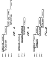
- FIG. 16 shows an embodiment of the present invention based upon the architecture of FIG. 5 .
- FIGS. 17 and 18 isolate aspects of the present invention that may used in an embodiment based on the architecture of FIG. 5 .
- FIG. 19 shows an embodiment combining aspects of FIGS. 13 and 14 .
- FIG. 20 shows a prior art Write-Read back-Verify operation.
- FIG. 21 shows a Write-Read back-Verify operation according to the present invention.
- FIG. 22 shows a pipelined chip-to-chip copy process.
- FIG. 23 shows the pipelining of on-chip copy processes from multiple chips, where the copy process on each chip is itself pipelined.
- the present invention describes a data relocation method that allows correction of data errors during garbage collection operations without any penalty to overall performance and time-out/latency in defect tolerant systems, and thus, allows usage of flash memory with higher error rate in performance critical applications.
- Other aspects are improved flash chip architectures that allows data transfers between controller and flash chip concurrently with read and program operations, thus accelerating complex data operations, like data relocation (garbage collection) and Write-Read Back-Verify, typical for systems with high error rate memory.
- the various aspects of the present invention are applicable to non-volatile memory systems in general.
- the description below, as well as that in the Background, is given mainly in terms of an EEPROM Flash memory embodiment
- the particular type of storage unit used in the memory array is not particularly important in the present invention.
- the particulars of how the storage elements are read, are written, and store data do not enter in to the main aspects of the present invention and can be those of any of the various non-volatile systems.
- an exemplary flash/EEPROM memory chip has two independent data buffers, where each buffer can be used for data access by the user while the other is used for program or read operations of data to or from the memory cell array. Every buffer has a capacity of up to one memory page and can be used by individual data transfer commands Read Buffer and Write. The above data transfer commands can be executed simultaneously with flash memory being programmed or read. The read and program commands are also specific for each buffer.
- FIGS. 5-8 show various architectures that are both aspects of the present invention themselves and allow other aspects of the present invention to be implemented.
- Each of these Figures shows a memory system including a controller 111 having one or more data buffers ( 111 , 111 a , 111 b ) connected to a memory 131 having an array 133 of non-volatile memory cells and one or more data registers ( 135 , 135 a , 135 b ).
- the terms “buffer” and “register” can be taken as largely synonymous here, but to make the discuss easier to follow, the present discussion will largely use the convention that “buffer” refers to a buffer or register on the controller, while “register” refers to a buffer or register on the memory.
- buffer usually refers to a part of RAM, or array of RAM cells
- Register is usually used for a set of latches or D-type registers.
- the exemplary embodiment of the present invention does use RAM buffers in the controller and sets of latched in the memory, consist with the use herein. In other embodiments, buffers can be used instead of registers and vice versa. More specifically, in the present description, the term “register” or “data register” on the memory will refer to a non-volatile or other element capable of holding data for sufficient time to allow the needed transfer.
- FIGS. 5-8 allow for the pipelining of read and write operations with advantages such as data relocation methods that allows correction of data errors without any penalty to overall performance.
- prior art memories have presented systems allowing for the pipelining of multiple read operations or the pipelining of multiple write operations, they have not allowed the sort of pipelining of read and write operations found in the present invention.
- a read process is composed of two phases, from the array to the register, then from the register to the buffer on the controller; similarly, a write process has two phases, from the buffer controller to the register on the chip, then from the register into the array.
- FIGS. 5 and 6 are block diagrams showing some elements of a non-volatile memory such as that in FIGS. 1 and 2 .
- the other elements are suppressed in FIGS. 5 and 6 , as well as FIGS. 7 and 8 , in order to simplify the discussion, but are shown in more detail in, for example, U.S. patent application Ser. Nos. 09/505,555 and 09/703,083 incorporated by reference above.
- the first system of FIG. 5 can use a conventional memory chip with a single data register for both read and write operations.
- the controller 101 has two data buffers, 111 -A and 111 -B, as is described in commonly assigned co-pending U.S. patent application Ser. No. 10/081,375, “Pipelined Parallel Programming Operation in a Non-Volatile Memory System”, filed Feb. 22, 2002, which is hereby incorporated by reference.
- both controller buffers are each labeled as “Sector Buffer” as these typically are designed to a sector of data, other capacities can be used.
- FIGS. 5-8 a single memory 131 is shown, corresponding to one of the memories shown in FIG. 2 . More generally, the system will contain a number of memory sections such as 131 , but which are not shown here to simplify the discussion.)
- the parts of the memory chip 131 explicitly shown in FIG. 5 include the data storage area 133 , sense amplifiers 137 , and the data register 135 .
- data register 135 may consist of multiple registers, connected in a master-slave arrangement.
- Data register 135 is shown schematically connected to both of the sector buffers 111 -A and 111 -B through respective bus 141 .
- the data register 135 will typically communicate with both sector buffers over the same bus from the chip that is then multiplexed between the two buffers 111 -A and 111 -B in the controller 101 , even though the use of independent buses is possible.
- the data register 135 is then connected to sense amp 137 along path 145 .
- the second system which is another aspect invention, is illustrated in FIG. 6 . It uses a memory chip 131 with two independent data registers 135 -A and 135 -B. In this case, the controller 101 needs only one data buffer 111 for data integrity check and error correction, although the twin sector buffers in the controller of FIG. 5 can be combined with the twin data registers of FIG. 6 in another variation of the described embodiments.
- FIG. 7 represents a number of the aspects shown in FIG. 6 . As shown in FIG.
- registers 135 -A and 135 -B can individually exchange data with memory array 131 over respective paths 145 a and 145 b and can individually exchange data with controller 111 over respective paths 143 a and 143 b .
- FIG. 7 which represents a number of the aspects shown in FIG. 6 in more detail, having the two sets of independent paths from the pair of data registers 135 -A and 135 -B are independent aspects of the present invention which may or may not be combined, depending on the embodiment.
- the controller 101 will typically communicate with both data registers over the same bus from the chip which is then multiplexed between the two data registers 135 -A and 135 -B in the memory 131 , even though the use of independent buses is possible.
- FIG. 7 shows a memory chip 131 with memory array 133 , data registers 135 -A and 135 -B, and sense amplifiers 137 and a controller 101 with data buffer 111 .
- Data registers 135 -A and 135 -B are respectively connectable to the controller 101 by paths 143 a and 143 b to the bus 141 that connects the controller to the memory, are respectively connectable to the memory array 133 by paths 143 a and 143 b , and are connectable to each other via 149 .
- the data paths 143 a and 145 b are new channels to be added to adopt the improved architecture on the basis of the existing architectures with two data registers.
- the use of more than one data register on a memory is known in the prior art, as in some of the references incorporated above or in U.S. Pat. No. 6,560,143, which is hereby incorporated by reference, these are not known to be connectable for independent data transfer to both the controller (through bus 141 ) and the memory array.
- a typical prior art structure would use a master-slave arrangement with only register 135 -B directly connectable to the controller and register 135 -A to the memory array, so that, for example, in a programming operation, data from the controller would be assembled in register 135 -B and then passed on through 149 to register 135 -A, from which it would be programmed into the array.
- registers 135 -A and 135 -B can be independently connected, for example through a multiplexers (not shown), to the sense amplifier 137 and memory array 133 as well as through bus 141 to controller buffer 111 , concurrent transfers of one set of data between either of these registers and the memory while another set of data can concurrently be transferred from the other register off the memory and into the controller.
- a set of data is transferred into the controller's buffer, error correction, write verify (as discussed below), or other operations can be performed on it there.
- the number of such registers could similarly be extended to more than two.
- the new data paths 143 a and 145 b are independent aspects that can individually be incorporated.
- the processes of FIGS. 13 and 14 are both based on the architecture of FIG. 7 , however FIG. 14 does not rely upon path 143 a , while FIG. 13 does not rely upon path 149 .
- FIG. 8 shows an alternate embodiment, which is structured similarly to FIG. 7 but lacks the additional data paths 143 a and 145 b so that only data register 2 135 -B is directly connectable to bus 141 and only data register 1 135 -A is directly connectable to the sense amplifiers 137 and memory array 133 .
- the structure of FIG. 8 is also similar to two register embodiments found in the prior art; where FIG. 8 differs from the prior art is that it is structured allow a data swap along data path 149 of the contents of register 1 135 -A with those of register 2 135 -B, as indicated by the arrows. This data swap capability allows the embodiment of FIG. 8 to function equivalently to the embodiment of FIG.
- FIG. 8 again allows for time required for the process of transferring of data to the controller, checking and correcting it there, and transferring it back to the memory to be largely hidden.
- the swap of register contents can be a special command from the controller or part of a composite command, such as read/swap/write.
- the swap capability can be implemented in many different ways including the case of two shift data registers, or a third temporary data element, as illustrated on the diagram 12 (OCC- 2 ).
- FIGS. 9 and 10 illustrate the general concept of pipelining data relocation operations, with the example of FIG. 9 based on a memory without the architectural improvements described in the preceding section and with FIG. 10 using these improvements.
- the process of FIG. 9 reads one page ahead and does the error detection and correction in background.
- the diagram shows an implementation that be executed in the memory of FIG. 1 , without using the new architectural features described in the patent. By reading ahead and rearranging the steps of FIG. 1 , the process of FIG. 9 allows the error correction and detection phase (EC) for one data set to be hidden behind other processes. (Additionally, in both FIG.
- EC error correction and detection phase
- the “wait” time during which one data set is being transferred between the controller and the memory (and which is not shown in the figures), can also be used for the correction of data.
- the page data transfers, page data error detection and correction operations, or both can be split into a group of smaller data portion transfers and error detection and correction operations. This can be done for convenience in the configurations with more than one sector (host data portion) per page. In this case, the data is transferred by one portion at the time, which is then checked for integrity and corrected if necessary; subsequently, depending on architecture, the correct data can either be transferred back immediately or by waiting until all the page data is checked.
- FIG. 10 again illustrates an on-chip copy sequence that reads a page ahead and does the error detection and correction in background using features of the new architectures.
- the diagram shows an implementation which uses a memory that allows flash reads and data transfers from data register during programming. As shown, this allows many of the steps in the relocation of one set of data to be hidden behind the programming of the preceding data set. Note that by pipelining reads and writes on the controller side of the system, the rate of data relocation is much improved with respect to the prior art process of FIG. 3 . This is now described in more detail for the various architectural improvements.
- this allows a read process to be performed in parallel with a write process.
- the read process is taken to include a first read phase of transferring data from the non-volatile storage section to a first data registers and a second read phase of transferring data from the first data register to a data buffer.
- the write process is taken to include a first write phase of transferring data from a data buffer to a second of the data registers and a second write phase of transferring data from the second data register to the non-volatile storage section.
- the phases of the read and write processes can be interleaved with one another.
- the present invention presents a method comprising sequentially performing in a pipelined manner a plurality of data relocation operations.
- Each data relocation operations sequentially comprising the sub-operations of: reading a data set from the storage section to a data register; transferring the data set to the controller; checking/correcting the data set; transferring the data set back to one of the data registers; and programming the data back to the storage section, wherein the checking/correcting of the data set for one data relocation operation is performed concurrently with a sub-operation of the following data relocation operation.
- the data transferred out of the chip to the controller for the data integrity check and error correction are typically kept in the source data register. Consequently, when the data has no error, or minor error that is acceptable, and do not need to be corrected, there is no need to transfer the data back from the controller's buffer to the source data register since the data is already on the memory.
- similar architectural elements can be used in more complex architectures with more than two data registers and other data storage elements.
- FIGS. 13-15 show some of the basic operations using the architectures described. These basic pieces can be combined into more complex version. For example, the swap operation of FIGS. 8 and 15 could be combined with the additional paths of FIG. 7 and even with the multiple buffers in the controller shown in FIG. 5 . As is often the case, it is a design choice balancing the question of complexity against the relative additional gains.
- FIG. 11 shows the various elementary operations that are combined into the processes of FIGS. 13-15 , 17 , and 18 .
- the first pair of Figures in FIG. 11 show the reading of a data set (Page n) from memory array 133 to Data Register A 135 -A using path 145 a or 145 and to Data Register B 135 -B using path 145 b , operations denoted as FA(n) and FB(n) respectively, where the notation is an abbreviation of Flash page(n) read to register A or B).
- the third pair shows a transfer into each of the registers A and B from the buffer 111 through 143 a and 143 b (or 141 ), respectively, which are denoted LA and LB.
- the next pair is the transfer in the other direction, from each of the registers A and B to the buffer 111 through 143 a and 143 b (or 141 ), respectively labeled RA and RB. Again, the transfers can be done by smaller portions.
- the last row shows transfers between the two registers through 149 (used in FIGS. 14 and 15 , but not 13 ) and a swap operation using 149 , which is an aspect of the present invention based on the embodiment of FIG. 8 (shown in FIG. 15 ).
- the copy from A to B is denoted CAB
- the copy from B to A is denoted CBA
- the swap operation is denoted SW.
- the operations specific to the different memory architectures can be summarized by referring to FIG. 12 .
- the first diagram in FIG. 12 shows a prior art embodiment with two registers, but where only one of the registers can exchange data with the memory and only the other register can exchange data with the controller. Any transfer between the controller and the memory must also involve a transfer between the registers.
- the second diagram (OCC- 1 a ) in FIG. 12 adds the ability to transfer data between either data register and the buffer (or buffers) of the controller and will used in the embodiment described with respect to FIG. 13 .
- the third diagram (OCC- 1 b ) in FIG. 12 allows both data registers to directly exchange data with the memory array and will used in the embodiment described with respect to FIG. 14 .
- the last diagram (OCC- 2 ) in FIG. 12 allows a data swap between the registers and will used in the embodiment described with respect to FIG. 14 .
- the swap capability can be implemented in many different ways including the case of two shift data registers, or a third temporary data storage element.
- FIGS. 13-15 shows a data relocation operation for three pages of data, where in each case the data is transferred to the controller to be checked and corrected as needed before being transferred back to the memory for reprogramming. In the prior art, this would correspond to the process of FIG. 3 .
- the time needed to transfer each data set to and from the controller and check it there can be hidden behind the programming of the preceding data set. (Here, as with the other cases, it should be noted that the data may not need correction, in which case the check and correct process is reduced to just a data check.
- the data is acceptable without correction, it need not be transferred back as the copy already on the memory can be used.) This results in same amount of time as in the process of FIG. 4 , where the data was not checked/corrected. Further, in some cases, the time need to read the data set from the memory array into a register can also be hidden.
- FIG. 13 shows an on-chip copy sequence with data checking and correction using the feature of FIG. 7 that allows independent access to both data registers.
- the top portion of FIG. 13 shows the process in a format similar to FIGS. 3 and 4 , but with the notation of FIG. 11 .
- the numbers above correspond to the different phases shown below under the corresponding number using the notation from FIG. 11 with the process occurring in each page indicated underneath.
- the process starts with the first page being processed through all the steps, with data page n read to register B, then transferred to the controller, in which (denoted by the broken line) it is checked (E) and sent back to register B, from which it is programmed into location m.
- the controller can also access register A directly, once page n is read into register B, page (n+1) can be read into register A and, once the first page of data is returned and the bus to the controller is open, transferred to the controller, checked/corrected, and sent back to register A (if the data have been corrected).
- This allows for the entire data checking process for second data page to be hidden behind the programming of first data page. Similarly, the transfer out, check/correct, and transfer back of the third page is hidden behind the programming of the second data page.
- FIG. 14 shows an on chip copy sequence where data can be read from the memory to register B in parallel with writing data from register A to the memory.
- This basic version does not require the independent access to register A by the controller, nor assume the ability to read data from the memory to register A or the ability to program from register B.
- the process for the first page is similar to that in FIG. 13 , except that in this basic implementation the page is copied into register A (CBA) for programming back into location m.
- CBA register A
- data can be read from the memory to register B concurrently with data being programmed from register A to the memory, as shown in copy phase 5 , once the first page of data has been transferred to register A, both the programming of the first page and the reading out of the second page can start.
- FIG. 14 illustrates an optimal case where read and program are parallel, but in this is not essential. More important is the ability to do those reads and writes independently, without disturbing the neighboring data register's data. Of course, the sooner the read operation is complete and the data can be transferred to the host, the better.
- the reading of the second page of data, its transferal to the controller, checking and correction, and transferal back to register B can all be hidden behind the programming of the first data page.
- the relative times for each processes are not to scale, but their relative durations are typical of the processes in an actual flash memory device. Should the duration of an error correction process exceed that of the concurrent programming process (say due to using another memory technology), it will not be totally masked, but only the excess duration will be seen.)
- the read, transfer out, check/correct, and transfer back for each subsequent page will be hidden behind the programming of the preceding page. Consequently, after the first page, only the time for the copy to buffer A and the programming back to the memory will be seen. If the independent access to register A is added, the buffer-to-buffer copy time can also be removed.
- the sequence for the 2 nd Page data can be FB(n+1) (read before program case), PA(m) (start programming), RB, E, and finally LB if necessary.)
- the command for the concurrent read and write would be issued by the controller and, in response, the programming starts, but is postponed for the read, then the program continues as directed by the state machine.
- the read process can interrupt programming.
- FIG. 15 shows an on-chip copy sequence using the swap feature of FIG. 8 that allows the content of the data registers to be exchanged.
- data is exchanged directly only between memory array and data register A, and only data register B can be accessed directly by the controller.
- the swap operation can be combined with these other aspects of the present invention in order to extend the basic, exemplary embodiments of FIGS. 13-15 .
- the data set is read out to register A (FA(n)), copied to register B (CAB), transferred out to the controller (RB), checked/corrected (E), and loaded back into register B (LB).
- the next data page is read out to register A (FA(n+1)).
- a swap is performed to exchange the content of the two registers in response to controller, either as part of a specific swap command or as part of a composite command.
- the first data page can then be written back to the memory while the second page goes through the check/correction process.
- a number of the sub-operations in data relocation process can be pipelined to increase performance.
- the data check and correct process (as in FIG. 16 ) and as well as the transfer to and from the controller (as in FIGS. 13-15 ) can be hidden behind other processes.
- FIGS. 17 and 18 isolate aspects of the present invention that may used in an embodiment based on the architecture of FIG. 5 and presents them as in FIGS. 13-15 , but without using the improved architectures of those figures. Of course these aspects may be combined with the described architectural improvements to further improve the pipelined data relocation process.
- FIG. 17 shows a pipelined on-chip copy sequence using the architecture of FIG. 5 , with a single data register and a controller buffer that could hold two data units.
- This arrangement allows the data in one buffer to be checked and corrected while another page of data transfers form the other buffer back to the register. For example, while the second page of data is being checked (E), the first data page is transferred back to the memory (LA). The third page can then be read to the free buffer (RA) so that it can be checked while the second page is transferred back (LA) to the memory for writing.
- RA free buffer
- the various aspects of the different embodiments can be combined to further improve performance. For instance, allowing the controller independent access to both data registers (as in FIG. 13 ) with parallel read and write operations (as in FIG. 14 ), the register to register copy (CBA) operation of FIG. 14 can be eliminated. The result is shown in FIG. 19 .
- the time need for all of the subsequent steps for DATA 2 are masked by the time for writing DATA 1 to its new location
- the time need for all of the subsequent steps for DATA 3 are masked by the time for writing DATA 2 to its new location.
- FIG. 19 after the first data set, only the time to read each data set from the memory array 133 to one of the registers 135 -A or -B and write it back to the memory array is seen. All transfers to and from the controller, as well as any operations the controller performs on the data, are hidden. This is a significant savings over the prior art and also an improvement on the prior art processes of FIG. 3 .
- FIG. 20 For a given unit of data to written, the page must first be transferred from the controller to the data register 404 and then programmed into the memory array 400 (the Write Buffer and Program Page portions, respectively). To verify the result of the programming, the just programmed contents must be read back out into the data register (Read Page), transferred back to the controller (Read Buffer), and verified by the controller (Verify Data). Having only a single register available for data transfers between itself and the controller, each page of data must go through this process sequentially.
- FIG. 7 which uses the improved memory chip architecture featuring two independent buffers, can use the two data buffers to pipeline multiple Write-Read Back-Verify operations. (As with the data relocation operation, the alternate embodiment of FIG. 8 can similarly be used by including the register swap operation.)
- the pipelined sequence of operation is illustrated in FIG. 21 .
- timing sequences allocate the same amount of time error detection and correction.
- many data sets will have no, or acceptable amounts, of error and will only requiring checking and no correction.
- the error correction and detection can be skipped some or all of the time.
- FIG. 22 shows one example of a chip-to-chip copy sequence that reads one page ahead and does the error correction and detection in the background before transferring the data to the second chip where it will be written.
- the example of FIG. 22 is based on the controller architecture of FIG. 5 with two data buffers on the controller.
- the writing of the buffer (RB) for the third and fourth data sets are delayed in order to retain the earlier data sets (the first and second data sets, respectively). This is shown in FIG. 22 by the arrows between the end of programming for the first data set and RB for the third data set, and similarly for the second and fourth data sets.
- this sequence can be done with a single controller data buffer; then, in case of error, the data should be re-read again from the source. In any case, after the first data set, all of the steps except program are hidden behind the write process of the preceding data set.
- FIG. 23 again takes accounts of multiple chips, but by pipelining the on-chip copy process for two different chips, where the data relocation on each chip is itself pipelined. (Note that in this case, for each chip, the data is relocated to a different location on the same chip, whereas in FIG. 22 the data was relocated from a first chip to a second chip. Also, if the physical chips can be operated/controlled as the equivalent of a bigger single chip, then all the previous sequences apply.) On each chip, the data relocation is as in FIG. 14 , with the read-to-data-register-B in parallel with program from Register A pipelined copy occurring in each chip. This is repeated in the top of FIG. 23 for a single chip, with the bottom portion of FIG. 14 repeated at the bottom of FIG. 23 .
- FIG. 23 is based on an extension of FIG. 14 to two chips, the other single chip embodiments can similarly be extended to multiple chips.
- the middle portion of FIG. 23 shows the process performed for three pages in a first chip (Chip 0 , above the line) pipelined with that in a second chip (Chip 1 , below the line).
- the middle diagrams are in an abbreviated form as show by the data lines between the top portion and chip 0 in the middle portion:
- the notation “R+E+Xf” (Read, Error check and correct, transfer) refers to the combined steps of FB, RB, E, and LB and the notation “Program” here refers to the combination of CBA and PA.
- the other chip can execute the combined steps of the R+E+Xf process.
- the various data sets (1st page, 2nd page, . . . ) may be distinct pages on each chip, if for example two parallel garbage collection operations are going on in two chips handled by the same controller; that is, the 1st Data Page in chip 0 is unrelated to the 1st Data Page in chip 1 .
- a given data set will be related in the multiple chips, for example corresponding to the same logical construct. That is, the data, say 1st Page Data, spans across both chips on a per page basis. This occurs when a metablock spans multiple chips, as described in more detail in U.S. patent application Ser. No. 10/750,157, filed Dec. 30, 2003, which is hereby incorporated by reference.
- a charge-storing device such as floating gate EEPROM or FLASH cells
- a charge-storing device such as floating gate EEPROM or FLASH cells
- the various aspects of the present invention may be applied to other memory types, including, but not limited to, sub 0.1 um transistors, single electron transistors, organic/carbon based nano-transistors, and molecular transistors.
- NROM and MNOS cells such as those respectively described in U.S. Pat. No. 5,768,192 of Eitan and U.S. Pat. No.
Landscapes
- Engineering & Computer Science (AREA)
- Theoretical Computer Science (AREA)
- Physics & Mathematics (AREA)
- General Engineering & Computer Science (AREA)
- General Physics & Mathematics (AREA)
- Software Systems (AREA)
- Quality & Reliability (AREA)
- Read Only Memory (AREA)
- Techniques For Improving Reliability Of Storages (AREA)
Abstract
Description
-
- CS—Chip Select. Used to activate flash memory interface.
- RS—Read Strobe. Used to indicate the I/O bus is being used to transfer data from the memory array.
- WS—Write Strobe. Used to indicate the I/O bus is being used to transfer data to the memory array.
- AS—Address Strobe. Indicates that the I/O bus is being used to transfer address information.
- AD[7:0]—Address/Data Bus This I/O bus is used to transfer data between controller and the flash memory command, address and data registers of the
memory control 450.
Claims (17)
Priority Applications (7)
| Application Number | Priority Date | Filing Date | Title |
|---|---|---|---|
| US10/846,289 US7490283B2 (en) | 2004-05-13 | 2004-05-13 | Pipelined data relocation and improved chip architectures |
| PCT/US2005/016341 WO2005114670A1 (en) | 2004-05-13 | 2005-05-09 | Pipelined data relocation and improved chip architectures |
| EP05742859A EP1756832A1 (en) | 2004-05-13 | 2005-05-09 | Pipelined data relocation and improved chip architectures |
| KR20067023780A KR101152283B1 (en) | 2004-05-13 | 2005-05-09 | Pipelined data relocation and improved chip architectures |
| TW94115678A TWI287730B (en) | 2004-05-13 | 2005-05-13 | Memory system with data relocation and method of operating the same |
| US12/353,185 US8621323B2 (en) | 2004-05-13 | 2009-01-13 | Pipelined data relocation and improved chip architectures |
| US14/106,261 US9122591B2 (en) | 2004-05-13 | 2013-12-13 | Pipelined data relocation and improved chip architectures |
Applications Claiming Priority (1)
| Application Number | Priority Date | Filing Date | Title |
|---|---|---|---|
| US10/846,289 US7490283B2 (en) | 2004-05-13 | 2004-05-13 | Pipelined data relocation and improved chip architectures |
Related Child Applications (1)
| Application Number | Title | Priority Date | Filing Date |
|---|---|---|---|
| US12/353,185 Division US8621323B2 (en) | 2004-05-13 | 2009-01-13 | Pipelined data relocation and improved chip architectures |
Publications (2)
| Publication Number | Publication Date |
|---|---|
| US20050257120A1 US20050257120A1 (en) | 2005-11-17 |
| US7490283B2 true US7490283B2 (en) | 2009-02-10 |
Family
ID=34982249
Family Applications (3)
| Application Number | Title | Priority Date | Filing Date |
|---|---|---|---|
| US10/846,289 Active 2025-10-01 US7490283B2 (en) | 2004-05-13 | 2004-05-13 | Pipelined data relocation and improved chip architectures |
| US12/353,185 Active 2027-11-15 US8621323B2 (en) | 2004-05-13 | 2009-01-13 | Pipelined data relocation and improved chip architectures |
| US14/106,261 Expired - Lifetime US9122591B2 (en) | 2004-05-13 | 2013-12-13 | Pipelined data relocation and improved chip architectures |
Family Applications After (2)
| Application Number | Title | Priority Date | Filing Date |
|---|---|---|---|
| US12/353,185 Active 2027-11-15 US8621323B2 (en) | 2004-05-13 | 2009-01-13 | Pipelined data relocation and improved chip architectures |
| US14/106,261 Expired - Lifetime US9122591B2 (en) | 2004-05-13 | 2013-12-13 | Pipelined data relocation and improved chip architectures |
Country Status (5)
| Country | Link |
|---|---|
| US (3) | US7490283B2 (en) |
| EP (1) | EP1756832A1 (en) |
| KR (1) | KR101152283B1 (en) |
| TW (1) | TWI287730B (en) |
| WO (1) | WO2005114670A1 (en) |
Cited By (39)
| Publication number | Priority date | Publication date | Assignee | Title |
|---|---|---|---|---|
| WO2007131062A2 (en) | 2006-05-05 | 2007-11-15 | Sandisk Corporation | Non-volatile memory with background data latch caching during read operations and methods therefor |
| US20080184086A1 (en) * | 2007-01-29 | 2008-07-31 | Sun Kwon Kim | Semiconductor memory system performing data error correction using flag cell array of buffer memory |
| US20100008144A1 (en) * | 2006-08-31 | 2010-01-14 | Micron Technology, Inc. | System and memory for sequential multi-plane page memory operations |
| US20100257308A1 (en) * | 2009-04-07 | 2010-10-07 | Sandisk Corporation | Host stop-transmission handling |
| US7818493B2 (en) | 2007-09-07 | 2010-10-19 | Sandisk Corporation | Adaptive block list management |
| US20100309719A1 (en) * | 2009-06-05 | 2010-12-09 | Yan Li | Folding Data Stored in Binary Format Into Multi-State Format Within Non-Volatile Memory Devices |
| US20100309720A1 (en) * | 2009-06-05 | 2010-12-09 | Bo Liu | Structure and Method for Shuffling Data Within Non-Volatile Memory Devices |
| US20100318721A1 (en) * | 2009-06-16 | 2010-12-16 | Sandisk Corporation | Program failure handling in nonvolatile memory |
| US20100318839A1 (en) * | 2009-06-16 | 2010-12-16 | Sandisk Corporation | Data recovery in multi-level cell nonvolatile memory |
| US20110002169A1 (en) * | 2009-07-06 | 2011-01-06 | Yan Li | Bad Column Management with Bit Information in Non-Volatile Memory Systems |
| US20110141832A1 (en) * | 2009-12-15 | 2011-06-16 | Gopinath Balakrishnan | Program cycle skip |
| US20110141788A1 (en) * | 2009-12-15 | 2011-06-16 | Gopinath Balakrishnan | Page register outside array and sense amplifier interface |
| US20110153912A1 (en) * | 2009-12-18 | 2011-06-23 | Sergey Anatolievich Gorobets | Maintaining Updates of Multi-Level Non-Volatile Memory in Binary Non-Volatile Memory |
| US20110153913A1 (en) * | 2009-12-18 | 2011-06-23 | Jianmin Huang | Non-Volatile Memory with Multi-Gear Control Using On-Chip Folding of Data |
| US8144512B2 (en) | 2009-12-18 | 2012-03-27 | Sandisk Technologies Inc. | Data transfer flows for on-chip folding |
| US8452911B2 (en) | 2010-09-30 | 2013-05-28 | Sandisk Technologies Inc. | Synchronized maintenance operations in a multi-bank storage system |
| US8681548B2 (en) | 2012-05-03 | 2014-03-25 | Sandisk Technologies Inc. | Column redundancy circuitry for non-volatile memory |
| US8725935B2 (en) | 2009-12-18 | 2014-05-13 | Sandisk Technologies Inc. | Balanced performance for on-chip folding of non-volatile memories |
| US20140164682A1 (en) * | 2012-12-12 | 2014-06-12 | SK Hynix Inc. | Nonvolatile memory apparatus, operating method thereof, and data processing system having the same |
| US8762627B2 (en) | 2011-12-21 | 2014-06-24 | Sandisk Technologies Inc. | Memory logical defragmentation during garbage collection |
| US8842473B2 (en) | 2012-03-15 | 2014-09-23 | Sandisk Technologies Inc. | Techniques for accessing column selecting shift register with skipped entries in non-volatile memories |
| US8897080B2 (en) | 2012-09-28 | 2014-11-25 | Sandisk Technologies Inc. | Variable rate serial to parallel shift register |
| US8947944B2 (en) | 2013-03-15 | 2015-02-03 | Sandisk 3D Llc | Program cycle skip evaluation before write operations in non-volatile memory |
| US8947972B2 (en) | 2013-03-15 | 2015-02-03 | Sandisk 3D Llc | Dynamic address grouping for parallel programming in non-volatile memory |
| US9037902B2 (en) | 2013-03-15 | 2015-05-19 | Sandisk Technologies Inc. | Flash memory techniques for recovering from write interrupt resulting from voltage fault |
| US9076506B2 (en) | 2012-09-28 | 2015-07-07 | Sandisk Technologies Inc. | Variable rate parallel to serial shift register |
| US9135994B2 (en) | 2013-03-04 | 2015-09-15 | Samsung Electronics Co., Ltd. | Nonvolatile memory device having read circuits for performing Read-While-Write (RWW) operation and Read-Modify-Write (RMW) operation |
| US9224502B1 (en) | 2015-01-14 | 2015-12-29 | Sandisk Technologies Inc. | Techniques for detection and treating memory hole to local interconnect marginality defects |
| US9269446B1 (en) | 2015-04-08 | 2016-02-23 | Sandisk Technologies Inc. | Methods to improve programming of slow cells |
| US9342446B2 (en) | 2011-03-29 | 2016-05-17 | SanDisk Technologies, Inc. | Non-volatile memory system allowing reverse eviction of data updates to non-volatile binary cache |
| US9389792B1 (en) | 2015-12-07 | 2016-07-12 | International Business Machines Corporation | Reducing read-after-write errors in a non-volatile memory system using an old data copy |
| US9396805B2 (en) | 2014-05-19 | 2016-07-19 | Samsung Electronics Co., Ltd. | Nonvolatile memory system with improved signal transmission and reception characteristics and method of operating the same |
| US9490035B2 (en) | 2012-09-28 | 2016-11-08 | SanDisk Technologies, Inc. | Centralized variable rate serializer and deserializer for bad column management |
| US9564215B2 (en) | 2015-02-11 | 2017-02-07 | Sandisk Technologies Llc | Independent sense amplifier addressing and quota sharing in non-volatile memory |
| US9564219B2 (en) | 2015-04-08 | 2017-02-07 | Sandisk Technologies Llc | Current based detection and recording of memory hole-interconnect spacing defects |
| US9711225B2 (en) | 2013-10-16 | 2017-07-18 | Sandisk Technologies Llc | Regrouping and skipping cycles in non-volatile memory |
| US9934872B2 (en) | 2014-10-30 | 2018-04-03 | Sandisk Technologies Llc | Erase stress and delta erase loop count methods for various fail modes in non-volatile memory |
| US10032524B2 (en) | 2015-02-09 | 2018-07-24 | Sandisk Technologies Llc | Techniques for determining local interconnect defects |
| US11651823B2 (en) * | 2008-05-13 | 2023-05-16 | Rambus Inc. | Fractional program commands for memory devices |
Families Citing this family (113)
| Publication number | Priority date | Publication date | Assignee | Title |
|---|---|---|---|---|
| US7173863B2 (en) * | 2004-03-08 | 2007-02-06 | Sandisk Corporation | Flash controller cache architecture |
| US7490283B2 (en) | 2004-05-13 | 2009-02-10 | Sandisk Corporation | Pipelined data relocation and improved chip architectures |
| US7420847B2 (en) | 2004-12-14 | 2008-09-02 | Sandisk Corporation | Multi-state memory having data recovery after program fail |
| US7120051B2 (en) * | 2004-12-14 | 2006-10-10 | Sandisk Corporation | Pipelined programming of non-volatile memories using early data |
| US7158421B2 (en) * | 2005-04-01 | 2007-01-02 | Sandisk Corporation | Use of data latches in multi-phase programming of non-volatile memories |
| US7882299B2 (en) * | 2004-12-21 | 2011-02-01 | Sandisk Corporation | System and method for use of on-chip non-volatile memory write cache |
| US7849381B2 (en) | 2004-12-21 | 2010-12-07 | Sandisk Corporation | Method for copying data in reprogrammable non-volatile memory |
| KR100626392B1 (en) * | 2005-04-01 | 2006-09-20 | 삼성전자주식회사 | Flash memory device can improve reading speed |
| US7206230B2 (en) | 2005-04-01 | 2007-04-17 | Sandisk Corporation | Use of data latches in cache operations of non-volatile memories |
| US7463521B2 (en) * | 2005-04-01 | 2008-12-09 | Sandisk Corporation | Method for non-volatile memory with managed execution of cached data |
| US8245239B2 (en) * | 2005-07-06 | 2012-08-14 | Honeywell International Inc. | Deterministic runtime execution environment and method |
| US7962707B2 (en) * | 2005-07-06 | 2011-06-14 | Honeywell International Inc. | Apparatus and method for deterministic garbage collection of a heap memory |
| KR100713984B1 (en) * | 2005-09-15 | 2007-05-04 | 주식회사 하이닉스반도체 | Program method of a nonvolatile memory device having a multi-plane structure |
| US7827373B2 (en) * | 2005-10-31 | 2010-11-02 | Honeywell International Inc. | System and method for managing a short-term heap memory |
| US7423915B2 (en) * | 2006-01-17 | 2008-09-09 | Spansion Llc | Random cache read using a double memory |
| TWI427637B (en) * | 2006-05-05 | 2014-02-21 | Sandisk Technologies Inc | Non-volatile memory with background data latch caching during program operations and methods therefor |
| KR100755718B1 (en) | 2006-09-04 | 2007-09-05 | 삼성전자주식회사 | Apparatus and method for managing run-time bad blocks in multi-level cell flash memory |
| US7734861B2 (en) | 2006-09-08 | 2010-06-08 | Sandisk Corporation | Pseudo random and command driven bit compensation for the cycling effects in flash memory |
| US7606966B2 (en) * | 2006-09-08 | 2009-10-20 | Sandisk Corporation | Methods in a pseudo random and command driven bit compensation for the cycling effects in flash memory |
| US7885112B2 (en) | 2007-09-07 | 2011-02-08 | Sandisk Corporation | Nonvolatile memory and method for on-chip pseudo-randomization of data within a page and between pages |
| US7502255B2 (en) * | 2007-03-07 | 2009-03-10 | Sandisk Corporation | Method for cache page copy in a non-volatile memory |
| US7499320B2 (en) * | 2007-03-07 | 2009-03-03 | Sandisk Corporation | Non-volatile memory with cache page copy |
| KR100943121B1 (en) | 2007-04-25 | 2010-02-18 | 주식회사 하이닉스반도체 | Nonvolatile memory device and program method thereof |
| US8621137B2 (en) | 2007-12-27 | 2013-12-31 | Sandisk Enterprise Ip Llc | Metadata rebuild in a flash memory controller following a loss of power |
| US8838876B2 (en) * | 2008-10-13 | 2014-09-16 | Micron Technology, Inc. | Translation layer in a solid state storage device |
| US8595572B2 (en) | 2009-04-08 | 2013-11-26 | Google Inc. | Data storage device with metadata command |
| US8566507B2 (en) | 2009-04-08 | 2013-10-22 | Google Inc. | Data storage device capable of recognizing and controlling multiple types of memory chips |
| US8438453B2 (en) * | 2009-05-06 | 2013-05-07 | Apple Inc. | Low latency read operation for managed non-volatile memory |
| US8365041B2 (en) | 2010-03-17 | 2013-01-29 | Sandisk Enterprise Ip Llc | MLC self-raid flash data protection scheme |
| JP2012068936A (en) * | 2010-09-24 | 2012-04-05 | Toshiba Corp | Memory system |
| US8472280B2 (en) | 2010-12-21 | 2013-06-25 | Sandisk Technologies Inc. | Alternate page by page programming scheme |
| US8843693B2 (en) | 2011-05-17 | 2014-09-23 | SanDisk Technologies, Inc. | Non-volatile memory and method with improved data scrambling |
| US8910020B2 (en) | 2011-06-19 | 2014-12-09 | Sandisk Enterprise Ip Llc | Intelligent bit recovery for flash memory |
| US8909982B2 (en) | 2011-06-19 | 2014-12-09 | Sandisk Enterprise Ip Llc | System and method for detecting copyback programming problems |
| US9058289B2 (en) | 2011-11-07 | 2015-06-16 | Sandisk Enterprise Ip Llc | Soft information generation for memory systems |
| US8954822B2 (en) | 2011-11-18 | 2015-02-10 | Sandisk Enterprise Ip Llc | Data encoder and decoder using memory-specific parity-check matrix |
| US8924815B2 (en) | 2011-11-18 | 2014-12-30 | Sandisk Enterprise Ip Llc | Systems, methods and devices for decoding codewords having multiple parity segments |
| US9048876B2 (en) | 2011-11-18 | 2015-06-02 | Sandisk Enterprise Ip Llc | Systems, methods and devices for multi-tiered error correction |
| US9699263B1 (en) | 2012-08-17 | 2017-07-04 | Sandisk Technologies Llc. | Automatic read and write acceleration of data accessed by virtual machines |
| US9501398B2 (en) | 2012-12-26 | 2016-11-22 | Sandisk Technologies Llc | Persistent storage device with NVRAM for staging writes |
| US9239751B1 (en) | 2012-12-27 | 2016-01-19 | Sandisk Enterprise Ip Llc | Compressing data from multiple reads for error control management in memory systems |
| US9612948B2 (en) | 2012-12-27 | 2017-04-04 | Sandisk Technologies Llc | Reads and writes between a contiguous data block and noncontiguous sets of logical address blocks in a persistent storage device |
| US9454420B1 (en) | 2012-12-31 | 2016-09-27 | Sandisk Technologies Llc | Method and system of reading threshold voltage equalization |
| US9003264B1 (en) | 2012-12-31 | 2015-04-07 | Sandisk Enterprise Ip Llc | Systems, methods, and devices for multi-dimensional flash RAID data protection |
| US9329928B2 (en) | 2013-02-20 | 2016-05-03 | Sandisk Enterprise IP LLC. | Bandwidth optimization in a non-volatile memory system |
| US9214965B2 (en) | 2013-02-20 | 2015-12-15 | Sandisk Enterprise Ip Llc | Method and system for improving data integrity in non-volatile storage |
| US9870830B1 (en) | 2013-03-14 | 2018-01-16 | Sandisk Technologies Llc | Optimal multilevel sensing for reading data from a storage medium |
| US9367246B2 (en) | 2013-03-15 | 2016-06-14 | Sandisk Technologies Inc. | Performance optimization of data transfer for soft information generation |
| US9236886B1 (en) | 2013-03-15 | 2016-01-12 | Sandisk Enterprise Ip Llc | Universal and reconfigurable QC-LDPC encoder |
| US9244763B1 (en) | 2013-03-15 | 2016-01-26 | Sandisk Enterprise Ip Llc | System and method for updating a reading threshold voltage based on symbol transition information |
| US9136877B1 (en) | 2013-03-15 | 2015-09-15 | Sandisk Enterprise Ip Llc | Syndrome layered decoding for LDPC codes |
| US9009576B1 (en) | 2013-03-15 | 2015-04-14 | Sandisk Enterprise Ip Llc | Adaptive LLR based on syndrome weight |
| US9092350B1 (en) | 2013-03-15 | 2015-07-28 | Sandisk Enterprise Ip Llc | Detection and handling of unbalanced errors in interleaved codewords |
| US9170941B2 (en) | 2013-04-05 | 2015-10-27 | Sandisk Enterprises IP LLC | Data hardening in a storage system |
| US10049037B2 (en) | 2013-04-05 | 2018-08-14 | Sandisk Enterprise Ip Llc | Data management in a storage system |
| US9159437B2 (en) | 2013-06-11 | 2015-10-13 | Sandisk Enterprise IP LLC. | Device and method for resolving an LM flag issue |
| US9524235B1 (en) | 2013-07-25 | 2016-12-20 | Sandisk Technologies Llc | Local hash value generation in non-volatile data storage systems |
| US9384126B1 (en) | 2013-07-25 | 2016-07-05 | Sandisk Technologies Inc. | Methods and systems to avoid false negative results in bloom filters implemented in non-volatile data storage systems |
| US9043517B1 (en) | 2013-07-25 | 2015-05-26 | Sandisk Enterprise Ip Llc | Multipass programming in buffers implemented in non-volatile data storage systems |
| US9639463B1 (en) | 2013-08-26 | 2017-05-02 | Sandisk Technologies Llc | Heuristic aware garbage collection scheme in storage systems |
| US9361221B1 (en) | 2013-08-26 | 2016-06-07 | Sandisk Technologies Inc. | Write amplification reduction through reliable writes during garbage collection |
| US9519577B2 (en) | 2013-09-03 | 2016-12-13 | Sandisk Technologies Llc | Method and system for migrating data between flash memory devices |
| US9442670B2 (en) | 2013-09-03 | 2016-09-13 | Sandisk Technologies Llc | Method and system for rebalancing data stored in flash memory devices |
| US9158349B2 (en) | 2013-10-04 | 2015-10-13 | Sandisk Enterprise Ip Llc | System and method for heat dissipation |
| US9323637B2 (en) | 2013-10-07 | 2016-04-26 | Sandisk Enterprise Ip Llc | Power sequencing and data hardening architecture |
| US9298608B2 (en) | 2013-10-18 | 2016-03-29 | Sandisk Enterprise Ip Llc | Biasing for wear leveling in storage systems |
| US9442662B2 (en) | 2013-10-18 | 2016-09-13 | Sandisk Technologies Llc | Device and method for managing die groups |
| US9436831B2 (en) | 2013-10-30 | 2016-09-06 | Sandisk Technologies Llc | Secure erase in a memory device |
| US9263156B2 (en) | 2013-11-07 | 2016-02-16 | Sandisk Enterprise Ip Llc | System and method for adjusting trip points within a storage device |
| US9244785B2 (en) | 2013-11-13 | 2016-01-26 | Sandisk Enterprise Ip Llc | Simulated power failure and data hardening |
| US9152555B2 (en) | 2013-11-15 | 2015-10-06 | Sandisk Enterprise IP LLC. | Data management with modular erase in a data storage system |
| US9703816B2 (en) | 2013-11-19 | 2017-07-11 | Sandisk Technologies Llc | Method and system for forward reference logging in a persistent datastore |
| US9520197B2 (en) | 2013-11-22 | 2016-12-13 | Sandisk Technologies Llc | Adaptive erase of a storage device |
| US9122636B2 (en) | 2013-11-27 | 2015-09-01 | Sandisk Enterprise Ip Llc | Hard power fail architecture |
| US9520162B2 (en) | 2013-11-27 | 2016-12-13 | Sandisk Technologies Llc | DIMM device controller supervisor |
| US9280429B2 (en) | 2013-11-27 | 2016-03-08 | Sandisk Enterprise Ip Llc | Power fail latching based on monitoring multiple power supply voltages in a storage device |
| US9250676B2 (en) | 2013-11-29 | 2016-02-02 | Sandisk Enterprise Ip Llc | Power failure architecture and verification |
| US9582058B2 (en) | 2013-11-29 | 2017-02-28 | Sandisk Technologies Llc | Power inrush management of storage devices |
| US9092370B2 (en) | 2013-12-03 | 2015-07-28 | Sandisk Enterprise Ip Llc | Power failure tolerant cryptographic erase |
| US9235245B2 (en) | 2013-12-04 | 2016-01-12 | Sandisk Enterprise Ip Llc | Startup performance and power isolation |
| US9129665B2 (en) | 2013-12-17 | 2015-09-08 | Sandisk Enterprise Ip Llc | Dynamic brownout adjustment in a storage device |
| US20150178078A1 (en) * | 2013-12-21 | 2015-06-25 | H. Peter Anvin | Instructions and logic to provide base register swap status verification functionality |
| US9549457B2 (en) | 2014-02-12 | 2017-01-17 | Sandisk Technologies Llc | System and method for redirecting airflow across an electronic assembly |
| US9497889B2 (en) | 2014-02-27 | 2016-11-15 | Sandisk Technologies Llc | Heat dissipation for substrate assemblies |
| US9703636B2 (en) | 2014-03-01 | 2017-07-11 | Sandisk Technologies Llc | Firmware reversion trigger and control |
| US9348377B2 (en) | 2014-03-14 | 2016-05-24 | Sandisk Enterprise Ip Llc | Thermal isolation techniques |
| US9485851B2 (en) | 2014-03-14 | 2016-11-01 | Sandisk Technologies Llc | Thermal tube assembly structures |
| US9519319B2 (en) | 2014-03-14 | 2016-12-13 | Sandisk Technologies Llc | Self-supporting thermal tube structure for electronic assemblies |
| US9454448B2 (en) | 2014-03-19 | 2016-09-27 | Sandisk Technologies Llc | Fault testing in storage devices |
| US9390814B2 (en) | 2014-03-19 | 2016-07-12 | Sandisk Technologies Llc | Fault detection and prediction for data storage elements |
| US9448876B2 (en) | 2014-03-19 | 2016-09-20 | Sandisk Technologies Llc | Fault detection and prediction in storage devices |
| US9626399B2 (en) | 2014-03-31 | 2017-04-18 | Sandisk Technologies Llc | Conditional updates for reducing frequency of data modification operations |
| US9626400B2 (en) | 2014-03-31 | 2017-04-18 | Sandisk Technologies Llc | Compaction of information in tiered data structure |
| US9390021B2 (en) | 2014-03-31 | 2016-07-12 | Sandisk Technologies Llc | Efficient cache utilization in a tiered data structure |
| US9697267B2 (en) | 2014-04-03 | 2017-07-04 | Sandisk Technologies Llc | Methods and systems for performing efficient snapshots in tiered data structures |
| US10146448B2 (en) | 2014-05-30 | 2018-12-04 | Sandisk Technologies Llc | Using history of I/O sequences to trigger cached read ahead in a non-volatile storage device |
| US9645749B2 (en) | 2014-05-30 | 2017-05-09 | Sandisk Technologies Llc | Method and system for recharacterizing the storage density of a memory device or a portion thereof |
| US10372613B2 (en) | 2014-05-30 | 2019-08-06 | Sandisk Technologies Llc | Using sub-region I/O history to cache repeatedly accessed sub-regions in a non-volatile storage device |
| US10162748B2 (en) | 2014-05-30 | 2018-12-25 | Sandisk Technologies Llc | Prioritizing garbage collection and block allocation based on I/O history for logical address regions |
| US9070481B1 (en) | 2014-05-30 | 2015-06-30 | Sandisk Technologies Inc. | Internal current measurement for age measurements |
| US10656842B2 (en) | 2014-05-30 | 2020-05-19 | Sandisk Technologies Llc | Using history of I/O sizes and I/O sequences to trigger coalesced writes in a non-volatile storage device |
| US10656840B2 (en) | 2014-05-30 | 2020-05-19 | Sandisk Technologies Llc | Real-time I/O pattern recognition to enhance performance and endurance of a storage device |
| US9093160B1 (en) | 2014-05-30 | 2015-07-28 | Sandisk Technologies Inc. | Methods and systems for staggered memory operations |
| US10114557B2 (en) | 2014-05-30 | 2018-10-30 | Sandisk Technologies Llc | Identification of hot regions to enhance performance and endurance of a non-volatile storage device |
| US8891303B1 (en) | 2014-05-30 | 2014-11-18 | Sandisk Technologies Inc. | Method and system for dynamic word line based configuration of a three-dimensional memory device |
| US9703491B2 (en) | 2014-05-30 | 2017-07-11 | Sandisk Technologies Llc | Using history of unaligned writes to cache data and avoid read-modify-writes in a non-volatile storage device |
| US9652381B2 (en) | 2014-06-19 | 2017-05-16 | Sandisk Technologies Llc | Sub-block garbage collection |
| US9443601B2 (en) | 2014-09-08 | 2016-09-13 | Sandisk Technologies Llc | Holdup capacitor energy harvesting |
| KR102501751B1 (en) * | 2015-09-22 | 2023-02-20 | 삼성전자주식회사 | Memory Controller, Non-volatile Memory System and Operating Method thereof |
| US9990300B2 (en) | 2016-04-28 | 2018-06-05 | Everspin Technologies, Inc. | Delayed write-back in memory |
| US10567006B2 (en) | 2016-08-05 | 2020-02-18 | Sandisk Technologies Llc | Data relocation |
| US10650899B2 (en) * | 2017-04-27 | 2020-05-12 | Everspin Technologies, Inc. | Delayed write-back in memory with calibration support |
| JP7563082B2 (en) * | 2020-09-29 | 2024-10-08 | 富士フイルムビジネスイノベーション株式会社 | Programmable logic circuit, information processing device, information processing system, and program |
Citations (56)
| Publication number | Priority date | Publication date | Assignee | Title |
|---|---|---|---|---|
| GB2034942A (en) | 1977-12-23 | 1980-06-11 | Honeywell Inf Systems | Errorcorrecting memory |
| US4251863A (en) | 1979-03-15 | 1981-02-17 | Sperry Corporation | Apparatus for correction of memory errors |
| JPH05282883A (en) | 1992-03-31 | 1993-10-29 | Toshiba Corp | Nonvolatile semiconductor memory |
| US5274646A (en) | 1991-04-17 | 1993-12-28 | International Business Machines Corporation | Excessive error correction control |
| EP0615184A2 (en) | 1993-03-11 | 1994-09-14 | International Business Machines Corporation | Nonvolatile memory |
| US5465235A (en) | 1993-09-02 | 1995-11-07 | Kabushiki Kaisha Toshiba | Non-volatile memory device with a sense amplifier capable of copying back |
| US5586285A (en) | 1993-02-19 | 1996-12-17 | Intel Corporation | Method and circuitry for increasing reserve memory in a solid state memory disk |
| US5692165A (en) | 1995-09-12 | 1997-11-25 | Micron Electronics Inc. | Memory controller with low skew control signal |
| WO1998044420A1 (en) | 1997-03-31 | 1998-10-08 | Lexar Media, Inc. | Moving sectors within a block in a flash memory |
| US5822245A (en) | 1997-03-26 | 1998-10-13 | Atmel Corporation | Dual buffer flash memory architecture with multiple operating modes |
| JPH113290A (en) | 1997-06-11 | 1999-01-06 | Hitachi Ltd | Memory control system |
| US5862099A (en) | 1996-02-15 | 1999-01-19 | Integrated Silicon Solution, Inc. | Non-volatile programmable memory having a buffering capability and method of operation thereof |
| US5890192A (en) | 1996-11-05 | 1999-03-30 | Sandisk Corporation | Concurrent write of multiple chunks of data into multiple subarrays of flash EEPROM |
| US5893135A (en) | 1995-12-27 | 1999-04-06 | Intel Corporation | Flash memory array with two interfaces for responding to RAS and CAS signals |
| US5969986A (en) | 1998-06-23 | 1999-10-19 | Invox Technology | High-bandwidth read and write architectures for non-volatile memories |
| US6021463A (en) | 1997-09-02 | 2000-02-01 | International Business Machines Corporation | Method and means for efficiently managing update writes and fault tolerance in redundancy groups of addressable ECC-coded sectors in a DASD storage subsystem |
| US6029233A (en) | 1996-06-10 | 2000-02-22 | Bull, S.A. | Circuit for moving data between remote memories and computer comprising such a circuit |
| US6040997A (en) | 1998-03-25 | 2000-03-21 | Lexar Media, Inc. | Flash memory leveling architecture having no external latch |
| US6052815A (en) | 1997-11-14 | 2000-04-18 | Cirrus Logic, Inc. | ECC system for generating a CRC syndrome over randomized data in a computer storage device |
| WO2000049488A1 (en) | 1999-02-17 | 2000-08-24 | Memory Corporation Plc | Memory system |
| US6119260A (en) | 1996-09-30 | 2000-09-12 | Sanyo Electric Co., Ltd. | Decoder for executing error correction and error detection in parallel |
| WO2000067137A1 (en) | 1999-04-29 | 2000-11-09 | Koninklijke Philips Electronics N.V. | Device for use as stand-alone device and as slave device in a data bus system |
| US6253250B1 (en) | 1999-06-28 | 2001-06-26 | Telocity, Incorporated | Method and apparatus for bridging a plurality of buses and handling of an exception event to provide bus isolation |
| US6266273B1 (en) | 2000-08-21 | 2001-07-24 | Sandisk Corporation | Method and structure for reliable data copy operation for non-volatile memories |
| US6282624B1 (en) | 1997-11-13 | 2001-08-28 | Seiko Epson Corporation | Non-volatile memory apparatus including first and second address conversion tables stored in volatile and nonvolatile memories for improved access at power up |
| US6295619B1 (en) | 1995-12-22 | 2001-09-25 | Intel Corporation | Method and apparatus for error management in a solid state disk drive |
| US6317371B2 (en) | 1996-02-29 | 2001-11-13 | Hitachi, Ltd. | Storage device with an error correction unit and an improved arrangement for accessing and transferring blocks of data stored in a non-volatile semiconductor memory |
| US6330185B1 (en) | 1999-11-05 | 2001-12-11 | Multi Level Memory Technology | High bandwidth multi-level flash memory using dummy memory accesses to improve precision when writing or reading a data stream |
| US6374337B1 (en) | 1998-11-17 | 2002-04-16 | Lexar Media, Inc. | Data pipelining method and apparatus for memory control circuit |
| WO2002049039A2 (en) | 2000-11-22 | 2002-06-20 | Sandisk Corporation | Techniques for operating non-volatile memory systems with data sectors having different sizes than the sizes of the pages and/or blocks of the memory |
| US6421279B1 (en) | 1993-04-08 | 2002-07-16 | Hitachi, Ltd. | Flash memory control method and apparatus processing system therewith |
| WO2002058074A2 (en) | 2001-01-19 | 2002-07-25 | Sandisk Corporation | Partial block data programming and reading operations in a non-volatile memory |
| US6426893B1 (en) | 2000-02-17 | 2002-07-30 | Sandisk Corporation | Flash eeprom system with simultaneous multiple data sector programming and storage of physical block characteristics in other designated blocks |
| US6449625B1 (en) | 1999-04-20 | 2002-09-10 | Lucent Technologies Inc. | Use of a two-way stack approach to optimize flash memory management for embedded database systems |
| US20020126528A1 (en) | 2000-12-28 | 2002-09-12 | Sandisk Corporation | Novel method and structure for efficient data verification operation for non-volatile memories |
| US6456528B1 (en) | 2001-09-17 | 2002-09-24 | Sandisk Corporation | Selective operation of a multi-state non-volatile memory system in a binary mode |
| US6490649B2 (en) | 1998-11-10 | 2002-12-03 | Lexar Media, Inc. | Memory device |
| EP1280161A1 (en) | 2001-07-23 | 2003-01-29 | Samsung Electronics Co., Ltd. | Memory devices with page buffer having dual registers and methods of using the same |
| US6522586B2 (en) | 2000-04-25 | 2003-02-18 | Multi Level Memory Technology | Dynamic refresh that changes the physical storage locations of data in flash memory |
| US6525952B2 (en) | 1999-07-28 | 2003-02-25 | Sony Corporation | Recording system, data recording apparatus, memory apparatus, and data recording method |
| US20030065899A1 (en) | 2001-09-28 | 2003-04-03 | Gorobets Sergey Anatolievich | Memory system sectors |
| US20030070036A1 (en) | 2001-09-28 | 2003-04-10 | Gorobets Sergey Anatolievich | Memory system for data storage and retrieval |
| WO2003029951A2 (en) | 2001-09-28 | 2003-04-10 | Lexar Media, Inc. | Non-volatile memory control |
| US20030099134A1 (en) | 2001-11-23 | 2003-05-29 | M-Systems Flash Disk Pioneers, Ltd. | Detecting partially erased units in flash devices |
| US6581142B1 (en) | 2000-09-01 | 2003-06-17 | International Business Machines Corporation | Computer program product and method for partial paging and eviction of microprocessor instructions in an embedded computer |
| US20030147297A1 (en) * | 2002-02-07 | 2003-08-07 | Hitachi, Ltd. | Memory system |
| WO2003069627A1 (en) | 2002-02-11 | 2003-08-21 | Advanced Micro Devices, Inc. | Partial page programming of multi level flash semiconductor memory |
| US20030163629A1 (en) | 2002-02-22 | 2003-08-28 | Conley Kevin M. | Pipelined parallel programming operation in a non-volatile memory system |
| US20030169630A1 (en) | 2002-02-06 | 2003-09-11 | Kabushiki Kaisha Toshiba | Non-volatile semiconductor memory device |
| US20040001356A1 (en) | 2002-06-26 | 2004-01-01 | Fujitsu Limited | Semiconductor memory |
| US20040027857A1 (en) | 2002-08-07 | 2004-02-12 | Mitsubishi Denki Kabushiki Kaisha | Nonvolatile semiconductor memory device allowing high speed data transfer |
| US6996003B2 (en) | 2002-02-27 | 2006-02-07 | Sandisk Corporation | Operating techniques for reducing program and read disturbs of a non-volatile memory |
| US20060156189A1 (en) | 2004-12-21 | 2006-07-13 | Andrew Tomlin | Method for copying data in reprogrammable non-volatile memory |
| US7120051B2 (en) | 2004-12-14 | 2006-10-10 | Sandisk Corporation | Pipelined programming of non-volatile memories using early data |
| US7181485B1 (en) | 2001-11-26 | 2007-02-20 | Integrated Device Technology, Inc. | Variably delayable transmission of packets between independently clocked source, intermediate, and destination circuits while maintaining orderly and timely processing in one or both of the intermediate and destination circuits |
| US7266747B2 (en) | 2002-11-29 | 2007-09-04 | Mosaid Technologies Incorporated | Error correction scheme for memory |
Family Cites Families (112)
| Publication number | Priority date | Publication date | Assignee | Title |
|---|---|---|---|---|
| IT1224062B (en) | 1979-09-28 | 1990-09-26 | Ates Componenti Elettron | PROGRAMMING METHOD FOR AN ELECTRICALLY ALTERABLE NON-VOLATILE SEMICONDUCTOR MEMORY |
| JPS63113623A (en) * | 1986-10-30 | 1988-05-18 | Nec Corp | Sector buffer control system |
| US4785427A (en) | 1987-01-28 | 1988-11-15 | Cypress Semiconductor Corporation | Differential bit line clamp |
| US5034922A (en) * | 1987-12-21 | 1991-07-23 | Motorola, Inc. | Intelligent electrically erasable, programmable read-only memory with improved read latency |
| US5093806A (en) * | 1988-02-16 | 1992-03-03 | Tran Hiep V | Sensing and decoding scheme for a bicmos read/write memory |
| US5095344A (en) * | 1988-06-08 | 1992-03-10 | Eliyahou Harari | Highly compact eprom and flash eeprom devices |
| US5070032A (en) | 1989-03-15 | 1991-12-03 | Sundisk Corporation | Method of making dense flash eeprom semiconductor memory structures |
| US5172338B1 (en) | 1989-04-13 | 1997-07-08 | Sandisk Corp | Multi-state eeprom read and write circuits and techniques |
| EP0935255A2 (en) * | 1989-04-13 | 1999-08-11 | SanDisk Corporation | Flash EEPROM system |
| US5406565A (en) * | 1989-06-07 | 1995-04-11 | Mv Limited | Memory array of integrated circuits capable of replacing faulty cells with a spare |
| US5233616A (en) * | 1990-10-01 | 1993-08-03 | Digital Equipment Corporation | Write-back cache with ECC protection |
| JP2646850B2 (en) | 1990-11-30 | 1997-08-27 | 日本電気株式会社 | Semiconductor memory circuit |
| US5343063A (en) | 1990-12-18 | 1994-08-30 | Sundisk Corporation | Dense vertical programmable read only memory cell structure and processes for making them |
| US5267242A (en) | 1991-09-05 | 1993-11-30 | International Business Machines Corporation | Method and apparatus for substituting spare memory chip for malfunctioning memory chip with scrubbing |
| US5490107A (en) * | 1991-12-27 | 1996-02-06 | Fujitsu Limited | Nonvolatile semiconductor memory |
| US6222762B1 (en) * | 1992-01-14 | 2001-04-24 | Sandisk Corporation | Multi-state memory |
| US5313421A (en) * | 1992-01-14 | 1994-05-17 | Sundisk Corporation | EEPROM with split gate source side injection |
| TW231343B (en) * | 1992-03-17 | 1994-10-01 | Hitachi Seisakusyo Kk | |
| US5315541A (en) * | 1992-07-24 | 1994-05-24 | Sundisk Corporation | Segmented column memory array |
| US5581778A (en) * | 1992-08-05 | 1996-12-03 | David Sarnoff Researach Center | Advanced massively parallel computer using a field of the instruction to selectively enable the profiling counter to increase its value in response to the system clock |
| US5555204A (en) * | 1993-06-29 | 1996-09-10 | Kabushiki Kaisha Toshiba | Non-volatile semiconductor memory device |
| US5519847A (en) * | 1993-06-30 | 1996-05-21 | Intel Corporation | Method of pipelining sequential writes in a flash memory |
| KR0169267B1 (en) | 1993-09-21 | 1999-02-01 | 사토 후미오 | Nonvolatile Semiconductor Memory |
| JPH07105128A (en) * | 1993-10-07 | 1995-04-21 | Mitsubishi Electric Corp | Data transfer device |
| US5661053A (en) * | 1994-05-25 | 1997-08-26 | Sandisk Corporation | Method of making dense flash EEPROM cell array and peripheral supporting circuits formed in deposited field oxide with the use of spacers |
| US5581715A (en) * | 1994-06-22 | 1996-12-03 | Oak Technologies, Inc. | IDE/ATA CD drive controller having a digital signal processor interface, dynamic random access memory, data error detection and correction, and a host interface |
| DE19523775C2 (en) * | 1994-06-29 | 2001-12-06 | Toshiba Kawasaki Kk | Non-volatile semiconductor memory device |
| JP2658958B2 (en) | 1995-03-31 | 1997-09-30 | 日本電気株式会社 | DMA controller |
| US5691994A (en) | 1995-05-08 | 1997-11-25 | Western Digital Corporation | Disk drive with fast error correction validation |
| US5579259A (en) | 1995-05-31 | 1996-11-26 | Sandisk Corporation | Low voltage erase of a flash EEPROM system having a common erase electrode for two individually erasable sectors |
| KR0169419B1 (en) * | 1995-09-28 | 1999-02-01 | 김광호 | Method and device for reading nonvolatile semiconductor memory |
| JP3941149B2 (en) * | 1996-12-03 | 2007-07-04 | ソニー株式会社 | Semiconductor nonvolatile memory device |
| KR0158489B1 (en) * | 1995-12-20 | 1998-12-15 | 김광호 | How to classify semiconductor memory devices |
| US5903495A (en) * | 1996-03-18 | 1999-05-11 | Kabushiki Kaisha Toshiba | Semiconductor device and memory system |
| US5860082A (en) * | 1996-03-28 | 1999-01-12 | Datalight, Inc. | Method and apparatus for allocating storage in a flash memory |
| US5768192A (en) * | 1996-07-23 | 1998-06-16 | Saifun Semiconductors, Ltd. | Non-volatile semiconductor memory cell utilizing asymmetrical charge trapping |
| US5901086A (en) | 1996-12-26 | 1999-05-04 | Motorola, Inc. | Pipelined fast-access floating gate memory architecture and method of operation |
| JP3897388B2 (en) | 1996-12-27 | 2007-03-22 | シャープ株式会社 | Serial access semiconductor memory device |
| US6097638A (en) | 1997-02-12 | 2000-08-01 | Kabushiki Kaisha Toshiba | Semiconductor memory device |
| KR100272037B1 (en) * | 1997-02-27 | 2000-12-01 | 니시무로 타이죠 | Non volatile simiconductor memory |
| US5870335A (en) * | 1997-03-06 | 1999-02-09 | Agate Semiconductor, Inc. | Precision programming of nonvolatile memory cells |
| US5872739A (en) * | 1997-04-17 | 1999-02-16 | Radiant Technologies | Sense amplifier for low read-voltage memory cells |
| US5912906A (en) * | 1997-06-23 | 1999-06-15 | Sun Microsystems, Inc. | Method and apparatus for recovering from correctable ECC errors |
| US5903496A (en) * | 1997-06-25 | 1999-05-11 | Intel Corporation | Synchronous page-mode non-volatile memory with burst order circuitry |
| US5930167A (en) * | 1997-07-30 | 1999-07-27 | Sandisk Corporation | Multi-state non-volatile flash memory capable of being its own two state write cache |
| US6768165B1 (en) * | 1997-08-01 | 2004-07-27 | Saifun Semiconductors Ltd. | Two bit non-volatile electrically erasable and programmable semiconductor memory cell utilizing asymmetrical charge trapping |
| US6101624A (en) | 1998-01-21 | 2000-08-08 | International Business Machines Corporation | Method and apparatus for detecting and correcting anomalies in field-programmable gate arrays using CRCs for anomaly detection and parity for anomaly correction |
| US6333871B1 (en) | 1998-02-16 | 2001-12-25 | Hitachi, Ltd. | Nonvolatile semiconductor memory including a controller for providing an improved reprogram operation |
| US5949720A (en) | 1998-10-30 | 1999-09-07 | Stmicroelectronics, Inc. | Voltage clamping method and apparatus for dynamic random access memory devices |
| EP1008940A3 (en) | 1998-12-07 | 2001-09-12 | Network Virtual Systems Inc. | Intelligent and adaptive memory and methods and devices for managing distributed memory systems with hardware-enforced coherency |
| US6567302B2 (en) | 1998-12-29 | 2003-05-20 | Micron Technology, Inc. | Method and apparatus for programming multi-state cells in a memory device |
| US6282145B1 (en) * | 1999-01-14 | 2001-08-28 | Silicon Storage Technology, Inc. | Array architecture and operating methods for digital multilevel nonvolatile memory integrated circuit system |
| JP3863330B2 (en) * | 1999-09-28 | 2006-12-27 | 株式会社東芝 | Nonvolatile semiconductor memory |
| JP2001184881A (en) * | 1999-12-28 | 2001-07-06 | Toshiba Corp | Read-out circuit for non-volatile semiconductor memory |
| US6243291B1 (en) * | 2000-02-15 | 2001-06-05 | Advanced Micro Devices, Inc. | Two-stage pipeline sensing for page mode flash memory |
| JP3983969B2 (en) * | 2000-03-08 | 2007-09-26 | 株式会社東芝 | Nonvolatile semiconductor memory device |
| JP2001273710A (en) * | 2000-03-28 | 2001-10-05 | Sanyo Electric Co Ltd | Cd-rom decoder |
| US6532201B1 (en) | 2000-04-03 | 2003-03-11 | Hewlett-Packard Company | Copy protection for optical discs |
| US6647469B1 (en) | 2000-05-01 | 2003-11-11 | Hewlett-Packard Development Company, L.P. | Using read current transactions for improved performance in directory-based coherent I/O systems |
| US6396741B1 (en) * | 2000-05-04 | 2002-05-28 | Saifun Semiconductors Ltd. | Programming of nonvolatile memory cells |
| US6504757B1 (en) * | 2000-08-11 | 2003-01-07 | Advanced Micro Devices, Inc. | Double boosting scheme for NAND to improve program inhibit characteristics |
| JP2002100192A (en) * | 2000-09-22 | 2002-04-05 | Toshiba Corp | Non-volatile semiconductor memory |
| US6725343B2 (en) | 2000-10-05 | 2004-04-20 | Hewlett-Packard Development Company, L.P. | System and method for generating cache coherence directory entries and error correction codes in a multiprocessor system |
| US7254606B2 (en) | 2001-01-30 | 2007-08-07 | Canon Kabushiki Kaisha | Data management method using network |
| JP2002229924A (en) | 2001-01-31 | 2002-08-16 | Toshiba Corp | Computer system having copy function and data copying method in the system |
| US6407953B1 (en) * | 2001-02-02 | 2002-06-18 | Matrix Semiconductor, Inc. | Memory array organization and related test method particularly well suited for integrated circuits having write-once memory arrays |
| KR100381956B1 (en) | 2001-02-02 | 2003-04-26 | 삼성전자주식회사 | Sense amplifier circuit for use in a flash memory device |
| US6738289B2 (en) * | 2001-02-26 | 2004-05-18 | Sandisk Corporation | Non-volatile memory with improved programming and method therefor |
| JP3957985B2 (en) | 2001-03-06 | 2007-08-15 | 株式会社東芝 | Nonvolatile semiconductor memory device |
| US6570810B2 (en) * | 2001-04-20 | 2003-05-27 | Multi Level Memory Technology | Contactless flash memory with buried diffusion bit/virtual ground lines |
| JP2003036681A (en) | 2001-07-23 | 2003-02-07 | Hitachi Ltd | Non-volatile memory device |
| JP4812192B2 (en) * | 2001-07-27 | 2011-11-09 | パナソニック株式会社 | Flash memory device and method for merging data stored therein |
| JP4059473B2 (en) * | 2001-08-09 | 2008-03-12 | 株式会社ルネサステクノロジ | Memory card and memory controller |
| JP3979486B2 (en) | 2001-09-12 | 2007-09-19 | 株式会社ルネサステクノロジ | Nonvolatile storage device and data storage method |
| US7177197B2 (en) | 2001-09-17 | 2007-02-13 | Sandisk Corporation | Latched programming of memory and method |
| JP4454896B2 (en) * | 2001-09-27 | 2010-04-21 | シャープ株式会社 | Virtual ground type nonvolatile semiconductor memory device |
| ITVA20010035A1 (en) * | 2001-10-16 | 2003-04-16 | St Microelectronics Srl | NON-VOLATILE MEMORY DEVICE WITH DOUBLE SERIAL / PARALLEL COMMUNICATION INTERFACE |
| KR100454119B1 (en) * | 2001-10-24 | 2004-10-26 | 삼성전자주식회사 | Non-volatile semiconductor memory device with cache function and program, read and page copy-back operations thereof |
| US6687158B2 (en) | 2001-12-21 | 2004-02-03 | Fujitsu Limited | Gapless programming for a NAND type flash memory |
| US6700820B2 (en) * | 2002-01-03 | 2004-03-02 | Intel Corporation | Programming non-volatile memory devices |
| US6542407B1 (en) * | 2002-01-18 | 2003-04-01 | Sandisk Corporation | Techniques of recovering data from memory cells affected by field coupling with adjacent memory cells |
| US6570809B1 (en) * | 2002-04-17 | 2003-05-27 | Ememory Technology Inc. | Real-time multitasking flash memory with quick data duplication |
| TW561339B (en) * | 2002-07-24 | 2003-11-11 | C One Technology Corp | Non-volatile memory based storage system capable of directly overwriting without using redundancy and the method thereof |
| US7443757B2 (en) * | 2002-09-24 | 2008-10-28 | Sandisk Corporation | Non-volatile memory and method with reduced bit line crosstalk errors |
| US6987693B2 (en) * | 2002-09-24 | 2006-01-17 | Sandisk Corporation | Non-volatile memory and method with reduced neighboring field errors |
| US7046568B2 (en) | 2002-09-24 | 2006-05-16 | Sandisk Corporation | Memory sensing circuit and method for low voltage operation |
| US7196931B2 (en) * | 2002-09-24 | 2007-03-27 | Sandisk Corporation | Non-volatile memory and method with reduced source line bias errors |
| US6983428B2 (en) * | 2002-09-24 | 2006-01-03 | Sandisk Corporation | Highly compact non-volatile memory and method thereof |
| US6940753B2 (en) | 2002-09-24 | 2005-09-06 | Sandisk Corporation | Highly compact non-volatile memory and method therefor with space-efficient data registers |
| US6657891B1 (en) | 2002-11-29 | 2003-12-02 | Kabushiki Kaisha Toshiba | Semiconductor memory device for storing multivalued data |
| US7073103B2 (en) * | 2002-12-05 | 2006-07-04 | Sandisk Corporation | Smart verify for multi-state memories |
| JP3920768B2 (en) | 2002-12-26 | 2007-05-30 | 株式会社東芝 | Nonvolatile semiconductor memory |
| JP3913704B2 (en) | 2003-04-22 | 2007-05-09 | 株式会社東芝 | Nonvolatile semiconductor memory device and electronic device using the same |
| US7392436B2 (en) | 2003-05-08 | 2008-06-24 | Micron Technology, Inc. | Program failure recovery |
| JP2005078378A (en) | 2003-08-29 | 2005-03-24 | Sony Corp | Data storage device and data writing method in non-volatile memory |
| US7012835B2 (en) * | 2003-10-03 | 2006-03-14 | Sandisk Corporation | Flash memory data correction and scrub techniques |
| US7372730B2 (en) * | 2004-01-26 | 2008-05-13 | Sandisk Corporation | Method of reading NAND memory to compensate for coupling between storage elements |
| JP4550479B2 (en) * | 2004-04-30 | 2010-09-22 | ルネサスエレクトロニクス株式会社 | Electronic control device and data adjustment method |
| US7490283B2 (en) | 2004-05-13 | 2009-02-10 | Sandisk Corporation | Pipelined data relocation and improved chip architectures |
| US8375146B2 (en) * | 2004-08-09 | 2013-02-12 | SanDisk Technologies, Inc. | Ring bus structure and its use in flash memory systems |
| US7158421B2 (en) | 2005-04-01 | 2007-01-02 | Sandisk Corporation | Use of data latches in multi-phase programming of non-volatile memories |
| US7420847B2 (en) * | 2004-12-14 | 2008-09-02 | Sandisk Corporation | Multi-state memory having data recovery after program fail |
| US7409473B2 (en) * | 2004-12-21 | 2008-08-05 | Sandisk Corporation | Off-chip data relocation |
| US20060140007A1 (en) * | 2004-12-29 | 2006-06-29 | Raul-Adrian Cernea | Non-volatile memory and method with shared processing for an aggregate of read/write circuits |
| US7206230B2 (en) | 2005-04-01 | 2007-04-17 | Sandisk Corporation | Use of data latches in cache operations of non-volatile memories |
| US7447078B2 (en) | 2005-04-01 | 2008-11-04 | Sandisk Corporation | Method for non-volatile memory with background data latch caching during read operations |
| US7463521B2 (en) | 2005-04-01 | 2008-12-09 | Sandisk Corporation | Method for non-volatile memory with managed execution of cached data |
| US7187585B2 (en) | 2005-04-05 | 2007-03-06 | Sandisk Corporation | Read operation for non-volatile storage that includes compensation for coupling |
| US7921301B2 (en) * | 2005-05-17 | 2011-04-05 | Dot Hill Systems Corporation | Method and apparatus for obscuring data on removable storage devices |
| WO2008004664A1 (en) | 2006-07-06 | 2008-01-10 | Nikon Corporation | Micro actuator, optical unit, exposure device, and device manufacturing method |
| US7562264B2 (en) | 2006-09-06 | 2009-07-14 | Intel Corporation | Fault tolerant soft error detection for storage subsystems |
| US20090063786A1 (en) | 2007-08-29 | 2009-03-05 | Hakjune Oh | Daisy-chain memory configuration and usage |
-
2004
- 2004-05-13 US US10/846,289 patent/US7490283B2/en active Active
-
2005
- 2005-05-09 EP EP05742859A patent/EP1756832A1/en not_active Withdrawn
- 2005-05-09 WO PCT/US2005/016341 patent/WO2005114670A1/en not_active Application Discontinuation
- 2005-05-09 KR KR20067023780A patent/KR101152283B1/en active IP Right Grant
- 2005-05-13 TW TW94115678A patent/TWI287730B/en not_active IP Right Cessation
-
2009
- 2009-01-13 US US12/353,185 patent/US8621323B2/en active Active
-
2013
- 2013-12-13 US US14/106,261 patent/US9122591B2/en not_active Expired - Lifetime
Patent Citations (59)
| Publication number | Priority date | Publication date | Assignee | Title |
|---|---|---|---|---|
| GB2034942A (en) | 1977-12-23 | 1980-06-11 | Honeywell Inf Systems | Errorcorrecting memory |
| US4251863A (en) | 1979-03-15 | 1981-02-17 | Sperry Corporation | Apparatus for correction of memory errors |
| US5274646A (en) | 1991-04-17 | 1993-12-28 | International Business Machines Corporation | Excessive error correction control |
| JPH05282883A (en) | 1992-03-31 | 1993-10-29 | Toshiba Corp | Nonvolatile semiconductor memory |
| US5586285A (en) | 1993-02-19 | 1996-12-17 | Intel Corporation | Method and circuitry for increasing reserve memory in a solid state memory disk |
| EP0615184A2 (en) | 1993-03-11 | 1994-09-14 | International Business Machines Corporation | Nonvolatile memory |
| US5734816A (en) | 1993-03-11 | 1998-03-31 | International Business Machines Corporation | Nonvolatile memory with flash erase capability |
| US6421279B1 (en) | 1993-04-08 | 2002-07-16 | Hitachi, Ltd. | Flash memory control method and apparatus processing system therewith |
| US5465235A (en) | 1993-09-02 | 1995-11-07 | Kabushiki Kaisha Toshiba | Non-volatile memory device with a sense amplifier capable of copying back |
| US5692165A (en) | 1995-09-12 | 1997-11-25 | Micron Electronics Inc. | Memory controller with low skew control signal |
| US6295619B1 (en) | 1995-12-22 | 2001-09-25 | Intel Corporation | Method and apparatus for error management in a solid state disk drive |
| US5893135A (en) | 1995-12-27 | 1999-04-06 | Intel Corporation | Flash memory array with two interfaces for responding to RAS and CAS signals |
| US5862099A (en) | 1996-02-15 | 1999-01-19 | Integrated Silicon Solution, Inc. | Non-volatile programmable memory having a buffering capability and method of operation thereof |
| US6317371B2 (en) | 1996-02-29 | 2001-11-13 | Hitachi, Ltd. | Storage device with an error correction unit and an improved arrangement for accessing and transferring blocks of data stored in a non-volatile semiconductor memory |
| US6388920B2 (en) | 1996-02-29 | 2002-05-14 | Hitachi, Ltd. | Semiconductor memory device having faulty cells |
| US6029233A (en) | 1996-06-10 | 2000-02-22 | Bull, S.A. | Circuit for moving data between remote memories and computer comprising such a circuit |
| US6119260A (en) | 1996-09-30 | 2000-09-12 | Sanyo Electric Co., Ltd. | Decoder for executing error correction and error detection in parallel |
| US5890192A (en) | 1996-11-05 | 1999-03-30 | Sandisk Corporation | Concurrent write of multiple chunks of data into multiple subarrays of flash EEPROM |
| US5822245A (en) | 1997-03-26 | 1998-10-13 | Atmel Corporation | Dual buffer flash memory architecture with multiple operating modes |
| WO1998044420A1 (en) | 1997-03-31 | 1998-10-08 | Lexar Media, Inc. | Moving sectors within a block in a flash memory |
| JPH113290A (en) | 1997-06-11 | 1999-01-06 | Hitachi Ltd | Memory control system |
| US6021463A (en) | 1997-09-02 | 2000-02-01 | International Business Machines Corporation | Method and means for efficiently managing update writes and fault tolerance in redundancy groups of addressable ECC-coded sectors in a DASD storage subsystem |
| US6282624B1 (en) | 1997-11-13 | 2001-08-28 | Seiko Epson Corporation | Non-volatile memory apparatus including first and second address conversion tables stored in volatile and nonvolatile memories for improved access at power up |
| US6052815A (en) | 1997-11-14 | 2000-04-18 | Cirrus Logic, Inc. | ECC system for generating a CRC syndrome over randomized data in a computer storage device |
| US6040997A (en) | 1998-03-25 | 2000-03-21 | Lexar Media, Inc. | Flash memory leveling architecture having no external latch |
| US5969986A (en) | 1998-06-23 | 1999-10-19 | Invox Technology | High-bandwidth read and write architectures for non-volatile memories |
| US6490649B2 (en) | 1998-11-10 | 2002-12-03 | Lexar Media, Inc. | Memory device |
| US6374337B1 (en) | 1998-11-17 | 2002-04-16 | Lexar Media, Inc. | Data pipelining method and apparatus for memory control circuit |
| WO2000049488A1 (en) | 1999-02-17 | 2000-08-24 | Memory Corporation Plc | Memory system |
| US6449625B1 (en) | 1999-04-20 | 2002-09-10 | Lucent Technologies Inc. | Use of a two-way stack approach to optimize flash memory management for embedded database systems |
| WO2000067137A1 (en) | 1999-04-29 | 2000-11-09 | Koninklijke Philips Electronics N.V. | Device for use as stand-alone device and as slave device in a data bus system |
| US6253250B1 (en) | 1999-06-28 | 2001-06-26 | Telocity, Incorporated | Method and apparatus for bridging a plurality of buses and handling of an exception event to provide bus isolation |
| US6525952B2 (en) | 1999-07-28 | 2003-02-25 | Sony Corporation | Recording system, data recording apparatus, memory apparatus, and data recording method |
| US6330185B1 (en) | 1999-11-05 | 2001-12-11 | Multi Level Memory Technology | High bandwidth multi-level flash memory using dummy memory accesses to improve precision when writing or reading a data stream |
| US6426893B1 (en) | 2000-02-17 | 2002-07-30 | Sandisk Corporation | Flash eeprom system with simultaneous multiple data sector programming and storage of physical block characteristics in other designated blocks |
| US6522586B2 (en) | 2000-04-25 | 2003-02-18 | Multi Level Memory Technology | Dynamic refresh that changes the physical storage locations of data in flash memory |
| US6266273B1 (en) | 2000-08-21 | 2001-07-24 | Sandisk Corporation | Method and structure for reliable data copy operation for non-volatile memories |
| US6581142B1 (en) | 2000-09-01 | 2003-06-17 | International Business Machines Corporation | Computer program product and method for partial paging and eviction of microprocessor instructions in an embedded computer |
| WO2002049039A2 (en) | 2000-11-22 | 2002-06-20 | Sandisk Corporation | Techniques for operating non-volatile memory systems with data sectors having different sizes than the sizes of the pages and/or blocks of the memory |
| US20020126528A1 (en) | 2000-12-28 | 2002-09-12 | Sandisk Corporation | Novel method and structure for efficient data verification operation for non-volatile memories |
| US6560143B2 (en) | 2000-12-28 | 2003-05-06 | Sandisk Corporation | Method and structure for efficient data verification operation for non-volatile memories |
| WO2002058074A2 (en) | 2001-01-19 | 2002-07-25 | Sandisk Corporation | Partial block data programming and reading operations in a non-volatile memory |
| EP1280161A1 (en) | 2001-07-23 | 2003-01-29 | Samsung Electronics Co., Ltd. | Memory devices with page buffer having dual registers and methods of using the same |
| US6456528B1 (en) | 2001-09-17 | 2002-09-24 | Sandisk Corporation | Selective operation of a multi-state non-volatile memory system in a binary mode |
| US20030065899A1 (en) | 2001-09-28 | 2003-04-03 | Gorobets Sergey Anatolievich | Memory system sectors |
| US20030070036A1 (en) | 2001-09-28 | 2003-04-10 | Gorobets Sergey Anatolievich | Memory system for data storage and retrieval |
| WO2003029951A2 (en) | 2001-09-28 | 2003-04-10 | Lexar Media, Inc. | Non-volatile memory control |
| US20030099134A1 (en) | 2001-11-23 | 2003-05-29 | M-Systems Flash Disk Pioneers, Ltd. | Detecting partially erased units in flash devices |
| US7181485B1 (en) | 2001-11-26 | 2007-02-20 | Integrated Device Technology, Inc. | Variably delayable transmission of packets between independently clocked source, intermediate, and destination circuits while maintaining orderly and timely processing in one or both of the intermediate and destination circuits |
| US20030169630A1 (en) | 2002-02-06 | 2003-09-11 | Kabushiki Kaisha Toshiba | Non-volatile semiconductor memory device |
| US20030147297A1 (en) * | 2002-02-07 | 2003-08-07 | Hitachi, Ltd. | Memory system |
| WO2003069627A1 (en) | 2002-02-11 | 2003-08-21 | Advanced Micro Devices, Inc. | Partial page programming of multi level flash semiconductor memory |
| US20030163629A1 (en) | 2002-02-22 | 2003-08-28 | Conley Kevin M. | Pipelined parallel programming operation in a non-volatile memory system |
| US6996003B2 (en) | 2002-02-27 | 2006-02-07 | Sandisk Corporation | Operating techniques for reducing program and read disturbs of a non-volatile memory |
| US20040001356A1 (en) | 2002-06-26 | 2004-01-01 | Fujitsu Limited | Semiconductor memory |
| US20040027857A1 (en) | 2002-08-07 | 2004-02-12 | Mitsubishi Denki Kabushiki Kaisha | Nonvolatile semiconductor memory device allowing high speed data transfer |
| US7266747B2 (en) | 2002-11-29 | 2007-09-04 | Mosaid Technologies Incorporated | Error correction scheme for memory |
| US7120051B2 (en) | 2004-12-14 | 2006-10-10 | Sandisk Corporation | Pipelined programming of non-volatile memories using early data |
| US20060156189A1 (en) | 2004-12-21 | 2006-07-13 | Andrew Tomlin | Method for copying data in reprogrammable non-volatile memory |
Non-Patent Citations (10)
| Title |
|---|
| European Office Action for Application No. 05 852 349.9, mailed May 7, 2008, 4 pages. |
| Imamiya et al., "A 125-mm2 1-Gb NAND Flash Memory with 10/Mbyte/s Program Speed," IEEE Journal of Solid State Circuits, vol. 37, No. 11, Nov. 2002, pp. 1493-1501. |
| Lee et al., "High-Performance 1-Gb NAND Flash Memory with 0.12-mum Technology," Journal of Solid-State Circuits, Nov. 2002, vol. 37, No. 11, pp. 1502-1509. |
| Listing of Pending Claims for International Application No. PCT/US2005/043020, 7 pages. |
| Nakamura et al., "A Novel Sense Amplifier for Flexible Voltage Operation NAND Flash Memories," 1995 Symposium on VLSI Circuits Digest of Technical Papers, Jun. 8-10, 1995, pp. 71-72. |
| Notification of Transmittal of the International Search Report and the Written Opinion of the International Searching Authority, or the Declaration for International Application No. PCT/US2005/016341 mailed Oct. 19, 2005, 12 pages. |
| Notification of Transmittal of the International Search Report and the Written Opinion of the International Searching Authority, or the Declaration for International Application No. PCT/US2005/043020 mailed May 10, 2006, 9 pages. |
| Office Action for U.S. Appl. No. 11/022,350 mailed Sep. 27, 2007, 35 pages. |
| Srisa-an et al., "Performance Enhancements to the Active Memory System," 2002 IEEE International Conference on Computer Design: VLSI in Computers and Processors, Sep. 16-18, 2002, pp. 249-256. |
| Toshiba MOS Digital Integrated Circuit Silicon Gate CMOS Data Sheet, TC58NDG1SBFT10, Toshiba, Dec. 5, 2002, pp. 1/46, 35/46-37/46. |
Cited By (60)
| Publication number | Priority date | Publication date | Assignee | Title |
|---|---|---|---|---|
| WO2007131062A2 (en) | 2006-05-05 | 2007-11-15 | Sandisk Corporation | Non-volatile memory with background data latch caching during read operations and methods therefor |
| US8289802B2 (en) | 2006-08-31 | 2012-10-16 | Round Rock Research, Llc | System and memory for sequential multi-plane page memory operations |
| US20100008144A1 (en) * | 2006-08-31 | 2010-01-14 | Micron Technology, Inc. | System and memory for sequential multi-plane page memory operations |
| US20110164453A1 (en) * | 2006-08-31 | 2011-07-07 | Round Rock Research, Llc | System and memory for sequential multi-plane page memory operations |
| US8050131B2 (en) * | 2006-08-31 | 2011-11-01 | Round Rock Research, Llc | System and memory for sequential multi-plane page memory operations |
| US20080184086A1 (en) * | 2007-01-29 | 2008-07-31 | Sun Kwon Kim | Semiconductor memory system performing data error correction using flag cell array of buffer memory |
| US8055978B2 (en) * | 2007-01-29 | 2011-11-08 | Samsung Electronics Co., Ltd. | Semiconductor memory system performing data error correction using flag cell array of buffer memory |
| US7818493B2 (en) | 2007-09-07 | 2010-10-19 | Sandisk Corporation | Adaptive block list management |
| US11651823B2 (en) * | 2008-05-13 | 2023-05-16 | Rambus Inc. | Fractional program commands for memory devices |
| US8832353B2 (en) | 2009-04-07 | 2014-09-09 | Sandisk Technologies Inc. | Host stop-transmission handling |
| US20100257308A1 (en) * | 2009-04-07 | 2010-10-07 | Sandisk Corporation | Host stop-transmission handling |
| US8228729B2 (en) | 2009-06-05 | 2012-07-24 | Sandisk Technologies Inc. | Structure and method for shuffling data within non-volatile memory devices |
| US8102705B2 (en) | 2009-06-05 | 2012-01-24 | Sandisk Technologies Inc. | Structure and method for shuffling data within non-volatile memory devices |
| US20100309720A1 (en) * | 2009-06-05 | 2010-12-09 | Bo Liu | Structure and Method for Shuffling Data Within Non-Volatile Memory Devices |
| US20100309719A1 (en) * | 2009-06-05 | 2010-12-09 | Yan Li | Folding Data Stored in Binary Format Into Multi-State Format Within Non-Volatile Memory Devices |
| US8027195B2 (en) | 2009-06-05 | 2011-09-27 | SanDisk Technologies, Inc. | Folding data stored in binary format into multi-state format within non-volatile memory devices |
| US20100318721A1 (en) * | 2009-06-16 | 2010-12-16 | Sandisk Corporation | Program failure handling in nonvolatile memory |
| US8132045B2 (en) | 2009-06-16 | 2012-03-06 | SanDisk Technologies, Inc. | Program failure handling in nonvolatile memory |
| US20100318839A1 (en) * | 2009-06-16 | 2010-12-16 | Sandisk Corporation | Data recovery in multi-level cell nonvolatile memory |
| US8307241B2 (en) | 2009-06-16 | 2012-11-06 | Sandisk Technologies Inc. | Data recovery in multi-level cell nonvolatile memory |
| US9748001B2 (en) | 2009-07-06 | 2017-08-29 | Sandisk Technologies Llc | Bad column management with bit information in non-volatile memory systems |
| US8711625B2 (en) | 2009-07-06 | 2014-04-29 | Sandisk Technologies Inc. | Bad column management with bit information in non-volatile memory systems |
| US20110002169A1 (en) * | 2009-07-06 | 2011-01-06 | Yan Li | Bad Column Management with Bit Information in Non-Volatile Memory Systems |
| US20110141832A1 (en) * | 2009-12-15 | 2011-06-16 | Gopinath Balakrishnan | Program cycle skip |
| US8223525B2 (en) | 2009-12-15 | 2012-07-17 | Sandisk 3D Llc | Page register outside array and sense amplifier interface |
| US8213243B2 (en) | 2009-12-15 | 2012-07-03 | Sandisk 3D Llc | Program cycle skip |
| US8395948B2 (en) | 2009-12-15 | 2013-03-12 | Sandisk 3D Llc | Program cycle skip |
| US8427890B2 (en) | 2009-12-15 | 2013-04-23 | Sandisk 3D Llc | Program cycle skip |
| USRE46348E1 (en) | 2009-12-15 | 2017-03-21 | Sandisk Technologies Llc | Program cycle skip |
| US20110141788A1 (en) * | 2009-12-15 | 2011-06-16 | Gopinath Balakrishnan | Page register outside array and sense amplifier interface |
| US8468294B2 (en) | 2009-12-18 | 2013-06-18 | Sandisk Technologies Inc. | Non-volatile memory with multi-gear control using on-chip folding of data |
| US20110153912A1 (en) * | 2009-12-18 | 2011-06-23 | Sergey Anatolievich Gorobets | Maintaining Updates of Multi-Level Non-Volatile Memory in Binary Non-Volatile Memory |
| US8725935B2 (en) | 2009-12-18 | 2014-05-13 | Sandisk Technologies Inc. | Balanced performance for on-chip folding of non-volatile memories |
| US8144512B2 (en) | 2009-12-18 | 2012-03-27 | Sandisk Technologies Inc. | Data transfer flows for on-chip folding |
| US20110153913A1 (en) * | 2009-12-18 | 2011-06-23 | Jianmin Huang | Non-Volatile Memory with Multi-Gear Control Using On-Chip Folding of Data |
| US8452911B2 (en) | 2010-09-30 | 2013-05-28 | Sandisk Technologies Inc. | Synchronized maintenance operations in a multi-bank storage system |
| US9342446B2 (en) | 2011-03-29 | 2016-05-17 | SanDisk Technologies, Inc. | Non-volatile memory system allowing reverse eviction of data updates to non-volatile binary cache |
| US8762627B2 (en) | 2011-12-21 | 2014-06-24 | Sandisk Technologies Inc. | Memory logical defragmentation during garbage collection |
| US8842473B2 (en) | 2012-03-15 | 2014-09-23 | Sandisk Technologies Inc. | Techniques for accessing column selecting shift register with skipped entries in non-volatile memories |
| US8681548B2 (en) | 2012-05-03 | 2014-03-25 | Sandisk Technologies Inc. | Column redundancy circuitry for non-volatile memory |
| US8897080B2 (en) | 2012-09-28 | 2014-11-25 | Sandisk Technologies Inc. | Variable rate serial to parallel shift register |
| US9076506B2 (en) | 2012-09-28 | 2015-07-07 | Sandisk Technologies Inc. | Variable rate parallel to serial shift register |
| US9490035B2 (en) | 2012-09-28 | 2016-11-08 | SanDisk Technologies, Inc. | Centralized variable rate serializer and deserializer for bad column management |
| US9489298B2 (en) * | 2012-12-12 | 2016-11-08 | SK Hynix Inc. | Nonvolatile memory apparatus, operating method thereof, and data processing system having the same |
| US20140164682A1 (en) * | 2012-12-12 | 2014-06-12 | SK Hynix Inc. | Nonvolatile memory apparatus, operating method thereof, and data processing system having the same |
| US9135994B2 (en) | 2013-03-04 | 2015-09-15 | Samsung Electronics Co., Ltd. | Nonvolatile memory device having read circuits for performing Read-While-Write (RWW) operation and Read-Modify-Write (RMW) operation |
| US8947944B2 (en) | 2013-03-15 | 2015-02-03 | Sandisk 3D Llc | Program cycle skip evaluation before write operations in non-volatile memory |
| US8947972B2 (en) | 2013-03-15 | 2015-02-03 | Sandisk 3D Llc | Dynamic address grouping for parallel programming in non-volatile memory |
| US9037902B2 (en) | 2013-03-15 | 2015-05-19 | Sandisk Technologies Inc. | Flash memory techniques for recovering from write interrupt resulting from voltage fault |
| US9711225B2 (en) | 2013-10-16 | 2017-07-18 | Sandisk Technologies Llc | Regrouping and skipping cycles in non-volatile memory |
| US9396805B2 (en) | 2014-05-19 | 2016-07-19 | Samsung Electronics Co., Ltd. | Nonvolatile memory system with improved signal transmission and reception characteristics and method of operating the same |
| US9934872B2 (en) | 2014-10-30 | 2018-04-03 | Sandisk Technologies Llc | Erase stress and delta erase loop count methods for various fail modes in non-volatile memory |
| US9224502B1 (en) | 2015-01-14 | 2015-12-29 | Sandisk Technologies Inc. | Techniques for detection and treating memory hole to local interconnect marginality defects |
| US10032524B2 (en) | 2015-02-09 | 2018-07-24 | Sandisk Technologies Llc | Techniques for determining local interconnect defects |
| US9837152B2 (en) | 2015-02-11 | 2017-12-05 | Sandisk Technologies Llc | Independent sense amplifier addressing and quota sharing in non-volatile memory |
| US9564215B2 (en) | 2015-02-11 | 2017-02-07 | Sandisk Technologies Llc | Independent sense amplifier addressing and quota sharing in non-volatile memory |
| US9564219B2 (en) | 2015-04-08 | 2017-02-07 | Sandisk Technologies Llc | Current based detection and recording of memory hole-interconnect spacing defects |
| US9269446B1 (en) | 2015-04-08 | 2016-02-23 | Sandisk Technologies Inc. | Methods to improve programming of slow cells |
| US9524116B1 (en) | 2015-12-07 | 2016-12-20 | International Business Machines Corporation | Reducing read-after-write errors in a non-volatile memory system using an old data copy |
| US9389792B1 (en) | 2015-12-07 | 2016-07-12 | International Business Machines Corporation | Reducing read-after-write errors in a non-volatile memory system using an old data copy |
Also Published As
| Publication number | Publication date |
|---|---|
| WO2005114670A1 (en) | 2005-12-01 |
| TWI287730B (en) | 2007-10-01 |
| US20140108886A1 (en) | 2014-04-17 |
| EP1756832A1 (en) | 2007-02-28 |
| TW200614049A (en) | 2006-05-01 |
| US8621323B2 (en) | 2013-12-31 |
| KR101152283B1 (en) | 2012-06-11 |
| KR20070049603A (en) | 2007-05-11 |
| US9122591B2 (en) | 2015-09-01 |
| US20090125785A1 (en) | 2009-05-14 |
| US20050257120A1 (en) | 2005-11-17 |
| WO2005114670B1 (en) | 2006-02-09 |
Similar Documents
| Publication | Publication Date | Title |
|---|---|---|
| US7490283B2 (en) | Pipelined data relocation and improved chip architectures | |
| US7502259B2 (en) | On-chip data grouping and alignment | |
| US6871257B2 (en) | Pipelined parallel programming operation in a non-volatile memory system | |
| KR100663738B1 (en) | Flashypyrom system with simultaneous multiple data sector programming and storage of physical block characteristics for other designated blocks | |
| US7409473B2 (en) | Off-chip data relocation | |
| US7739472B2 (en) | Memory system for legacy hosts | |
| JP2004507007A (en) | Novel method and structure for performing a reliable data copy process on non-volatile memory | |
| KR100626393B1 (en) | Nonvolatile Memory Device and Its Multi-Page Copyback Method | |
| JP2009163652A (en) | Semiconductor memory device |
Legal Events
| Date | Code | Title | Description |
|---|---|---|---|
| AS | Assignment |
Owner name: SANDISK CORPORATION, CALIFORNIA Free format text: ASSIGNMENT OF ASSIGNORS INTEREST;ASSIGNORS:GOROBETS, SERGEY ANATOLIEVICH;CONLEY, KEVIN M.;REEL/FRAME:015073/0209;SIGNING DATES FROM 20040716 TO 20040722 |
|
| STCF | Information on status: patent grant |
Free format text: PATENTED CASE |
|
| AS | Assignment |
Owner name: SANDISK TECHNOLOGIES INC., TEXAS Free format text: ASSIGNMENT OF ASSIGNORS INTEREST;ASSIGNOR:SANDISK CORPORATION;REEL/FRAME:026335/0705 Effective date: 20110404 |
|
| FPAY | Fee payment |
Year of fee payment: 4 |
|
| AS | Assignment |
Owner name: SANDISK TECHNOLOGIES LLC, TEXAS Free format text: CHANGE OF NAME;ASSIGNOR:SANDISK TECHNOLOGIES INC;REEL/FRAME:038813/0004 Effective date: 20160516 |
|
| FPAY | Fee payment |
Year of fee payment: 8 |
|
| FEPP | Fee payment procedure |
Free format text: MAINTENANCE FEE REMINDER MAILED (ORIGINAL EVENT CODE: REM.); ENTITY STATUS OF PATENT OWNER: LARGE ENTITY |
|
| FEPP | Fee payment procedure |
Free format text: 11.5 YR SURCHARGE- LATE PMT W/IN 6 MO, LARGE ENTITY (ORIGINAL EVENT CODE: M1556); ENTITY STATUS OF PATENT OWNER: LARGE ENTITY |
|
| MAFP | Maintenance fee payment |
Free format text: PAYMENT OF MAINTENANCE FEE, 12TH YEAR, LARGE ENTITY (ORIGINAL EVENT CODE: M1553); ENTITY STATUS OF PATENT OWNER: LARGE ENTITY Year of fee payment: 12 |
|
| AS | Assignment |
Owner name: SANDISK TECHNOLOGIES, INC., CALIFORNIA Free format text: ASSIGNMENT OF ASSIGNORS INTEREST;ASSIGNOR:SANDISK TECHNOLOGIES LLC;REEL/FRAME:069796/0423 Effective date: 20241227 |