US6756562B1 - Semiconductor wafer dividing apparatus and semiconductor device manufacturing method - Google Patents
Semiconductor wafer dividing apparatus and semiconductor device manufacturing method Download PDFInfo
- Publication number
- US6756562B1 US6756562B1 US10/390,900 US39090003A US6756562B1 US 6756562 B1 US6756562 B1 US 6756562B1 US 39090003 A US39090003 A US 39090003A US 6756562 B1 US6756562 B1 US 6756562B1
- Authority
- US
- United States
- Prior art keywords
- semiconductor wafer
- semiconductor
- device manufacturing
- rear surface
- semiconductor device
- Prior art date
- Legal status (The legal status is an assumption and is not a legal conclusion. Google has not performed a legal analysis and makes no representation as to the accuracy of the status listed.)
- Expired - Lifetime
Links
Images


Classifications
-
- H10P72/74—
-
- B—PERFORMING OPERATIONS; TRANSPORTING
- B23—MACHINE TOOLS; METAL-WORKING NOT OTHERWISE PROVIDED FOR
- B23K—SOLDERING OR UNSOLDERING; WELDING; CLADDING OR PLATING BY SOLDERING OR WELDING; CUTTING BY APPLYING HEAT LOCALLY, e.g. FLAME CUTTING; WORKING BY LASER BEAM
- B23K26/00—Working by laser beam, e.g. welding, cutting or boring
- B23K26/36—Removing material
- B23K26/40—Removing material taking account of the properties of the material involved
-
- B—PERFORMING OPERATIONS; TRANSPORTING
- B23—MACHINE TOOLS; METAL-WORKING NOT OTHERWISE PROVIDED FOR
- B23K—SOLDERING OR UNSOLDERING; WELDING; CLADDING OR PLATING BY SOLDERING OR WELDING; CUTTING BY APPLYING HEAT LOCALLY, e.g. FLAME CUTTING; WORKING BY LASER BEAM
- B23K26/00—Working by laser beam, e.g. welding, cutting or boring
- B23K26/70—Auxiliary operations or equipment
- B23K26/702—Auxiliary equipment
- B23K26/703—Cooling arrangements
-
- B—PERFORMING OPERATIONS; TRANSPORTING
- B28—WORKING CEMENT, CLAY, OR STONE
- B28D—WORKING STONE OR STONE-LIKE MATERIALS
- B28D5/00—Fine working of gems, jewels, crystals, e.g. of semiconductor material; apparatus or devices therefor
- B28D5/0005—Fine working of gems, jewels, crystals, e.g. of semiconductor material; apparatus or devices therefor by breaking, e.g. dicing
- B28D5/0011—Fine working of gems, jewels, crystals, e.g. of semiconductor material; apparatus or devices therefor by breaking, e.g. dicing with preliminary treatment, e.g. weakening by scoring
-
- H10P54/00—
-
- H10P72/0428—
-
- H10P72/7402—
-
- B—PERFORMING OPERATIONS; TRANSPORTING
- B23—MACHINE TOOLS; METAL-WORKING NOT OTHERWISE PROVIDED FOR
- B23K—SOLDERING OR UNSOLDERING; WELDING; CLADDING OR PLATING BY SOLDERING OR WELDING; CUTTING BY APPLYING HEAT LOCALLY, e.g. FLAME CUTTING; WORKING BY LASER BEAM
- B23K2101/00—Articles made by soldering, welding or cutting
- B23K2101/36—Electric or electronic devices
- B23K2101/40—Semiconductor devices
-
- B—PERFORMING OPERATIONS; TRANSPORTING
- B23—MACHINE TOOLS; METAL-WORKING NOT OTHERWISE PROVIDED FOR
- B23K—SOLDERING OR UNSOLDERING; WELDING; CLADDING OR PLATING BY SOLDERING OR WELDING; CUTTING BY APPLYING HEAT LOCALLY, e.g. FLAME CUTTING; WORKING BY LASER BEAM
- B23K2103/00—Materials to be soldered, welded or cut
- B23K2103/50—Inorganic material, e.g. metals, not provided for in B23K2103/02 – B23K2103/26
-
- H10P72/7416—
-
- H10P72/7422—
Definitions
- This invention relates to a semiconductor device manufacturing method and apparatus to discretely divide a semiconductor wafer into semiconductor chips (semiconductor elements) after elements are formed in the semiconductor wafer and more particularly to a technique for discretely dividing the semiconductor wafer.
- FIGS. 1A and 1B show an extracted part of the conventional semiconductor device manufacturing process described above, FIG. 1A being a perspective view showing a step of forming cut grooves in a semiconductor wafer by use of a diamond blade and FIG. 1B being a cross sectional view showing a back-side grinding step.
- FIG. 1A grooves 13 - 1 , 13 - 2 , 13 - 3 , . . . for dividing are formed (half-cut) along dicing lines or chip dividing lines on an element forming surface 11 A side of a semiconductor wafer 11 on which elements have been formed.
- a protection film 14 is affixed to the element forming surface 11 A of the semiconductor wafer 11 and then, as shown in FIG.
- a rear surface portion 11 B of the semiconductor wafer 11 is ground to at least a depth ⁇ 0 which reaches the grooves 13 - 1 , 13 - 2 , 13 - 3 , . . . to divide the semiconductor wafer 11 into discrete semiconductor chips 11 - 1 , 11 - 2 , 11 - 3 , . . . .
- a dicing tape is affixed to the rear surface 11 B of the semiconductor wafer 11 which is opposite to the element forming surface 11 A and the semiconductor wafer is cut (full cut) along the dicing lines or chip dividing lines by use of the diamond blade 12 in some cases.
- cutting streaks may occur on the side surface of the semiconductor chip as shown in FIG. 2 A.
- chippings may occur on the element forming surface (also on the rear surface in the case of full cut) as shown in FIG. 2 B.
- scratches or distortions are formed by use of a scriber and the semiconductor wafer is divided by breaking and, as shown in FIG. 3A, scratches (less than 5 ⁇ m) or distortions (approximately several ⁇ m) may occur on the side surface of the semiconductor chip. Further, as shown in FIG. 3B, chippings may occur on the element forming surface.
- a semiconductor device manufacturing apparatus comprises a damage forming equipment which forms damage layers used as starting points to divide a semiconductor wafer into discrete semiconductor chips on a rear surface side of the semiconductor wafer which is opposite to an element forming surface, a dividing equipment which divides the semiconductor wafer into discrete semiconductor chips with the damage layers used as the starting points, and a removing equipment which removes a rear surface portion of the semiconductor wafer to at least a depth where the damage layers are no more present.
- a semiconductor device manufacturing method comprises forming a damage layer used as starting points to divide a semiconductor wafer into discrete semiconductor chips on a rear surface side of the semiconductor wafer which is opposite to an element forming surface, dividing the semiconductor wafer into discrete semiconductor chips with the damage layer used as the starting points, and removing a rear surface portion of the semiconductor wafer to at least a depth where the damage layer is no more present.
- FIG. 1A is a perspective view showing a step of forming cut grooves in a semiconductor wafer by use of a diamond blade and showing an extracted part of a conventional semiconductor device manufacturing process;
- FIG. 1B is a cross sectional view showing a back-side grinding step and showing an extracted part of a conventional semiconductor device manufacturing process
- FIG. 2A is a microphotograph of the side surface of a semiconductor chip when a semiconductor wafer is divided by blade dicing;
- FIG. 2B is a microphotograph of the element forming surface side when a semiconductor wafer is divided by blade dicing
- FIG. 3A is a microphotograph of the side surface of a semiconductor chip when a semiconductor wafer is divided by use of a scriber
- FIG. 3B is a microphotograph of the element forming surface side when a semiconductor wafer is divided by use of a scriber
- FIG. 4A is a microphotograph of the side surface of a semiconductor chip when a semiconductor wafer is divided by application of a laser beam;
- FIG. 4B is a microphotograph of the element forming surface side when a semiconductor wafer is divided by application of a laser beam
- FIG. 5 is a perspective view showing a dicing tape affixing step, for illustrating a semiconductor device manufacturing method and apparatus according to a first embodiment of the present invention
- FIG. 6 is a perspective view showing a step of forming cut grooves used as division starting points, for illustrating the semiconductor device manufacturing method and apparatus according to the first embodiment of the present invention
- FIG. 7 is a perspective view showing a wafer dividing step, for illustrating the semiconductor device manufacturing method and apparatus according to the first embodiment of the present invention.
- FIG. 8 is a cross sectional view showing a back-side grinding step, for illustrating the semiconductor device manufacturing method and apparatus according to the first embodiment of the present invention
- FIG. 9 is a perspective view showing a pickup tape affixing step, for illustrating the semiconductor device manufacturing method and apparatus according to the first embodiment of the present invention.
- FIG. 10A is a microphotograph of the element forming surface side of a mirror-finished portion of a semiconductor chip formed by the semiconductor device manufacturing method and apparatus according to the first embodiment of the present invention
- FIG. 10B is a microphotograph of the side surface of a semiconductor chip formed by the semiconductor device manufacturing method and apparatus according to the first embodiment of the present invention.
- FIG. 11 is a perspective view showing a dicing tape affixing step, for illustrating a semiconductor device manufacturing method and apparatus according to a second embodiment of the present invention.
- FIG. 12 is a perspective view showing a step of forming scratches or distortions used as division starting points, for illustrating the semiconductor device manufacturing method and apparatus according to the second embodiment of the present invention
- FIG. 13 is a perspective view showing a wafer dividing step, for illustrating the semiconductor device manufacturing method and apparatus according to the second embodiment of the present invention.
- FIG. 14 is a cross sectional view showing a back-side grinding step, for illustrating the semiconductor device manufacturing method and apparatus according to the second embodiment of the present invention.
- FIG. 15 is a perspective view showing a pickup tape affixing step, for illustrating the semiconductor device manufacturing method and apparatus according to the second embodiment of the present invention.
- FIG. 16 is a perspective view showing a dicing tape affixing step, for illustrating a semiconductor device manufacturing method and apparatus according to a third embodiment of the present invention.
- FIG. 17 is a perspective view showing a step of forming re-crystallization layers used as division starting points, for illustrating the semiconductor device manufacturing method and apparatus according to the third embodiment of the present invention.
- FIG. 18 is a perspective view showing a wafer dividing step, for illustrating the semiconductor device manufacturing method and apparatus according to the third embodiment of the present invention.
- FIG. 19 is a cross sectional view showing a back-side grinding step, for illustrating the semiconductor device manufacturing method and apparatus according to the third embodiment of the present invention.
- FIG. 20 is a perspective view showing a pickup tape affixing step, for illustrating the semiconductor device manufacturing method and apparatus according to the third embodiment of the present invention.
- FIG. 21 is a perspective view showing a step of forming re-crystallization layers used as division starting points, for illustrating a semiconductor device manufacturing method and apparatus according to a fourth embodiment of the present invention.
- FIG. 22 is a cross sectional view showing a back-side grinding step, for illustrating the semiconductor device manufacturing method and apparatus according to the fourth embodiment of the present invention.
- FIG. 23 is a schematic view showing an ice chuck, for illustrating a semiconductor device manufacturing method and apparatus according to a fifth embodiment of the present invention.
- FIG. 24 is a schematic view showing another example of the ice chuck, for illustrating the semiconductor device manufacturing method and apparatus according to the fifth embodiment of the present invention.
- FIG. 25 is a perspective view showing part of a manufacturing process and a manufacturing apparatus, for illustrating a semiconductor device manufacturing method and apparatus according to a sixth embodiment of the present invention.
- FIG. 26 is a perspective view showing part of a manufacturing process, for illustrating a semiconductor device manufacturing method and apparatus according to a seventh embodiment of the present invention.
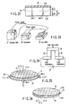
- FIGS. 5 to 9 sequentially show parts of a manufacturing process and parts of a manufacturing apparatus, for illustrating a semiconductor device manufacturing method and apparatus according to a first embodiment of the present invention.
- a dicing tape (protection member, protection tape or holding tape) 22 is affixed to an element forming surface 21 A side of a semiconductor wafer 21 on which elements have been formed.
- grooves (damage layers) 24 - 1 , 24 - 2 , 24 - 3 , . . . used as starting points to divide the semiconductor wafer into discrete semiconductor chips are formed on a rear surface 21 B side of the semiconductor wafer 21 which is opposite to the element forming surface 21 A by use of a diamond blade 23 .
- the grooves 24 - 1 , 24 - 2 , 24 - 3 , . . . are formed shallower than the thickness of the semiconductor chip obtained at the time of completion.
- a breaking process is performed to cleave the semiconductor wafer 21 by using the grooves 24 - 1 , 24 - 2 , 24 - 3 , . . . as the starting points to form discrete semiconductor chips 21 - 1 , 21 - 2 , 21 - 3 , . . . .
- a portion on the rear surface 21 B side of the discretely divided semiconductor wafer 21 is ground and removed until the semiconductor wafer comes to have preset thickness. If the depth of the grooves 24 - 1 , 24 - 2 , 24 - 3 , . . . is ⁇ 1 and the grinding amount is ⁇ 2, then damage layers such as scratches or distortions formed on the side surfaces of the semiconductor chips 21 - 1 , 21 - 2 , 21 - 3 , . . . by forming the grooves 24 - 1 , 24 - 2 , 24 - 3 , . . . can be removed by setting up the relation of ⁇ 1 ⁇ 2.
- ⁇ 2 becomes equal to 695 to 275 ⁇ m if the final thickness ⁇ 3 of the semiconductor chips 21 - 1 , 21 - 2 , 21 - 3 , . . . is 30 to 450 ⁇ m and therefore the depth ⁇ 1 of the grooves 24 - 1 , 24 - 2 , 24 - 3 , . . . can be freely and selectively set in a range shallower than 695 to 275 ⁇ m.
- the semiconductor chips 21 - 1 , 21 - 2 , 21 - 3 , . . . picked up by use of a picker are mounted on lead frames or TAB tapes and sealed into resin or ceramic packages, respectively, to complete semiconductor devices.
- the grooves 24 - 1 , 24 - 2 , 24 - 3 , . . . are formed in a region (discarding portion) which is to be removed in the back-side grinding process, the damage layers are not left behind on the semiconductor chips 21 - 1 , 21 - 2 , 21 - 3 , . . . obtained after the back-side grinding process and occurrence of distortion of Si and minute cracks of the separation surface and edge portion can be prevented.
- the side surface of the semiconductor chip sealed into the package is a cleavage plane, uneven portions and scratches are not formed on the element forming surface and side surface of the semiconductor chip and the quality and shape thereof are good as shown in FIGS. 10A and 10B.
- FIGS. 11 to 15 sequentially show parts of a manufacturing process and parts of a manufacturing apparatus, for illustrating a semiconductor device manufacturing method and apparatus according to a second embodiment of the present invention.
- a dicing tape (protection member, protection tape or holding tape) 22 is affixed to an element forming surface 21 A side of a semiconductor wafer 21 on which elements have been formed.
- scratches or distortions (damage layers) 28 - 1 , 28 - 2 , 28 - 3 , . . . used as starting points to divide the semiconductor wafer into discrete semiconductor chips are formed on a rear surface 21 B side of the semiconductor wafer 21 which is opposite to the element forming surface 21 A by use of a diamond scriber 27 .
- the scratches or distortions 28 - 1 , 28 - 2 , 28 - 3 , . . . are formed shallower than the thickness of the semiconductor chip obtained at the time of completion.
- a breaking process is performed to cleave the semiconductor wafer 21 by using the scratches or distortions 28 - 1 , 28 - 2 , 28 - 3 , . . . as the starting points to form discrete semiconductor chips 21 - 1 , 21 - 2 , 21 - 3 , . . . .
- a portion on the rear surface 21 B side of the discretely divided semiconductor wafer 21 is ground and removed until the semiconductor wafer comes to have preset thickness. If the depth of the scratches or distortions 28 - 1 , 28 - 2 , 28 - 3 , . . . is ⁇ 4 and the grinding amount is ⁇ 2 , then damage layers such as scratches or distortions formed on the side surfaces of the semiconductor chips 21 - 1 , 21 - 2 , 21 - 3 , . . . can be removed by setting up the relation of ⁇ 4 ⁇ 2 .
- ⁇ 2 becomes equal to 695 to 275 ⁇ m if the final thickness ⁇ 3 of the semiconductor chips 21 - 1 , 21 - 2 , 21 - 3 , . . . is 30 to 450 ⁇ m and therefore the depth ⁇ 4 of the scratches or distortions 28 - 1 , 28 - 2 , 28 - 3 , . . . can be freely and selectively set in a range shallower than 695 to 275 ⁇ m.
- the semiconductor chips 21 - 1 , 21 - 2 , 21 - 3 , . . . picked up by use of a picker are mounted on lead frames or TAB tapes and sealed into resin or ceramic packages, respectively, to complete semiconductor devices.
- the scratches or distortions 28 - 1 , 28 - 2 , 28 - 3 , . . . are formed in a region (discarding portion) which is to be removed in the back-side grinding process, damage layers are not left behind after the back-side grinding process and occurrence of distortion of Si and minute cracks of the separation surface and edge portion can be prevented. Further, since the side surface of the semiconductor chip sealed into the package is a cleavage plane, uneven portions and scratches are not formed on the element forming surface and side surface of the semiconductor chip and the quality and shape thereof are good.
- FIGS. 16 to 20 sequentially show parts of a manufacturing process and parts of a manufacturing apparatus, for illustrating a semiconductor device manufacturing method and apparatus according to a third embodiment of the present invention.
- a dicing tape (protection member, protection tape or holding tape) 22 is affixed to an element forming surface 21 A side of a semiconductor wafer 21 on which elements have been formed.
- Si re-crystallization layers (damage layers) 30 - 1 , 30 - 2 , 30 - 3 , . . . used as starting points to divide the semiconductor wafer into discrete semiconductor chips are formed on a rear surface 21 B side of the semiconductor wafer 21 which is opposite to the element forming surface 21 A by irradiating a laser beam from a laser irradiation device 29 .
- the re-crystallization layers 30 - 1 , 30 - 2 , 30 - 3 , . . . are formed shallower than the thickness of the semiconductor chip obtained at the time of completion.
- the re-crystallization layers 30 - 1 , 30 - 2 , 30 - 3 , . . . in a direction corresponding to the crystallization direction of the semiconductor wafer (for example, Si) since the re-crystallization layers are used as the starting points of cleavage.
- a breaking process is performed to cleave the semiconductor wafer 21 by using the re-crystallization layers 30 - 1 , 30 - 2 , 30 - 3 , . . . as the starting points to form discrete semiconductor chips 21 - 1 , 21 - 2 , 21 - 3 , . . . .
- a portion on the rear surface 21 B side of the discretely divided semiconductor wafer 21 is ground and removed until the semiconductor wafer comes to have preset thickness. If the depth of the re-crystallization.layers 30 - 1 , 30 - 2 , 30 - 3 , . . . is ⁇ 5 and the grinding amount is ⁇ 2 , then damage layers formed on the side surfaces of the semiconductor chips 21 - 1 , 21 - 2 , 21 - 3 , . . . by forming the re-crystallization layers 30 - 1 , 30 - 2 , 30 - 3 , . . . can be removed by setting up the relation of ⁇ 5 ⁇ 2 .
- ⁇ 2 becomes equal to 695 to 275 ⁇ m if the final thickness ⁇ 3 of the semiconductor chips 21 - 1 , 21 - 2 , 21 - 3 , . . . is 30 to 450 ⁇ m and therefore the depth ⁇ 5 of the re-crystallization layers 30 - 1 , 30 - 2 , 30 - 3 , . . . can be freely and selectively set in a range shallower than 695 to 275 ⁇ m.
- the semiconductor chips 21 - 1 , 21 - 2 , 21 - 3 , . . . picked up by use of a picker are mounted on lead frames or TAB tapes and sealed into resin or ceramic packages, respectively, to complete semiconductor devices.
- the Si re-crystallization layers 30 - 1 , 30 - 2 , 30 - 3 , . . . are formed in a region (discarding portion) which is to be removed in the back-side grinding process, damage layers are not left behind after the back-side grinding process and occurrence of distortion of Si and minute cracks of the separation surface and edge portion can be prevented. Further, since the side surface of the semiconductor chip sealed into the package is a cleavage plane, uneven portions and scratches are not formed on the element forming surface and side surface of the semiconductor chip and the quality and shape thereof are good.
- FIGS. 21 and 22 sequentially show parts of a manufacturing process and parts of a manufacturing apparatus, for illustrating a semiconductor device manufacturing method and apparatus according to a fourth embodiment of the present invention.
- silicon re-crystallization regions 30 A- 1 , 30 A- 2 , 30 A- 3 , . . . are formed in a semiconductor wafer 21 by focusing a laser beam on the internal portion of the semiconductor wafer 21 and adjusting laser beam power when the laser beam is applied.
- damage layers can be removed by setting up the relation of ⁇ 6 ⁇ 2 when the depth of the re-crystallization regions 30 A- 1 , 30 A- 2 , 30 A- 3 , . . . is ⁇ 6 and the grinding amount is ⁇ 2 .
- FIGS. 23 and 24 sequentially show parts of a manufacturing apparatus, for illustrating a semiconductor device manufacturing method and apparatus according to a fifth embodiment of the present invention.
- the silicon re-crystallization layers 30 - 1 , 30 - 2 , 30 - 3 , . . . or 30 A- 1 , 30 A- 2 , 30 A- 3 , . . . are formed in the semiconductor wafer 21 by irradiating the laser beam.
- laser processing gives a bad influence on the semiconductor chip by generation of heat.
- the semiconductor wafer 21 is held by use of an ice chuck shown in FIG. 23 and a laser beam is applied to the semiconductor wafer 21 while it is set in a cooled state.
- the ice chuck shown in FIG. 23 includes a cooling bath 31 , controller 32 and ice plate 33 .
- a refrigerant is supplied from the cooling bath 32 to the ice plate 33 to cool the same.
- the semiconductor wafer 21 is held on the ice plate 33 and cooled.
- the temperature of the ice plate 33 is controlled in a temperature range of approximately ⁇ 40° C. to 5° C. by the controller 32 .
- an influence of heat given to the semiconductor chip at the time of laser processing can be significantly reduced and occurrence of an operation failure of the semiconductor chip, for example, a degraded pause characteristic of a DRAM can be suppressed.
- the ice chuck is not limited to the configuration containing the cooling bath 31 as shown in FIG. 23 and can be provided with a thermoelectric cooling unit using a Peltier element as shown in FIG. 24 .
- the Peltier element includes a P-type element 34 , N-type element 35 and metal electrode 36 . Voltage is applied to the Peltier element from a power supply 37 to generate or absorb heat by causing a current to flow across the contact surface between the different types of metals.
- the ice chuck using the Peltier element makes it easy to control temperatures and cool an object to a set temperature in a short period of time.
- FIG. 25 is a perspective view showing part of a manufacturing process and a manufacturing apparatus, for illustrating a semiconductor device manufacturing method and apparatus according to a sixth embodiment of the present invention.
- the semiconductor wafer is divided by cleavage and breaking.
- a dicing tape 22 is stretched in directions indicated by arrows in the drawing by use of stretching jigs 38 - 1 , 38 - 2 , 38 - 3 , . . . to divide the semiconductor wafer by using grooves 24 - 1 , 24 - 2 , 24 - 3 , . . . , scratches or distortions 28 - 1 , 28 - 2 , 28 - 3 , . . . , re-crystallization layers 30 - 1 , 30 - 2 , 30 - 3 , . . . , or re-crystallization layers 30 A- 1 , 30 A- 2 , 30 A- 3 , . . . as starting points.
- the semiconductor wafer 21 can be divided into discrete semiconductor chips 21 - 1 , 21 - 2 , 21 - 3 , . . . by stretching the dicing tape 22 .
- FIG. 26 is a perspective view showing part of a manufacturing process, for illustrating a semiconductor device manufacturing method and apparatus according to a seventh embodiment of the present invention.
- the dicing tape 22 is affixed to the element forming surface 21 A of the semiconductor wafer 21 , but it is possible to affix a dicing tape 22 mounted on a wafer ring.
- the wafer ring can be used depending on the configuration of the manufacturing apparatus or the like.
- the rear surface portion of the semiconductor wafer can be removed only by etching if the amount of grinding of the rear surface portion is small.
- the dividing direction of the semiconductor wafer can be set in a direction perpendicular to the rear surface of the wafer or in the same direction as the Si crystallization direction.
- the damage layers such as the grooves 24 - 1 , 24 - 2 , 24 - 3 , . . . scratches or distortions 28 - 1 , 28 - 2 , 28 - 3 , . . . , re-crystallization layers 30 - 1 , 30 - 2 , 30 - 3 , . . . , or re-crystallization layers 30 A- 1 , 30 A- 2 , 30 A- 3 , . . . are formed while the dicing tape is kept affixed to the element forming surface side of the semiconductor wafer.
- the damage layers can be formed without using the dicing tape, a protection tape 22 is affixed to the element forming surface 21 A before the semiconductor wafer 21 is divided, and then the semiconductor wafer 21 can be divided by breaking and cleaving or by stretching the protection tape 22 .
- protection tape 22 is affixed to the element forming surface 21 A side of the semiconductor wafer 21 is explained as an example, but it is possible to affix a protection member other than the tape.
- adhesive resin is coated on the element forming surface 21 A side and a protection plate or holding plate can be affixed to the resin.
- a case wherein the pickup tape 26 is affixed and used instead of the dicing tape 22 , and the discrete semiconductor chips 21 - 1 , 21 - 2 , 21 - 3 , . . . are picked up is explained as an example. However, it is also possible to directly separate the semiconductor chips from the dicing tape 22 and pick up the semiconductor chips.
Landscapes
- Engineering & Computer Science (AREA)
- Mechanical Engineering (AREA)
- Physics & Mathematics (AREA)
- Optics & Photonics (AREA)
- Plasma & Fusion (AREA)
- Dicing (AREA)
- Mechanical Treatment Of Semiconductor (AREA)
Abstract
Description
Claims (26)
Priority Applications (1)
| Application Number | Priority Date | Filing Date | Title |
|---|---|---|---|
| US10/846,673 US20050023260A1 (en) | 2003-01-10 | 2004-05-17 | Semiconductor wafer dividing apparatus and semiconductor device manufacturing method |
Applications Claiming Priority (2)
| Application Number | Priority Date | Filing Date | Title |
|---|---|---|---|
| JP2003-004767 | 2003-01-10 | ||
| JP2003004767 | 2003-01-10 |
Related Child Applications (1)
| Application Number | Title | Priority Date | Filing Date |
|---|---|---|---|
| US10/846,673 Continuation-In-Part US20050023260A1 (en) | 2003-01-10 | 2004-05-17 | Semiconductor wafer dividing apparatus and semiconductor device manufacturing method |
Publications (1)
| Publication Number | Publication Date |
|---|---|
| US6756562B1 true US6756562B1 (en) | 2004-06-29 |
Family
ID=32501253
Family Applications (1)
| Application Number | Title | Priority Date | Filing Date |
|---|---|---|---|
| US10/390,900 Expired - Lifetime US6756562B1 (en) | 2003-01-10 | 2003-03-19 | Semiconductor wafer dividing apparatus and semiconductor device manufacturing method |
Country Status (3)
| Country | Link |
|---|---|
| US (1) | US6756562B1 (en) |
| DE (1) | DE10317115B4 (en) |
| TW (1) | TWI251874B (en) |
Cited By (15)
| Publication number | Priority date | Publication date | Assignee | Title |
|---|---|---|---|---|
| US20040224483A1 (en) * | 2003-02-28 | 2004-11-11 | Shinya Takyu | Semiconductor wafer dividing method and apparatus |
| US20050059325A1 (en) * | 2003-09-11 | 2005-03-17 | Yusuke Nagai | Wafer processing method |
| US20060030129A1 (en) * | 2004-08-05 | 2006-02-09 | Disco Corporation | Method and apparatus for dividing an adhesive film mounted on a wafer |
| US20060125060A1 (en) * | 2004-12-15 | 2006-06-15 | Elpida Memory Inc. | Semiconductor chip, and manufacturing method and application of the chip |
| US20060197260A1 (en) * | 2005-03-07 | 2006-09-07 | Disco Corporation | Laser processing method and laser beam processing machine |
| US7134943B2 (en) * | 2003-09-11 | 2006-11-14 | Disco Corporation | Wafer processing method |
| US20070066044A1 (en) * | 2005-06-01 | 2007-03-22 | Yoshiyuki Abe | Semiconductor manufacturing method |
| US20070085099A1 (en) * | 2003-09-10 | 2007-04-19 | Kenshi Fukumitsu | Semiconductor substrate cutting method |
| US20070105345A1 (en) * | 2005-11-09 | 2007-05-10 | Tetsuya Kurosawa | Semiconductor wafer dividing method |
| US20070138155A1 (en) * | 2005-12-21 | 2007-06-21 | Jenoptik Automatisierungstechnik Gmbh | Method and apparatus for severing disks of brittle material, in particular wafers |
| CN101941248A (en) * | 2009-07-07 | 2011-01-12 | 株式会社迪思科 | Topping machanism |
| US20110058585A1 (en) * | 2009-09-10 | 2011-03-10 | Sumitomo Electric Industries, Ltd. | Group-iii nitride semiconductor laser device, and method of fabricating group-iii nitride semiconductor laser device |
| DE102004025707B4 (en) * | 2003-05-26 | 2011-03-17 | Disco Corp. | Method of dividing a non-metallic substrate |
| US20110158275A1 (en) * | 2009-12-25 | 2011-06-30 | Sumitomo Electric Industries, Ltd. | Group-iii nitride semiconductor laser device, and method of fabricating group-iii nitride semiconductor laser device |
| US20110176569A1 (en) * | 2010-01-18 | 2011-07-21 | Sumitomo Electric Industries, Ltd. | Group-iii nitride semiconductor laser device, and method for fabricating group-iii nitride semiconductor laser device |
Families Citing this family (3)
| Publication number | Priority date | Publication date | Assignee | Title |
|---|---|---|---|---|
| JP4447392B2 (en) * | 2004-07-23 | 2010-04-07 | 株式会社ディスコ | Wafer dividing method and dividing apparatus |
| US7811904B2 (en) * | 2007-01-31 | 2010-10-12 | Alpha And Omega Semiconductor Incorporated | Method of fabricating a semiconductor device employing electroless plating |
| TWI657510B (en) * | 2014-10-02 | 2019-04-21 | 日商住友電木股份有限公司 | Method of manufacturing semiconductor device, and semiconductor device |
Citations (12)
| Publication number | Priority date | Publication date | Assignee | Title |
|---|---|---|---|---|
| US4224101A (en) | 1976-09-03 | 1980-09-23 | U.S. Philips Corporation | Method of manufacturing semiconductor devices using laser beam cutting |
| JPH0554262A (en) | 1991-08-28 | 1993-03-05 | Tokyo Electric Co Ltd | Product sales registration device |
| US5888883A (en) | 1997-07-23 | 1999-03-30 | Kabushiki Kaisha Toshiba | Method of dividing a wafer and method of manufacturing a semiconductor device |
| DE19811115A1 (en) | 1998-03-14 | 1999-09-16 | Stromberg Michael | Treating and processing wafers during thickness reduction and sawing |
| DE19840508A1 (en) | 1998-09-04 | 1999-12-02 | Siemens Ag | Separating individual semiconductor chips from composite wafer |
| EP1022778A1 (en) | 1999-01-22 | 2000-07-26 | Kabushiki Kaisha Toshiba | Method of dividing a wafer and method of manufacturing a semiconductor device |
| EP1026735A2 (en) | 1999-02-03 | 2000-08-09 | Kabushiki Kaisha Toshiba | Method of dividing a wafer and method of manufacturing a semiconductor device |
| US6184109B1 (en) | 1997-07-23 | 2001-02-06 | Kabushiki Kaisha Toshiba | Method of dividing a wafer and method of manufacturing a semiconductor device |
| US6294439B1 (en) | 1997-07-23 | 2001-09-25 | Kabushiki Kaisha Toshiba | Method of dividing a wafer and method of manufacturing a semiconductor device |
| US6337258B1 (en) * | 1999-07-22 | 2002-01-08 | Kabushiki Kaisha Toshiba | Method of dividing a wafer |
| JP2002192367A (en) | 2000-09-13 | 2002-07-10 | Hamamatsu Photonics Kk | Laser processing method |
| US6586707B2 (en) * | 2000-10-26 | 2003-07-01 | Xsil Technology Limited | Control of laser machining |
Family Cites Families (1)
| Publication number | Priority date | Publication date | Assignee | Title |
|---|---|---|---|---|
| JPS61112345A (en) * | 1984-11-07 | 1986-05-30 | Toshiba Corp | Manufacture of semiconductor device |
-
2003
- 2003-03-19 US US10/390,900 patent/US6756562B1/en not_active Expired - Lifetime
- 2003-04-14 DE DE10317115A patent/DE10317115B4/en not_active Expired - Fee Related
-
2004
- 2004-01-06 TW TW093100233A patent/TWI251874B/en not_active IP Right Cessation
Patent Citations (12)
| Publication number | Priority date | Publication date | Assignee | Title |
|---|---|---|---|---|
| US4224101A (en) | 1976-09-03 | 1980-09-23 | U.S. Philips Corporation | Method of manufacturing semiconductor devices using laser beam cutting |
| JPH0554262A (en) | 1991-08-28 | 1993-03-05 | Tokyo Electric Co Ltd | Product sales registration device |
| US5888883A (en) | 1997-07-23 | 1999-03-30 | Kabushiki Kaisha Toshiba | Method of dividing a wafer and method of manufacturing a semiconductor device |
| US6184109B1 (en) | 1997-07-23 | 2001-02-06 | Kabushiki Kaisha Toshiba | Method of dividing a wafer and method of manufacturing a semiconductor device |
| US6294439B1 (en) | 1997-07-23 | 2001-09-25 | Kabushiki Kaisha Toshiba | Method of dividing a wafer and method of manufacturing a semiconductor device |
| DE19811115A1 (en) | 1998-03-14 | 1999-09-16 | Stromberg Michael | Treating and processing wafers during thickness reduction and sawing |
| DE19840508A1 (en) | 1998-09-04 | 1999-12-02 | Siemens Ag | Separating individual semiconductor chips from composite wafer |
| EP1022778A1 (en) | 1999-01-22 | 2000-07-26 | Kabushiki Kaisha Toshiba | Method of dividing a wafer and method of manufacturing a semiconductor device |
| EP1026735A2 (en) | 1999-02-03 | 2000-08-09 | Kabushiki Kaisha Toshiba | Method of dividing a wafer and method of manufacturing a semiconductor device |
| US6337258B1 (en) * | 1999-07-22 | 2002-01-08 | Kabushiki Kaisha Toshiba | Method of dividing a wafer |
| JP2002192367A (en) | 2000-09-13 | 2002-07-10 | Hamamatsu Photonics Kk | Laser processing method |
| US6586707B2 (en) * | 2000-10-26 | 2003-07-01 | Xsil Technology Limited | Control of laser machining |
Non-Patent Citations (1)
| Title |
|---|
| Shinya Takyu et al., "Wafer Splitting Method Using Cleavage", Ser. No. 10/306,008, filed Nov. 29, 2002. |
Cited By (39)
| Publication number | Priority date | Publication date | Assignee | Title |
|---|---|---|---|---|
| US20040224483A1 (en) * | 2003-02-28 | 2004-11-11 | Shinya Takyu | Semiconductor wafer dividing method and apparatus |
| US7135384B2 (en) | 2003-02-28 | 2006-11-14 | Kabushiki Kaisha Toshiba | Semiconductor wafer dividing method and apparatus |
| DE102004025707B4 (en) * | 2003-05-26 | 2011-03-17 | Disco Corp. | Method of dividing a non-metallic substrate |
| US20100203678A1 (en) * | 2003-09-10 | 2010-08-12 | Hamamatsu Photonics K.K. | Semiconductor substrate cutting method |
| US8551817B2 (en) * | 2003-09-10 | 2013-10-08 | Hamamatsu Photonics K.K. | Semiconductor substrate cutting method |
| US8058103B2 (en) * | 2003-09-10 | 2011-11-15 | Hamamatsu Photonics K.K. | Semiconductor substrate cutting method |
| US20120077315A1 (en) * | 2003-09-10 | 2012-03-29 | Hamamatsu Photonics K.K. | Semiconductor substrate cutting method |
| US20070085099A1 (en) * | 2003-09-10 | 2007-04-19 | Kenshi Fukumitsu | Semiconductor substrate cutting method |
| DE102004043475B4 (en) * | 2003-09-11 | 2011-01-20 | Disco Corp. | Wafer processing method |
| US7134942B2 (en) * | 2003-09-11 | 2006-11-14 | Disco Corporation | Wafer processing method |
| US7134943B2 (en) * | 2003-09-11 | 2006-11-14 | Disco Corporation | Wafer processing method |
| US20050059325A1 (en) * | 2003-09-11 | 2005-03-17 | Yusuke Nagai | Wafer processing method |
| DE102004043474B4 (en) * | 2003-09-11 | 2011-07-07 | Disco Corp. | Wafer processing method |
| US20060030129A1 (en) * | 2004-08-05 | 2006-02-09 | Disco Corporation | Method and apparatus for dividing an adhesive film mounted on a wafer |
| CN100452287C (en) * | 2004-08-05 | 2009-01-14 | 株式会社迪斯科 | Method and device for breaking adhesive film mounted on wafer |
| US7602071B2 (en) | 2004-08-05 | 2009-10-13 | Disco Corporation | Apparatus for dividing an adhesive film mounted on a wafer |
| US7696609B2 (en) * | 2004-12-15 | 2010-04-13 | Elpida Memory, Inc. | Semiconductor device comprising a memory portion and a peripheral circuit portion |
| US20060125060A1 (en) * | 2004-12-15 | 2006-06-15 | Elpida Memory Inc. | Semiconductor chip, and manufacturing method and application of the chip |
| US20060197260A1 (en) * | 2005-03-07 | 2006-09-07 | Disco Corporation | Laser processing method and laser beam processing machine |
| US7737001B2 (en) | 2005-06-01 | 2010-06-15 | Renesas Technology Corp. | Semiconductor manufacturing method |
| US20070066044A1 (en) * | 2005-06-01 | 2007-03-22 | Yoshiyuki Abe | Semiconductor manufacturing method |
| US7642113B2 (en) | 2005-11-09 | 2010-01-05 | Kabushiki Kaisha Toshiba | Semiconductor wafer dividing method |
| US20070105345A1 (en) * | 2005-11-09 | 2007-05-10 | Tetsuya Kurosawa | Semiconductor wafer dividing method |
| US7816626B2 (en) * | 2005-12-21 | 2010-10-19 | Jenoptik Automatisierungstechnik Gmbh | Method and apparatus for severing disks of brittle material, in particular wafers |
| TWI485760B (en) * | 2005-12-21 | 2015-05-21 | 3D 麥可梅克公司 | Method and apparatus for cutting sheets, particularly wafers, from brittle materials |
| US20070138155A1 (en) * | 2005-12-21 | 2007-06-21 | Jenoptik Automatisierungstechnik Gmbh | Method and apparatus for severing disks of brittle material, in particular wafers |
| CN101941248B (en) * | 2009-07-07 | 2015-07-08 | 株式会社迪思科 | Cutting device |
| CN101941248A (en) * | 2009-07-07 | 2011-01-12 | 株式会社迪思科 | Topping machanism |
| US8227277B2 (en) * | 2009-09-10 | 2012-07-24 | Sumitomo Electric Industries, Ltd. | Group-III nitride semiconductor laser device, and method of fabricating group-III nitride semiconductor laser device |
| US20110058585A1 (en) * | 2009-09-10 | 2011-03-10 | Sumitomo Electric Industries, Ltd. | Group-iii nitride semiconductor laser device, and method of fabricating group-iii nitride semiconductor laser device |
| US20120088326A1 (en) * | 2009-09-10 | 2012-04-12 | Sumitomo Electric Industries, Ltd. | Group-iii nitride semiconductor laser device, and method of fabricating group-iii nitride semiconductor laser device |
| US8306082B2 (en) | 2009-09-10 | 2012-11-06 | Sumitomo Electric Industries, Ltd. | Group-III nitride semiconductor laser device, and method of fabricating group-III nitride semiconductor laser device |
| US8265113B2 (en) | 2009-12-25 | 2012-09-11 | Sumitomo Electric Industries, Ltd. | Group-III nitride semiconductor laser device, and method of fabricating group-III nitride semiconductor laser device |
| US20110158275A1 (en) * | 2009-12-25 | 2011-06-30 | Sumitomo Electric Industries, Ltd. | Group-iii nitride semiconductor laser device, and method of fabricating group-iii nitride semiconductor laser device |
| US8389312B2 (en) * | 2009-12-25 | 2013-03-05 | Sumitomo Electric Industries, Ltd. | Group-III nitride semiconductor laser device, and method of fabricating group-III nitride semiconductor laser device |
| US20120135554A1 (en) * | 2009-12-25 | 2012-05-31 | Sumitomo Electric Industries, Ltd. | Group-iii nitride semiconductor laser device, and method of fabricating group-iii nitride semiconductor laser device |
| US8213475B2 (en) | 2010-01-18 | 2012-07-03 | Sumitomo Electric Industries, Ltd. | Group-III nitride semiconductor laser device, and method for fabricating group-III nitride semiconductor laser device |
| US8071405B2 (en) | 2010-01-18 | 2011-12-06 | Sumitomo Electric Industries, Ltd. | Group-III nitride semiconductor laser device, and method for fabricating group-III nitride semiconductor laser device |
| US20110176569A1 (en) * | 2010-01-18 | 2011-07-21 | Sumitomo Electric Industries, Ltd. | Group-iii nitride semiconductor laser device, and method for fabricating group-iii nitride semiconductor laser device |
Also Published As
| Publication number | Publication date |
|---|---|
| TW200416852A (en) | 2004-09-01 |
| TWI251874B (en) | 2006-03-21 |
| DE10317115A1 (en) | 2004-07-22 |
| DE10317115B4 (en) | 2008-09-11 |
Similar Documents
| Publication | Publication Date | Title |
|---|---|---|
| US6756562B1 (en) | Semiconductor wafer dividing apparatus and semiconductor device manufacturing method | |
| US20050023260A1 (en) | Semiconductor wafer dividing apparatus and semiconductor device manufacturing method | |
| US7135384B2 (en) | Semiconductor wafer dividing method and apparatus | |
| JP4542789B2 (en) | Semiconductor device manufacturing apparatus and manufacturing method thereof | |
| US7172951B2 (en) | Apparatus for controlled fracture substrate singulation | |
| JP4840174B2 (en) | Manufacturing method of semiconductor chip | |
| US9601437B2 (en) | Plasma etching and stealth dicing laser process | |
| JP4840200B2 (en) | Manufacturing method of semiconductor chip | |
| US8969177B2 (en) | Laser and plasma etch wafer dicing with a double sided UV-curable adhesive film | |
| US9099546B2 (en) | Workpiece dividing method including two laser beam application steps | |
| CN100452287C (en) | Method and device for breaking adhesive film mounted on wafer | |
| US7579260B2 (en) | Method of dividing an adhesive film bonded to a wafer | |
| US8148240B2 (en) | Method of manufacturing semiconductor chips | |
| US7485547B2 (en) | Method of fabricating semiconductor device | |
| JP6713212B2 (en) | Method for manufacturing semiconductor device chip | |
| US9633903B2 (en) | Device manufacturing method of processing cut portions of semiconductor substrate using carbon dioxide particles | |
| CN101366113A (en) | Method for manufacturing semiconductor chip | |
| TW201725647A (en) | Equipment for plasma pelletizing | |
| WO2015087904A1 (en) | Wafer processing method | |
| JP2005109155A (en) | Semiconductor wafer processing method | |
| US11024542B2 (en) | Manufacturing method of device chip | |
| US12062533B2 (en) | Method of producing a substrate and system for producing a substrate | |
| US20190348290A1 (en) | Singulation of silicon carbide semiconductor wafers | |
| US10529623B2 (en) | Method of manufacturing light emitting element | |
| US12087630B2 (en) | Chip manufacturing method |
Legal Events
| Date | Code | Title | Description |
|---|---|---|---|
| AS | Assignment |
Owner name: KABUSHIKI KAISHA TOSHIBA, JAPAN Free format text: ASSIGNMENT OF ASSIGNORS INTEREST;ASSIGNORS:KUROSAWA, TETSUYA;TAKYU, SHINYA;SATO, NINAO;REEL/FRAME:014096/0151 Effective date: 20030512 |
|
| STCF | Information on status: patent grant |
Free format text: PATENTED CASE |
|
| FPAY | Fee payment |
Year of fee payment: 4 |
|
| FPAY | Fee payment |
Year of fee payment: 8 |
|
| FPAY | Fee payment |
Year of fee payment: 12 |
|
| AS | Assignment |
Owner name: TOSHIBA MEMORY CORPORATION, JAPAN Free format text: ASSIGNMENT OF ASSIGNORS INTEREST;ASSIGNOR:KABUSHIKI KAISHA TOSHIBA;REEL/FRAME:043709/0035 Effective date: 20170706 |
|
| AS | Assignment |
Owner name: K.K. PANGEA, JAPAN Free format text: MERGER;ASSIGNOR:TOSHIBA MEMORY CORPORATION;REEL/FRAME:055659/0471 Effective date: 20180801 Owner name: TOSHIBA MEMORY CORPORATION, JAPAN Free format text: CHANGE OF NAME AND ADDRESS;ASSIGNOR:K.K. PANGEA;REEL/FRAME:055669/0401 Effective date: 20180801 Owner name: KIOXIA CORPORATION, JAPAN Free format text: CHANGE OF NAME AND ADDRESS;ASSIGNOR:TOSHIBA MEMORY CORPORATION;REEL/FRAME:055669/0001 Effective date: 20191001 |