US6718476B1 - Method of synchronizing each local clock to a master clock in a data bus system - Google Patents
Method of synchronizing each local clock to a master clock in a data bus system Download PDFInfo
- Publication number
- US6718476B1 US6718476B1 US09/724,208 US72420800A US6718476B1 US 6718476 B1 US6718476 B1 US 6718476B1 US 72420800 A US72420800 A US 72420800A US 6718476 B1 US6718476 B1 US 6718476B1
- Authority
- US
- United States
- Prior art keywords
- node
- port
- local clock
- data bus
- clock
- Prior art date
- Legal status (The legal status is an assumption and is not a legal conclusion. Google has not performed a legal analysis and makes no representation as to the accuracy of the status listed.)
- Expired - Fee Related, expires
Links
Images


Classifications
-
- G—PHYSICS
- G06—COMPUTING; CALCULATING OR COUNTING
- G06F—ELECTRIC DIGITAL DATA PROCESSING
- G06F1/00—Details not covered by groups G06F3/00 - G06F13/00 and G06F21/00
- G06F1/04—Generating or distributing clock signals or signals derived directly therefrom
- G06F1/12—Synchronisation of different clock signals provided by a plurality of clock generators
-
- H—ELECTRICITY
- H04—ELECTRIC COMMUNICATION TECHNIQUE
- H04J—MULTIPLEX COMMUNICATION
- H04J3/00—Time-division multiplex systems
- H04J3/02—Details
- H04J3/06—Synchronising arrangements
- H04J3/0635—Clock or time synchronisation in a network
- H04J3/0679—Clock or time synchronisation in a network by determining clock distribution path in a network
-
- H—ELECTRICITY
- H04—ELECTRIC COMMUNICATION TECHNIQUE
- H04J—MULTIPLEX COMMUNICATION
- H04J3/00—Time-division multiplex systems
- H04J3/02—Details
- H04J3/06—Synchronising arrangements
- H04J3/0635—Clock or time synchronisation in a network
- H04J3/0685—Clock or time synchronisation in a node; Intranode synchronisation
- H04J3/0688—Change of the master or reference, e.g. take-over or failure of the master
Definitions
- the present invention generally relates to the field of data bus systems. More particularly, the present invention relates to the field of synchronizing local clocks in a data bus system.
- the 1394 Serial Bus Standard (or 1394 Standard) is a protocol for a high performance digital serial data bus.
- the 1394 Standard provides a versatile, high-speed method of interconnecting a variety of devices (e.g., computer system, digital camera, digital VCR, TV settop box, digital camcorder, storage device, digital audio device, etc.).
- the 1394 Standard enables a wide range of applications, including desktop video editing, publishing, data storage, video conferencing, and home Audio/Video networking. Rapid embrace of the 1394 Standard has been spurred by the emergence of digital video and multimedia applications.
- the 1394 Standard offers many advantages over other technologies.
- the major advantages include very high speed data transfer rates, self-configuring, plug-and-play operation, both asynchronous data transfer (guaranteed delivery) and isochronous data transfer (guaranteed bandwidth with low overhead), and flexible topology.
- the 1394 Standard was originally adopted in 1995 as the 1394-1995 specification. Later, the original specification was revised, providing some clarification on the original specification, changing some optional portions of the original specification to mandatory, and adding some performance enhancements. The first revision was approved and is known as the 1394a specification. A second revision of the 1394 Standard is known as the 1394b specification. The 1394b specification represents a significant enhancement of the 1394 Standard.
- FIG. 1 illustrates the well-known protocol layers of the 1394 Standard, whereas each device compliant with the 1394 Standard implements the protocol layers.
- the 1394 Standard includes a transaction layer 20 , a link layer 30 , a physical layer 40 , and a serial bus management layer 60 .
- the protocol layers interact and interface with the host 10 (e.g., processor, PCI Bus, application, etc.) and with the 1394 connector, whereas the 1394 connector physically couples one device to another device.
- Each protocol layer is implemented as circuitry, software, or both.
- the physical layer 40 is responsible for the clocking scheme of the 1394 Standard.
- the physical layer 40 maintains a local clock, whereas each device has a respective local clock.
- Data transmissions from a transmitting device to a receiving device are synchronized by the local clock of the transmitting device.
- the transmitting device transmits data and its local clock to the receiving device.
- the receiving device recovers the local clock of the transmitting device and utilizes the recovered local clock to recover the data transmitted by the transmitting device.
- FIG. 2 illustrates a conventional 1394b data bus system 200 according to the prior art, showing the conventional clocking scheme of the prior art.
- the conventional 1394b data bus system 200 includes a plurality of nodes 210 A- 210 F.
- Each node is a device (e.g., computer system, digital camera, digital VCR, TV settop box, digital camcorder, storage device, digital audio device, etc.) which is compliant with the 1394b specification.
- One of the plurality of nodes is designated as a root node according to the 1394b specification.
- node A 210 A is the root node 210 A.
- Each node 210 A- 210 F includes an oscillator 215 A- 215 F for generating a respective local clock 220 A- 220 F or CLK A-CLK F, whereas each local clock 220 A- 220 F operates at a nominal frequency of 25 MHz.
- each node 210 A- 210 F includes a cycle counter 230 A- 230 F for coordinating time dependent data (e.g., digital video data, digital audio data, etc.). Each cycle counter 230 A- 230 F is incremented by a respective local clock 220 A- 220 F.
- each node 210 A- 210 F includes a buffer 240 A- 240 F for storing data which is to be transmitted to another node or which has been received from another node.
- Node A 210 A includes a port 262 A coupled to a phase locked loop 252 A, a port 264 A coupled to a phase locked loop 254 A, and a port 266 A coupled to a phase locked loop 256 A.
- Node B 210 B includes a port 262 B coupled to a phase locked loop 252 B and a port 264 B coupled to a phase locked loop 254 B.
- Node C 210 C includes a port 262 C coupled to a phase locked loop 252 C.
- Node D 210 D includes a port 262 D coupled to a phase locked loop 252 D.
- Node E 210 E includes a port 262 E coupled to a phase locked loop 252 E and a port 264 E coupled to a phase locked loop 254 E.
- Node F 210 F includes a port 262 F coupled to a phase locked loop 252 F.
- each node 210 A- 210 F assigns a parent port identifier (illustrated by “P”) to a port to indicate that a node which is closer to the root node 210 A is coupled to that port. Moreover, each node 210 A- 210 F assigns a child port identifier (illustrated by “C”) to a port to indicate that a node which is farther away from the root node 210 A is coupled to that port.
- the port 262 B of node B 210 B is a parent port because port 262 B is coupled to node A 210 A, which is a node that is actually the root node 210 A.
- the port 262 C of node C 210 C is a parent port because port 262 C is coupled to node B 210 B, which is a node that is closer to the root node 210 A.
- the port 262 A of node A 210 A (the root node) is a child port because port 262 A is coupled to node B 210 B, which is a node that is farther from the root node 210 A.
- the port 264 B of node B 210 B is a child port because port 264 B is coupled to node C 210 C, which is a node that is farther from the root node 210 A.
- Node A 210 A transmits data via data connections 271 , 276 , and 278 .
- Node B 210 B transmits data via data connections 272 and 273 .
- Node C 210 C transmits data via data connection 274 .
- Node D 210 D transmits data via data connection 275 .
- Node E 210 E transmits data via data connections 277 and 270 .
- Node F 210 F transmits data via data connection 279 .
- Each data connection 270 - 279 is a twisted wire pair.
- a transmitting node uses its local clock (e.g., CLK A) to synchronize transmission of data packets to the receiving node (e.g., node B 210 B) via a data connection (e.g., data connection 271 ).
- the transmitting node e.g., node A 210 A
- encodes on a single twisted wire pair e.g., data connection 271
- the data packets and its local clock e.g., CLK A
- the receiving node (e.g., node B 210 B) utilizes a phase locked loop (e.g., phase locked loop 252 B) (which is coupled to the port that is coupled to the transmitting node) to recover the local clock (e.g., CLK A) of the transmitting node (e.g., node A 210 A).
- the receiving node (e.g., node B 210 B) utilizes the recovered local clock (e.g., CLK A) to recover the data packets transmitted via a data connection (e.g., data connection 271 ).
- the receiving node e.g., node B 210 B
- the receiving/retransmitting node uses its local clock (e.g., CLK B) to synchronize transmission of data packets to a second receiving node (e.g., node C 210 C) via a data connection (e.g., data connection 273 ).
- CLK B local clock
- the receiving/retransmitting node encodes on a single twisted wire pair (e.g., data connection 273 ) the data packets and its local clock (e.g., CLK B).using a 8 B 10 B coding.
- the second receiving node e.g., node C 210 C
- utilizes a phase locked loop e.g., phase locked loop 252 C
- the local clock e.g., CLK B
- the second receiving node utilizes the recovered local clock (e.g., CLK B) to recover the data packets transmitted via a data connection (e.g., data connection 273 ).
- a cycle master which is typically the root node 210 A synchronizes the cycle counters 230 B- 230 F of the other nodes 210 B- 210 F to the cycle counter 230 A of the cycle master (the root node 210 A).
- the root node 210 A transmits a cycle start packet every 125 microseconds (or at the start of an isochronous cycle) to the receiving nodes (node B 210 B, node D 210 D and node E 210 E) via data connections 271 , 276 , and 278 .
- the cycle start packet is transmitted as described above.
- the cycle start packet includes the value of the cycle counter 230 A of the root node 210 A.
- the receiving nodes (node B 210 B, node D 210 D and node E 210 E) copy the value of the cycle counter 230 A of the root node 210 A to their respective cycle counter 230 B, 230 D, and 230 E. Moreover, the receiving nodes (node B 210 B and node E 210 E) retransmit the cycle start packet to node C 210 C and node F 210 F, respectively, so that node C 210 C and node F 210 F are able to copy the value of the cycle counter 230 A of the root node 210 A to their respective cycle counter 230 C and 230 F.
- the cycle start packet is synchronized to the local clock at each intermediate node prior to retransmission, a propagation time is introduced to the cycle start packet.
- This propagation time is a source of jitter in the respective cycle counters of the nodes.
- the respective cycle counters 230 B- 230 F (which are incremented by respective local clocks CLK B-CLK F) can lead or lag the cycle counter 230 A of the root node 210 A prior to receiving the cycle start packet. This translates directly to jitter in the respective cycle counters 230 B- 230 F, causing distortion in any data processing operation that uses the respective cycle counter 230 B- 230 F as a time reference.
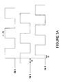
- FIGS. 3A-3D illustrate the relationship over a period of time between the local clocks of the nodes of the conventional 1394b data bus system of FIG. 2, showing the source of jitter in the respective cycle counter of the nodes.
- each local clock operates at a nominal frequency of 25 MHz.
- CLK A is the local clock of the root node 210 A
- the cycle counter 230 A of the root node 210 A is incremented by CLK A.
- the root node 210 A synchronizes the cycle counters 230 B- 230 F of the other nodes 210 B- 210 F to its cycle counter 230 A by transmitting a cycle start packet that has the value of the cycle counter 230 A of the root node 210 A.
- CLK B is the local clock of node B 210 B.
- CLK C is the local clock of node C 210 C.
- FIGS. 3A-3D illustrate that the phase of CLK B with respect to CLK A drifts over time. Moreover, FIGS. 3A-3D illustrate that the phase of CLK C with respect to CLK A drifts over time.
- the data bus system includes a plurality of nodes each having a local clock, whereas the data bus system is compliant with the 1394b specification.
- each node includes a local clock generator, one or more ports, and one or more clock recovery circuits each coupled to a respective port.
- a clock source for each local clock is the respective local clock generator of each node.
- each node assigns either a first identifier or a second identifier to each port that is coupled to another port.
- the first identifier is a parent port and the second identifier is a child port. If a node has a first identifier port, the node changes a clock source for its local clock from the local clock generator to a particular clock recovery circuit that is coupled to the first identifier port.
- the particular clock recovery circuit recovers a transmitted local clock of a transmitting node that is coupled to the first identifier port, whereas the transmitting node has a second identifier port which couples to the first, identifier port.
- the plurality of nodes includes a root node, whereas the root node does not have a first identifier port and has at least one second identifier port for transmitting its local clock to another node.
- the local clock of the root node serves as the master clock for synchronizing the local clocks of the other nodes, reducing jitter in the cycle counters of the nodes when the cycle counters are updated with the value of the cycle counter of the root node.
- the data bus system includes a plurality of nodes each having a local clock, whereas the data bus system is compliant with the 1394b specification.
- each node includes one or more ports and a multiple mode clock recovery circuit, whereas the multiple mode clock recovery circuit operates in each of a plurality of modes including a locked mode and an unlocked mode.
- a clock source for each local clock is the respective multiple mode clock recovery circuit (of each node) operating in the unlocked mode.
- each node assigns either a first identifier or a second identifier to each port that is coupled to another port.
- the first identifier is a parent port and the second identifier is a child port. If a node has a first identifier port, the node changes a clock source for its local clock from the multiple mode clock recovery circuit operating in the unlocked mode to the multiple mode clock recovery circuit operating in the locked mode.
- the multiple mode clock recovery circuit operating in the locked mode recovers a transmitted local clock of a transmitting node that is coupled to the first identifier port, whereas the transmitting node has a second identifier port which couples to the first identifier port.
- the plurality of nodes includes a root node, whereas the root node does not have a first identifier port and has at least one second identifier port for transmitting its local clock to another node.
- the local clock of the root node serves as the master clock for synchronizing the local clocks of the other nodes, reducing jitter in the cycle counters of the nodes when the cycle counters are updated with the value of the cycle counter of the root node.
- the present invention includes a method of synchronizing a plurality of local clocks in a data bus system having a plurality of nodes, each node having one of the plurality of local clocks, the method comprising the steps of: a) initiating formation of a data bus configuration for the data bus system, wherein each node includes a local clock generator, at least one port, and at least one clock recovery circuit coupled to a respective port, wherein a coupled port represents a port coupled to another port; b) for each node, assigning each coupled port one of a plurality of identifiers based on predetermined criteria the identifiers including a first identifier and a second identifier; and c) for each node which has a first identifier port, changing a clock source for a respective local clock of the node from a respective local clock generator of the node to a particular clock recovery circuit of the node, wherein the particular clock recovery circuit recovers a transmitted local clock of a transmitting node coupled to the first
- the present invention includes a method of synchronizing a plurality of local clocks in a data bus system having a plurality of nodes, each node having one of the plurality of local clocks, the method comprising the steps of: a) initiating formation of a data bus configuration for the data bus system, wherein each node includes at least one port and a multiple mode clock recovery circuit (MMCRC), wherein the MMCRC operates in each of a plurality of modes the modes including a locked mode and an unlocked mode, wherein a coupled port represents a port coupled to another port; b) for each node, assigning each coupled port one of a plurality of identifiers based on predetermined criteria the identifiers including a first identifier and a second identifier; and c) for each node which has a first identifier port, changing a clock source for a respective local clock of the node from the MMCRC operating in the unlocked mode to the MMCRC operating in the locked mode, wherein the MMC
- FIG. 1 illustrates the well-known protocol layers of the 1394 Standard, whereas each device compliant with the 1394 Standard implements the protocol layers.
- FIG. 2 illustrates a conventional 1394b data bus system 200 according to the prior art, showing the conventional clocking scheme of the prior art.
- FIGS. 3A, 3 B, 3 C, and 3 D illustrate the relationship over time between the local clocks of the nodes of the conventional 1394b data bus system of FIG. 2, showing the source of jitter in the respective cycle counter of the nodes.
- FIG. 4A illustrates a node according to an embodiment of the present invention, showing a local clock and one port.
- FIG. 4B illustrates a node according to an embodiment of the present invention, showing a local clock and multiple ports.
- FIG. 4C illustrates a phase locked loop according to an embodiment of the present invention.
- FIG. 5A illustrates a node according to an embodiment of the present invention, showing a local clock before clock synchronization.
- FIG. 5B illustrates a node according to an embodiment of the present invention, showing a local clock after clock synchronization.
- FIG. 6A illustrates a node according to an embodiment of the present invention, showing a local clock before clock synchronization.
- FIG. 6B illustrates a node according to an embodiment of the present invention, showing a local clock after clock synchronization.
- FIG. 7A illustrates a node according to an embodiment of the present invention, showing a local clock before clock synchronization.
- FIG. 7B illustrates a root node according to an embodiment of the present invention, showing a local clock after clock synchronization.
- FIG. 8 illustrates a 1394b data bus system according to an embodiment of the present invention, showing a clocking scheme according to the present invention.
- FIG. 8B illustrates the relationship between the local clocks of the nodes of the 1394b data bus system of FIG. 8, showing a fixed offset between the local clocks.
- FIG. 8C illustrates a flow diagram, showing a method of synchronizing local clocks in a data bus system in accordance with an embodiment of the present invention.
- FIG. 9A illustrates a node according to a second embodiment of the present invention, showing a local clock and one port.
- FIG. 9B illustrates a node according to a second embodiment of the present invention, showing a local clock and multiple ports.
- FIG. 9C illustrates a phase locked loop according to a second embodiment of the present invention.
- FIG. 10A illustrates a node according to a second embodiment of the present invention, showing a local clock before clock synchronization.
- FIG. 10B illustrates a node according to a second embodiment of the present invention, showing a local clock after clock synchronization.
- FIG. 11A illustrates a node according to a second embodiment of the present invention, showing a local clock before clock synchronization.
- FIG. 11B illustrates a node according to a second embodiment of the present invention, showing a local clock after clock synchronization.
- FIG. 12A illustrates a node according to a second embodiment of the present invention, showing a local clock before clock synchronization.
- FIG. 12B illustrates a root node according to a second embodiment of the present invention, showing a local clock after clock synchronization.
- FIG. 13 illustrates a 1394b data bus system according to a second embodiment of the present invention, showing a clocking scheme according to the present invention.
- FIG. 13B illustrates a flow diagram, showing a method of synchronizing local clocks in a data bus system in accordance with a second embodiment of the present invention.
- Each node is a device (e.g., computer system, digital camera, digital VCR, TV settop box, digital camcorder, storage device, digital audio device, etc.) which is compliant with the 1394b specification.
- a device e.g., computer system, digital camera, digital VCR, TV settop box, digital camcorder, storage device, digital audio device, etc.
- FIG. 4A illustrates a node 400 according to an embodiment of the present invention, showing a local clock CLK and one port.
- the node 400 is compliant with the 1394b specification.
- a plurality of nodes are coupled together to form a 1394b data bus system according an embodiment of the present invention.
- the 1394 Standard (including the 1394-1995 specification, the 1394a specification, and the 1394b specification) is comprised of a transaction layer, a link layer, a physical layer, and a serial bus management layer, whereas each protocol layer is implemented as circuitry, software, or both.
- the local clock CLK is implemented in the physical layer of the 1394b specification.
- the node 400 includes a local clock generator 415 , a port 460 , and a clock recovery circuit 450 coupled to the port 460 .
- the node 400 includes a buffer 440 and a cycle counter 430 .
- the port 460 facilitates coupling the node 400 to another port of another node. It should be understood that the node 400 can have more than one port, whereas each port is coupled to a separate clock recovery circuit.
- the clock recovery circuit 450 recovers a local clock that is transmitted by a transmitting node, that is coupled to the port 460 .
- the transmitting node encodes data packets together with its local clock using a 8 B 10 B coding prior to transmitting the data packets and its local clock.
- the recovered local clock can operate as the clock source for the local clock CLK of the node 400 .
- the clock recovery circuit 450 comprises a phase locked loop 450 . It should be understood that the clock recovery circuit 450 can be implemented in any other manner.
- the local clock generator 415 comprises a crystal oscillator 415 .
- the local clock generator 415 generates a signal which can operate as the clock source for the local clock CLK of the node 400 . It should be understood that the local clock generator 415 can be implemented in any other manner.
- the cycle counter 430 facilitates coordinating time dependent data (e.g., digital video data, digital audio data, etc.), as described above.
- the cycle counter 430 is incremented by the local clock CLK.
- the buffer 440 enables storing data which is to be transmitted to another node or which has been received from another node.
- the node 400 has a clock source selection circuit 490 .
- the clock source selection circuit 490 is coupled to an output terminal 457 of the clock recovery circuit 450 and is coupled to an output terminal 417 of the local clock generator 415 .
- the clock source selection circuit 490 has an output terminal 420 , whereas the output terminal 420 provides the local clock CLK for the node 400 .
- the node 400 selectively couples the output terminal 420 of the clock source selection circuit 490 to either the clock recovery circuit 450 or the local clock generator 415 , facilitating synchronization of the local clock CLK to a master clock so that to reduce jitter in the cycle counter 430 of the node 400 and in the cycle counters of the other nodes when the cycle counters are updated with the value of the cycle counter of the root node.
- the clock source selection circuit 490 comprises a switch 490 . It should be understood that the clock source selection circuit 490 can be implemented in any other manner. It should be understood that the clock source for the local clock CLK can be changed using an implementation other than the clock source selection circuit 490 .
- the node 400 operates with the local clock CLK coupled to the output terminal 417 of the local clock generator 415 via the clock source selection circuit 490 .
- the node 400 participates in establishing a data bus configuration for the 1394b data bus system.
- One of the nodes in the 1394b data bus system is designated the root node.
- the node 400 as well as the other nodes in the 1394b data bus system assign either a first identifier or a second identifier to their respective ports that are coupled to another port.
- the first identifier is a parent port and the second identifier is a child port.
- the parent port identifier is assigned to a port to indicate that a node which is closer to the root node is coupled to that port. Moreover, a child port identifier is assigned to a port to indicate that a node which is farther away from the root node is coupled to that port.
- the node 400 changes the clock source for its local clock CLK via the clock source selection circuit 490 .
- the clock source selection circuit 490 couples the output terminal 457 of the clock recovery circuit 450 to the local clock CLK of the node 400 rather than coupling the output terminal 417 of the local clock generator 415 to the local clock CLK of the node 400 , whereas the clock recovery circuit 450 recovers the local clock of the transmitting node coupled to the port 460 (the parent port) of the node 400 .
- the recovered local clock operates as the clock source for the local clock CLK of the node 400 , enabling synchronization of the local clock CLK of the node 400 and of the local clocks of the other nodes.
- the root node assigns a child port identifier to its port or ports, maintaining its local clock coupled to the output terminal of its local clock generator via its clock source selection circuit.
- the root node is coupled to at least one parent port of another node and transmits its local clock via its child port to the parent port of another node. Therefore, the local clock of the root node serves as the master clock for synchronizing the local clocks of the other nodes, reducing jitter in the cycle counters of the nodes when the cycle counters are updated with the value of the cycle counter of the root node.
- FIG. 4B illustrates a node 400 A according to an embodiment of the present invention, showing a local clock CLK and multiple ports 460 A and 461 A.
- the node 400 A includes a first port 460 A, a second port 461 A, a buffer 440 A, a cycle counter 430 A, a first clock recovery circuit 450 A coupled to the first port 460 A, a second clock recovery circuit 451 A coupled to the second port 461 A, and a local clock generator 415 A.
- the description of these elements with respect to node 400 in FIG. 4A is applicable to node 400 A in FIG. 4 B.
- node 400 A includes a clock source selection circuit 490 A.
- the clock source selection circuit 490 A is coupled to an output terminal 457 A of the first clock recovery circuit 450 A, an output terminal 458 A of the second clock recovery circuit 451 A, and an output terminal 417 A of the local clock generator 415 A.
- the clock source selection circuit 490 A has an output terminal 420 A, whereas the output terminal 420 A provides the local clock CLK for the node 400 A.
- the node 400 A selectively couples the output terminal 420 A of the clock source selection circuit 490 A to the first clock recovery circuit 450 A, the second clock recovery circuit 451 A, or the local clock generator 415 A.
- the node can selectively couple the output terminal of the clock source selection circuit to any of the clock recovery circuits of the node and to the local clock generator of the node.
- the discussion of the operation and synchronization of the local clock with respect to node 400 of FIG. 4A is applicable to node 400 A of FIG. 4 B.
- FIG. 4C illustrates a phase locked loop 450 according to an embodiment of the present invention.
- the phase locked loop 450 (or clock recovery circuit 450 ) of FIG. 4 A and the phase locked loops 450 A and 451 A (first clock recovery circuit 450 A and the second clock recovery circuit 451 A) of FIG. 4B can be configured as illustrated in FIG. 4 C.
- the phase locked loop 450 includes an input terminal 459 coupled to a port (not shown), a phase detector 401 coupled to the input terminal 459 , a low pass filter 403 coupled to the phase detector 401 , a voltage controlled oscillator 407 coupled to the low pass filter 403 and to the phase detector 401 , and an output terminal 457 coupled to the voltage controlled oscillator 407 .
- the voltage controlled oscillator 407 is replaced by a voltage controlled crystal oscillator.
- the phase locked loop 450 recovers a local clock transmitted via the port coupled to the input terminal 459 , as discussed above.
- the recovered local clock is outputted via the output terminal 457 , thus capable of operating as the clock source for the local clock of a node.
- the phase locked loop 450 can be implemented in any other manner and can have other components.
- FIG. 5A illustrates a node 400 A in a 1394b data bus system according to an embodiment of the present invention, showing a local clock CLK before clock synchronization.
- the local clock CLK is implemented in the physical layer of the 1394b specification.
- the node 400 A of FIG. 4B is illustrated in FIG. 5 A.
- the node 400 A is coupled to a first node (not shown) via port 460 A and is coupled to a second node (not shown) via port 461 A, whereas node 400 A transmits data and its local clock CLK via data connections 464 A and 466 A.
- Node 400 A receives data and the local clock of the first node via data connection 465 A.
- Node 400 A receives data and the local clock of the second node via data connection 467 A. Moreover, since the node 400 A has not assigned either a first identifier or a second identifier to its ports 460 A and 461 A, a data bus configuration for the 1394b data bus has not been established. In an embodiment, formation of the data bus configuration is initiated upon the occurrence of any event or condition specified in the 1394b specification (e.g., adding a node to the 1394b data bus system, removing a node from the 1394b data bus system, etc.). In an embodiment of the present invention, formation of the data bus configuration begins by performing a Bus Reset procedure as specified in the 1394b specification.
- FIG. 5A illustrates the node 400 A before its local clock CLK is synchronized to a master clock according to an embodiment of the present invention, whereas the master clock is the local clock of the root node as described above.
- the local clock CLK is provided by the local clock generator 415 A, whereas the clock source selection circuit 490 A couples the output terminal 417 A of the local clock generator 415 A to the output terminal 420 A of the clock source selection circuit 490 A.
- FIG. 5B illustrates a node 400 A in a 1394b data bus system according to an embodiment of the present invention, showing a local clock CLK after clock synchronization.
- the node 400 A participates in establishing the data bus configuration for the 1394b data bus system.
- one of the nodes is designated as the root node as specified in the 1394b specification.
- the node 400 A assigns a parent port identifier (illustrated by “P”) to port 460 A to indicate that a node which is closer to the root node is coupled to that port 460 A.
- P parent port identifier
- the node 400 A assigns a child port identifier (illustrated by “C”) to port 461 A to indicate that a node which is farther away from the root node is coupled to that port 461 A.
- the parent port of one node couples to the child port of another node.
- the other nodes in the 1394b data bus system perform a similar operation.
- the node 400 A assigns the particular identifier to its ports 460 A and 461 A during a Tree Identification procedure as specified in the 1394b specification.
- the node 400 A Since the node 400 A has a port 460 A that is assigned the parent port identifier, the node 400 A synchronizes its local clock CLK by changing a clock source for its local clock CLK. If the node 400 A does not have a port that is assigned the parent port identifier, the node 400 A would continue to have the local clock generator 415 A serve as the clock source for its local clock CLK.
- the root node is the node that does not have a port that is assigned the parent port identifier.
- the clock source selection circuit 490 A (of node 400 A) couples its output terminal 420 A to the output terminal 457 A of the first clock recovery circuit 450 A (which is coupled to port 460 A which is assigned the parent port identifier) instead of the output terminal 417 A of the local clock generator 415 A.
- the first clock recovery circuit 450 A recovers the local clock transmitted via data connection 465 A by the first node coupled to the port 460 A.
- the recovered local clock serves as the clock source for the local clock CLK of the node 400 A.
- the node 400 A utilizes the local clock CLK (which is the recovered local clock of the first node) to increment the cycle counter 430 A.
- the node 400 A utilizes the local clock CLK (which is the recovered local clock of the first node) to synchronize the transmission of data and its local clock CLK via data connections 464 A and 466 A during data transfer operations supported by the 1394b data bus system, whereas the node 400 A encodes the data together with its local clock CLK using a 8 B 10 B coding prior to transmitting the data and its local clock CLK.
- the node 400 A utilizes the local clock CLK (which is the recovered local clock of the first node) to perform any other operation requiring the use of its local clock CLK.
- the other nodes in the 1394b data bus system perform a similar operation.
- the node 400 A changes a clock source for its local clock CLK during a Self Identification procedure as specified in the 1394b specification.
- the node 400 A turns off or disables its local clock generator 415 A.
- the root node maintains its local clock generator as the clock source for its local clock, transmitting its local clock via its port or ports (which are assigned the child port identifier) to at least one port (of the other nodes) that is assigned the parent port identifier.
- the other nodes (including node 400 A) change the clock source for their local clocks such that a recovered local clock (which is outputted by a clock recovery circuit coupled to a port that is assigned the parent port identifier) serves as the clock source for the local clock of the other nodes (including node 400 A). Therefore, the local clock of the root node serves as the master clock for synchronizing the local clocks of the other nodes, reducing jitter in the cycle counters of the nodes when the cycle counters are updated with the value of the cycle counter of the root node.
- FIG. 6A illustrates a node 400 A in a 1394b data bus system according to an embodiment of the present invention, showing a local clock CLK before clock synchronization.
- the local clock CLK is implemented in the physical layer of the 1394b specification.
- the node 400 A of FIG. 4B is illustrated in FIG. 6 A.
- the node 400 A is coupled to a first node (not shown) via port 461 A, whereas node 400 A transmits data and its local clock CLK via data connection 462 A.
- Node 400 A receives data and the local clock of the first node via data connection 463 A.
- a data bus configuration for the 1394b data bus has not been established.
- formation of the data bus configuration is initiated upon the occurrence of any event or condition specified in the 1394b specification (e.g., adding a node to the 1394b data bus system, removing a node from the 1394b data bus system, etc.).
- formation of the data bus configuration begins by performing a Bus Reset procedure as specified in the 1394b specification.
- FIG. 6A illustrates the node 400 A before its local clock CLK is synchronized to a master clock according to an embodiment of the present invention, whereas the master clock is the local clock of the root node as described above.
- the local clock CLK is provided by the local clock generator 415 A, whereas the clock source selection circuit 490 A couples the output terminal 417 A of the local clock generator 415 A to the output terminal 420 A of the clock source selection circuit 490 A.
- FIG. 6B illustrates a node 400 A in a 1394b data bus system according to an embodiment of the present invention, showing a local clock CLK after clock synchronization.
- the node 400 A participates in establishing the data bus configuration for the 1394b data bus system.
- one of the nodes is designated as the root node as specified in the 1394b specification.
- the node 400 A assigns a parent port identifier (illustrated by “P”) to port 461 A to indicate that a node which is closer to the root node is coupled to that port 461 A.
- the parent port of one node couples to the child port of another node.
- node 400 A Since port 460 A is not coupled to another node, node 400 A does not assign a particular identifier to port 460 A.
- the other nodes in the 1394b data bus system perform a similar operation.
- the node 400 A assigns the particular identifier to its port 461 A during a Tree Identification procedure as specified in the 1394b specification.
- the node 400 A Since the node 400 A has a port 461 A that is assigned the parent port identifier, the node 400 A synchronizes its local clock CLK by changing a clock source for its local clock CLK.
- the clock source selection circuit 490 A (of node 400 A) couples its output terminal 420 A to the output terminal 458 A of the second clock recovery circuit 451 A (which is coupled to port 461 A which is assigned the parent port identifier) instead of the output terminal 417 A of the local clock generator 415 A.
- the second clock recovery circuit 451 A recovers the local clock transmitted via data connection 463 A by the first node coupled to the port 461 A.
- the recovered local clock serves as the clock source for the local clock CLK of the node 400 A.
- the node 400 A utilizes the local clock CLK (which is the recovered local clock of the first node) to increment the cycle counter 430 A. Moreover, the node 400 A utilizes the local clock CLK (which is the recovered local clock of the first node) to synchronize the transmission of data and its local clock CLK via data connection 462 A during data transfer operations supported by the 1394b data bus system, whereas the node 400 A encodes the data together with its local clock CLK using a 8 B 10 B coding prior to transmitting the data and its local clock CLK. In addition, the node 400 A utilizes the local clock CLK (which is the recovered local clock of the first node) to perform any other operation requiring the use of its local clock CLK.
- the other nodes in the 1394b data bus system perform a similar operation.
- the node 400 A changes a clock source for its local clock CLK during a Self Identification procedure as specified in the 1394b specification.
- the node 400 A turns off or disables its local clock generator 415 A.
- FIG. 7A illustrates a node 400 A in a 1394b data bus system according to an embodiment of the present invention, showing a local clock CLK before clock synchronization.
- the local clock CLK is implemented in the physical layer of the 1394b specification.
- the node 400 A of FIG. 4B is illustrated in FIG. 7 A.
- the node 400 A is coupled to a first node (not shown) via port 460 A and is coupled to a second node (not shown) via port 461 A, whereas node 400 A transmits data and its local clock CLK via data connections 464 A and 466 A.
- Node 400 A receives data and the local clock of the first node via data connection 465 A.
- Node 400 A receives data and the local clock of the second node via data connection 467 A. Moreover, since the node 400 A has not assigned either a first identifier or a second identifier to its ports 460 A and 461 A, a data bus configuration for the 1394b data bus has not been established. In an embodiment, formation of the data bus configuration is initiated upon the occurrence of any event or condition specified in the 1394b specification (e.g., adding a node to the 1394b data bus system, removing a node from the 1394b data bus system, etc.). In an embodiment of the present invention, formation of the data bus configuration begins by performing a Bus Reset procedure as specified in the 1394b specification.
- FIG. 7A illustrates the node 400 A before its local clock CLK is synchronized to a master clock according to an embodiment of the present invention, whereas the master clock is the local clock of the root node as described above.
- the local clock CLK is provided by the local clock generator 415 A, whereas the clock source selection circuit 490 A couples the output terminal 417 A of the local clock generator 415 A to the output terminal 420 A of the clock source selection circuit 490 A.
- FIG. 7B illustrates a node 400 A in a 1394b data bus system according to an embodiment of the present invention, showing a local clock CLK after clock synchronization and showing the node 400 A designated as a root node.
- the node 400 A participates in establishing the data bus configuration for the 1394b data bus system.
- the node 400 A is designated as the root node as specified in the 1394b specification.
- the node 400 A (or root node) assigns a child port identifier (illustrated by “C”) to ports 460 A and 461 A to indicate that a node which is farther away from the root node is coupled to ports 460 A and 461 A.
- the parent port of one node couples to the child port of another node.
- the node 400 A assigns the particular identifier to its ports 460 A and 461 A during a Tree Identification procedure as specified in the 1394b specification.
- node 400 A Since the node 400 A does not have a port that is assigned the parent port identifier, the node 400 A (or root node) continues to have its local clock generator 415 A serve as the clock source for its local clock CLK. Moreover, node 400 A (or root node) transmits its local clock CLK via its ports 460 A and 461 A (which are assigned the child port identifier) to the first node and the second node, respectively. The node 400 A (or root node) is coupled to a port (in first node and in the second node) that is assigned the parent port identifier.
- the local clock of node 400 A serves as the master clock for synchronizing the local clocks of the other nodes, reducing jitter in the cycle counters of the nodes When the cycle counters are updated with the value of the cycle counter 430 A of the node 400 A (or root node).
- FIG. 8 illustrates a 1394b data bus system 800 according to an embodiment of the present invention, showing a clocking scheme according to the present invention.
- the 1394b data bus system includes node A 810 A, node B 810 B, node C 810 C, node D 810 D, node E 810 E, and node F 810 F.
- Each node has a respective local clock CLK A-CLK F.
- Each local clock CLK A-CLK F is implemented in the physical layer of the 1394b specification.
- node A 810 A is designated the root node 810 A.
- Each node has a respective clock source selection circuit 890 A- 890 F.
- the local clocks CLK B-CLK F are synchronized to the master clock, whereas the master clock is the local clock CLK A of the root node 810 A.
- the ports 862 A, 864 A, and 866 A are assigned the child port identifier (illustrated by “C”).
- the clock source selection circuit 890 A couples the output terminal 817 A of the local clock generator 815 A to the output terminal 820 A of the clock source selection circuit 890 A.
- the local clock generator 815 A serves as the clock source for the local clock CLK A of the root node.
- the root node 810 A transmits its local clock CLK A (the master clock) via data connection 271 to node B 810 B.
- the root node 810 A transmits its local clock CLK A (the master clock) via data connection 276 to node D 810 D.
- the root node 810 A transmits its local clock CLK A (the master clock) via data connection 278 to node E 810 E.
- the port 862 B is assigned the parent port identifier (illustrated by “P”) while the port 864 B is assigned the child port identifier (illustrated by “C”).
- the clock source selection circuit 890 B couples the output terminal 857 B of the clock recovery circuit 850 B (which is coupled to the parent port 862 B) to the output terminal 820 B of the clock source selection circuit 890 B, whereas the clock recovery circuit 850 B recovers the local clock CLK A (the master clock) of the root node 810 A.
- the recovered local clock CLK A (the master clock) of the root node 810 A serves as the clock source for the local clock CLK B of the node B 810 B, synchronizing the local clock CLK B to the master clock CLK A.
- the node B 810 B transmits its local clock CLK B via data connection 273 to node C 810 C.
- the port 862 C is assigned the parent port identifier (illustrated by “P”).
- the clock source selection circuit 890 C couples the output terminal 857 C of the clock recovery circuit 850 C (which is coupled to the parent port 862 C) to the output terminal 820 C of the clock source selection circuit 890 C, whereas the clock recovery circuit 850 C recovers the local clock CLK B of node B 810 A, whereas the local clock B is synchronized to the master clock CLK A.
- the recovered local clock CLK B of node B 810 B serves as the clock source for the local clock CLK C of node C 810 B, synchronizing the local clock CLK C to the master clock CLK A.
- the port 862 D is assigned the parent port identifier (illustrated by “P”).
- the clock source selection circuit 890 D couples the output terminal 857 D of the clock recovery circuit 850 D (which is coupled to the parent port 862 D) to the output terminal 820 D of the clock source selection circuit 890 D, whereas the clock recovery circuit 850 D recovers the local clock CLK A (the master clock) of the root node 810 A.
- the recovered local clock CLK A (the master clock) of the root node 810 A serves as the clock source for the local clock CLK D of the node D 810 D, synchronizing the local clock CLK D to the master clock CLK A.
- the port 862 E is assigned the parent port identifier (illustrated by “P”) while the port 864 E is assigned the child port identifier (illustrated by “C”).
- the clock source selection circuit 890 E couples the output terminal 857 E of the clock recovery circuit 850 E (which is coupled to the parent port 862 E) to the output terminal 820 E of the clock source selection circuit 890 E, whereas the clock recovery circuit 850 E recovers the local clock CLK A (the master clock) of the root node 810 A.
- the recovered local clock CLK A (the master clock) of the root node 810 A serves as the clock source for the local clock CLK E of the node E 810 E, synchronizing the local clock CLK E to the master clock CLK A.
- the node E 810 E transmits its local clock CLK E via data connection 270 to node F 810 F.
- the port 862 F is assigned the parent port identifier (illustrated by “P”).
- the clock source selection circuit 890 F couples the output terminal 857 F of the clock recovery circuit 850 F (which is coupled to the parent port 862 F) to the output terminal 820 F of the clock source selection circuit 890 F, whereas the clock recovery circuit 850 F recovers the local clock CLK E of node E 810 E, whereas the local clock E is synchronized to the master clock CLK A.
- the recovered local clock CLK E of node E 810 E serves as the clock source for the local clock CLK F of node F 810 F, synchronizing the local clock CLK F to the master clock CLK A.
- the local clock CLK A of the root node serves as the master clock for synchronizing the local clocks CLK B-CLK F of the other nodes 810 B- 810 F, reducing jitter in the cycle counters 830 B- 830 F of the nodes 810 B- 810 F when the cycle counters 830 B- 830 F are updated with the value of the cycle counter 830 A of the root node 810 A.
- FIG. 8B illustrates the relationship between the local clocks of the nodes of the 1394b data bus system of FIG. 8, showing a fixed offset between the local clocks.
- CLK A (the master clock) is the local clock of the root node 810 A
- the cycle counter 830 A of the root node 810 A is incremented by CLK A.
- the root node 810 A synchronizes the cycle counters 830 B- 830 F of the other nodes 810 B- 810 F to its cycle counter 830 A by transmitting a cycle start packet that has the value of the cycle counter 830 A of the root node 810 A.
- CLK B is the local clock of node B 810 B.
- CLK C is the local clock of node C 810 C.
- the discussion with respect to FIG. 8B is also applicable to local clocks CLK D-CLK F.
- FIG. 8B illustrates that the CLK B is synchronized to CLK A to avoid the phase drift shown in FIGS. 3A-3D, whereas b1 is a fixed offset associated with the phase of CLK B with respect to CLK A. Moreover, FIG. 8B illustrates that the CLK C is synchronized to CLK A to avoid the phase drift shown in FIGS. 3A-3D, whereas is a fixed offset associated with the phase of CLK C with respect to CLK A.
- the clocking scheme of the present invention produces local clocks that are synchronized to the master clock CLK A, substantially reducing the clock phase drifts that cause the propagation time of the cycle start packet to fluctuate and that cause the cycle counters 830 B- 830 F to drift with respect to the cycle counter 830 A of the root node 810 A prior to receiving the cycle start packet. More importantly, the clocking scheme of the present invention substantially reduces the jitter in the cycle counters 830 B- 830 F of nodes 810 B- 8110 F when the cycle counters 830 B- 830 F are updated with the value of the cycle counter 830 A of the root node 810 A.
- FIG. 8C illustrates a flow diagram 800 C, showing a method of synchronizing local clocks in a data bus system 800 (FIG. 8) in accordance with an embodiment of the present invention.
- the data bus system is a 1394b data bus system having a plurality of nodes (each node compliant with the 1394b specification).
- Each node is a device (e.g., computer system, digital camera, digital VCR, TV settop box, digital camcorder, storage device, digital audio device, etc.) which is compliant with the 1394b specification.
- step 805 C the method of synchronizing local clocks in a data bus system 800 in accordance with an embodiment begins.
- a node e.g., node 400 A of FIG. 4B is coupled to the 1394b data bus system 800 .
- step 815 C formation of a data bus configuration for the 1394b data bus system 800 is initiated. It should be understood that formation of the data bus configuration can be initiated by the occurrence of any event or condition specified in the 1394b specification. Additionally, one of the nodes is designated as the root node. Initially, the local clocks are generated by the respective local clock generators of each node.
- each node assigns a parent port identifier or a child port identifier to each port that is coupled to another port.
- step 830 C it is determined whether any node has a port that is assigned the parent port identifier.
- step 850 C the method according to an embodiment of the present invention ends if a port has not been assigned the parent port identifier.
- each node (having a port that is assigned the parent port identifier) changes the clock source for its local clock from the local clock generator to the clock recovery circuit coupled to the port that is assigned the parent port identifier.
- the clock recovery circuit recovers the local clock transmitted by a transmitting node coupled to the port that is assigned the parent port identifier.
- the clock recovery circuit comprises a phase locked loop (PLL).
- each node includes a clock source selection circuit for facilitating changing the clock source for the local clock.
- FIG. 9A illustrates a node 900 according to a second embodiment of the present invention, showing a local clock CLK and one port 960 .
- the node 900 is compliant with the 1394b specification.
- a plurality of nodes (each node configured similarly to node 900 ) are coupled together to form a 1394b data bus system according to a second embodiment of the present invention.
- the 1394 Standard (including the 1394-1995 specification, the 1394a specification, and the 1394b specification) is comprised of a transaction layer, a link layer, a physical layer, and a serial bus management layer, whereas each protocol layer is implemented as circuitry, software, or both.
- the local clock CLK is implemented in the physical layer of the 1394b specification.
- the node 900 includes a port 960 , and a clock recovery circuit 950 coupled to the port 460 .
- the node 900 includes a buffer 940 and a cycle counter 930 .
- the port 960 facilitates coupling the node 900 to another port of another node. It should be understood that the node 900 can have more than one port, whereas each port is coupled to a separate clock recovery circuit.
- the clock recovery circuit 950 recovers a local clock that is transmitted by a transmitting node that is coupled to the port 960 .
- the transmitting node encodes data packets together with its local clock using a 8 B 10 B coding prior to transmitting the data packets and its local clock.
- the clock recovery circuit 950 comprises a phase locked loop 950 . It should be understood that the clock recovery circuit 950 can be implemented in any other manner.
- the cycle counter 930 facilitates coordinating time dependent data (e.g., digital video data, digital audio data, etc.), as described above.
- the buffer 940 enables storing data which is to be transmitted to another node or which has been received from another node.
- the node 900 has a multiple mode clock recovery circuit 915 and a mode selection circuit 995 .
- the multiple mode clock recovery circuit 915 can operate in a locked mode and in a unlocked mode.
- the multiple mode clock recovery circuit 915 has an output terminal 917 , whereas the output terminal 917 provides the local clock CLK for the node 900 .
- the multiple mode clock recovery circuit 915 is coupled to an output terminal 920 of the mode selection circuit 995 .
- the multiple mode clock recovery circuit 915 When operating in the unlocked mode (i.e., when the output terminal 920 of the mode selection circuit 995 does not provide an input signal) as shown in FIG. 9A, the multiple mode clock recovery circuit 915 generates a signal which can operate as the clock source for the local clock CLK of the node 900 .
- the multiple mode clock recovery circuit 915 is free running.
- the multiple mode clock recovery circuit 915 recovers the local clock transmitted by another node coupled to port 960 .
- the recovered local clock is outputted via the output terminal 917 and can serve as the clock source for the local clock CLK of the node 900 .
- the cycle counter 930 is incremented by the local clock CLK.
- the mode selection circuit 995 is coupled to an output terminal 901 of the port 960 .
- the node 900 selectively couples the output terminal 920 of the mode selection circuit 995 to the output terminal 901 of the port 960 (i.e., an input signal is provided to the multiple mode clock recovery circuit 915 ) or to an unlocked mode position (i.e., an input signal is not provided to the multiple mode clock recovery circuit 915 ) in order to enable operating the multiple mode clock recovery circuit 915 in either the unlocked mode or the locked mode.
- the multiple mode clock recovery circuit 915 comprises a phase locked loop 915 . It should be understood that the multiple mode clock recovery circuit 915 can be implemented in any other manner.
- the mode selection circuit 995 comprises a switch 995 . It should be understood that the mode selection circuit 995 can be implemented in any other manner. It should be understood that the clock source for the local clock CLK can be changed using an implementation other than the mode selection circuit 995 .
- the node 900 operates with the local clock CLK coupled to the output terminal 917 of the multiple mode clock recovery circuit 915 operating in the unlocked mode.
- the node 900 participates in establishing a data bus configuration for the 1394b data bus system.
- One of the nodes in the 1394b data bus system is designated the root node.
- the node 900 as well as the other nodes in the 1394b data bus system assign either a first identifier or a second identifier to their respective ports that are coupled to another port.
- the first identifier is a parent port and the second identifier is a child port.
- the parent port identifier is assigned to a port to indicate that a node which is closer to the root node is coupled to that port. Moreover, a child port identifier is assigned to a port to indicate that a node which is farther away from the root node is coupled to that port.
- the node 900 changes the clock source for its local clock CLK via the mode selection circuit 995 , by placing the multiple mode clock recovery circuit 915 in the locked mode.
- the node 900 couples the output terminal 901 of the port 960 (via the mode selection circuit 995 ) to the multiple mode clock recovery circuit 915 , whereas the multiple mode clock recovery circuit 915 recovers the local clock of the transmitting node coupled to the port 960 of the node 900 .
- the recovered local clock operates as the clock source for the local clock CLK of the node 900 , enabling synchronization of the local clock CLK of the node 900 and of the local clocks of the other nodes.
- the root node assigns a child port identifier to its port or ports, maintaining its multiple mode clock recovery circuit 915 operating in the unlocked mode.
- the root node is coupled to at least one parent port of another node and transmits its local clock via its child port to the parent port of another node. Therefore, the local clock of the root node serves as the master clock for synchronizing the local clocks of the other nodes, reducing jitter in the cycle counters of the nodes when the cycle counters are updated with the value of the cycle counter of the root node.
- FIG. 9B illustrates a node 900 A according to a second embodiment of the present invention, showing a local clock CLK and multiple ports 960 A and 961 A.
- the node 900 A includes a first port 960 A, a second port 961 A, a buffer 940 A, a cycle counter 930 A, a first clock recovery circuit 950 A coupled to the first port 960 A, a second clock recovery circuit 951 A coupled to the second port 961 A, and a multiple mode clock recovery circuit 915 A.
- the description of these elements with respect to node 900 in FIG. 9A is applicable to node 900 A in FIG. 9 B.
- node 900 A includes a mode selection circuit 995 A.
- the mode selection circuit 995 A is coupled to an output terminal 901 A of the first port 960 A and an output terminal 902 A of the second port 961 A.
- the mode selection circuit 995 A has an output terminal 920 A.
- the node 900 A places the multiple mode clock recovery circuit 915 A in either the unlocked mode or the locked mode (via the mode selection circuit 995 A), as described above.
- the node 900 A selectively couples the output terminal 920 A of the mode selection circuit 995 A to the output terminal 901 A of the first port 960 A (i.e., an input signal is provided to the multiple mode clock recovery circuit 915 A), to the output terminal 902 A of the second port 961 A (i.e., an input signal is provided to the multiple mode clock recovery circuit 915 A), or to the unlocked mode position as shown in FIG. 9B (i.e., an input signal is not provided to the multiple mode clock recovery circuit 915 A).
- the node can selectively couple the output terminal of the mode selection circuit to any of the ports of the node and to the unlocked mode position (as shown in FIG. 9 B).
- the discussion of the operation and synchronization of the local clock with respect to node 900 of FIG. 9A is applicable to node 900 A of FIG. 9 B.
- FIG. 9C illustrates a phase locked loop 915 for providing the local clock according to a second embodiment of the present invention.
- the multiple mode clock recovery circuit 915 of FIG. 9 A and the multiple mode clock recovery circuit 915 A of FIG. 9B can be configured as illustrated in FIG. 9 C.
- the phase locked loop 915 includes an input terminal 920 , a phase detector 904 coupled to the input terminal 920 , a low pass filter 905 coupled to the phase detector 904 , a voltage controlled crystal oscillator 907 coupled to the low pass filter 905 and to the phase detector 904 , and an output terminal 917 coupled to the voltage controlled crystal oscillator 907 .
- phase looked loop 915 When the phase looked loop 915 is operated in the unlocked mode, the input terminal 920 does not receive an input signal via the mode selection circuit (not shown). Thus, the phase locked loop 915 is free running such that the voltage controlled crystal oscillator 907 generates a stable signal capable of serving as the local clock for the node.
- the phase looked loop 915 When the phase looked loop 915 is operated in the locked mode, the input terminal is coupled to a port via the mode selection circuit (not shown). Thus, the phase locked loop 915 recovers a transmitted local clock.
- the phase locked loop 915 When operating in the unlocked mode, the phase locked loop 915 generates a signal (e.g., the signal generated by the voltage controlled crystal oscillator 907 ) which can operate as the clock source for the local clock CLK of the node.
- the phase locked loop 915 recovers the local clock transmitted by another node coupled to the port that is assigned the parent port identifier. The recovered local clock is outputted via the output terminal 917 and can serve as the clock source for the local clock CLK of the node. It should be understood that the phase locked loop 915 can be implemented in any other manner and can have other components.
- FIG. 10A illustrates a node 900 A in a 1394b data bus system according to a second embodiment of the present invention, showing a local clock CLK before clock synchronization.
- the local clock CLK is implemented in the physical layer of the 1394b specification.
- the node 900 A of FIG. 9B is illustrated in FIG. 10 A.
- the node 900 A is coupled to a first node (not shown) via port 960 A and is coupled to a second node (not shown) via port 961 A, whereas node 900 A transmits data and its local clock CLK via data connections 964 A and 966 A.
- Node 900 A receives data and the local clock of the first node via data connection 965 A.
- Node 900 A receives data and the local clock of the second node via data connection 967 A. Moreover, since the node 900 A has not assigned either a first identifier or a second identifier to its ports 960 A and 961 A, a data bus configuration for the 1394b data bus has not been established. In a second embodiment, formation of the data bus configuration is initiated upon the occurrence of any event or condition specified in the 1394b specification (e.g., adding a node to the 1394b data bus system, removing a node from the 1394b data bus system, etc.). In a second embodiment of the present invention, formation of the data bus configuration begins by performing a Bus Reset procedure as specified in the 1394b specification.
- FIG. 10A illustrates the node 900 A before its local clock CLK is synchronized to a master clock according to a second embodiment of the present invention, whereas the master clock is the local clock of the root node as described above.
- the local clock CLK is provided by the multiple mode clock recovery circuit 915 A operating in the unlocked mode.
- FIG. 10B illustrates a node 900 A in a 1394b data bus system according to a second embodiment of the present invention, showing a local clock CLK after clock synchronization.
- the node 900 A participates in establishing the data bus configuration for the 1394b data bus system.
- one of the nodes is designated as the root node as specified in the 1394b specification.
- the node 900 A assigns a parent port identifier (illustrated by “P”) to port 960 A to indicate that a node which is closer to the root node is coupled to that port 960 A.
- P parent port identifier
- the node 900 A assigns a child port identifier (illustrated by “C”) to port 961 A to indicate that a node which is farther away from the root node is coupled to that port 961 A.
- the parent port of one node couples to the child port of another node.
- the other nodes in the 1394b data bus system perform a similar operation.
- the node 900 A assigns the particular identifier to its ports 960 A and 961 A during a Tree Identification procedure as specified in the 1394b specification.
- the node 900 A Since the node 900 A has a port 960 A that is assigned the parent port identifier, the node 900 A synchronizes its local clock CLK by changing a clock source for its local clock CLK. If the node 900 A does not have a port that is assigned the parent port identifier, the node 900 A would continue to have the multiple mode clock recovery circuit operating in the unlocked mode serve as the clock source for its local clock CLK.
- the root node is the node that does not have a port that is assigned the parent port identifier.
- the mode selection circuit 995 A couples its output terminal 920 A to the output terminal 901 A of the first port (which is assigned the parent port identifier) so that to place the multiple mode clock recovery circuit 915 A in the locked mode.
- the multiple mode clock recovery circuit 915 A recovers the local clock transmitted via data connection 965 A by the first node coupled to the port 960 A.
- the recovered local clock serves as the clock source for the local clock CLK of the node 900 A.
- the node 900 A utilizes the local clock CLK (which is the recovered local clock of the first node) to increment the cycle counter 930 A.
- the node 900 A utilizes the local clock CLK (which is the recovered local clock of the first node) to synchronize the transmission of data and its local clock CLK via data connections 964 A and 966 A during data transfer operations supported by the 1394b data bus system, whereas the node 900 A encodes the data together with its local clock CLK using a 8 B 10 B coding prior to transmitting the data and its local clock CLK.
- the node 900 A utilizes the local clock CLK (which is the recovered local clock of the first node) to perform any other operation requiring the use of its local clock CLK.
- the other nodes in the 1394b data bus system perform a similar operation.
- the node 900 A changes a clock source for its local clock CLK during a Self Identification procedure as specified in the 1394b specification.
- the root node maintains its multiple mode clock recovery circuit operating in the unlocked mode as the clock source for its local clock, transmitting its local clock via its port or ports (which are assigned the child port identifier) to at least one port (of the other nodes) that is assigned the parent port identifier.
- the other nodes (including node 900 A) change the clock source for their local clocks such that the multiple mode clock recovery circuit operating in the locked mode serves as the clock source for the local clock of the other nodes (including node 900 A). Therefore, the local clock of the root node serves as the master clock for synchronizing the local clocks of the other nodes, reducing jitter in the cycle counters of the nodes when the cycle counters are updated with the value of the cycle counter of the root node.
- FIG. 11A illustrates a node 900 A in a 1394b data bus system according to a second embodiment of the present invention, showing a local clock CLK before clock synchronization.
- the local clock CLK is implemented in the physical layer of the 1394b specification.
- the node 900 A of FIG. 9B is illustrated in FIG. 11 A.
- the node 900 A is coupled to a first node (not shown) via port 961 A, whereas node 900 A transmits data and its local clock CLK via data connection 962 A.
- Node 900 A receives data and the local clock of the first node via data connection 963 A.
- a data bus configuration for the 1394b data bus has not been established.
- formation of the data bus configuration is initiated upon the occurrence of any event or condition specified in the 1394b specification (e.g., adding a node to the 1394b data bus system, removing a node from the 1394b data bus system, etc.).
- formation of the data bus configuration begins by performing a Bus Reset procedure as specified in the 1394b specification.
- FIG. 11A illustrates the node 900 A before its local clock CLK is synchronized to a master clock according to a second embodiment of the present invention, whereas the master clock is the local clock of the root node as described above.
- the local clock CLK is provided by the multiple mode clock recovery circuit 995 A operating in the unlocked mode.
- FIG. 11B illustrates a node 900 A in a 1394b data bus system according to a second embodiment of the present invention, showing a local clock CLK after clock synchronization.
- the node 900 A participates in establishing the data bus configuration for the 1394b data bus system.
- one of the nodes is designated as the root node as specified in the 1394b specification.
- the node 900 A assigns a parent port identifier (illustrated by “P”) to port 961 A to indicate that a node which is closer to the root node is coupled to that port.
- P parent port identifier
- the parent port of one node couples to the child port of another node. Since port 960 A is not coupled to another node, node 900 A does not assign a particular identifier to port 960 A.
- the other nodes in the 1394b data bus system perform a similar operation.
- the node 900 A assigns the particular identifier to its port 961 A during a Tree Identification procedure as specified in the 1394b specification.
- the node 900 A Since the node 900 A has a port 961 A that is assigned the parent port identifier, the node 900 A synchronizes its local clock CLK by changing a clock source for its local clock CLK.
- the mode selection circuit 995 A couples its output terminal 920 A to the output terminal 902 A of the second port 961 A (which is assigned the parent port identifier) so that to place the multiple mode clock recovery circuit 915 A in the locked mode.
- the multiple mode clock recovery circuit 915 A recovers the local clock transmitted via data connection 963 A by the first node coupled to the port 961 A.
- the recovered local clock serves as the clock source for the local clock CLK of the node 900 A.
- the node 900 A utilizes the local clock CLK (which is the recovered local clock of the first node) to increment the cycle counter 930 A. Moreover, the node 900 A utilizes the local clock CLK (which is the recovered local clock of the first node) to synchronize the transmission of data and its local clock CLK via data connection 962 A during data transfer operations supported by the 1394b data bus system, whereas the node 900 A encodes the data together with its local clock CLK using a 8 B 10 B coding prior to transmitting the data and its local clock CLK. In addition, the node 900 A utilizes the local clock CLK (which is the recovered local clock of the first node) to perform any other operation requiring the use of its local clock CLK. The other nodes in the 1394b data bus system perform a similar operation. In a second embodiment, the node 900 A changes a clock source for its local clock CLK during a Self Identification procedure as specified in the 1394b specification.
- FIG. 12A illustrates a node 900 A in a 1394b data bus system according to a second embodiment of the present invention, showing a local clock CLK before clock synchronization.
- the local clock CLK is implemented in the physical layer of the 1394b specification.
- the node 900 A of FIG. 9B is illustrated in FIG. 12 A.
- the node 900 A is coupled to a first node (not shown) via port 960 A and is coupled to a second node (not shown) via port 961 A, whereas node 900 A transmits data and its local clock CLK via data connections 964 A and 966 A.
- Node 900 A receives data and the local clock of the first node via data connection 965 A.
- Node 900 A receives data and the local clock of the second node via data connection 967 A. Moreover, since the node 900 A has not assigned either a first identifier or a second identifier to its ports 960 A and 961 A, a data bus configuration for the 1394b data bus has not been established. In a second embodiment, formation of the data bus configuration is initiated upon the occurrence of any event or condition specified in the 1394b specification (e.g., adding a node to the 1394b data bus system, removing a node from the 1394b data bus system, etc.). In a second embodiment of the present invention, formation of the data bus configuration begins by performing a Bus Reset procedure as specified in the 1394b specification.
- FIG. 12A illustrates the node 900 A before its local clock CLK is synchronized to a master clock according to a second embodiment of the present invention, whereas the master clock is the local clock of the root node as described above.
- the local clock CLK is provided by the multiple mode clock recovery circuit 915 A operating in the unlocked mode.
- FIG. 12B illustrates a node 900 A in a 1394b data bus system according to a second embodiment of the present invention, showing a local clock CLK after clock synchronization and showing the node 900 A designated as a root node.
- the node 900 A participates in establishing the data bus configuration for the 1394b data bus system.
- the node 900 A is designated as the root node as specified in the 1394b specification.
- the node 900 A (or root node) assigns a child port identifier (illustrated by “C”) to ports 960 A and 961 A to indicate that a node which is farther away from the root node is coupled to ports 960 A and 961 A.
- the parent port of one node couples to the child port of another node.
- the node 900 A assigns the particular identifier to its ports 960 A and 961 A during a Tree Identification procedure as specified in the 1394b specification.
- node 900 A Since the node 900 A does not have a port that is assigned the parent port identifier, the node 900 A (or root node) continues to have its multiple mode clock recovery circuit 915 A operating in the unlocked mode serve as the clock source for its local clock CLK. Moreover, node 900 A (or root node) transmits its local clock CLK via its ports 960 A and 961 A (which are assigned the child port identifier) to the first node and the second node, respectively. The node 900 A (or root node) is coupled to a port (in first node and in the second node) that is assigned the parent port identifier.
- the local clock of node 900 A serves as the master clock for synchronizing the local clocks of the other nodes, reducing jitter in the cycle counters of the nodes when the cycle counters are updated with the value of the cycle counter 930 A of the node 900 A (or root node).
- FIG. 13 illustrates a 1394b data bus system 600 according to a second embodiment of the present invention, showing a clocking scheme according to the present invention.
- the 1394b data bus system includes node A 610 A, node B 610 B, node C 610 C, node D 610 D, node E 610 E, and node F 610 F.
- Each node has a respective local clock CLK A-CLK F.
- Each local clock CLK A-CLK F is implemented in the physical layer of the 1394b specification.
- node A 610 A is designated the root node 610 A.
- Each node has a respective mode selection circuit 695 A- 695 F.
- the local clocks CLK B-CLK F are synchronized to the master clock, whereas the master clock is the local clock CLK A of the root node 610 A.
- the ports 662 A, 664 A, and 666 A are assigned the child port identifier (illustrated by “C”).
- the mode selection circuit 695 A maintains the multiple mode clock recovery circuit 615 A operating in the unlocked mode, whereas the multiple mode clock recovery circuit 615 A operating in the unlocked mode functions as the clock source for the local clock CLK A of the root node 610 A.
- the root node 610 A transmits its local clock CLK A (the master clock) via data connection 271 to node B 610 B.
- the root node 610 A transmits its local clock CLK A (the master clock) via data connection 276 to node D 610 D.
- the root node 610 A transmits its local clock CLK A (the master clock) via data connection 278 to node E 610 E.
- the port 662 B is assigned the parent port identifier (illustrated by “P”) while the port 664 B is assigned the child port identifier (illustrated by “C”).
- the mode selection circuit 695 B couples the output terminal 601 B of the port 662 B (which is assigned the parent port identifier) to its output terminal 620 B so that to operate the multiple mode clock recovery circuit 615 B in the locked mode, whereas the multiple mode clock recovery circuit 615 B operating in the locked mode recovers the local clock CLK A (the master clock) of the root node 610 A.
- the recovered local clock CLK A (the master clock) of the root node 610 A serves as the clock source for the local clock CLK B of the node B 610 B, synchronizing the local clock CLK B to the master clock CLK A.
- the node B 610 B transmits its local clock CLK B via data connection 273 to node C 610 C.
- the port 662 C is assigned the parent port identifier (illustrated by “P”).
- the mode selection circuit 695 C couples the output terminal 601 C of the port 662 B (which is assigned the parent port identifier) to its output terminal 620 C so that to operate the multiple mode clock recovery circuit 615 C in the locked mode, whereas the multiple mode clock recovery circuit 615 C operating in the locked mode recovers the local clock CLK B of node B 610 B, whereas the local clock CLK B is synchronized to the master clock CLK A.
- the recovered local clock CLK B of node B 610 B serves as the clock source for the local clock CLK C of node C 610 C, synchronizing the local clock CLK C to the master clock CLK A.
- the port 662 D is assigned the parent port identifier (illustrated by “P”).
- the mode selection circuit 695 D couples the output terminal 601 D of the port 662 D (which is assigned the parent port identifier) to its output terminal 620 D so that to operate the multiple mode clock recovery circuit 615 D in the locked mode, whereas the multiple mode clock recovery circuit 615 D operating in the locked mode recovers the local clock CLK A (the master clock) of the root node 610 A.
- the recovered local clock CLK A (the master clock) of the root node 610 A serves as the clock source for the local clock CLK D of the node D 610 D, synchronizing the local clock CLK D to the master clock CLK A.
- the port 662 E is assigned the parent port identifier (illustrated by “P”) while the port 664 E is assigned the child port identifier (illustrated by “C”).
- the mode selection circuit 695 E couples the output terminal of the port 662 E (which is assigned the parent port identifier) to its output terminal 620 E so that to operate the multiple mode clock recovery circuit 615 E in the locked mode, whereas the multiple mode clock recovery circuit 615 E operating in the locked mode recovers the local clock CLK A (the master clock) of the root node 610 A.
- the recovered local clock CLK A (the master clock) of the root node 610 A serves as the clock source for the local clock CLK E of the node E 610 E, synchronizing the local clock CLK E to the master clock CLK A.
- the node E 610 E transmits its local clock CLK E via data connection 270 to node F 610 F.
- the port 662 F is assigned the parent port identifier (illustrated by “P”).
- the mode selection circuit 695 F couples the output terminal of the port 662 F (which is assigned the parent port identifier) to its output terminal 620 F so that to operate the multiple mode clock recovery circuit 615 F in the locked mode, whereas the multiple mode clock recovery circuit 615 F operating in the locked mode recovers the local clock CLK E of node E 610 E, whereas the local clock CLK E is synchronized to the master clock CLK A.
- the recovered local clock CLK E of node E 610 E serves as the clock source for the local clock CLK F of node F 610 F, synchronizing the local clock CLK F to the master clock CLK A.
- the local clock CLK A of the root node serves as the master clock for synchronizing the local clocks CLK B-CLK F of the other nodes 610 B- 610 F, reducing jitter in the cycle counters 630 B- 630 F of the nodes 610 B- 610 F when the cycle counters 630 B- 630 F are updated with the value of the cycle counter 630 A of the root node 610 A.
- FIG. 8B The discussion of FIG. 8B is applicable to the local clocks of the nodes of the 1394b data bus system of FIG. 13 .
- the local clocks CLK B-CLK F have a fixed offset with respect to CLK A (the master clock).
- the clocking scheme of the second embodiment of the present invention can prevent discontinuities in the local clocks when changing the clock source for the local clock in order to synchronize the local clocks to the master clock.
- FIG. 13B illustrates a flow diagram 1000 , showing a method of synchronizing local clocks in a data bus system 600 (FIG. 13) in accordance with a second embodiment of the present invention.
- the data bus system is a 1394b data bus system having a plurality of nodes (each node compliant with the 1394b specification).
- Each node is a device (e.g., computer system, digital camera, digital VCR, TV settop box, digital camcorder, storage device, digital audio device, etc.) which is compliant with the 1394b specification.
- step 1005 the method of synchronizing local clocks in a data bus system 600 in accordance with an embodiment begins.
- a node (e.g., node 900 A of FIG. 9B) is coupled to the 1394b data bus system 600 .
- step 1015 formation of a data bus configuration for the 1394b data bus system 600 is initiated. It should be understood that formation of the data bus configuration can be initiated by the occurrence of any event or condition specified in the 1394b specification. Additionally, one of the nodes is designated as the root node. Initially, the local clocks are provided by the respective multiple mode clock recovery circuit operating in the unlock mode.
- each node assigns a parent port identifier or a child port identifier to each port that is coupled to another port.
- step 1030 it is determined whether any node has a port that is assigned the parent port identifier.
- step 1050 the method according to a second embodiment of the present invention ends if a port has not been assigned the parent port identifier.
- each node (having a port that is assigned the parent port identifier) changes the clock source for its local clock from the multiple mode clock recovery circuit operating in the unlocked mode to the multiple mode clock recovery circuit operating in the locked mode.
- the multiple mode clock recovery circuit operating in the locked mode recovers the local clock transmitted by a transmitting node coupled to the port that is assigned the parent port identifier.
- the multiple mode clock recovery circuit comprises a phase locked loop (PLL).
- each node includes a mode selection circuit for facilitating changing the clock source for the local clock.
Landscapes
- Engineering & Computer Science (AREA)
- Computer Networks & Wireless Communication (AREA)
- Signal Processing (AREA)
- Theoretical Computer Science (AREA)
- Physics & Mathematics (AREA)
- General Engineering & Computer Science (AREA)
- General Physics & Mathematics (AREA)
- Small-Scale Networks (AREA)
Abstract
Description
Claims (50)
Priority Applications (1)
| Application Number | Priority Date | Filing Date | Title |
|---|---|---|---|
| US09/724,208 US6718476B1 (en) | 2000-11-27 | 2000-11-27 | Method of synchronizing each local clock to a master clock in a data bus system |
Applications Claiming Priority (1)
| Application Number | Priority Date | Filing Date | Title |
|---|---|---|---|
| US09/724,208 US6718476B1 (en) | 2000-11-27 | 2000-11-27 | Method of synchronizing each local clock to a master clock in a data bus system |
Publications (1)
| Publication Number | Publication Date |
|---|---|
| US6718476B1 true US6718476B1 (en) | 2004-04-06 |
Family
ID=32031203
Family Applications (1)
| Application Number | Title | Priority Date | Filing Date |
|---|---|---|---|
| US09/724,208 Expired - Fee Related US6718476B1 (en) | 2000-11-27 | 2000-11-27 | Method of synchronizing each local clock to a master clock in a data bus system |
Country Status (1)
| Country | Link |
|---|---|
| US (1) | US6718476B1 (en) |
Cited By (30)
| Publication number | Priority date | Publication date | Assignee | Title |
|---|---|---|---|---|
| US6847640B1 (en) * | 2000-12-22 | 2005-01-25 | Nortel Networks Limited | High speed physical circuits of memory interface |
| US20050060619A1 (en) * | 2003-09-12 | 2005-03-17 | Sun Microsystems, Inc. | System and method for determining a global ordering of events using timestamps |
| US20050105636A1 (en) * | 2001-10-04 | 2005-05-19 | Horst Belau | Flow module and fuel cell having said flow module |
| US20050273182A1 (en) * | 2001-02-09 | 2005-12-08 | Motion Engineering, Inc. | System for motion control, method of using the system for motion control, and computer readable instructions for use with the system for motion control |
| US20060209903A1 (en) * | 2001-03-21 | 2006-09-21 | Broadcom Corporation | System for maintaining synchronization between multiple asynchronous communication links |
| US20060224766A1 (en) * | 2005-03-31 | 2006-10-05 | Malackowski Donald W | Operating room communication bus and method |
| US20070002845A1 (en) * | 2005-06-14 | 2007-01-04 | International Business Machines Corporation | Multi-channel synchronization architecture |
| US7174474B1 (en) * | 2005-10-12 | 2007-02-06 | Avago Technologies Ecbu Ip (Singapore) Pte. Ltd. | Distributed autonomous control system for multi-axis motion control |
| US20070120588A1 (en) * | 2005-11-30 | 2007-05-31 | Lim Chee H | Low-jitter clock distribution |
| US20070201596A1 (en) * | 2006-02-28 | 2007-08-30 | Flowers John P | Clock synchronization using early clock |
| US20080100359A1 (en) * | 2006-10-26 | 2008-05-01 | Sanyo Electric Co., Ltd. | Clock regeneration circuit |
| US20080168182A1 (en) * | 2007-01-05 | 2008-07-10 | Silicon Graphics, Inc. | System and Method of Synchronizing Real Time Clock Values in Arbitrary Distributed Systems |
| US20080263105A1 (en) * | 2007-04-17 | 2008-10-23 | Hitachi, Ltd. | Method for analyzing data and data analysis apparatus |
| US20090119421A1 (en) * | 2007-11-05 | 2009-05-07 | Honeywell International Inc. | Apparatus and method for connectivity in networks capable of non-disruptively disconnecting peripheral devices |
| US20090122725A1 (en) * | 2007-11-09 | 2009-05-14 | Honeywell International Inc. | Robust networks for non-disruptively disconnecting peripheral devices |
| CN102820900A (en) * | 2011-06-08 | 2012-12-12 | 株式会社电装 | Transceiver for communicating signal encoded to include clock information |
| EP2802097A4 (en) * | 2012-02-09 | 2015-07-22 | Zte Corp | METHOD AND DEVICE FOR CLOCK SYNCHRONIZATION |
| EP2807502A4 (en) * | 2012-01-25 | 2015-12-16 | Inova Ltd | Clock synchronization over fiber |
| US11543852B2 (en) | 2019-11-07 | 2023-01-03 | Mellanox Technologies, Ltd. | Multihost clock synchronization |
| US11552871B2 (en) | 2020-06-14 | 2023-01-10 | Mellanox Technologies, Ltd. | Receive-side timestamp accuracy |
| US11588609B2 (en) | 2021-01-14 | 2023-02-21 | Mellanox Technologies, Ltd. | Hardware clock with built-in accuracy check |
| US11606427B2 (en) | 2020-12-14 | 2023-03-14 | Mellanox Technologies, Ltd. | Software-controlled clock synchronization of network devices |
| US11637557B2 (en) | 2018-11-26 | 2023-04-25 | Mellanox Technologies, Ltd. | Synthesized clock synchronization between network devices |
| US11706014B1 (en) * | 2022-01-20 | 2023-07-18 | Mellanox Technologies, Ltd. | Clock synchronization loop |
| US20230350451A1 (en) * | 2022-04-28 | 2023-11-02 | Parade Technologies, Ltd. | Methods and Systems for Controlling Frequency Variation for a PLL Reference Clock |
| US11907754B2 (en) | 2021-12-14 | 2024-02-20 | Mellanox Technologies, Ltd. | System to trigger time-dependent action |
| US11917045B2 (en) | 2022-07-24 | 2024-02-27 | Mellanox Technologies, Ltd. | Scalable synchronization of network devices |
| US12081427B2 (en) | 2020-04-20 | 2024-09-03 | Mellanox Technologies, Ltd. | Time-synchronization testing in a network element |
| US12111681B2 (en) | 2021-05-06 | 2024-10-08 | Mellanox Technologies, Ltd. | Network adapter providing isolated self-contained time services |
| US12216489B2 (en) | 2023-02-21 | 2025-02-04 | Mellanox Technologies, Ltd | Clock adjustment holdover |
Citations (4)
| Publication number | Priority date | Publication date | Assignee | Title |
|---|---|---|---|---|
| US4939752A (en) * | 1989-05-31 | 1990-07-03 | At&T Company | Distributed timing recovery for a distributed communication system |
| US5068877A (en) * | 1990-04-02 | 1991-11-26 | At&T Bell Laboratories | Method for synchronizing interconnected digital equipment |
| US5870441A (en) * | 1991-09-26 | 1999-02-09 | Ipc Information Systems, Inc. | Distributed clocking system |
| JP2000358018A (en) * | 1999-06-16 | 2000-12-26 | Nec Corp | Low speed transmission signal output system in selectively switching intra-device clock |
-
2000
- 2000-11-27 US US09/724,208 patent/US6718476B1/en not_active Expired - Fee Related
Patent Citations (4)
| Publication number | Priority date | Publication date | Assignee | Title |
|---|---|---|---|---|
| US4939752A (en) * | 1989-05-31 | 1990-07-03 | At&T Company | Distributed timing recovery for a distributed communication system |
| US5068877A (en) * | 1990-04-02 | 1991-11-26 | At&T Bell Laboratories | Method for synchronizing interconnected digital equipment |
| US5870441A (en) * | 1991-09-26 | 1999-02-09 | Ipc Information Systems, Inc. | Distributed clocking system |
| JP2000358018A (en) * | 1999-06-16 | 2000-12-26 | Nec Corp | Low speed transmission signal output system in selectively switching intra-device clock |
Non-Patent Citations (1)
| Title |
|---|
| IEEE Standard for a High Performance Serial Bus, IEEE Std. 1394-1995, Jul. 22, 1996, pp. 16-45. * |
Cited By (54)
| Publication number | Priority date | Publication date | Assignee | Title |
|---|---|---|---|---|
| US6847640B1 (en) * | 2000-12-22 | 2005-01-25 | Nortel Networks Limited | High speed physical circuits of memory interface |
| US7143301B2 (en) * | 2001-02-09 | 2006-11-28 | Motion Engineering, Inc. | System for motion control, method of using the system for motion control, and computer readable instructions for use with the system for motion control |
| US20050273182A1 (en) * | 2001-02-09 | 2005-12-08 | Motion Engineering, Inc. | System for motion control, method of using the system for motion control, and computer readable instructions for use with the system for motion control |
| US20060276912A1 (en) * | 2001-02-09 | 2006-12-07 | Motion Engineering, Inc. | System for motion control, method of using the system for motion control, and computer-readable instructions for use with the system for motion control |
| US7460471B2 (en) | 2001-02-09 | 2008-12-02 | Motion Engineering, Inc. | System for motion control, method of using the system for motion control, and computer readable instructions for use with the system for motion control |
| US7406354B2 (en) | 2001-02-09 | 2008-07-29 | Motion Engineering, Inc. | System for motion control, method of using the system for motion control, and computer readable instructions for use with the system for motion control |
| US20060209903A1 (en) * | 2001-03-21 | 2006-09-21 | Broadcom Corporation | System for maintaining synchronization between multiple asynchronous communication links |
| US7929575B2 (en) | 2001-03-21 | 2011-04-19 | Broadcom Corporation | System for maintaining synchronization between multiple asynchronous communication links |
| US7586896B2 (en) * | 2001-03-21 | 2009-09-08 | Broadcom Corporation | System for maintaining synchronization between multiple asynchronous communication links |
| US20050105636A1 (en) * | 2001-10-04 | 2005-05-19 | Horst Belau | Flow module and fuel cell having said flow module |
| US7251748B2 (en) * | 2003-09-12 | 2007-07-31 | Sun Microsystems, Inc. | System and method for determining a global ordering of events using timestamps |
| US20050060619A1 (en) * | 2003-09-12 | 2005-03-17 | Sun Microsystems, Inc. | System and method for determining a global ordering of events using timestamps |
| US20060224766A1 (en) * | 2005-03-31 | 2006-10-05 | Malackowski Donald W | Operating room communication bus and method |
| US20070002845A1 (en) * | 2005-06-14 | 2007-01-04 | International Business Machines Corporation | Multi-channel synchronization architecture |
| US7512201B2 (en) * | 2005-06-14 | 2009-03-31 | International Business Machines Corporation | Multi-channel synchronization architecture |
| US7174474B1 (en) * | 2005-10-12 | 2007-02-06 | Avago Technologies Ecbu Ip (Singapore) Pte. Ltd. | Distributed autonomous control system for multi-axis motion control |
| US20070120588A1 (en) * | 2005-11-30 | 2007-05-31 | Lim Chee H | Low-jitter clock distribution |
| US20070201596A1 (en) * | 2006-02-28 | 2007-08-30 | Flowers John P | Clock synchronization using early clock |
| US7836323B2 (en) * | 2006-10-26 | 2010-11-16 | Sanyo Electric Co., Ltd. | Clock regeneration circuit |
| US20080100359A1 (en) * | 2006-10-26 | 2008-05-01 | Sanyo Electric Co., Ltd. | Clock regeneration circuit |
| JP2008109440A (en) * | 2006-10-26 | 2008-05-08 | Sanyo Electric Co Ltd | Clock recovery circuit |
| US8498315B2 (en) | 2007-01-05 | 2013-07-30 | Silicon Graphics International Corp. | System and method of synchronizing real time clock values in arbitrary distributed systems |
| WO2008086234A1 (en) * | 2007-01-05 | 2008-07-17 | Silicon Graphics, Inc. | System and method of synchronizing real time clock values in arbitrary distributed systems |
| US8036247B2 (en) * | 2007-01-05 | 2011-10-11 | Frank Paul R | System and method of synchronizing real time clock values in arbitrary distributed systems |
| US20080168182A1 (en) * | 2007-01-05 | 2008-07-10 | Silicon Graphics, Inc. | System and Method of Synchronizing Real Time Clock Values in Arbitrary Distributed Systems |
| US7809681B2 (en) * | 2007-04-17 | 2010-10-05 | Hitachi, Ltd. | Method for analyzing data and data analysis apparatus |
| US20080263105A1 (en) * | 2007-04-17 | 2008-10-23 | Hitachi, Ltd. | Method for analyzing data and data analysis apparatus |
| US20100223408A1 (en) * | 2007-11-05 | 2010-09-02 | Honeywell International Inc. | Apparatus for non-disruptively disconnecting a peripheral device |
| US20090119421A1 (en) * | 2007-11-05 | 2009-05-07 | Honeywell International Inc. | Apparatus and method for connectivity in networks capable of non-disruptively disconnecting peripheral devices |
| US8041859B2 (en) | 2007-11-05 | 2011-10-18 | Honywell International Inc. | Apparatus and method for connectivity in networks capable of non-disruptively disconnecting peripheral devices |
| US8176224B2 (en) | 2007-11-05 | 2012-05-08 | Honeywell International Inc. | Apparatus for non-disruptively disconnecting a peripheral device |
| US20090122725A1 (en) * | 2007-11-09 | 2009-05-14 | Honeywell International Inc. | Robust networks for non-disruptively disconnecting peripheral devices |
| CN102820900B (en) * | 2011-06-08 | 2015-03-11 | 株式会社电装 | Transceiver for communicating signal encoded to include clock information |
| DE102012209636B4 (en) | 2011-06-08 | 2023-03-30 | Denso Corporation | Transceiver for transmission of a signal encoded to contain timing information and communication system |
| US8848767B2 (en) * | 2011-06-08 | 2014-09-30 | Denso Corporation | Transceiver for communicating signal encoded to include clock information |
| CN102820900A (en) * | 2011-06-08 | 2012-12-12 | 株式会社电装 | Transceiver for communicating signal encoded to include clock information |
| US20120314738A1 (en) * | 2011-06-08 | 2012-12-13 | Denso Corporation | Transceiver for communicating signal encoded to include clock information |
| EP2807502A4 (en) * | 2012-01-25 | 2015-12-16 | Inova Ltd | Clock synchronization over fiber |
| EP2802097A4 (en) * | 2012-02-09 | 2015-07-22 | Zte Corp | METHOD AND DEVICE FOR CLOCK SYNCHRONIZATION |
| US11637557B2 (en) | 2018-11-26 | 2023-04-25 | Mellanox Technologies, Ltd. | Synthesized clock synchronization between network devices |
| US11543852B2 (en) | 2019-11-07 | 2023-01-03 | Mellanox Technologies, Ltd. | Multihost clock synchronization |
| US12081427B2 (en) | 2020-04-20 | 2024-09-03 | Mellanox Technologies, Ltd. | Time-synchronization testing in a network element |
| US11552871B2 (en) | 2020-06-14 | 2023-01-10 | Mellanox Technologies, Ltd. | Receive-side timestamp accuracy |
| US11606427B2 (en) | 2020-12-14 | 2023-03-14 | Mellanox Technologies, Ltd. | Software-controlled clock synchronization of network devices |
| US11588609B2 (en) | 2021-01-14 | 2023-02-21 | Mellanox Technologies, Ltd. | Hardware clock with built-in accuracy check |
| US12111681B2 (en) | 2021-05-06 | 2024-10-08 | Mellanox Technologies, Ltd. | Network adapter providing isolated self-contained time services |
| US11907754B2 (en) | 2021-12-14 | 2024-02-20 | Mellanox Technologies, Ltd. | System to trigger time-dependent action |
| US11706014B1 (en) * | 2022-01-20 | 2023-07-18 | Mellanox Technologies, Ltd. | Clock synchronization loop |
| US20230231695A1 (en) * | 2022-01-20 | 2023-07-20 | Mellanox Technologies, Ltd. | Clock Synchronization Loop |
| US12040804B2 (en) * | 2022-04-28 | 2024-07-16 | Parade Technologies, Ltd. | Methods and systems for controlling frequency variation for a PLL reference clock |
| US12052020B2 (en) | 2022-04-28 | 2024-07-30 | Parade Technologies, Ltd. | Methods and systems for controlling frequency and phase variations for PLL reference clocks |
| US20230350451A1 (en) * | 2022-04-28 | 2023-11-02 | Parade Technologies, Ltd. | Methods and Systems for Controlling Frequency Variation for a PLL Reference Clock |
| US11917045B2 (en) | 2022-07-24 | 2024-02-27 | Mellanox Technologies, Ltd. | Scalable synchronization of network devices |
| US12216489B2 (en) | 2023-02-21 | 2025-02-04 | Mellanox Technologies, Ltd | Clock adjustment holdover |
Similar Documents
| Publication | Publication Date | Title |
|---|---|---|
| US6718476B1 (en) | Method of synchronizing each local clock to a master clock in a data bus system | |
| EP1256197B1 (en) | Reference time distribution over a network | |
| JP3698074B2 (en) | Network synchronization method, LSI, bus bridge, network device, and program | |
| EP1127427B1 (en) | Clustered networked devices | |
| US9054823B2 (en) | Synchronous network device | |
| US20070008993A1 (en) | Method for time synchronization in residential Ethernet system | |
| KR20000075817A (en) | Method and apparatus for distributing a cycle clock to a plurality of bus nodes in a bus bridge | |
| JPH0897837A (en) | Packet receiver | |
| JP2001024630A (en) | Synchronization method and apparatus between two networks | |
| WO2001008366A9 (en) | Apparatus and method for media access control | |
| JP6109837B2 (en) | Method and apparatus for determining network time delay | |
| US5276859A (en) | Accelerated token ring network | |
| WO2008128544A1 (en) | Low cost digital real-time link system | |
| US7684530B2 (en) | Circuit arrangement and method for synchronised transmission of audio data streams in a bus system | |
| JP2003524947A (en) | Method and apparatus for distributed synchronization signals | |
| JPH10313448A (en) | Moving image transmitter and receiver | |
| JP4015381B2 (en) | LAN controller and transmission apparatus equipped with LAN controller | |
| JP3578156B2 (en) | Packet receiver | |
| JP2000174810A (en) | Transmission system, interface and transmission method | |
| JPH10257080A (en) | Method and device for transferring data | |
| JP4193856B2 (en) | Data transmission apparatus and method | |
| JP2929837B2 (en) | Signal synchronization circuit | |
| JP2005311450A (en) | Communication apparatus, communication device, computer program thereof, and recording medium recording the program |
Legal Events
| Date | Code | Title | Description |
|---|---|---|---|
| AS | Assignment |
Owner name: SONY CORPORATION OF JAPAN, JAPAN Free format text: ASSIGNMENT OF ASSIGNORS INTEREST;ASSIGNOR:SHIMA, HISATO;REEL/FRAME:011838/0244 Effective date: 20010408 Owner name: SONY ELECTRONICS, INC., NEW JERSEY Free format text: ASSIGNMENT OF ASSIGNORS INTEREST;ASSIGNOR:SHIMA, HISATO;REEL/FRAME:011838/0244 Effective date: 20010408 |
|
| AS | Assignment |
Owner name: SONY CORPORATION, JAPAN Free format text: ASSIGNMENT OF ASSIGNORS INTEREST;ASSIGNOR:SHIMA, HISATO;REEL/FRAME:012737/0830 Effective date: 20010408 Owner name: SONY ELECTRONICS, INC., NEW JERSEY Free format text: ASSIGNMENT OF ASSIGNORS INTEREST;ASSIGNOR:SHIMA, HISATO;REEL/FRAME:012737/0830 Effective date: 20010408 |
|
| FPAY | Fee payment |
Year of fee payment: 4 |
|
| REMI | Maintenance fee reminder mailed | ||
| FPAY | Fee payment |
Year of fee payment: 8 |
|
| REMI | Maintenance fee reminder mailed | ||
| LAPS | Lapse for failure to pay maintenance fees | ||
| STCH | Information on status: patent discontinuation |
Free format text: PATENT EXPIRED DUE TO NONPAYMENT OF MAINTENANCE FEES UNDER 37 CFR 1.362 |
|
| FP | Lapsed due to failure to pay maintenance fee |
Effective date: 20160406 |
|
| AS | Assignment |
Owner name: SONY CORPORATION, JAPAN Free format text: ASSIGNMENT OF ASSIGNORS INTEREST;ASSIGNOR:SONY CORPORATION OF JAPAN;REEL/FRAME:045208/0908 Effective date: 20180131 |