US6656755B1 - Method for manufacturing semiconductor device by polishing - Google Patents
Method for manufacturing semiconductor device by polishing Download PDFInfo
- Publication number
- US6656755B1 US6656755B1 US09/709,456 US70945600A US6656755B1 US 6656755 B1 US6656755 B1 US 6656755B1 US 70945600 A US70945600 A US 70945600A US 6656755 B1 US6656755 B1 US 6656755B1
- Authority
- US
- United States
- Prior art keywords
- wafer
- light
- semiconductor substrate
- element formation
- layer
- Prior art date
- Legal status (The legal status is an assumption and is not a legal conclusion. Google has not performed a legal analysis and makes no representation as to the accuracy of the status listed.)
- Expired - Fee Related
Links
Images

Classifications
-
- B—PERFORMING OPERATIONS; TRANSPORTING
- B24—GRINDING; POLISHING
- B24B—MACHINES, DEVICES, OR PROCESSES FOR GRINDING OR POLISHING; DRESSING OR CONDITIONING OF ABRADING SURFACES; FEEDING OF GRINDING, POLISHING, OR LAPPING AGENTS
- B24B37/00—Lapping machines or devices; Accessories
- B24B37/005—Control means for lapping machines or devices
- B24B37/013—Devices or means for detecting lapping completion
-
- B—PERFORMING OPERATIONS; TRANSPORTING
- B24—GRINDING; POLISHING
- B24B—MACHINES, DEVICES, OR PROCESSES FOR GRINDING OR POLISHING; DRESSING OR CONDITIONING OF ABRADING SURFACES; FEEDING OF GRINDING, POLISHING, OR LAPPING AGENTS
- B24B49/00—Measuring or gauging equipment for controlling the feed movement of the grinding tool or work; Arrangements of indicating or measuring equipment, e.g. for indicating the start of the grinding operation
- B24B49/02—Measuring or gauging equipment for controlling the feed movement of the grinding tool or work; Arrangements of indicating or measuring equipment, e.g. for indicating the start of the grinding operation according to the instantaneous size and required size of the workpiece acted upon, the measuring or gauging being continuous or intermittent
- B24B49/04—Measuring or gauging equipment for controlling the feed movement of the grinding tool or work; Arrangements of indicating or measuring equipment, e.g. for indicating the start of the grinding operation according to the instantaneous size and required size of the workpiece acted upon, the measuring or gauging being continuous or intermittent involving measurement of the workpiece at the place of grinding during grinding operation
-
- B—PERFORMING OPERATIONS; TRANSPORTING
- B24—GRINDING; POLISHING
- B24B—MACHINES, DEVICES, OR PROCESSES FOR GRINDING OR POLISHING; DRESSING OR CONDITIONING OF ABRADING SURFACES; FEEDING OF GRINDING, POLISHING, OR LAPPING AGENTS
- B24B49/00—Measuring or gauging equipment for controlling the feed movement of the grinding tool or work; Arrangements of indicating or measuring equipment, e.g. for indicating the start of the grinding operation
- B24B49/12—Measuring or gauging equipment for controlling the feed movement of the grinding tool or work; Arrangements of indicating or measuring equipment, e.g. for indicating the start of the grinding operation involving optical means
-
- H—ELECTRICITY
- H01—ELECTRIC ELEMENTS
- H01L—SEMICONDUCTOR DEVICES NOT COVERED BY CLASS H10
- H01L21/00—Processes or apparatus adapted for the manufacture or treatment of semiconductor or solid state devices or of parts thereof
- H01L21/67—Apparatus specially adapted for handling semiconductor or electric solid state devices during manufacture or treatment thereof; Apparatus specially adapted for handling wafers during manufacture or treatment of semiconductor or electric solid state devices or components ; Apparatus not specifically provided for elsewhere
- H01L21/67005—Apparatus not specifically provided for elsewhere
- H01L21/67242—Apparatus for monitoring, sorting or marking
- H01L21/67253—Process monitoring, e.g. flow or thickness monitoring
-
- H—ELECTRICITY
- H01—ELECTRIC ELEMENTS
- H01L—SEMICONDUCTOR DEVICES NOT COVERED BY CLASS H10
- H01L21/00—Processes or apparatus adapted for the manufacture or treatment of semiconductor or solid state devices or of parts thereof
- H01L21/70—Manufacture or treatment of devices consisting of a plurality of solid state components formed in or on a common substrate or of parts thereof; Manufacture of integrated circuit devices or of parts thereof
- H01L21/71—Manufacture of specific parts of devices defined in group H01L21/70
- H01L21/76—Making of isolation regions between components
- H01L21/762—Dielectric regions, e.g. EPIC dielectric isolation, LOCOS; Trench refilling techniques, SOI technology, use of channel stoppers
- H01L21/7624—Dielectric regions, e.g. EPIC dielectric isolation, LOCOS; Trench refilling techniques, SOI technology, use of channel stoppers using semiconductor on insulator [SOI] technology
- H01L21/76251—Dielectric regions, e.g. EPIC dielectric isolation, LOCOS; Trench refilling techniques, SOI technology, use of channel stoppers using semiconductor on insulator [SOI] technology using bonding techniques
Definitions
- This invention relates generally to a method for manufacturing a semiconductor device, and particularly to a method for manufacturing an SOI (Silicon On Insulator) substrate.
- SOI Silicon On Insulator
- an SOI layer having a required thickness is provided by polishing a surface of the element formation wafer after bonding the two wafers with an oxide film interposed therebetween.
- a thickness of the SOI layer is measured after polishing is carried out for a predetermined time, and this polishing and measurement are repeated until the SOI layer has a required thickness.
- the polishing process must be stopped and the SOI substrate must be detached from a polishing apparatus every time the thickness is measured. Thus, complicated work is required. Besides, because the measurement is not performed continuously, a failure occurrence rate is liable to be increased due to excessive polishing.
- An object of the present invention is to provide a method for measuring a thickness of an SOI layer when an SOI substrate is polished.
- a thickness of the first layer is measured based on a relation between an intensity and a wavelength of a light that is irradiated to the substrate and is reflected by the substrate at a side of the second layer.
- the substrate may be an SOI substrate having a semiconductor layer as the first layer and an oxide layer as the second layer.
- the surface of the substrate can be polished by a polishing machine that is composed of a wafer support head having an attachment surface for holding the substrate, and a pad that is disposed to face the attachment surface for polishing the SOI substrate.
- the attachment surface may have a window portion penetrating the wafer support head for allowing the light to be irradiated to the substrate from the side of the wafer support head when the substrate is attached to the attachment surface.
- FIG. 1 is a schematic view showing a CMP (Chemical Mechanical Polishing) machine to which a preferred embodiment of the present invention is applied; and
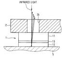
- FIG. 2 is a schematic cross-sectional view for explaining a state where infrared light is irradiated to an SOI substrate shown in FIG. 1 .
- a CMP machine has a wafer support head 2 for supporting several SOI substrates 1 thereon.
- the wafer support head 2 has a disk shape, and the several SOI substrates 1 are attached to an attachment surface 2 a of the disk-shaped wafer support head 2 .
- one of the SOI substrates 1 is attached to the central position of the wafer support head 2 , and the other SOI substrates 1 are attached to surround the SOI substrate 1 on the central position.
- the wafer support head 2 is connected to a drive shaft 3 at the center thereof, and is such constructed that it can be rotated via the drive shaft 3 .
- a torque of the drive shaft 3 is monitored by a torque sensor 4 and can be controlled appropriately.
- the wafer support head 2 is located on a base 6 having a pad 5 for wafer polishing so that the surfaces of the SOI substrates 1 , which are attached to the attachment surface 2 a , are brought in close contact with the pad 5 .
- the wafer support head 2 is so constructed that it can appropriately move on the base 6 in any directions parallel to the pad surface. Therefore, the wafer support head 2 can move above the pad surface while being driven to rotate by the drive shaft 3 .
- a window portion 2 b is formed to pass through the wafer support head 2 at a location where one of the SOI substrate 1 is disposed, and the surface of the wafer can be measured through the window portion 2 b .
- the wafer support head 2 has only to have one window portion 2 b ; however, the wafer support head 2 may have plural window portions 2 b at all of the locations where the SOI substrates 1 are respectively attached to surround the central position of the attachment surface 2 a.
- the CMP machine has a thickness measurement unit 7 for measuring a thickness of an SOI layer.
- the thickness measurement unit 7 is composed of a light source 7 a for irradiating infrared light to the surface of the SOI substrate 1 through the window portion 2 b , a thickness measurement portion 7 b for measuring the thickness of the SOI layer by receiving light reflected by the SOI substrate 1 , and a mirror 7 c for conducting the light reflected by the SOI substrate 1 to the thickness measurement portion 7 b.
- FIG. 2 shows an enlarged view showing a vicinity of the SOI substrate 1 when the surface of the SOI substrate 1 is irradiated with infrared light entering through the window portion 2 b .
- the SOI substrate 1 is composed of a support wafer 11 and an element formation wafer 12 that are bonded together with an oxide film 13 interposed therebetween.
- the surface at the side of the support wafer 11 is attached to the attachment surface 2 a of the wafer support head 2 .
- infrared light incident on the SOI substrate 1 through the window portion 2 b is reflected successively by the surface of the support wafer 11 , the interface between the support wafer 11 and the oxide film 13 , the interface between the oxide film 13 and the element formation wafer 12 , and the surface of the element formation wafer 12 where two parts having different refractive indexes contact each other.
- the reflected lights are conducted to the thickness measurement portion 7 b by the mirror 7 c.
- light that is to be incident on the SOI substrate 1 is required to have a wavelength with which the light can penetrate silicon, and is less liable to be absorbed by silicon and the oxide film. Therefore, although it is not shown, light having the wavelength fulfilling the above conditions is generated by providing a reflection preventive film on an edge face of a semiconductor laser, taking light out to an external resonator, and changing an angle of light by an interference filter disposed on the way of the external resonator.
- infrared light having a wavelength of about 1 to 3 ⁇ m (more preferably, about 1.1 to 1.6 ⁇ m) is used, and the wavelength is varied.
- ⁇ fc ( ⁇ 2 ⁇ q 3 4 ⁇ ⁇ ⁇ 2 ⁇ c 3 ⁇ n * ⁇ ⁇ 0 ) ⁇ ( N m 2 ⁇ ⁇ ) ( 1 )
- ⁇ fc absorption coefficient
- ⁇ wavelength of light
- N impurity concentration
- m effective mass of a free carrier
- ⁇ mobility of the free carrier
- q charge of an electron
- c luminous flux
- n* a real number of refractive index of Si
- ⁇ 0 vacuum dielectric constant
- the thickness measurement portion 7 b Fourier analysis is performed to the intensity-wavelength characteristics of reflected light, and the thickness of the SOI layer that is formed by thinning the element formation wafer 12 is measured.
- the polishing state of the SOI substrate 1 can be measured successively, and the SOI substrate 1 needs not be detached from the polishing machine every time the thickness of the SOI layer is measured.
- the thickness of the SOI layer can be measured easily.
- a semiconductor device including semiconductor elements integrated together and being made dielectric-isolation mutually can be manufactured by performing trench formation and element formation to the side of the element formation wafer 12 of the SOI substrate by well-known methods.
- the window portion may be opened at the base side for measurement, and infrared light may be irradiated through the window portion. In this case, however, the window portion should penetrate the pad.
- the polished surface of the SOI substrate i.e., the surface of the element formation wafer might be damaged to affect element characteristics. Therefore, providing the window portion in the support head 2 as in the aforementioned embodiment is preferable.
- the thickness is measured by irradiating infrared light to the surface opposite to the surface of the SOI substrate 1 that is polished, the infrared light incident thereon is not affected by slurry, the polished surface, and the like. As a result, the measurement accuracy becomes high.
Landscapes
- Engineering & Computer Science (AREA)
- Mechanical Engineering (AREA)
- Physics & Mathematics (AREA)
- Condensed Matter Physics & Semiconductors (AREA)
- General Physics & Mathematics (AREA)
- Manufacturing & Machinery (AREA)
- Computer Hardware Design (AREA)
- Microelectronics & Electronic Packaging (AREA)
- Power Engineering (AREA)
- Mechanical Treatment Of Semiconductor (AREA)
- Finish Polishing, Edge Sharpening, And Grinding By Specific Grinding Devices (AREA)
Abstract
Description

Claims (9)
Applications Claiming Priority (2)
| Application Number | Priority Date | Filing Date | Title |
|---|---|---|---|
| JP32693299A JP2001144059A (en) | 1999-11-17 | 1999-11-17 | Method of manufacturing semiconductor device |
| JP11-326932 | 1999-11-17 |
Publications (1)
| Publication Number | Publication Date |
|---|---|
| US6656755B1 true US6656755B1 (en) | 2003-12-02 |
Family
ID=18193388
Family Applications (1)
| Application Number | Title | Priority Date | Filing Date |
|---|---|---|---|
| US09/709,456 Expired - Fee Related US6656755B1 (en) | 1999-11-17 | 2000-11-13 | Method for manufacturing semiconductor device by polishing |
Country Status (2)
| Country | Link |
|---|---|
| US (1) | US6656755B1 (en) |
| JP (1) | JP2001144059A (en) |
Cited By (4)
| Publication number | Priority date | Publication date | Assignee | Title |
|---|---|---|---|---|
| US20030153136A1 (en) * | 2002-02-14 | 2003-08-14 | Mitsubishi Denki Kabushiki Kaisha | Method of manufacturing semicontor device having trench isolation |
| US20050182594A1 (en) * | 2004-02-04 | 2005-08-18 | Braun David M. | Microdevice processing systems and methods |
| EP3035047A1 (en) * | 2010-11-12 | 2016-06-22 | EV Group E. Thallner GmbH | Measuring device and method for measuring layer thicknesses and defects in a wafer stack |
| US9682458B2 (en) * | 2015-03-18 | 2017-06-20 | Boe Technology Group Co., Ltd. | Method and device for controlling grinding of flexible substrate |
Families Citing this family (6)
| Publication number | Priority date | Publication date | Assignee | Title |
|---|---|---|---|---|
| JP3946470B2 (en) | 2001-03-12 | 2007-07-18 | 株式会社デンソー | Method for measuring thickness of semiconductor layer and method for manufacturing semiconductor substrate |
| JP5339791B2 (en) * | 2008-06-30 | 2013-11-13 | 株式会社東京精密 | Polishing end point detection method and polishing apparatus |
| JP2010188489A (en) * | 2009-02-20 | 2010-09-02 | Covalent Materials Corp | Method for manufacturing bonded wafer |
| JP5387450B2 (en) * | 2010-03-04 | 2014-01-15 | 信越半導体株式会社 | Design method and manufacturing method of SOI wafer |
| GB2478590A (en) * | 2010-03-12 | 2011-09-14 | Precitec Optronik Gmbh | Apparatus and method for monitoring a thickness of a silicon wafer |
| JP5181214B2 (en) * | 2011-02-21 | 2013-04-10 | グローバルウェーハズ・ジャパン株式会社 | Bonded wafer manufacturing method |
Citations (19)
| Publication number | Priority date | Publication date | Assignee | Title |
|---|---|---|---|---|
| US3744916A (en) * | 1971-06-08 | 1973-07-10 | Us Navy | Optical film thickness monitor |
| US5081796A (en) | 1990-08-06 | 1992-01-21 | Micron Technology, Inc. | Method and apparatus for mechanical planarization and endpoint detection of a semiconductor wafer |
| JPH05234971A (en) | 1991-12-27 | 1993-09-10 | Shin Etsu Handotai Co Ltd | Wafer inspecting device |
| JPH05308096A (en) | 1992-04-28 | 1993-11-19 | Shin Etsu Handotai Co Ltd | Method for measuring thickness of monocrystalline thin film in soi substrate |
| JPH05309558A (en) | 1992-05-08 | 1993-11-22 | Komatsu Denshi Kinzoku Kk | Polishing method of laminating wafer |
| JPH074921A (en) | 1993-04-06 | 1995-01-10 | Toshiba Corp | Film-thickness measuring apparatus and polishing apparatus |
| JPH08216016A (en) | 1995-02-14 | 1996-08-27 | Mitsubishi Materials Shilicon Corp | Method of polishing semiconductor wafer and polishing device |
| JPH08316179A (en) | 1995-05-23 | 1996-11-29 | Sony Corp | Flattening method and apparatus in semiconductor process |
| JPH09162087A (en) | 1995-12-06 | 1997-06-20 | Denso Corp | Production of laminated substrate |
| US5838448A (en) * | 1997-03-11 | 1998-11-17 | Nikon Corporation | CMP variable angle in situ sensor |
| JPH1133901A (en) | 1997-07-18 | 1999-02-09 | Nikon Corp | Wafer grinding device |
| US5893796A (en) | 1995-03-28 | 1999-04-13 | Applied Materials, Inc. | Forming a transparent window in a polishing pad for a chemical mechanical polishing apparatus |
| US5964643A (en) | 1995-03-28 | 1999-10-12 | Applied Materials, Inc. | Apparatus and method for in-situ monitoring of chemical mechanical polishing operations |
| JP2000009437A (en) | 1997-10-22 | 2000-01-14 | Hitachi Ltd | Method and apparatus for measuring thickness of thin film, and method and apparatus for manufacturing thin film device using the same |
| JP2000035316A (en) | 1998-07-16 | 2000-02-02 | Nikon Corp | Method and apparatus for measurement of film thickness on wafer |
| US6142855A (en) * | 1997-10-31 | 2000-11-07 | Canon Kabushiki Kaisha | Polishing apparatus and polishing method |
| JP2000353316A (en) | 1999-06-11 | 2000-12-19 | Victor Co Of Japan Ltd | Apparatus for production of magnetic recording medium |
| JP2000354961A (en) | 1999-04-16 | 2000-12-26 | Nikon Corp | Detecting device and detecting method |
| US6190234B1 (en) * | 1999-01-25 | 2001-02-20 | Applied Materials, Inc. | Endpoint detection with light beams of different wavelengths |
-
1999
- 1999-11-17 JP JP32693299A patent/JP2001144059A/en active Pending
-
2000
- 2000-11-13 US US09/709,456 patent/US6656755B1/en not_active Expired - Fee Related
Patent Citations (21)
| Publication number | Priority date | Publication date | Assignee | Title |
|---|---|---|---|---|
| US3744916A (en) * | 1971-06-08 | 1973-07-10 | Us Navy | Optical film thickness monitor |
| US5081796A (en) | 1990-08-06 | 1992-01-21 | Micron Technology, Inc. | Method and apparatus for mechanical planarization and endpoint detection of a semiconductor wafer |
| JPH05234971A (en) | 1991-12-27 | 1993-09-10 | Shin Etsu Handotai Co Ltd | Wafer inspecting device |
| JPH05308096A (en) | 1992-04-28 | 1993-11-19 | Shin Etsu Handotai Co Ltd | Method for measuring thickness of monocrystalline thin film in soi substrate |
| JPH05309558A (en) | 1992-05-08 | 1993-11-22 | Komatsu Denshi Kinzoku Kk | Polishing method of laminating wafer |
| JPH074921A (en) | 1993-04-06 | 1995-01-10 | Toshiba Corp | Film-thickness measuring apparatus and polishing apparatus |
| JPH08216016A (en) | 1995-02-14 | 1996-08-27 | Mitsubishi Materials Shilicon Corp | Method of polishing semiconductor wafer and polishing device |
| US6045439A (en) | 1995-03-28 | 2000-04-04 | Applied Materials, Inc. | Forming a transparent window in a polishing pad for a chemical mechanical polishing apparatus |
| US5893796A (en) | 1995-03-28 | 1999-04-13 | Applied Materials, Inc. | Forming a transparent window in a polishing pad for a chemical mechanical polishing apparatus |
| US5964643A (en) | 1995-03-28 | 1999-10-12 | Applied Materials, Inc. | Apparatus and method for in-situ monitoring of chemical mechanical polishing operations |
| JPH08316179A (en) | 1995-05-23 | 1996-11-29 | Sony Corp | Flattening method and apparatus in semiconductor process |
| JPH09162087A (en) | 1995-12-06 | 1997-06-20 | Denso Corp | Production of laminated substrate |
| US5838448A (en) * | 1997-03-11 | 1998-11-17 | Nikon Corporation | CMP variable angle in situ sensor |
| JPH1133901A (en) | 1997-07-18 | 1999-02-09 | Nikon Corp | Wafer grinding device |
| JP2000009437A (en) | 1997-10-22 | 2000-01-14 | Hitachi Ltd | Method and apparatus for measuring thickness of thin film, and method and apparatus for manufacturing thin film device using the same |
| US6142855A (en) * | 1997-10-31 | 2000-11-07 | Canon Kabushiki Kaisha | Polishing apparatus and polishing method |
| JP2000035316A (en) | 1998-07-16 | 2000-02-02 | Nikon Corp | Method and apparatus for measurement of film thickness on wafer |
| US6261152B1 (en) | 1998-07-16 | 2001-07-17 | Nikon Research Corporation Of America | Heterdoyne Thickness Monitoring System |
| US6190234B1 (en) * | 1999-01-25 | 2001-02-20 | Applied Materials, Inc. | Endpoint detection with light beams of different wavelengths |
| JP2000354961A (en) | 1999-04-16 | 2000-12-26 | Nikon Corp | Detecting device and detecting method |
| JP2000353316A (en) | 1999-06-11 | 2000-12-19 | Victor Co Of Japan Ltd | Apparatus for production of magnetic recording medium |
Non-Patent Citations (3)
| Title |
|---|
| Shio, "Development of Optical in-situ End Detection Mechanism". |
| U.S. Pat. application Ser. No. 09/118,306 (corr. to JP 2000-35316). |
| U.S. Pat. application Ser. No. 09/616,372, Komura, filed Jul. 13, 2000. |
Cited By (11)
| Publication number | Priority date | Publication date | Assignee | Title |
|---|---|---|---|---|
| US20030153136A1 (en) * | 2002-02-14 | 2003-08-14 | Mitsubishi Denki Kabushiki Kaisha | Method of manufacturing semicontor device having trench isolation |
| US6841400B2 (en) * | 2002-02-14 | 2005-01-11 | Renesas Technology Corp. | Method of manufacturing semiconductor device having trench isolation |
| US20050037524A1 (en) * | 2002-02-14 | 2005-02-17 | Renesas Technology Corp. | Method of manufacturing semiconductor device having trench isolation |
| US20060249756A1 (en) * | 2002-02-14 | 2006-11-09 | Renesas Technology Corp. | Method of manufacturing semiconductor device having trench isolation |
| US7144764B2 (en) | 2002-02-14 | 2006-12-05 | Renesas Technology Corp. | Method of manufacturing semiconductor device having trench isolation |
| US20050182594A1 (en) * | 2004-02-04 | 2005-08-18 | Braun David M. | Microdevice processing systems and methods |
| US7299151B2 (en) * | 2004-02-04 | 2007-11-20 | Hewlett-Packard Development Company, L.P. | Microdevice processing systems and methods |
| EP3035047A1 (en) * | 2010-11-12 | 2016-06-22 | EV Group E. Thallner GmbH | Measuring device and method for measuring layer thicknesses and defects in a wafer stack |
| US10008424B2 (en) | 2010-11-12 | 2018-06-26 | Ev Group E. Thallner Gmbh | Measuring device and method for measuring layer thicknesses and defects in a wafer stack |
| US10109538B2 (en) | 2010-11-12 | 2018-10-23 | EV Group E.Thallner GmbH | Measuring device and method for measuring layer thicknesses and defects in a wafer stack |
| US9682458B2 (en) * | 2015-03-18 | 2017-06-20 | Boe Technology Group Co., Ltd. | Method and device for controlling grinding of flexible substrate |
Also Published As
| Publication number | Publication date |
|---|---|
| JP2001144059A (en) | 2001-05-25 |
Similar Documents
| Publication | Publication Date | Title |
|---|---|---|
| US6656755B1 (en) | Method for manufacturing semiconductor device by polishing | |
| JP3270282B2 (en) | Semiconductor manufacturing apparatus and semiconductor device manufacturing method | |
| KR101284520B1 (en) | Method of Polishing a semiconductor-on-insulator structure | |
| KR100458883B1 (en) | Semiconductor wafer with id mark, equipment for and method of manufacturing semiconductor device from them | |
| US5413941A (en) | Optical end point detection methods in semiconductor planarizing polishing processes | |
| JP2821830B2 (en) | Semiconductor thin film device and its application device and method of manufacturing semiconductor thin film device | |
| US5838448A (en) | CMP variable angle in situ sensor | |
| JP2770101B2 (en) | Polishing method of bonded wafer | |
| JP2692659B2 (en) | SOI substrate and method for manufacturing the SOI substrate | |
| US6879029B2 (en) | Semiconductor device having element isolation structure | |
| US5162251A (en) | Method for making thinned charge-coupled devices | |
| US5876819A (en) | Crystal orientation detectable semiconductor substrate, and methods of manufacturing and using the same | |
| US6716722B1 (en) | Method of producing a bonded wafer and the bonded wafer | |
| JPH01312828A (en) | Manufacture of semiconductor | |
| US6313542B1 (en) | Method and apparatus for detecting edges under an opaque layer | |
| JP2870492B2 (en) | SOI substrate and manufacturing method thereof | |
| EP0968081A1 (en) | Flattening process for bonded semiconductor substrates | |
| Nakashima et al. | Characterization of ion implanted and laser annealed polycrystalline Si by a Raman microprobe | |
| US20040188789A1 (en) | Semiconductor device and method for machining a semiconductor substrate | |
| JP4617788B2 (en) | Bonded wafer evaluation method and bonded wafer evaluation apparatus | |
| JPH07142572A (en) | Semiconductor device and manufacture thereof | |
| JP3504796B2 (en) | Method and apparatus for measuring impurities in semiconductors | |
| CN117147441B (en) | A gas detector and a method for preparing the same | |
| US11428645B2 (en) | Wafer inspection device and method of manufacturing semiconductor device by using the wafer inspection device | |
| JPS62122141A (en) | Checking method for semiconductor substrate |
Legal Events
| Date | Code | Title | Description |
|---|---|---|---|
| AS | Assignment |
Owner name: DENSO CORPORATION, JAPAN Free format text: ASSIGNMENT OF ASSIGNORS INTEREST;ASSIGNOR:OHKAWA, MAKOTO;REEL/FRAME:011465/0115 Effective date: 20001023 |
|
| FEPP | Fee payment procedure |
Free format text: PAYOR NUMBER ASSIGNED (ORIGINAL EVENT CODE: ASPN); ENTITY STATUS OF PATENT OWNER: LARGE ENTITY |
|
| FPAY | Fee payment |
Year of fee payment: 4 |
|
| FPAY | Fee payment |
Year of fee payment: 8 |
|
| FEPP | Fee payment procedure |
Free format text: PAYOR NUMBER ASSIGNED (ORIGINAL EVENT CODE: ASPN); ENTITY STATUS OF PATENT OWNER: LARGE ENTITY Free format text: PAYER NUMBER DE-ASSIGNED (ORIGINAL EVENT CODE: RMPN); ENTITY STATUS OF PATENT OWNER: LARGE ENTITY |
|
| REMI | Maintenance fee reminder mailed | ||
| LAPS | Lapse for failure to pay maintenance fees | ||
| STCH | Information on status: patent discontinuation |
Free format text: PATENT EXPIRED DUE TO NONPAYMENT OF MAINTENANCE FEES UNDER 37 CFR 1.362 |
|
| FP | Lapsed due to failure to pay maintenance fee |
Effective date: 20151202 |