US6639293B2 - Solid-state imaging device - Google Patents
Solid-state imaging device Download PDFInfo
- Publication number
- US6639293B2 US6639293B2 US09/996,703 US99670301A US6639293B2 US 6639293 B2 US6639293 B2 US 6639293B2 US 99670301 A US99670301 A US 99670301A US 6639293 B2 US6639293 B2 US 6639293B2
- Authority
- US
- United States
- Prior art keywords
- layer
- type
- semiconductor layer
- impurity concentration
- substrate
- Prior art date
- Legal status (The legal status is an assumption and is not a legal conclusion. Google has not performed a legal analysis and makes no representation as to the accuracy of the status listed.)
- Expired - Lifetime
Links
Images


Classifications
-
- H—ELECTRICITY
- H10—SEMICONDUCTOR DEVICES; ELECTRIC SOLID-STATE DEVICES NOT OTHERWISE PROVIDED FOR
- H10F—INORGANIC SEMICONDUCTOR DEVICES SENSITIVE TO INFRARED RADIATION, LIGHT, ELECTROMAGNETIC RADIATION OF SHORTER WAVELENGTH OR CORPUSCULAR RADIATION
- H10F39/00—Integrated devices, or assemblies of multiple devices, comprising at least one element covered by group H10F30/00, e.g. radiation detectors comprising photodiode arrays
- H10F39/10—Integrated devices
- H10F39/12—Image sensors
- H10F39/18—Complementary metal-oxide-semiconductor [CMOS] image sensors; Photodiode array image sensors
-
- H—ELECTRICITY
- H10—SEMICONDUCTOR DEVICES; ELECTRIC SOLID-STATE DEVICES NOT OTHERWISE PROVIDED FOR
- H10F—INORGANIC SEMICONDUCTOR DEVICES SENSITIVE TO INFRARED RADIATION, LIGHT, ELECTROMAGNETIC RADIATION OF SHORTER WAVELENGTH OR CORPUSCULAR RADIATION
- H10F77/00—Constructional details of devices covered by this subclass
- H10F77/10—Semiconductor bodies
- H10F77/14—Shape of semiconductor bodies; Shapes, relative sizes or dispositions of semiconductor regions within semiconductor bodies
Definitions
- the present invention relates to a solid-state imaging device and to a semiconductor photoelectric conversion device having a photoelectric conversion element such as a photodetector of a photocoupler, and more particularly to a solid-state imaging device that is interchangeable in fabricating processes with a CMOS (Complementary Metal-Oxide Semiconductor) device, i.e., a CMOS image sensor.
- CMOS Complementary Metal-Oxide Semiconductor
- CCD Charge coupled device
- a CCD image sensor is a type of image sensor in which photoelectric conversion elements or photodiodes are arranged two-dimensionally corresponding to pixels (picture elements), the signals of respective pixels that have become electric charges by means of photoelectric conversion elements being read sequentially using vertical transmission CCDs and horizontal transmission CCDs.
- CMOS image sensors are similar to CCD image sensors in that photoelectric conversion elements are arranged two-dimensionally corresponding to pixels, but in reading signals, rather than using vertical and horizontal transmission CCDs, signals stored for respective pixels are read from selected picture elements by means of selection lines constituted by aluminum lines, as in the read-out of a semiconductor memory device.
- CMOS image sensor In contrast with a CCD image sensor, which requires a plurality of positive and negative power source voltages for driving the CCDs, a CMOS image sensor can be driven by a single power supply and enables lower power consumption and lower power source voltage than a CCD image sensor. Furthermore, the use of a fabrication process for the CCD itself in the fabrication of a CCD image sensor complicates the straightforward application of fabrication processes that are typically used for a CMOS circuit. In contrast, the fabrication processes used for a CMOS image sensor are also commonly used for CMOS circuits.
- CMOS image sensor Peripheral circuits such as logic circuits, analog circuits and analog/digital conversion circuits can therefore be formed simultaneously with the CMOS image sensor by means of CMOS fabrication processes that are often used in the fabrication of processors, semiconductor memory devices such as DRAMs (Dynamic Random Access Memories), and logic circuits.
- CMOS image sensor has the advantages that it can easily be formed on the same semiconductor chip as semiconductor memory device or a processor, and in addition, the fabrication of the CMOS image sensor can easily share the same manufacturing plant as a semiconductor memory device or processor.
- FIG. 1 is a schematic plan view showing an example of this type of CMOS image sensor and shows the floor plan of a semiconductor device that is formed as a CMOS image sensor.
- CMOS image sensor 1 is provided with: imaging unit 2 in which photoelectric conversion elements are arranged two-dimensionally for each pixel; timing generator 3 for generating timing signals that are necessary for reading signals from the pixels; vertical scanning unit 4 and horizontal scanning unit 5 for selecting the output of pixels; analog signal processor 6 for amplifying and processing signals from selected pixels; and logic circuit unit 7 for processing the analog signal output from analog signal processor 6 and outputting the result as digital signals.
- Logic circuit unit 7 is provided with: A/D converter 8 for performing analog-to-digital conversion of the input analog signals; digital signal processor (DSP) 9 for converting the digitized signals to digital image signals; and interface (I/F) 10 for outputting digital image signals to the outside and receiving command data from the outside.
- A/D converter 8 for performing analog-to-digital conversion of the input analog signals
- DSP digital signal processor
- I/F interface
- FIG. 2 is a schematic sectional view showing the construction of an unit cell of the prior art in a CMOS image sensor.
- Unit cell 11 has fundamentally a construction in which a p-type well region 13 is provided on p ⁇ -type substrate 12 , and n-type photoelectric conversion region 14 which joins p-type well region 13 to form a photodiode is provided in the surface of p-type well region 13 .
- p + -type isolation region 15 that is formed in p-type well region 13 ; isolation oxide film 16 formed on, for example, p + -type isolation region 15 ; gate oxide film 17 which is formed on portions of the surfaces of p-type well region 13 and n-type photoelectric conversion region 14 other than the region in which isolation oxide film 16 is formed; interlayer insulation film 18 which is formed so as to cover the entire surfaces of isolation oxide film 16 and gate oxide film 17 ; and shield film 19 which is formed in interlayer insulation film 18 for preventing the incidence of light to unnecessary portions.
- n + -type reset drain region 20 is formed in p-type well region 13 at a position that is somewhat separated from n-type photoelectric conversion region 14 .
- Gate oxide film 17 is also formed on the surface of this n + -type reset drain region 20 .
- Reset transistor 21 is formed which takes the region that is within p-type well region 13 and between n-type photoelectric conversion region 14 and n + -type reset drain region 20 as the channel region, n-type photoelectric conversion region 14 as the source region, and n + -type reset drain region 20 as the drain region.
- N-type photoelectric conversion region 14 is thus connected to n + -type reset drain region 20 by way of reset transistor 21 .
- Unit cell 11 is further provided with driver transistor 22 of a source follower, and transistor 23 , which is a horizontal selection switch.
- N-type photoelectric conversion region 14 is connected to the gate of driver transistor 22 for outputting to the outside output changes according to the amount of incident light.
- Load transistor 24 of a source follower is formed for each row of the unit cell array.
- Driver transistor 22 , transistor 23 , and load transistor 24 are inserted in that order in a series between power supply voltages V DD and V SS .
- the voltage output V out of this unit cell 11 is obtained from the connection point between transistor 23 and load transistor 24 .
- a CMOS image sensor of this construction operates as follows.
- raising a pulse which is applied to the gate of reset transistor 21 to a high level sets the potential of n-type photoelectric conversion region 14 to the power supply voltage V DD which is applied to n + -type reset drain region 20 and thus resets the signal charge in n-type photoelectric conversion region 14 .
- Lowering the pulse which is applied to the gate of reset transistor 21 to a low level brings about the start of accumulation of signal charge.
- the incidence of light generates electron-hole pairs in the region of the lower portion of n-type photoelectric conversion region 14 , whereupon the electrons are accumulated in the depletion layer below n-type photoelectric conversion region 14 and the holes are discharged through p-type well region 13 .
- n-type photoelectric conversion region 14 changes according to the number of accumulated electrons, and by the operation of the source follower, this change in potential is outputted by way of the source of driver transistor 22 to horizontal selection switch transistor 23 , whereby a photoelectric conversion output characteristic having good linearity can be obtained.
- kTC Error Correction Noise occurs in n-type photoelectric conversion region 14 , which becomes a floating diffusion layer, when reset transistor 21 is reset, this noise can be eliminated by sampling and storing output during darkness before transmitting signal electrons and then finding the difference between this and bright output.
- k is Boltzmann's constant
- T temperature
- C electrical capacitance
- FIG. 3 is a schematic sectional view showing the a photodiode structure which provides greater reduction of leak noise than the photoelectric conversion element (photodiode) in the unit cell shown in FIG. 2 .
- parts bearing the same reference numerals as parts in FIG. 2 are the same constituent elements as in FIG. 2 .
- the photodiode structure shown in FIG. 3 includes surface p + -layer 25 formed on the surface of the photodiode (i.e., photoelectric conversion element) portion in FIG. 2, and the provision of this type of surface p + -layer 25 reduces leak current on the surface of the photodiode portion.
- This type of construction is well used in the prior art.
- a solution to these problems calls for an improvement in the photoelectric conversion efficiency per unit area. Since the pixels are smaller, the amount of light that is incident to each pixel also decreases. Regardless of this decrease in the amount of incident light, the photoelectric conversion efficiency in the direction of depth of the photodiode must be improved in order to increase photoelectrons, i.e., a deep photodiode must be formed. Forming a deep photodiode means extending the depletion layer of the photodiode deep into the substrate.
- the assignees of the present invention have previously proposed in JP, P2001-7309A a method in which the impurity concentration of only the p-type well layer below the photodiode is made lower than the impurity concentration of the p-type well of other portions, thereby extending the depletion layer of the photodiode more deeply into the substrate and improving sensitivity to light, and moreover, reducing capacitive coupling with the substrate to improve detection sensitivity.
- This problem involves the occurrence of crosstalk between pixels and the substantial decrease in resolution due to the movement of electrons between neighboring photodiodes (i.e., unit cells).
- the diffusion of photoelectrons in pixels in which light is generated results in the leakage of electrons into pixels in which there should be no incident light to begin with, and noise is thus generated that gives the appearance of signal input even in these pixels in which there is no incident light.
- Contrivances such as shield films are unable to suppress this crosstalk component because it originates from the generation of photoelectrons in relatively deep portions of the substrate.
- Light that results in photoelectrons in relatively deep portions of the substrate is light of wavelengths ranging from red to near-infrared.
- blue and green light which is visible light of short wavelengths, is substantially absorbed within portions of the n-type photoelectric conversion region and depletion layer of the photodiode that spread in the direction of the substrate, and this light therefore does not penetrate deep into the substrate.
- the crosstalk component which passes through the substrate is small for short wavelengths.
- IR cutoff filters are often used to suppress sensitivity to near-infrared light, but if sensitivity to near-infrared light is too great, sensitivity to light that passes through the filter cannot be ignored regardless of the use of the IR cutoff filter.
- the object of the present invention is realized by a solid-state imaging device which includes: a substrate layer which is composed of a semiconductor of a first conductive type; a semiconductor layer of the first conductive type which is provided on the substrate layer; and a photoelectric conversion region of a second conductive type, which is the opposite conductive type of the first conductive type, provided on the semiconductor layer; wherein the impurity concentration of the substrate layer is higher than the impurity concentration of the semiconductor layer.
- a low-impurity concentration semiconductor layer of the first conductive type having a lower impurity concentration than the semiconductor layer may be provided between the substrate layer and the semiconductor layer.
- the impurity concentration of the low-impurity concentration semiconductor layer is preferably lower than the impurity concentration of the photoelectric conversion region.
- the solid-state imaging device of the present invention may further be provided with a peripheral circuit semiconductor layer of the first conductive type that has a higher impurity concentration than the semiconductor layer and that is formed on the semiconductor layer at least below transistors in pixels.
- the distance from the surface of the main plane of the semiconductor to the surface of the semiconductor layer on the substrate layer side is preferably a minimum of 2 ⁇ m and a maximum of 10 ⁇ m.
- At least one of the semiconductor layer and the low-impurity density semiconductor layer is preferably formed by epitaxial growth. Further, the depth profile of the impurity in the semiconductor layer is preferably a retrograde profile.
- the present invention can realize a photodiode that is capable of high sensitivity, can cause the spectral characteristic to approach the spectral characteristic of visible light, and further, can provide a solid-state imaging device that suppresses crosstalk between pixels.
- FIG. 1 is a schematic plan view showing the construction of one example of a CMOS image sensor
- FIG. 2 is a schematic sectional view showing an unit cell and a peripheral circuit in a CMOS image sensor of the prior art
- FIG. 3 is a schematic sectional view showing an unit cell of the prior art in which leak noise in a photodiode has been reduced;
- FIG. 4 is a schematic sectional view showing an unit cell in a solid-state imaging device according to a first embodiment of the present invention
- FIG. 5 is a schematic sectional view showing an unit cell in a solid-state imaging device according to a second embodiment of the present invention.
- FIG. 6 shows the depth profile of the impurity in a photodiode portion in the solid state imaging device shown in FIG. 5;
- FIG. 7 is a graph showing the spectral sensitivity characteristic in a solid-state imaging device of the prior art and the solid-state imaging device shown in FIG. 5;
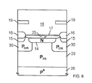
- FIG. 8 is a schematic sectional view showing an unit cell in a solid-state imaging device according-to a third embodiment of the present invention.
- FIG. 9 is a schematic sectional view showing an unit cell in a solid-state imaging device according to a fourth embodiment of the present invention.
- a solid-state imaging device whose unit cell is shown in FIG. 4 is formed as the CMOS image sensor of type shown in the above-described FIG. 1 .
- the construction and operation of portions other than the unit cell are equivalent to the CMOS image sensor shown in FIG. 1 and redundant explanation is therefore omitted.
- parts in FIG. 4 that have the same reference numerals as parts in FIG. 2 are identical to the constituent elements in FIG. 2 .
- p-type layer 27 having an impurity concentration that is lower than substrate p + -layer 26 is formed on substrate p + -layer 26 , which is a high-concentration p-type semiconductor substrate (for example, a silicon p + -type substrate).
- N-type photoelectric conversion region 14 is formed at a location on the upper side of this p-type layer 27 .
- Substrate p + -layer 26 , p-type layer 27 , and n-type photoelectric conversion region 14 correspond to the substrate layer of the first conductive type, the semiconductor layer of the first conductive type, and the photoelectric conversion region of the second conductive type, respectively.
- N-type photoelectric conversion region 14 is formed by, for example, ion implantation or diffusion of an n-type impurity in p-type layer 27 .
- P-type layer 27 is preferably formed on substrate p + -layer 26 by epitaxial growth.
- the impurity profile may be controlled by ion implantation of a p-type impurity as in the second embodiment to be explained hereinbelow.
- the impurity concentration of substrate p + -layer 26 is, for example, 1 ⁇ 10 18 /cm 3 to 1 ⁇ 10 22 /cm 3
- the impurity concentration of p-type layer 26 is, for example, 1 ⁇ 10 16 /cm 3 to 1 ⁇ 10 18 /cm 3
- the impurity concentration of n-type photoelectric conversion region 14 is, for example, 1 ⁇ 10 18 /cm 3 to 1 ⁇ 10 22 /cm 3 .
- P + -type isolation regions 15 and isolation oxide films 16 are provided for device isolation at both ends of the upper surface of p-type layer 27 that is shown in the figure, and in addition, as with the unit cell of the prior art that is shown in FIG. 3, surface p + -layer 25 is formed on the surfaces of p-type layer 27 and n-type photoelectric conversion region 14 other than the formation region of isolation oxide layers 16 to prevent leaks at the surface of the photodiode portion.
- Interlayer insulation film 18 is provided on isolation oxide films 16 and surface p + -layer 25 so as to cover the entire solid-state imaging device that includes this unit cell. Shield films 19 are formed in interlayer insulation film 18 to prevent the incidence of light to portions that do not require light.
- the thickness of p-type layer 27 in this unit cell is set to from approximately 2 ⁇ m to 10 ⁇ m.
- the distance from the surface of the semiconductor main plane to the interface between p-type layer 27 and substrate p + -layer 26 is set to a minimum of 2 ⁇ m and a maximum 10 ⁇ m. This range from 2 ⁇ m to 10 ⁇ m is substantially equal to the absorption length of light of the red or near-infrared region in silicon.
- the thickness of p-type layer 27 can be changed according to the wavelength of light for which sensitivity is required.
- n-type photoelectric conversion region 14 and p-type layer 27 When incident light enters a photodiode that is made up by n-type photoelectric conversion region 14 and p-type layer 27 , the incidence of light generates electron-hole pairs in n-type photoelectric conversion region 14 and the region of p-type layer 27 that is below n-type photoelectric conversion region 14 during a signal charge accumulation period. The generated electrons are then accumulated in the depletion layer that is formed in n-type photoelectric conversion region 14 and the portion of p-type layer 27 that lies below n-type photoelectric conversion region 14 .
- substrate p + -layer 26 which has a higher impurity concentration than p-type layer 27 , is arranged below p-type layer 27 , electrons of the photoelectrons occurring in p-type layer 27 at this time that diffuse in the direction of the substrate are reliably captured in substrate p + -layer 26 , recombined, and annihilated. Electron diffusion in the horizontal direction is therefore more greatly suppressed in the unit cell shown in FIG. 4 than in the unit cell of the prior art. As a result, crosstalk between pixels can be reduced, thereby enabling a suppression of a drop in image resolution.
- the solid-state imaging device according to the second embodiment shown in FIG. 5 is formed as a CMOS image sensor such as the previously described device shown in FIG. 1 . Redundant explanation regarding the construction and operation of parts other than the unit cell is accordingly omitted here.
- parts in FIG. 5 that are identified by the same reference numerals as used in FIG. 4 are the same constituent elements as the parts in FIG. 4 .
- P-layer 28 has an impurity concentration that is lower than that of p-type layer 27 , and thus, has an impurity concentration that is considerably lower than that of substrate p + -layer 26 .
- P ⁇ -layer 28 corresponds to the low-impurity concentration semiconductor layer of the first conductive type, and is provided on substrate p + -layer 26 , preferably by means of epitaxial growth.
- the impurity concentration of p ⁇ -layer 28 is preferably set lower than the impurity concentration in n-type photoelectric conversion region 14 .
- the impurity concentration of substrate p + -layer 26 is, for example, from 1 ⁇ 10 18 /cm 3 to 1 ⁇ 10 22 /cm 3 ; the impurity concentration of p ⁇ -layer 28 is, for example, from 1 ⁇ 10 14 /cm 3 to 1 ⁇ 10 16 /cm 3 , and the impurity concentration of p-type layer 27 is, for example, from 1 ⁇ 10 16 /cm 3 to 1 ⁇ 10 18 /cm 3 .
- the impurity concentration of n-type photoelectric conversion region 14 is, for example, 1 ⁇ 10 18 /cm 3 to 1 ⁇ 10 22 /cm 3 .
- p ⁇ -layer 28 and p-type layer 27 can be grown on substrate p + -layer 26 in the same epitaxial step, following which a p-type impurity can be introduced in only the appropriate portions of p-type layer 27 by ion implantation.
- the thickness of p-type layer 27 is determined by the maximum range of impurities at the time of ion implantation. Because the thickness of p-type layer 27 in this unit cell is also preferably set to between 2 ⁇ m and 10 ⁇ m, the ion energy during implantation is adjusted according to the desired thickness.
- the location of maximum impurity concentration is not at the surface of p-type layer 27 but in the interior, and ion implantation is preferably carried out at a relatively high energy such that the distribution of impurity concentration in the direction of depth, that is, a depth profile, is a retrograde profile.
- FIG. 6 shows an impurity concentration profile in the direction of depth of a photodiode of the unit cell shown in FIG. 5 .
- the impurity concentration of substrate p + -layer 26 is high
- the concentration in n-type photoelectric conversion region 14 and p-type layer 27 is medium
- the concentration in p ⁇ -layer 28 is low.
- the extent of the photoelectric conversion region which acts as depletion layer is the portion indicated by an arrow, its direction in depth extending from n-type photoelectric conversion region 14 to the middle portion in the direction of depth of p-type layer 27 .
- Photoelectrons that are generated in deeper portions than the middle of p-type layer 27 are effectively diffused in the direction of player 28 , and even electrons that do diffuse in the horizontal direction do not again reach the depletion layer on the surface side and do not contribute to sensitivity. In other words, the diffusion of electrons is substantially suppressed. Electrons that reach p-layer 28 are recombined and annihilated in substrate p + -layer 26 and therefore also make no contribution to sensitivity. The diffusion of electrons in the horizontal direction is thus suppressed, and crosstalk between pixels can be reduced.
- the unit cell of the second embodiment further has the advantage of allowing easy control of the spectral characteristic of the photodiode.
- FIG. 7 is a graph showing the spectral sensitivity of the unit cell of the second embodiment and an unit cell of the prior art.
- the determinant of spectral sensitivity, and in particular, sensitivity to the near-infrared portion is the extension of the depletion layer in the direction of depth, and more specifically, the depth (and profile) of p-type layer 27 .
- Contributions to the sensitivity at portions that are deeper than p-type layer 27 can be reduced by appropriately controlling this position of p-type layer 27 , and particularly, the position of the maximum impurity concentration.
- controlling only the extension in the direction of depth of p-type layer 27 effectively suppresses only sensitivity to near-infrared light and, compared to the example of the prior art, does not reduce sensitivity to shorter wavelengths of visible light (from 350 nm to 550 nm).
- the solid-state imaging device according to the third embodiment shown in FIG. 8 is formed as the previously described CMOS image sensor shown in FIG. 1, and redundant explanation of the construction and operation of parts other than the unit cell is therefore omitted.
- parts in FIG. 8 bearing the same reference numerals as parts in FIG. 4 are constituent elements equivalent to those in FIG. 4 .
- the unit cell shown in FIG. 8 is substantially the same as the cell shown in FIG. 4 but differs in that p-type layer 27 in the unit cell shown in FIG. 4 is made up by photodiode p-type layer 29 indicated by P PD and peripheral circuit p-type layer 30 indicated by P CIR .
- Photodiode p-type layer 29 is provided at least in the region that is directly below n-type photoelectric conversion region 14 so as to contact both n-type photoelectric conversion region 14 and substrate p + -layer 26 .
- Peripheral circuit p-type layer 30 is provided as a well region that is formed in photodiode p-type layer 29 and is provided to constitute transistors in pixels such as transistors of horizontal selection switches and driver transistors. Photodiode p-type layer 29 and peripheral circuit p-type layer 30 correspond to the semiconductor layer of the first conductive type and the peripheral circuit layer of the first conductive type, respectively.
- Peripheral circuit p-type layer 30 itself does not directly join substrate p + -layer 26 .
- N-type photoelectric conversion region 14 is formed by ion implantation or n-type impurity diffusion in photodiode p-type layer 29 .
- the impurity concentration of substrate p + -layer 26 is, for example, 1 ⁇ 10 18 /cm 3 to 1 ⁇ 10 22 /cm 3
- the impurity concentration of photodiode p-type layer 29 and peripheral circuit p-type layer 30 is, for example, 1 ⁇ 10 16 /cm 3 to 1 ⁇ 10 18 /cm 3
- the impurity concentration of photodiode p-type layer 29 is lower than the impurity concentration of peripheral circuit p-type layer 30 .
- the impurity concentration of n-type photoelectric conversion region 14 is, for example, 1 ⁇ 10 18 /cm 3 to 1 ⁇ 10 22 /cm 3 .
- Photodiode p-type layer 29 and peripheral circuit p-type layer 30 are, for example, grown on substrate p + -layer 26 by epitaxial growth and formed by the desired ion implantation.
- the arrangement of substrate p + -layer 26 having a higher impurity concentration than photodiode p-type layer 29 below photodiode p-type layer 29 means that, of the photoelectrons that have been generated in photodiode p-type layer 29 , electrons that are diffused in the direction of the substrate are reliably captured in substrate p + -layer 26 and then recombined and annihilated.
- the unit cell shown in FIG. 8 therefore provides greater suppression of horizontal electron diffusion than the unit cell of the prior art. Crosstalk between pixels can therefore be reduced, and decrease in image resolution can be suppressed.
- this unit cell is capable of providing greater suppression of the diffusion of electrons and reducing crosstalk than the unit cell shown in FIG. 4 because peripheral circuit p-type layer 30 is formed below transistors in the pixels, and the p-type impurity concentration of this layer is higher than that of photodiode p-type layer 29 .
- the solid-state imaging device according to the fourth embodiment shown in FIG. 9 is formed as the previously described CMOS image sensor shown in FIG. 1, and redundant explanation regarding the construction and operation of parts other than the unit cell is here omitted.
- parts in FIG. 9 bearing the same reference numerals as parts in FIG. 8 are the same constituent elements as the parts in FIG. 8 .
- p-layer 28 having a lower impurity concentration than photodiode p-type layer 29 between substrate p + -layer 26 and photodiode p-type layer 29 , as in the second embodiment.
- P ⁇ -layer 28 is provided on substrate p + -layer 26 , preferably by epitaxial growth.
- p-layer 28 , photodiode p-type layer 29 , and peripheral circuit p-type layer 30 can be formed in the same epitaxial step and p-type impurities can be introduced into only appropriate parts of photodiode p-type layer 29 and peripheral circuit p-type layer 30 by ion implantation, as in the second embodiment.
- the preferable impurity profile for photodiode p-type layer 29 is the same as the impurity profile of p-type layer 27 in the second embodiment.
- the impurity concentration of substrate p + -layer 26 is, for example, 1 ⁇ 10 18 /cm 3 to 1 ⁇ 10 22 /cm 3 ;
- the impurity concentration of p ⁇ -layer 28 is, for example, 1 ⁇ 10 14 /cm 3 to 1 ⁇ 10 16 /cm 3 ;
- the impurity concentration of photodiode p-type layer 29 and peripheral circuit p-type layer 30 is, for example, 1 ⁇ 10 16 /cm 3 to 1 ⁇ 10 18 /cm 3 .
- the impurity concentration of photodiode p-type layer 29 is lower than that of peripheral circuit p-type layer 30 .
- the impurity concentration of n-type photoelectric conversion region 14 is, for example, 1 ⁇ 10 18 /cm 3 to 1 ⁇ 10 22 /cm 3 .
- the incident light when incident light enters a photodiode that is made up by n-type photoelectric conversion region 14 and photodiode p-type layer 29 , the incident light generates electron-hole pairs in n-type photoelectric conversion region 14 and the region of photodiode p-type layer 29 that underlies n-type photoelectric conversion region 14 during the signal charge accumulation period.
- the generated electrons are accumulated in the depletion layer that is formed in n-type photoelectric conversion region 14 and the region of photodiode p-type layer 29 that underlies n-type photoelectric conversion region 14 .
- this unit cell is thus capable of providing greater suppression of the horizontal diffusion of electrons than the prior-art unit cell.
- this unit cell is capable of reducing crosstalk between pixels and suppressing decrease in image resolution.
- peripheral circuit p-type layer 30 is formed below transistors in pixels and because the p-type impurity concentration of this layer is higher than that of photodiode p-type layer 29 , this unit cell can provide greater suppression of electron diffusion and keep crosstalk to a lower level than an unit cell of the second embodiment.
- the junction position of substrate p + -layer 26 with p-type layer 27 or photodiode p-type layer 30 in these embodiments is preferably not too shallow or sensitivity will be reduced and transistor characteristics altered.
- the junction position is preferably approximately from 2 ⁇ m to 10 ⁇ m, which is deeper than the p-type well of the prior art.
- the thickness of p-type layer 27 or photodiode p-type layer 30 is preferably from 2 ⁇ m to 10 ⁇ m, which includes the thickness of n-type photoelectric conversion region 14 and surface p + -layer 25 .
- Substrate p + -layer 26 itself can be formed on some type of silicon semiconductor substrate by epitaxial growth.
- the use of such a substrate p + -layer that has been produced by epitaxial growth has the advantages of reducing flaws and eliminating noise.
- the substrate may have any impurity concentration at portions that are deeper than this substrate p + -layer, and the above-described object can be realized by using this p-on-p + -substrate.
- the invention is not limited to this photodiode structure and obviously may be applied to a photodiode that lacks surface p + -layer 25 on the photodiode surface.
- the present invention is not limited to the above-described CMOS image sensor and can obviously be applied to a one-dimensional CMOS sensor (i.e., “line sensor”) or photocoupler having a photodiode structure.
- the present invention includes within its scope a construction in which the conductive type of each layer is reversed in the above-described embodiments, for example, a construction that uses a substrate n + -layer, an n-type layer, and a p-type photoelectric conversion region in place of a substrate p + -layer, a p-type layer, and a n-type photoelectric conversion region and in which holes are accumulated in a depletion layer.
- a high-concentration substrate layer of the first conductive type which is a substrate p + -layer, is formed below a semiconductor layer of a first conductive type such as a p-type layer or a photodiode p-type layer.
- a semiconductor layer of a first conductive type such as a p-type layer or a photodiode p-type layer.
- the device of the present invention therefore provides greater suppression of horizontal electron diffusion than a device of the prior art and thus enables a further reduction of crosstalk between pixels, and consequently, can suppress loss in image resolution.
- controlling the distribution of impurity in the direction of depth in the semiconductor layer enables effective suppression of only near-infrared light without reducing sensitivity to shorter wavelengths (from 350 nm to 550 nm) of visible light.
- a solid-state imaging device can be obtained that is amenable to use as a device for visible light.
Landscapes
- Solid State Image Pick-Up Elements (AREA)
- Light Receiving Elements (AREA)
Abstract
Description
Claims (11)
Applications Claiming Priority (2)
| Application Number | Priority Date | Filing Date | Title |
|---|---|---|---|
| JP2000-365525 | 2000-11-30 | ||
| JP2000365525A JP4270742B2 (en) | 2000-11-30 | 2000-11-30 | Solid-state imaging device |
Publications (2)
| Publication Number | Publication Date |
|---|---|
| US20020063302A1 US20020063302A1 (en) | 2002-05-30 |
| US6639293B2 true US6639293B2 (en) | 2003-10-28 |
Family
ID=18836282
Family Applications (1)
| Application Number | Title | Priority Date | Filing Date |
|---|---|---|---|
| US09/996,703 Expired - Lifetime US6639293B2 (en) | 2000-11-30 | 2001-11-30 | Solid-state imaging device |
Country Status (5)
| Country | Link |
|---|---|
| US (1) | US6639293B2 (en) |
| JP (1) | JP4270742B2 (en) |
| KR (1) | KR20020042508A (en) |
| DE (1) | DE10160501A1 (en) |
| TW (1) | TW517388B (en) |
Cited By (19)
| Publication number | Priority date | Publication date | Assignee | Title |
|---|---|---|---|---|
| US6756618B2 (en) * | 2002-11-04 | 2004-06-29 | Hynix Semiconductor Inc. | CMOS color image sensor and method for fabricating the same |
| US20040262609A1 (en) * | 2003-06-25 | 2004-12-30 | Chandra Mouli | Reduced barrier photodiode/transfer gate device structure of high efficiency charge transfer and reduced lag and method of formation, and |
| US20050184321A1 (en) * | 2004-02-25 | 2005-08-25 | National Semiconductor Corporation | Low dark current CMOS image sensor pixel having a photodiode isolated from field oxide |
| US20050263676A1 (en) * | 2003-10-01 | 2005-12-01 | Dongbu Electgronics Co., Ltd. | Complementary metal oxide semiconductor image sensor and method for fabricating the same |
| US20060261385A1 (en) * | 2005-05-23 | 2006-11-23 | Micron Technology, Inc. | Phase shift transparent structures for imaging devices |
| US20070029926A1 (en) * | 2005-08-04 | 2007-02-08 | Taiwan Oasis Technology Co., Ltd. | Multi-wavelength LED construction & manufacturing process |
| US7307327B2 (en) | 2005-08-04 | 2007-12-11 | Micron Technology, Inc. | Reduced crosstalk CMOS image sensors |
| US20080006893A1 (en) * | 2006-07-10 | 2008-01-10 | Nec Electronics Corporation | Solid-state image pickup device |
| US20090038540A1 (en) * | 2005-09-12 | 2009-02-12 | Shin-Etsu Handotai Co., Ltd. | Method for Manufacturing Epitaxial Wafer and Epitaxial Wafer Manufactured by this Method |
| US20110062542A1 (en) * | 2009-09-17 | 2011-03-17 | International Business Machines Corporation | Structures, design structures and methods of fabricating global shutter pixel sensor cells |
| US20110163407A1 (en) * | 2003-12-12 | 2011-07-07 | Canon Kabushiki Kaisha | Photoelectric conversion device, method of manufacturing photoelectric conversion device, and image pickup system |
| US8790949B2 (en) * | 2011-03-23 | 2014-07-29 | Sony Corporation | Solid state imaging device, method of producing solid state imaging device, and electronic apparatus |
| US9761618B2 (en) | 2013-10-07 | 2017-09-12 | Canon Kabushiki Kaisha | Solid-state imaging apparatus, method for manufacturing the same, and imaging system |
| US10304881B1 (en) * | 2017-12-15 | 2019-05-28 | Atomera Incorporated | CMOS image sensor with buried superlattice layer to reduce crosstalk |
| US10355151B2 (en) | 2017-12-15 | 2019-07-16 | Atomera Incorporated | CMOS image sensor including photodiodes with overlying superlattices to reduce crosstalk |
| US10361243B2 (en) | 2017-12-15 | 2019-07-23 | Atomera Incorporated | Method for making CMOS image sensor including superlattice to enhance infrared light absorption |
| US10396223B2 (en) * | 2017-12-15 | 2019-08-27 | Atomera Incorporated | Method for making CMOS image sensor with buried superlattice layer to reduce crosstalk |
| US10461118B2 (en) | 2017-12-15 | 2019-10-29 | Atomera Incorporated | Method for making CMOS image sensor including photodiodes with overlying superlattices to reduce crosstalk |
| US10741602B2 (en) * | 2015-05-06 | 2020-08-11 | Cista System Corp. | Back side illuminated CMOS image sensor arrays |
Families Citing this family (41)
| Publication number | Priority date | Publication date | Assignee | Title |
|---|---|---|---|---|
| KR20030057707A (en) * | 2001-12-29 | 2003-07-07 | 주식회사 하이닉스반도체 | Method for fabricating image sensor |
| US6838186B2 (en) | 2002-04-22 | 2005-01-04 | Polinas Plastic Of America, Inc. | Multilayer oriented antimicrobial and antifogging films |
| KR100873288B1 (en) * | 2002-07-05 | 2008-12-11 | 매그나칩 반도체 유한회사 | Image sensor and manufacturing method |
| US6949445B2 (en) * | 2003-03-12 | 2005-09-27 | Micron Technology, Inc. | Method of forming angled implant for trench isolation |
| KR100549589B1 (en) * | 2003-09-29 | 2006-02-08 | 매그나칩 반도체 유한회사 | Image sensor and its manufacturing method |
| JP4612818B2 (en) * | 2004-08-31 | 2011-01-12 | キヤノン株式会社 | Solid-state imaging device, solid-state imaging device, and imaging system |
| CN101369594B (en) * | 2003-12-12 | 2012-06-27 | 佳能株式会社 | Photoelectric conversion device, method of manufacturing the same, and imaging system |
| JP2005209695A (en) | 2004-01-20 | 2005-08-04 | Toshiba Corp | Solid-state imaging device and manufacturing method thereof |
| WO2005109512A1 (en) * | 2004-05-06 | 2005-11-17 | Canon Kabushiki Kaisha | Photoelectric conversion device and manufacturing method thereof |
| JP5230058B2 (en) * | 2004-06-07 | 2013-07-10 | キヤノン株式会社 | Solid-state imaging device and camera |
| US7605415B2 (en) * | 2004-06-07 | 2009-10-20 | Canon Kabushiki Kaisha | Image pickup device comprising photoelectric conversation unit, floating diffusion region and guard ring |
| JP4530747B2 (en) | 2004-07-16 | 2010-08-25 | 富士通セミコンダクター株式会社 | Solid-state imaging device and manufacturing method thereof |
| US7880255B2 (en) * | 2004-07-19 | 2011-02-01 | Micron Technology, Inc. | Pixel cell having a grated interface |
| US7385238B2 (en) * | 2004-08-16 | 2008-06-10 | Micron Technology, Inc. | Low dark current image sensors with epitaxial SiC and/or carbonated channels for array transistors |
| JP4646577B2 (en) * | 2004-09-01 | 2011-03-09 | キヤノン株式会社 | Photoelectric conversion device, manufacturing method thereof, and imaging system |
| JP2006108485A (en) * | 2004-10-07 | 2006-04-20 | Sanyo Electric Co Ltd | Solid-state imaging device |
| JP4770276B2 (en) * | 2005-06-01 | 2011-09-14 | 船井電機株式会社 | Solid-state imaging device and solid-state imaging device |
| JP4679340B2 (en) * | 2005-11-11 | 2011-04-27 | 株式会社東芝 | Solid-state imaging device |
| JP4857773B2 (en) * | 2006-01-16 | 2012-01-18 | 株式会社ニコン | Solid-state imaging device and manufacturing method thereof |
| JP5199545B2 (en) | 2006-03-03 | 2013-05-15 | セイコーインスツル株式会社 | Image sensor and manufacturing method thereof |
| KR100776146B1 (en) * | 2006-05-04 | 2007-11-15 | 매그나칩 반도체 유한회사 | CMOS image sensor with improved performance by integrating pixels with burst reset operation |
| KR100776153B1 (en) | 2006-08-28 | 2007-11-16 | 동부일렉트로닉스 주식회사 | CMS image sensor and its manufacturing method |
| US20090108385A1 (en) * | 2007-10-29 | 2009-04-30 | Micron Technology, Inc. | Method and apparatus for improving crosstalk and sensitivity in an imager |
| JP5262180B2 (en) * | 2008-02-26 | 2013-08-14 | ソニー株式会社 | Solid-state imaging device and camera |
| JP2010056402A (en) * | 2008-08-29 | 2010-03-11 | Panasonic Corp | Solid-state image sensing device |
| JP4798205B2 (en) | 2008-10-23 | 2011-10-19 | ソニー株式会社 | Solid-state imaging device, manufacturing method thereof, and imaging device |
| US7915652B2 (en) * | 2008-10-24 | 2011-03-29 | Sharp Laboratories Of America, Inc. | Integrated infrared and color CMOS imager sensor |
| EP2180513A1 (en) * | 2008-10-27 | 2010-04-28 | Stmicroelectronics SA | Near infrared/color image sensor |
| KR101648353B1 (en) * | 2009-09-25 | 2016-08-17 | 삼성전자 주식회사 | Image sensor having depth sensor |
| JP5295188B2 (en) * | 2010-08-27 | 2013-09-18 | キヤノン株式会社 | Photoelectric conversion device, manufacturing method thereof, and imaging system |
| JP5484271B2 (en) * | 2010-09-06 | 2014-05-07 | キヤノン株式会社 | Solid-state imaging device, solid-state imaging device, and imaging system |
| JP5677238B2 (en) * | 2011-08-29 | 2015-02-25 | 株式会社日立製作所 | Solid-state imaging device |
| WO2014065805A1 (en) * | 2012-10-25 | 2014-05-01 | Empire Technology Development, Llc | Wafer level optical device |
| JP5624644B2 (en) * | 2013-05-08 | 2014-11-12 | キヤノン株式会社 | Method for manufacturing photoelectric conversion device |
| KR102585730B1 (en) | 2014-08-08 | 2023-10-10 | 퀀텀-에스아이 인코포레이티드 | Integrated device for temporal binning of received photons |
| JP2016115815A (en) * | 2014-12-15 | 2016-06-23 | キヤノン株式会社 | Imaging apparatus and imaging system |
| KR20170040468A (en) * | 2015-10-05 | 2017-04-13 | 에스케이하이닉스 주식회사 | Image sensor and method for fabricating the same |
| AU2017219894B2 (en) | 2016-02-17 | 2021-12-09 | Tesseract Health, Inc. | Sensor and device for lifetime imaging and detection applications |
| EP4224530A1 (en) * | 2016-12-22 | 2023-08-09 | Quantum-si Incorporated | Integrated photodetector with direct binning pixel |
| US10276625B1 (en) | 2017-12-15 | 2019-04-30 | Atomera Incorporated | CMOS image sensor including superlattice to enhance infrared light absorption |
| JP7274284B2 (en) * | 2018-12-21 | 2023-05-16 | 株式会社ジャパンディスプレイ | detector |
Citations (10)
| Publication number | Priority date | Publication date | Assignee | Title |
|---|---|---|---|---|
| WO1994028582A1 (en) | 1993-06-01 | 1994-12-08 | The University Of North Carolina | Integrated circuit including complementary field effect transistors and photodetector, and method of fabricating same |
| US5598022A (en) | 1990-08-31 | 1997-01-28 | Hamamatsu Photonics K.K. | Optical semiconductor device |
| US5859462A (en) | 1997-04-11 | 1999-01-12 | Eastman Kodak Company | Photogenerated carrier collection of a solid state image sensor array |
| JPH11233747A (en) * | 1998-02-13 | 1999-08-27 | Toshiba Corp | Mos image sensor |
| DE19908457A1 (en) | 1998-02-28 | 1999-09-02 | Hyundai Electronics Ind | Photodiode used in CMOS image sensing device |
| WO2000000994A1 (en) | 1998-06-29 | 2000-01-06 | Intel Corporation | Embedded dielectric film for quantum efficiency enhancement in a cmos imaging device |
| JP2000032449A (en) | 1998-07-09 | 2000-01-28 | Sony Corp | Image information processing unit, its method and serving medium |
| JP2000091552A (en) | 1998-09-11 | 2000-03-31 | Toshiba Corp | Solid image pickup device |
| US6133615A (en) | 1998-04-13 | 2000-10-17 | Wisconsin Alumni Research Foundation | Photodiode arrays having minimized cross-talk between diodes |
| JP2001007309A (en) | 1999-06-24 | 2001-01-12 | Nec Corp | Photoelectric conversion device and method of manufacturing the same |
Family Cites Families (4)
| Publication number | Priority date | Publication date | Assignee | Title |
|---|---|---|---|---|
| US4727407A (en) * | 1984-07-13 | 1988-02-23 | Fuji Xerox Co., Ltd. | Image sensor |
| KR0147603B1 (en) * | 1994-09-30 | 1998-08-01 | 김광호 | Charge coupled device and the fabrication method thereof |
| US6489643B1 (en) * | 1998-06-27 | 2002-12-03 | Hynix Semiconductor Inc. | Photodiode having a plurality of PN junctions and image sensor having the same |
| KR100310467B1 (en) * | 1998-07-30 | 2002-05-09 | 박종섭 | Image sensors with high photocharge generation rates |
-
2000
- 2000-11-30 JP JP2000365525A patent/JP4270742B2/en not_active Expired - Fee Related
-
2001
- 2001-11-28 TW TW090129400A patent/TW517388B/en not_active IP Right Cessation
- 2001-11-30 US US09/996,703 patent/US6639293B2/en not_active Expired - Lifetime
- 2001-11-30 KR KR1020010075286A patent/KR20020042508A/en not_active Ceased
- 2001-11-30 DE DE10160501A patent/DE10160501A1/en not_active Withdrawn
Patent Citations (10)
| Publication number | Priority date | Publication date | Assignee | Title |
|---|---|---|---|---|
| US5598022A (en) | 1990-08-31 | 1997-01-28 | Hamamatsu Photonics K.K. | Optical semiconductor device |
| WO1994028582A1 (en) | 1993-06-01 | 1994-12-08 | The University Of North Carolina | Integrated circuit including complementary field effect transistors and photodetector, and method of fabricating same |
| US5859462A (en) | 1997-04-11 | 1999-01-12 | Eastman Kodak Company | Photogenerated carrier collection of a solid state image sensor array |
| JPH11233747A (en) * | 1998-02-13 | 1999-08-27 | Toshiba Corp | Mos image sensor |
| DE19908457A1 (en) | 1998-02-28 | 1999-09-02 | Hyundai Electronics Ind | Photodiode used in CMOS image sensing device |
| US6133615A (en) | 1998-04-13 | 2000-10-17 | Wisconsin Alumni Research Foundation | Photodiode arrays having minimized cross-talk between diodes |
| WO2000000994A1 (en) | 1998-06-29 | 2000-01-06 | Intel Corporation | Embedded dielectric film for quantum efficiency enhancement in a cmos imaging device |
| JP2000032449A (en) | 1998-07-09 | 2000-01-28 | Sony Corp | Image information processing unit, its method and serving medium |
| JP2000091552A (en) | 1998-09-11 | 2000-03-31 | Toshiba Corp | Solid image pickup device |
| JP2001007309A (en) | 1999-06-24 | 2001-01-12 | Nec Corp | Photoelectric conversion device and method of manufacturing the same |
Non-Patent Citations (2)
| Title |
|---|
| Hon-Sum Philip Wong et al., "CMOS Active Pixel Image Sensors Fabricated Using a 1.8-V, 0.25mum CMOS Technology," IEEE: Transactions on Electron Devices, V. 45, 1998, pp. 889-894. |
| Hon-Sum Philip Wong et al., "CMOS Active Pixel Image Sensors Fabricated Using a 1.8-V, 0.25μm CMOS Technology," IEEE: Transactions on Electron Devices, V. 45, 1998, pp. 889-894. |
Cited By (32)
| Publication number | Priority date | Publication date | Assignee | Title |
|---|---|---|---|---|
| US6756618B2 (en) * | 2002-11-04 | 2004-06-29 | Hynix Semiconductor Inc. | CMOS color image sensor and method for fabricating the same |
| US20040262609A1 (en) * | 2003-06-25 | 2004-12-30 | Chandra Mouli | Reduced barrier photodiode/transfer gate device structure of high efficiency charge transfer and reduced lag and method of formation, and |
| US20050042793A1 (en) * | 2003-06-25 | 2005-02-24 | Chandra Mouli | Reduced barrier photodiode/gate device structure for high efficiency charge transfer and reduced lag and method of formation |
| US7563631B2 (en) | 2003-06-25 | 2009-07-21 | Micron Technology, Inc. | Reduced barrier photodiode / gate device structure for high efficiency charge transfer and reduced lag and method of formation |
| US7138287B2 (en) | 2003-06-25 | 2006-11-21 | Micron Technology, Inc. | Reduced barrier photodiode/gate device structure for high efficiency charge transfer and reduced lag and method of formation |
| US7187018B2 (en) * | 2003-06-25 | 2007-03-06 | Micron Technology, Inc. | Reduced barrier photodiode/transfer gate device structure of high efficiency charge transfer and reduced lag and method of formation |
| US20070072333A1 (en) * | 2003-06-25 | 2007-03-29 | Chandra Mouli | Reduced barrier photodiode / gate device structure for high efficiency charge transfer and reduced lag and method of formation |
| US7612318B2 (en) | 2003-10-01 | 2009-11-03 | Dongbu Electronics Co., Ltd. | Complementary metal oxide semiconductor image sensor having cross talk prevention and method for fabricating the same |
| US20050263676A1 (en) * | 2003-10-01 | 2005-12-01 | Dongbu Electgronics Co., Ltd. | Complementary metal oxide semiconductor image sensor and method for fabricating the same |
| US20110163407A1 (en) * | 2003-12-12 | 2011-07-07 | Canon Kabushiki Kaisha | Photoelectric conversion device, method of manufacturing photoelectric conversion device, and image pickup system |
| US20050184321A1 (en) * | 2004-02-25 | 2005-08-25 | National Semiconductor Corporation | Low dark current CMOS image sensor pixel having a photodiode isolated from field oxide |
| US20070102780A1 (en) * | 2004-02-25 | 2007-05-10 | Qiang Luo | Low dark current cmos image sensor pixel having a photodiode isolated from field oxide |
| US20060261385A1 (en) * | 2005-05-23 | 2006-11-23 | Micron Technology, Inc. | Phase shift transparent structures for imaging devices |
| US7592654B2 (en) | 2005-08-04 | 2009-09-22 | Aptina Imaging Corporation | Reduced crosstalk CMOS image sensors |
| US20080079045A1 (en) * | 2005-08-04 | 2008-04-03 | Micron Technology, Inc. | Reduced crosstalk cmos image sensors |
| US7307327B2 (en) | 2005-08-04 | 2007-12-11 | Micron Technology, Inc. | Reduced crosstalk CMOS image sensors |
| US20070029926A1 (en) * | 2005-08-04 | 2007-02-08 | Taiwan Oasis Technology Co., Ltd. | Multi-wavelength LED construction & manufacturing process |
| US20090038540A1 (en) * | 2005-09-12 | 2009-02-12 | Shin-Etsu Handotai Co., Ltd. | Method for Manufacturing Epitaxial Wafer and Epitaxial Wafer Manufactured by this Method |
| US20080006893A1 (en) * | 2006-07-10 | 2008-01-10 | Nec Electronics Corporation | Solid-state image pickup device |
| US8471261B2 (en) * | 2006-07-10 | 2013-06-25 | Renesas Electronics Corporation | Solid-state image pickup device |
| US20110062542A1 (en) * | 2009-09-17 | 2011-03-17 | International Business Machines Corporation | Structures, design structures and methods of fabricating global shutter pixel sensor cells |
| US8138531B2 (en) * | 2009-09-17 | 2012-03-20 | International Business Machines Corporation | Structures, design structures and methods of fabricating global shutter pixel sensor cells |
| US8790949B2 (en) * | 2011-03-23 | 2014-07-29 | Sony Corporation | Solid state imaging device, method of producing solid state imaging device, and electronic apparatus |
| US9761618B2 (en) | 2013-10-07 | 2017-09-12 | Canon Kabushiki Kaisha | Solid-state imaging apparatus, method for manufacturing the same, and imaging system |
| US9947702B2 (en) | 2013-10-07 | 2018-04-17 | Canon Kabushiki Kaisha | Solid-state imaging apparatus, method for manufacturing the same, and imaging system |
| US10217780B2 (en) | 2013-10-07 | 2019-02-26 | Canon Kabushiki Kaisha | Solid-state imaging apparatus, method for manufacturing the same, and imaging system |
| US10741602B2 (en) * | 2015-05-06 | 2020-08-11 | Cista System Corp. | Back side illuminated CMOS image sensor arrays |
| US10304881B1 (en) * | 2017-12-15 | 2019-05-28 | Atomera Incorporated | CMOS image sensor with buried superlattice layer to reduce crosstalk |
| US10355151B2 (en) | 2017-12-15 | 2019-07-16 | Atomera Incorporated | CMOS image sensor including photodiodes with overlying superlattices to reduce crosstalk |
| US10361243B2 (en) | 2017-12-15 | 2019-07-23 | Atomera Incorporated | Method for making CMOS image sensor including superlattice to enhance infrared light absorption |
| US10396223B2 (en) * | 2017-12-15 | 2019-08-27 | Atomera Incorporated | Method for making CMOS image sensor with buried superlattice layer to reduce crosstalk |
| US10461118B2 (en) | 2017-12-15 | 2019-10-29 | Atomera Incorporated | Method for making CMOS image sensor including photodiodes with overlying superlattices to reduce crosstalk |
Also Published As
| Publication number | Publication date |
|---|---|
| DE10160501A1 (en) | 2002-09-12 |
| TW517388B (en) | 2003-01-11 |
| US20020063302A1 (en) | 2002-05-30 |
| JP2002170945A (en) | 2002-06-14 |
| KR20020042508A (en) | 2002-06-05 |
| JP4270742B2 (en) | 2009-06-03 |
Similar Documents
| Publication | Publication Date | Title |
|---|---|---|
| US6639293B2 (en) | Solid-state imaging device | |
| US10367025B2 (en) | Solid-state imaging device and method of manufacturing the device | |
| US8159010B2 (en) | Solid-state image pick-up device and imaging system using the same | |
| US6552320B1 (en) | Image sensor structure | |
| KR101765913B1 (en) | Solid-state imaging device, method of manufacturing the same, and electronic apparatus | |
| US7687837B2 (en) | Image sensor and fabrication method thereof | |
| US8373781B2 (en) | Image pixel employing floating base readout concept, and image sensor and image sensor array including the image pixel | |
| US9773825B2 (en) | Solid-state imaging device and method of manufacturing the device | |
| JP5269425B2 (en) | Solid-state imaging device and solid-state imaging device | |
| US20080164500A1 (en) | Solid-state image sensing device and camera system using the same | |
| US20030136982A1 (en) | CMOS imager and method of formation | |
| US20130049083A1 (en) | Solid-state imaging device and camera | |
| US20010000623A1 (en) | Solid-state image sensor | |
| KR20100004064A (en) | Solid state imaging device, method for producing the same, and electronic apparatus | |
| US9425225B2 (en) | Solid-state imaging device | |
| JP2020017724A (en) | Solid-state imaging device, method of manufacturing the same, and electronic apparatus | |
| GB2537421A (en) | A pixel having a plurality of photodiodes | |
| KR100642753B1 (en) | Image sensor | |
| JPH11307752A (en) | Solid state image sensor | |
| JP2009534836A (en) | N-well barrier pixels that improve protection of dark reference columns and dark reference rows from blooming and crosstalk | |
| CN100429780C (en) | Solid state imaging apparatus | |
| Takahashi et al. | A 1/2.7-in 2.96 MPixel CMOS image sensor with double CDS architecture for full high-definition camcorders | |
| JPH0965210A (en) | Photoelectric converter | |
| JP2008098255A (en) | Solid-state photographing device | |
| JP2009088545A (en) | Solid-state image pick-up device |
Legal Events
| Date | Code | Title | Description |
|---|---|---|---|
| AS | Assignment |
Owner name: NEC CORPORATION, JAPAN Free format text: ASSIGNMENT OF ASSIGNORS INTEREST;ASSIGNORS:FURUMIYA, MASAYUKI;OHKUBO, HIROAKI;NAKASHIBA, YASUTAKA;REEL/FRAME:012339/0322 Effective date: 20011119 |
|
| AS | Assignment |
Owner name: NEC ELECTRONICS CORPORATION, JAPAN Free format text: ASSIGNMENT OF ASSIGNORS INTEREST;ASSIGNOR:NEC CORPORATION;REEL/FRAME:013623/0036 Effective date: 20021101 |
|
| STCF | Information on status: patent grant |
Free format text: PATENTED CASE |
|
| FEPP | Fee payment procedure |
Free format text: PAYOR NUMBER ASSIGNED (ORIGINAL EVENT CODE: ASPN); ENTITY STATUS OF PATENT OWNER: LARGE ENTITY |
|
| FPAY | Fee payment |
Year of fee payment: 4 |
|
| AS | Assignment |
Owner name: RENESAS ELECTRONICS CORPORATION, JAPAN Free format text: CHANGE OF NAME;ASSIGNOR:NEC ELECTRONICS CORPORATION;REEL/FRAME:025486/0592 Effective date: 20100401 |
|
| FPAY | Fee payment |
Year of fee payment: 8 |
|
| FPAY | Fee payment |
Year of fee payment: 12 |
|
| AS | Assignment |
Owner name: RENESAS ELECTRONICS CORPORATION, JAPAN Free format text: CHANGE OF ADDRESS;ASSIGNOR:RENESAS ELECTRONICS CORPORATION;REEL/FRAME:044928/0001 Effective date: 20150806 |