US6535004B2 - Testing of BGA and other CSP packages using probing techniques - Google Patents
Testing of BGA and other CSP packages using probing techniques Download PDFInfo
- Publication number
- US6535004B2 US6535004B2 US10/140,572 US14057202A US6535004B2 US 6535004 B2 US6535004 B2 US 6535004B2 US 14057202 A US14057202 A US 14057202A US 6535004 B2 US6535004 B2 US 6535004B2
- Authority
- US
- United States
- Prior art keywords
- bga
- base
- csp
- device strip
- strip carrier
- Prior art date
- Legal status (The legal status is an assumption and is not a legal conclusion. Google has not performed a legal analysis and makes no representation as to the accuracy of the status listed.)
- Expired - Lifetime
Links
Images


Classifications
-
- G—PHYSICS
- G01—MEASURING; TESTING
- G01R—MEASURING ELECTRIC VARIABLES; MEASURING MAGNETIC VARIABLES
- G01R31/00—Arrangements for testing electric properties; Arrangements for locating electric faults; Arrangements for electrical testing characterised by what is being tested not provided for elsewhere
- G01R31/28—Testing of electronic circuits, e.g. by signal tracer
- G01R31/2851—Testing of integrated circuits [IC]
- G01R31/2886—Features relating to contacting the IC under test, e.g. probe heads; chucks
- G01R31/2887—Features relating to contacting the IC under test, e.g. probe heads; chucks involving moving the probe head or the IC under test; docking stations
Definitions
- the invention relates to the fabrication of semiconductor Integrated Circuits, and more specifically to a method of final testing of Ball Grid Array (BGA) and Chip Scale Packaging (CSP) Integrated Circuit chips.
- BGA Ball Grid Array
- CSP Chip Scale Packaging
- a Ball Grid Array is an array of solderable balls placed on a chip carrier. The balls contact a printed circuit board in an array configuration where, after reheat, the balls connect the chip to the printed circuit board.
- BGA's are known with 40, 50 and 60 mils. spacings in regular and staggered array patterns.
- the contactor elements of the BGA device are inserted into a contactor plate having a plurality of sockets.
- the contactor plate is coupled to a Device Under Test (DUT) board, which is coupled to a testing machine.
- the DUT board is in essence a printed circuit board that completes electrical connections between the BGA contactor elements via the contactor plate and the tester.
- the tester sends signals to and receives signals from the BGA device via the electrical conductor paths provided by the contactor plate and the DUT board.
- Integrated Circuit Handler apparatus whereby each of the IC packages is handled as an individual unit and is advanced to the test socket of the DUT by either gravity feed or by using pick and place methods.
- the present invention teaches an apparatus and method for testing integrated semiconductor circuits by means of device strip testing using probing techniques.
- the present invention addresses these problems by using a new method of testing the IC packages.
- the need to handle IC packages on an individual basis is eliminated by using IC probing techniques applied by means of a modified probing apparatus.
- the individual testing of each semiconductor device will in this manner be replaced by Device Strip Testing which will be performed by the modified probing apparatus.
- the present invention does not require new or special tooling with the exception of the probe card which is unique for and adapted to each type of IC package. The time required to handle and test the integrated circuits will as a consequence be sharply reduced.
- a plurality of individual BGA/CSP chips will be mounted on a strip, this strip will be referred to as the device strip.
- the device strip in turn will be mounted on an adhesive tape attached to a rigid platform (known as wafer ring) for handling of the device strip before, during and after device testing operations.
- This platform will be referred to as the device strip carrier.
- the number of BGA/CSP chips that can be mounted on one device strip is determined by the length of the device strip and by a particular package size.
- a device strip carrier that, for instance, can handle a device strip with a length of 8 inches (this length can be increased or decreased to fit into a 12-inch wafer frame) is referred to as a 12-inch device strip carrier.
- the device strip is typically made of bismaleimide triazene (BT) substrate material.
- the BGA/CSP devices are strip mounted to the strip carrier using adhesive tape, this operation is a machine operation.
- the strip to strip carrier mount accuracy in the X and Y-directions is ⁇ 0.05 mm, the theta rotation accuracy is ⁇ 0.5 degrees.
- a device strip is further subdivided into sites; each site contains a multiplicity of BGA/CSP chips or devices.
- one or more device strips may be mounted on a device strip carrier.
- the device strip carrier provides the means for handling the BGA/CSP devices in the new device probing apparatus.
- a loader/unloading transfer arm that transfers the device strip carrier form the loading/unloading arm to the device testing platform (the main chuck and heater table, see following item) and that can handle 12 inch device strip carriers and that can be easily modified to handle either larger or smaller device strip carriers
- FIGS. 1 a and 1 b show a plan overview of a BGA/CSP device strip with its supporting device strip carrier.
- FIG. 2 shows an isometric view of the probe handler.
- FIG. 3 shows a plan view of the main chuck and heater table.
- FIG. 4 shows a detailed plan view of the probe handler.
- FIG. 5 shows a plan view of the probe handler with the device strip carrier cassette, the loading/unloading arm and the loading/unloading transfer arm and the main chuck/heater table.
- FIGS. 6 a and 6 b show two test probe pins.
- FIGS. 7 a through 7 c show cross sectional views and plan views of the BGA/CSP testing apparatus.
- FIGS. 8 a , 8 b and 8 c show cross sections of micro-probing apparatus.
- FIG. 1 a there is shown a plan overview of a BGA/CSP device strip carrier 14 on top of which a device strip 12 of BGA/CSP devices has been positioned.
- the present diameter of this BGA/CSF strip carrier is 12 inches.
- the BGA/CSP device strip carrier 14 will be used as the base for handling the BGA/CSP devices in the device prober.
- One site within the device strip 12 is indicated by 16, the device strip 12 contains a multiplicity of device sites.
- Each device site 16 within the device strip contains a multiplicity of BGA/CSP devices as further detailed in FIG. 1 b .
- the presently envisioned length of the device strip 12 is 8 inches (typically 190 mm), this length can however readily be reduced or extended to 10 inches or any other size dependent on particular device strip and device testing applications.
- the thickness of the carrier plate 14 should typically not exceed the thickness of the BGA/CSP device of 1.4 mm.
- the device strip 12 is kept in position within the device strip carrier 14 by means of a surface 15 of sticking or adhering film. Cutouts 17 provided in the circumference of the BGA device strip carrier 14 serve to guide the insertion of the BGA device strip carrier 14 into the BGA probe handler, this will be discussed at a later time under FIG. 2 .
- FIG. 1 b shows a plan view enlargement of one site 13 with one BGA/CSP device 11 embedded.
- FIG. 2 shows an exploded perspective view of the BGA probe handler of the present invention.
- the device strip heater table is the device strip heater table
- 24 are the openings to mount the camera and laser sensors
- 26 is the tower lamp
- 28 is the top door for access to the device strip carrier cassette (this cassette serves to store and handle the device strip carriers and will be explained under FIG. 5 following; see also the following paragraph)
- 30 is the touch screen for human operator control
- 32 is the operator control panel
- 34 is the loading and unloading door for the device strip carrier cassette.
- the heater table 22 will be further highlighted within the scope of the present invention.
- the cassette used during the operation of the BGA probe handler serves as a mechanical means for storing a multiplicity of BGA device strip carriers, BGA device strips are mounted onto the BGA device strip carrier 14 (FIG. 1 a ).
- the cassette as a unit is inserted into the BGA device probe handler.
- the device strip carrier 14 (FIG. 1 a ) is inserted into or removed from the cassette, this insertion into or removal from the cassette is performed by the device strip carrier loader/unloader arm and typically takes place before or after BGA/CSP device testing.
- Docking plate 20 serves to mate the device strip carrier 14 (FIG. 1 a ) with the heater table 22 that is positioned on top of and forms part of the device handler apparatus.
- the heater table 22 serves to control the temperature of the device strip 12 (FIG. 1 a ) that is mounted in the BGA device probe handler and as such enables device testing under extreme conditions of temperature.
- the camera and laser sensors are mounted into the BGA probe handler via openings 24 .
- the laser sensor senses the thickness of the BGA device strip 12 (FIG. 1 a ) and provides data that allow for thickness (of the BGA device strip 12 ) compensation and, as a consequence, for the exact positioning of the tester probe.
- the tower lamp 26 performs the conventional function of drawing attention to the BGA probe handler if unusual conditions are detected related to the probe handler or any other operational condition of environment or control related to the BGA device strip.
- the tower lamp 26 is, in other words, a means whereby the equipment, in this case the BGA probe handler, draws the attention of a human operator.
- the touch screen 30 combined with the operator control panel 32 provide the means by which the human operator of the BGA probe handler controls and directs functions related to the operation of the BGA probe handler. These functions can include BGA device loading into the BGA probe handler, removing of the BGA device from the BGA probe handler, adjusting BGA device strip temperature possibly together with the time duration during which the BGA device is exposed to a given temperature, human operator interfacing with and control of probe handler camera and/or laser functions, releasing or opening of the cassette loading and unloading doors, and others.
- the top door 28 provides access to the BGA device cassette once this cassette has been positioned within the BGA device handler.
- the BGA device strip carrier cassette loading/unloading door 34 serves as the point of entry or exit of the BGA device strip carrier cassette into and from the BGA probe handler apparatus.
- Door 34 can, the same as door 28 , be manually operated by the operator of the BGA probe handler.
- FIG. 3 shows an exploded perspective view of the heater table of the BGA probe handler. Specifically highlighted are the BGA device strip carrier guides 35 , the BGA device strip carrier orientation pins 36 and the vacuum ports 37 .
- the BGA device strip carrier guides 35 (four in total, mounted as shown at equal intervals around the periphery of the heater table) serve to position the BGA device strip carrier 14 (FIG. 1 a ) on which the BGA device strip 12 (FIG. 1 a ) is mounted into the heater table.
- Vacuum ports 37 allow for vacuum suck to keep the BGA device strip carrier 14 (FIG. 1 a ) in place during the time that the BGA device strip carrier 14 (FIG. 1 a ) is mounted in the probe handler table.
- BGA device strip carrier orientation pins 36 further facilitate the insertion of the BGA device strip carrier 14 (FIG. 1 a ) into the heater table. Opposing and matching cutouts have been provided for this purpose in the circumferences of the BGA device strip carrier 14 (see 17 , FIG. 1 a ).
- FIG. 4 shows an exploded perspective view of the probe handler.
- the various components within this probe handler are as follows:
- 73 provides a diagram that defines the X and Y direction as used within FIG. 4, it is understood that the Z-direction is the direction that is perpendicular to the indicated X-Y plane,
- this ink marker slide moves the ink marker in the Y-direction
- camera # 1 this camera is used to record and control the position of the BGA device strip and aligns the BGA device strip within the probe handler apparatus,
- this sensor determines the BGA device strip thickness and as such provides data that allow for variation in this thickness. This variation in BGA device strip thickness requires that the position of the test probe is adjusted in order to make proper contact with the BGA device strip,
- 46 is the camera slide that allows movement of camera # 1 ( 44 ) that records and controls the position of the BGA device strip within the probe handler,
- the probe handler table 47 is the probe handler table, this table is equipped with (not shown) a heater and vacuum suction and must, during BGA device strip testing, be positioned in the appropriate Z-height position to make contact with probes,
- 49 is the stepper motor with encoder, used for theta position/alignment of the strip,
- the device strip carrier transfer arm which is used to transfer the BGA device strip carrier between the BGA device strop carrier input or loading position (the BGA device strip carrier input/output magazine or cassette) and the testing/heater table position and visa versa,
- this servo motor 52 is a servo motor for the BGA device strip carrier transfer arm 51 , this servo motor actuates the rotation 57 of the BGA device strip carrier transfer arm 51 ,
- grip finger 53 is a grip finger, grip finger 53 takes possession of or clamps the BGA device strip carrier after the BGA device strip carrier has been moved by the BGA device strip carrier loading/unloading arm from the device input/output magazine/cassette 60 / 61 to the position of the BGA device strip carrier transfer arm 57 , the grip finger 53 holds the BGA device strip carrier during the process of physical transfer of the BGA device strip carrier to and from the BGA device strip carrier transfer arm 51 ,
- the BGA device strip carrier loading/unloading arm 74 can move in the Z-direction and, in so doing, access different BGA device strip carriers stored at different levels or heights within the BGA device strip carrier input or output magazines 60 and 61 respectively,
- this servo motor actuates the BGA device strip carrier loading/unloading arm 74 in the Z-direction
- this rotation 57 is the rotation in which the BGA device strip carrier transfer arm 51 can be turned, this rotation 57 transfers the BGA device strip carrier from the input position to the heater table position and visa versa,
- BGA device strip carriers that contain BGA device strips that are to be tested are entered into the probe handler apparatus via this magazine,
- 61 is the output magazine, BGA device strip carriers that contain BGA device strips that have been tested exit the probe handler apparatus via this magazine,
- 63 is the X-table, that is the table that can position the prober handler table 47 in the X-direction,
- this servo motor 64 is a servo motor, this servo motor moves the heater table/chuck 47 in the Z-direction (up/down direction),
- 66 is the Y-table, that is the table that can position the prober handler table 47 in the Y-direction,
- 70 is a pneumatic double action cylinder that can actuate movement 73 of the carrier slide 46 ,
- FIG. 73 is a diagram that indicates the X and Y direction as defined for the exploded perspective view of the probe handler, FIG. 4
- the function of the heater table/main chuck is to hold and heat the BGA device strip carrier for elevated temperature testing. During actual testing, the heater table/main chuck steps from device to device while making contact with the probe card and the pogo pins.
- the heater table/main chuck can move in the X, Y, and Z direction and has, in addition, rotational freedom of movement.
- FIG. 5 shows an exploded view of the BGA probe handler. Shown in FIG. 5 are:
- the function of the BGA device strip carrier cassette 84 is to hold the tested and untested BGA device strip carriers.
- the function of the BGA device strip carrier loading/unloading arm 83 is to move BGA device strip carriers between the cassette and the loading/unloading transfer arm 82 .
- the loading/unloading arm 83 can move in the X and Z direction (see diagram 88 ), this has been highlighted above as the function of item 74 , FIG. 4 .
- the function of the BGA device strip carrier transfer arm is to lift BGA device strip carriers from the loading/unloading arm and place the BGA device strip carriers on the heater table/main chuck for probing. After probing is complete the BGA device strip carrier transfer arm will lift the BGA device strip carriers from the heater table and place the BGA device strip carriers onto the BGA device strip carrier loading/unloading arm.
- FIG. 6 a and FIG. 6 b show two types of probe pins that can be used for BGA/CSP device testing. These probe pins within the scope of the present invention must meet the following requirements:
- the location of the probes must be such that the contact balls in any matrix form that exists across the BGA/CSP device can be contacted.
- FIGS. 7 a , 7 b and 7 c show how BGA/CSP devices will be tested within the scope of the present invention, that is using the device-probing concept combined with the BGA/CSP device strip carrier concept.
- FIG. 7 a shows how the device strip carrier 71 is stored and moved with the help of the device strip carrier cassette 80 .
- the device strip carrier 71 is loaded into and unloaded from the device strip carrier cassette 80 using the loader/unloader arm 74 .
- the loader/unloader arm 74 removes the strip carrier 71 from the strip carrier cassette 80 as shown in FIG. 7 a.
- FIG. 7 b shows how the transfer arm 72 is used to lift the device strip carrier 71 from the loader/unloader arm 74 (FIG. 7 a ) onto the top surface 90 of the main chuck and the heater table with the motion 92 .
- the final assembly for testing the BGA/CSP device is shown in FIG. 7 c where the device strip carrier 71 is positioned on the top surface of the main chuck/heater table 90 which is positioned on a chuck support table 106 .
- the probe card 102 is attached to the test head 104 . After lowering the probe card 102 onto the BGA/CSP device that is contained within the device strip carrier 71 , the testing of the BGA/CSP device can take place.
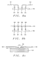
- FIG. 8 shows further details of the construction of the probes used to test the BGA devices contained within the BGA device strip of the present invention.
- FIG. 8 a shows probes 82 that contact the balls 84 of the BGA device that is contained within the BGA package 86 . Probes 82 approach the device balls under an angle, spring contact is in this manner established between the tester probes and the contact balls of the BGA device.
- FIG. 8 b shows another approach in the construction of the test probes.
- Probes 88 approach the contact balls of the BGA device in a direction that is perpendicular to the plane of the contact balls, probes 88 can be hollow in design whereby inside the body of the probe a spring (not shown) can be mounted that urges the head of the probe toward the balls 84 of the BGA device.
- the plane 90 represents a means of mounting the test probes and can, for instance, be a printed circuit board wherein further wiring is provided that forms part of the testing circuitry for the BGA devices under test.
- FIG. 8 c shows yet another approach to the construction of the test probes.
- a BGA device strip carrier 92 contains the BGA device that is to be tested (not shown).
- a docking plate 98 holds a prober card 96 into which the test probes 94 are mounted.
- the BGA device strip carrier is shown as being positioned on top of the heater table 100 .
Landscapes
- Engineering & Computer Science (AREA)
- Computer Hardware Design (AREA)
- Microelectronics & Electronic Packaging (AREA)
- General Engineering & Computer Science (AREA)
- Physics & Mathematics (AREA)
- General Physics & Mathematics (AREA)
- Testing Of Individual Semiconductor Devices (AREA)
- Testing Or Measuring Of Semiconductors Or The Like (AREA)
Abstract
Description
Claims (14)
Priority Applications (1)
| Application Number | Priority Date | Filing Date | Title |
|---|---|---|---|
| US10/140,572 US6535004B2 (en) | 1999-02-18 | 2002-05-08 | Testing of BGA and other CSP packages using probing techniques |
Applications Claiming Priority (2)
| Application Number | Priority Date | Filing Date | Title |
|---|---|---|---|
| US09/252,629 US6404212B1 (en) | 1999-02-18 | 1999-02-18 | Testing of BGA and other CSP packages using probing techniques |
| US10/140,572 US6535004B2 (en) | 1999-02-18 | 2002-05-08 | Testing of BGA and other CSP packages using probing techniques |
Related Parent Applications (1)
| Application Number | Title | Priority Date | Filing Date |
|---|---|---|---|
| US09/252,629 Division US6404212B1 (en) | 1999-02-18 | 1999-02-18 | Testing of BGA and other CSP packages using probing techniques |
Publications (2)
| Publication Number | Publication Date |
|---|---|
| US20020125908A1 US20020125908A1 (en) | 2002-09-12 |
| US6535004B2 true US6535004B2 (en) | 2003-03-18 |
Family
ID=22956850
Family Applications (3)
| Application Number | Title | Priority Date | Filing Date |
|---|---|---|---|
| US09/252,629 Expired - Lifetime US6404212B1 (en) | 1999-02-18 | 1999-02-18 | Testing of BGA and other CSP packages using probing techniques |
| US10/140,573 Expired - Lifetime US6791346B2 (en) | 1999-02-18 | 2002-05-08 | Testing of BGA and other CSP packages using probing techniques |
| US10/140,572 Expired - Lifetime US6535004B2 (en) | 1999-02-18 | 2002-05-08 | Testing of BGA and other CSP packages using probing techniques |
Family Applications Before (2)
| Application Number | Title | Priority Date | Filing Date |
|---|---|---|---|
| US09/252,629 Expired - Lifetime US6404212B1 (en) | 1999-02-18 | 1999-02-18 | Testing of BGA and other CSP packages using probing techniques |
| US10/140,573 Expired - Lifetime US6791346B2 (en) | 1999-02-18 | 2002-05-08 | Testing of BGA and other CSP packages using probing techniques |
Country Status (2)
| Country | Link |
|---|---|
| US (3) | US6404212B1 (en) |
| SG (3) | SG120967A1 (en) |
Cited By (8)
| Publication number | Priority date | Publication date | Assignee | Title |
|---|---|---|---|---|
| US6674296B1 (en) * | 2002-02-28 | 2004-01-06 | Advanced Micro Devices, Inc. | Probe card measurement tool |
| US20050086037A1 (en) * | 2003-09-29 | 2005-04-21 | Pauley Robert S. | Memory device load simulator |
| US20050174139A1 (en) * | 2003-10-14 | 2005-08-11 | Mahendran Chidambaram | Apparatus for high speed probing of flat panel displays |
| US20050206396A1 (en) * | 2004-03-16 | 2005-09-22 | Haruhiko Yoshioka | Vacuum prober and vacuum probe method |
| US20080221712A1 (en) * | 2007-03-09 | 2008-09-11 | Johnson John C | Socket alignment mechanism and method of using same |
| US20080238460A1 (en) * | 2007-03-30 | 2008-10-02 | Lothar Kress | Accurate alignment of semiconductor devices and sockets |
| US20090045827A1 (en) * | 2007-08-17 | 2009-02-19 | Andrew Gangoso | Multi-Site Probe |
| US20140370821A1 (en) * | 2013-06-12 | 2014-12-18 | Apple Inc. | Methods and Apparatus for Testing Electronic Devices with Antenna Arrays |
Families Citing this family (12)
| Publication number | Priority date | Publication date | Assignee | Title |
|---|---|---|---|---|
| US6891392B2 (en) * | 2003-02-21 | 2005-05-10 | Lsi Logic Corporation | Substrate impedance measurement |
| US6946866B2 (en) * | 2003-05-30 | 2005-09-20 | Lsi Logic Corporation | Measurement of package interconnect impedance using tester and supporting tester |
| CN100362357C (en) * | 2004-04-01 | 2008-01-16 | 华硕电脑股份有限公司 | Probe inspection device |
| JP4413130B2 (en) * | 2004-11-29 | 2010-02-10 | Okiセミコンダクタ株式会社 | Semiconductor device inspection method using probe card and semiconductor device inspected by the inspection method |
| US7596456B2 (en) * | 2005-11-18 | 2009-09-29 | Texas Instruments Incorporated | Method and apparatus for cassette integrity testing using a wafer sorter |
| DE102006015363B4 (en) * | 2006-04-03 | 2009-04-16 | Multitest Elektronische Systeme Gmbh | Test device for testing electronic components |
| JP4539685B2 (en) * | 2007-06-22 | 2010-09-08 | セイコーエプソン株式会社 | Component conveyor and IC handler |
| JP2010016053A (en) * | 2008-07-01 | 2010-01-21 | Tokyo Electron Ltd | Transfer mechanism for target object to be inspected |
| US9234853B2 (en) * | 2012-06-08 | 2016-01-12 | Beijert Engineering | Probe apparatus |
| KR101439342B1 (en) * | 2013-04-18 | 2014-09-16 | 주식회사 아이에스시 | Probe member for pogo pin |
| WO2015070135A2 (en) * | 2013-11-11 | 2015-05-14 | Delta Design Inc. | Integrated testing and handling mechanism |
| US11448680B2 (en) | 2020-03-31 | 2022-09-20 | KYOCERA AVX Components Corporation | Screening method for electrolytic capacitors that maintains individual capacitor unit identity |
Citations (8)
| Publication number | Priority date | Publication date | Assignee | Title |
|---|---|---|---|---|
| US4038599A (en) * | 1974-12-30 | 1977-07-26 | International Business Machines Corporation | High density wafer contacting and test system |
| US4607525A (en) * | 1984-10-09 | 1986-08-26 | General Signal Corporation | Height measuring system |
| US5315237A (en) * | 1990-08-06 | 1994-05-24 | Tokyo Electron Limited | Touch sensor unit of prober for testing electric circuit and electric circuit testing apparatus using the touch sensor unit |
| US5550480A (en) * | 1994-07-05 | 1996-08-27 | Motorola, Inc. | Method and means for controlling movement of a chuck in a test apparatus |
| US5570033A (en) | 1995-07-20 | 1996-10-29 | Vlsi Technology, Inc. | Spring probe BGA (ball grid array) contactor with device stop and method therefor |
| US5574668A (en) | 1995-02-22 | 1996-11-12 | Beaty; Elwin M. | Apparatus and method for measuring ball grid arrays |
| US5721496A (en) | 1996-01-23 | 1998-02-24 | Micron Technology, Inc. | Method and apparatus for leak checking unpackaged semiconductor dice |
| US5729896A (en) | 1996-10-31 | 1998-03-24 | International Business Machines Corporation | Method for attaching a flip chip on flexible circuit carrier using chip with metallic cap on solder |
Family Cites Families (5)
| Publication number | Priority date | Publication date | Assignee | Title |
|---|---|---|---|---|
| US5290134A (en) * | 1991-12-03 | 1994-03-01 | Advantest Corporation | Pick and place for automatic test handler |
| JPH0669295A (en) * | 1992-08-17 | 1994-03-11 | Tokyo Electron Ltd | Probe system |
| US5510724A (en) * | 1993-05-31 | 1996-04-23 | Tokyo Electron Limited | Probe apparatus and burn-in apparatus |
| US5510723A (en) * | 1994-03-01 | 1996-04-23 | Micron Custom Manufacturing, Inc. Usa | Diced semiconductor device handler |
| JP3689215B2 (en) * | 1997-02-20 | 2005-08-31 | 株式会社ルネサステクノロジ | Transport device for semiconductor device testing |
-
1999
- 1999-02-18 US US09/252,629 patent/US6404212B1/en not_active Expired - Lifetime
- 1999-06-23 SG SG200307318A patent/SG120967A1/en unknown
- 1999-06-30 SG SG200307295-6A patent/SG135932A1/en unknown
- 1999-06-30 SG SG9903180A patent/SG102545A1/en unknown
-
2002
- 2002-05-08 US US10/140,573 patent/US6791346B2/en not_active Expired - Lifetime
- 2002-05-08 US US10/140,572 patent/US6535004B2/en not_active Expired - Lifetime
Patent Citations (8)
| Publication number | Priority date | Publication date | Assignee | Title |
|---|---|---|---|---|
| US4038599A (en) * | 1974-12-30 | 1977-07-26 | International Business Machines Corporation | High density wafer contacting and test system |
| US4607525A (en) * | 1984-10-09 | 1986-08-26 | General Signal Corporation | Height measuring system |
| US5315237A (en) * | 1990-08-06 | 1994-05-24 | Tokyo Electron Limited | Touch sensor unit of prober for testing electric circuit and electric circuit testing apparatus using the touch sensor unit |
| US5550480A (en) * | 1994-07-05 | 1996-08-27 | Motorola, Inc. | Method and means for controlling movement of a chuck in a test apparatus |
| US5574668A (en) | 1995-02-22 | 1996-11-12 | Beaty; Elwin M. | Apparatus and method for measuring ball grid arrays |
| US5570033A (en) | 1995-07-20 | 1996-10-29 | Vlsi Technology, Inc. | Spring probe BGA (ball grid array) contactor with device stop and method therefor |
| US5721496A (en) | 1996-01-23 | 1998-02-24 | Micron Technology, Inc. | Method and apparatus for leak checking unpackaged semiconductor dice |
| US5729896A (en) | 1996-10-31 | 1998-03-24 | International Business Machines Corporation | Method for attaching a flip chip on flexible circuit carrier using chip with metallic cap on solder |
Cited By (12)
| Publication number | Priority date | Publication date | Assignee | Title |
|---|---|---|---|---|
| US6674296B1 (en) * | 2002-02-28 | 2004-01-06 | Advanced Micro Devices, Inc. | Probe card measurement tool |
| US20050086037A1 (en) * | 2003-09-29 | 2005-04-21 | Pauley Robert S. | Memory device load simulator |
| US20050174139A1 (en) * | 2003-10-14 | 2005-08-11 | Mahendran Chidambaram | Apparatus for high speed probing of flat panel displays |
| US20050206396A1 (en) * | 2004-03-16 | 2005-09-22 | Haruhiko Yoshioka | Vacuum prober and vacuum probe method |
| US7221176B2 (en) * | 2004-03-16 | 2007-05-22 | Tokyo Electron Limited | Vacuum prober and vacuum probe method |
| US20080221712A1 (en) * | 2007-03-09 | 2008-09-11 | Johnson John C | Socket alignment mechanism and method of using same |
| US7715931B2 (en) | 2007-03-09 | 2010-05-11 | Intel Corporation | Socket alignment mechanism and method of using same |
| US20080238460A1 (en) * | 2007-03-30 | 2008-10-02 | Lothar Kress | Accurate alignment of semiconductor devices and sockets |
| US20090045827A1 (en) * | 2007-08-17 | 2009-02-19 | Andrew Gangoso | Multi-Site Probe |
| US7847568B2 (en) | 2007-08-17 | 2010-12-07 | Advanced Micro Devices, Inc. | Multi-site probe |
| US20140370821A1 (en) * | 2013-06-12 | 2014-12-18 | Apple Inc. | Methods and Apparatus for Testing Electronic Devices with Antenna Arrays |
| US9154972B2 (en) * | 2013-06-12 | 2015-10-06 | Apple Inc. | Methods and apparatus for testing electronic devices with antenna arrays |
Also Published As
| Publication number | Publication date |
|---|---|
| SG135932A1 (en) | 2007-10-29 |
| US6791346B2 (en) | 2004-09-14 |
| US6404212B1 (en) | 2002-06-11 |
| US20020125909A1 (en) | 2002-09-12 |
| US20020125908A1 (en) | 2002-09-12 |
| SG120967A1 (en) | 2006-04-26 |
| SG102545A1 (en) | 2004-03-26 |
Similar Documents
| Publication | Publication Date | Title |
|---|---|---|
| US6535004B2 (en) | Testing of BGA and other CSP packages using probing techniques | |
| KR100295376B1 (en) | Probes and testers with a compact interface for integrated wafers integrated in a vertical plane | |
| KR100196195B1 (en) | Probe card | |
| US5631573A (en) | Probe-type test handler | |
| KR100283856B1 (en) | Probe Device and Probe Card | |
| US6242933B1 (en) | Device probe socket forming part of a test head, interfacing between test head and a probe handler, used for device strip testing | |
| US5461327A (en) | Probe apparatus | |
| JP4331165B2 (en) | Electronic component testing equipment | |
| US5894217A (en) | Test handler having turn table | |
| JPH0567652A (en) | Probing deivce | |
| WO1991003742A1 (en) | Automatic smd tester | |
| JPWO2004106945A1 (en) | Electronic component testing equipment | |
| US6343503B1 (en) | Module appearance inspection apparatus | |
| JP4279413B2 (en) | Insert for electronic component testing equipment | |
| JP4222442B2 (en) | Insert for electronic component testing equipment | |
| JPH04330753A (en) | Semiconductor inspection device | |
| US5086270A (en) | Probe apparatus | |
| JPH0370900B2 (en) | ||
| US5113132A (en) | Probing method | |
| US6864697B1 (en) | Flip-over alignment station for probe needle adjustment | |
| EP0522572A1 (en) | Method and device for measuring a semiconductor element with bumps, and method and device for manufacturing a semiconductor device | |
| JPH04280445A (en) | Probing device and probe card | |
| JP3169900B2 (en) | Prober | |
| JP3303968B2 (en) | Wafer and contact positioning system | |
| JPH0541423A (en) | Probe apparatus |
Legal Events
| Date | Code | Title | Description |
|---|---|---|---|
| STCF | Information on status: patent grant |
Free format text: PATENTED CASE |
|
| FEPP | Fee payment procedure |
Free format text: PAYOR NUMBER ASSIGNED (ORIGINAL EVENT CODE: ASPN); ENTITY STATUS OF PATENT OWNER: LARGE ENTITY Free format text: PAYER NUMBER DE-ASSIGNED (ORIGINAL EVENT CODE: RMPN); ENTITY STATUS OF PATENT OWNER: LARGE ENTITY |
|
| FPAY | Fee payment |
Year of fee payment: 4 |
|
| FPAY | Fee payment |
Year of fee payment: 8 |
|
| FPAY | Fee payment |
Year of fee payment: 12 |
|
| AS | Assignment |
Owner name: CITICORP INTERNATIONAL LIMITED, AS COMMON SECURITY AGENT, HONG KONG Free format text: SECURITY INTEREST;ASSIGNORS:STATS CHIPPAC, INC.;STATS CHIPPAC LTD.;REEL/FRAME:036288/0748 Effective date: 20150806 Owner name: STATS CHIPPAC LTD., SINGAPORE Free format text: CHANGE OF NAME;ASSIGNOR:ST ASSEMBLY TEST SERVICES LTD.;REEL/FRAME:036286/0590 Effective date: 20040608 Owner name: CITICORP INTERNATIONAL LIMITED, AS COMMON SECURITY Free format text: SECURITY INTEREST;ASSIGNORS:STATS CHIPPAC, INC.;STATS CHIPPAC LTD.;REEL/FRAME:036288/0748 Effective date: 20150806 |
|
| AS | Assignment |
Owner name: STATS CHIPPAC PTE. LTE., SINGAPORE Free format text: CHANGE OF NAME;ASSIGNOR:STATS CHIPPAC LTD.;REEL/FRAME:038378/0360 Effective date: 20160329 |
|
| AS | Assignment |
Owner name: STATS CHIPPAC, INC., CALIFORNIA Free format text: RELEASE BY SECURED PARTY;ASSIGNOR:CITICORP INTERNATIONAL LIMITED, AS COMMON SECURITY AGENT;REEL/FRAME:052950/0497 Effective date: 20190503 Owner name: STATS CHIPPAC PTE. LTD. FORMERLY KNOWN AS STATS CHIPPAC LTD., SINGAPORE Free format text: RELEASE BY SECURED PARTY;ASSIGNOR:CITICORP INTERNATIONAL LIMITED, AS COMMON SECURITY AGENT;REEL/FRAME:052950/0497 Effective date: 20190503 |