[go: up one dir, main page]

US6449754B1 - Method of measuring the accuracy of parasitic capacitance extraction - Google Patents

Method of measuring the accuracy of parasitic capacitance extraction Download PDF

Info

Publication number
US6449754B1
US6449754B1 US09/534,280 US53428000A US6449754B1 US 6449754 B1 US6449754 B1 US 6449754B1 US 53428000 A US53428000 A US 53428000A US 6449754 B1 US6449754 B1 US 6449754B1
Authority
US
United States
Prior art keywords
capacitance
error
net
weight factor
parasitic capacitance
Prior art date
Legal status (The legal status is an assumption and is not a legal conclusion. Google has not performed a legal analysis and makes no representation as to the accuracy of the status listed.)
Expired - Lifetime
Application number
US09/534,280
Inventor
Eileen H. You
Weize Xie
John F. MacDonald
Current Assignee (The listed assignees may be inaccurate. Google has not performed a legal analysis and makes no representation or warranty as to the accuracy of the list.)
Oracle America Inc
Original Assignee
Sun Microsystems Inc
Priority date (The priority date is an assumption and is not a legal conclusion. Google has not performed a legal analysis and makes no representation as to the accuracy of the date listed.)
Filing date
Publication date
Application filed by Sun Microsystems Inc filed Critical Sun Microsystems Inc
Priority to US09/534,280 priority Critical patent/US6449754B1/en
Assigned to SUN MICROSYSTEMS, INC. reassignment SUN MICROSYSTEMS, INC. ASSIGNMENT OF ASSIGNORS INTEREST (SEE DOCUMENT FOR DETAILS). Assignors: MACDONALD, JOHN F., XIE, WEIZE, YOU, EILEEN H.
Application granted granted Critical
Publication of US6449754B1 publication Critical patent/US6449754B1/en
Assigned to Oracle America, Inc. reassignment Oracle America, Inc. MERGER AND CHANGE OF NAME (SEE DOCUMENT FOR DETAILS). Assignors: Oracle America, Inc., ORACLE USA, INC., SUN MICROSYSTEMS, INC.
Anticipated expiration legal-status Critical
Expired - Lifetime legal-status Critical Current

Links

Images

Classifications

    • GPHYSICS
    • G06COMPUTING OR CALCULATING; COUNTING
    • G06FELECTRIC DIGITAL DATA PROCESSING
    • G06F30/00Computer-aided design [CAD]
    • G06F30/30Circuit design
    • G06F30/36Circuit design at the analogue level
    • G06F30/367Design verification, e.g. using simulation, simulation program with integrated circuit emphasis [SPICE], direct methods or relaxation methods

Definitions

  • the invention is related to extracting parasitic capacitance of integrated circuit interconnects and, in particular, to a method of determining the accuracy of the extraction.
  • parasitic capacitance is the capacitance exerted on a circuit element such as an interconnect by the surrounding circuit elements.
  • 3-D field solvers are considered the most accurate of extraction tools because they calculate the actual lines of electromagnetic force induced by electric charges traveling through the interconnect to determine the interconnect parasitic capacitance.
  • 3-D field solvers are extremely slow due to the enormous amount of data they have to process.
  • preparing the input data for a 3-D field solver is a tedious and time-consuming task. Therefore, it is generally not cost-effective in terms of time and resources to use a 3-D field solver to compute the entire, full-chip interconnect parasitic capacitance of a multi-million transistor integrated circuit.
  • An alternative method is to estimate the full-chip interconnect parasitic capacitance using another software tool called a layout parameter extraction tool.
  • This tool also uses a 3-D field solver, but only for creating a lookup table of parasitic capacitance models based on the particular process technology used to fabricate the circuit.
  • the 3-D field solver calculates parasitic capacitance values based on layout parameters such as interconnect width, thickness, and proximity to other interconnects. These values are subsequently used to generate mathematical relationships or models for the parasitic capacitance based on the process technology.
  • the models are stored in a lookup table along with the corresponding layout parameters.
  • the tool then employs a pattern recognition algorithm to match the layout parameters of the circuit being designed with the parasitic capacitance models stored in the lookup table to generate the parasitic capacitance data for the circuit.
  • the first step in accuracy determination is to generate a library of interconnect structures representative of the structures of the circuit being designed. Known or “golden” data for these test structures are then obtained using a 3-D field solver. The extraction tool is then applied to each test structure using the parasitic capacitance model of the extraction tool. The resulting data is compared to the known data. Finally, the extraction tool is adjusted, or calibrated, to reduce any errors to within a certain, predefined tolerance level.
  • FIG. 1 is a schematic diagram of a section of an integrated circuit showing several nets.
  • Blocks A 1 and A 2 represent functional circuit elements such as a memory or a control unit and are connected by a signal-carrying or “switching” net, net N.
  • Net N in this example is the “net of interest,” that is, the net for which parasitic capacitance is to be extracted.
  • Three other switching nets, net , net , and net are on the same layer as, below, and above net N, respectively, and connect blocks B 1 to B 2 , B 3 to B 4 , and B 5 to B 6 , which blocks represent other functional circuit elements in the circuit.
  • switching nets other than the net of interest
  • these switching nets will henceforth be referred to generally as net , where i is any integer up to the number of switching nets having a capacitive influence on the net of interest.
  • a static or non-switching net, net G connects the grounds Vss and runs underneath net N.
  • C N C G + ⁇ i ⁇ ⁇ C i C ( 1 )
  • C G is a static or non-switching capacitance between net N and net G
  • i is an integer number representing the switching nets other than net N
  • C is a coupling capacitance between net N and net .
  • K C ⁇ i ⁇ ⁇ C i C G + ⁇ ⁇ C i C ( 3 )
  • the present invention is directed to a technique that defines an error in an extracted parasitic capacitance for a net of interest as a sum of the errors in the extracted values of the individual capacitance elements which make up the total parasitic capacitance, with the error of each element being influenced by a weight factor.
  • the capacitance element corresponding to the error having the highest weight factor will have the biggest impact on signal propagation delay.
  • the technique of the present invention defines the error in the extracted value of a crosstalk factor for the net of interest as a difference between the errors in the extracted values of the individual capacitance elements, with the error in each element being influenced by a weight factor.
  • the capacitance element corresponding to the error having the highest weight factor will have the biggest impact on crosstalk.
  • the invention is related to a method of increasing the accuracy of an interconnect parasitic capacitance extraction tool.
  • the method includes the steps of extracting a parasitic capacitance of a net of interest with the extraction tool, calculating the error between the extracted parasitic capacitance and a known parasitic capacitance, applying a weight factor to the error to produce a weighted error, and selectively adjusting the extraction tool based on the weighted error.
  • the invention is related to a computer for extracting a parasitic capacitance of an integrated circuit interconnect.
  • the computer includes a microprocessor and a storage medium.
  • the storage medium stores computer-readable instructions for instructing the microprocessor to extract a parasitic capacitance of a net of interest, calculate an error between the extracted parasitic capacitance and a known parasitic capacitance, apply a weight factor to the error to produce a weighted error, and selectively adjust an extraction tool based on the weighted error.
  • the invention is related to a method of designing an integrated circuit.
  • the method includes defining the specifications for the integrated circuit, laying out the various circuit elements, and verifying the accuracy of the interconnect parasitic capacitance extraction tool. Verifying the accuracy of the extraction tool includes extracting a parasitic capacitance for a net of interest in the integrated circuit, calculating an error between the extracted parasitic capacitance and a known parasitic capacitance of the net of interest, applying a weight factor to the error to produce a weighted error, and selectively adjusting the extraction tool based on the weighted error.
  • the adjusted extraction tool is used to extract the full-chip parasitic capacitance, and the integrated circuit is computer simulated using the extracted parasitic capacitance.
  • the invention is related to a method of determining the accuracy of an interconnect parasitic capacitance extraction tool.
  • the method includes extracting a static capacitance and a coupling capacitance of a net of interest with the extraction tool, calculating a static capacitance error between the extracted static capacitance and a known static capacitance of the net of interest, calculating a coupling capacitance error between the extracted coupling capacitance and a known coupling capacitance, applying a static capacitance weight factor to the static capacitance error to produce a weighted static capacitance error, applying a coupling capacitance weight factor to the coupling capacitance error to produce a weighted coupling capacitance error, and selectively adjusting the extraction tool based on the weighted static capacitance error and the weighted coupling capacitance error.
  • the invention is related to a method of determining the accuracy of an interconnect parasitic capacitance extraction tool.
  • the method includes extracting a coupling capacitance and a net capacitance of a net of interest with the extraction tool, calculating a coupling capacitance error between the extracted coupling capacitance and a known coupling capacitance of the net of interest, and calculating a net capacitance error between the extracted net capacitance and a known net capacitance, applying a coupling capacitance weight factor to the coupling capacitance error to produce a weighted coupling capacitance error, applying a net capacitance weight factor to the net capacitance error to produce a weighted net capacitance error, and selectively adjusting the extraction tool based on the weighted coupling capacitance error and the weighted net capacitance error.
  • An advantage of the present invention is circuit designers can focus calibration of their extraction tool on the capacitance element with the highest weight factor.
  • FIG. 1 is a schematic diagram showing a section of a circuit having several nets.
  • FIG. 2 is a flowchart of an accuracy determination operation in accordance with an embodiment of the extraction tool of the present invention.
  • FIG. 3 is a schematic diagram showing a computer for running the extraction tool of the present invention.
  • FIG. 4 is a flowchart of a design process using the extraction tool of the present invention.
  • M is a Miller effect scaling factor.
  • M is a Miller effect scaling factor.
  • M is known to one having ordinary skill in the art and will not be discussed here except to say it ranges from 0-2, depending on the extent of the switching activity of net C.
  • ⁇ T C T - C ⁇ T C ⁇ T ( 6 )
  • Equations (7)-(9) can then be substituted into equation (5) to obtain the following equation:
  • C ⁇ T ⁇ ( 1 + ⁇ T ) C ⁇ G ⁇ ( 1 + ⁇ G ) + ⁇ i ⁇ ⁇ M i ⁇ C ⁇ i C ⁇ ( 1 + ⁇ i C ) ( 10 )
  • C T C ⁇ G + ⁇ i ⁇ ⁇ M i ⁇ C ⁇ i C ( 12 )
  • ⁇ T ⁇ G ⁇ C ⁇ G C ⁇ T + ⁇ i ⁇ ⁇ M i ⁇ ⁇ i C ⁇ C ⁇ i C C ⁇ T ( 14 )
  • equation (14) One advantage of equation (14) is the weight factors allow circuit designers to focus calibration of the extraction tool on either the coupling capacitance error C or the static capacitance error ⁇ G , whichever has the higher weight factor. Another advantage is the weight factors are composed of known or golden values, thus assuring the accuracy of the weight factors.
  • K C can be written as:
  • Equation (16) ⁇ i ⁇ ⁇ C ⁇ i C ⁇ ( 1 + ⁇ i C ) C N ( 17 )
  • the crosstalk factor error ⁇ K equals the difference between the coupling capacitance error C and the net capacitance error ⁇ N , with each error term being influenced by a weight factor.
  • each error C is multiplied by a known ratio C ⁇ i C / ( ⁇ i ⁇ ⁇ C ⁇ i C ) ⁇
  • this error is multiplied by ( 1 + ⁇ i ⁇ ⁇ C ⁇ i C ⁇ ⁇ i C / ⁇ i ⁇ ⁇ C ⁇ i C ) ⁇
  • the error determination operation of the present invention begins by receiving and processing layout and parametric data for a predetermined test circuit (ST 21 ). Then a static capacitance C G is extracted and the error ⁇ G in the extracted value is calculated (ST 22 ). The coupling capacitance C is then extracted and the error C is calculated (ST 23 ) for each switching net i. Using this data, a total capacitance error ⁇ T (ST 24 ) and a crosstalk factor error ⁇ K (ST 25 ) for the net of interest is calculated. These calculations are repeated in turn until all nets of interest for the test circuit have been extracted (ST 26 ). The resulting data are then stored, usually in matrix form, for circuit designers to access and evaluate.
  • the accuracy definition in the present invention may be stored and executed by a computer such as the one schematically depicted in FIG. 3 .
  • the computer 30 comprises, among other things, a microprocessor 32 , a storage medium 34 , a display unit 36 , and a keyboard 38 .
  • the storage medium 34 stores the extraction tool as computer-readable instructions for instructing the microprocessor 32 to execute the steps generally shown in FIG. 2 .
  • the display unit 36 visually displays data produced by the microprocessor 32
  • the keyboard 38 allows a user to manually input data into the microprocessor 32 .
  • the computer 30 of FIG. 3 can be used to aid the design process generally shown in the flowchart of FIG. 4 .
  • the first step in the design process is to define the circuit specifications and parameters including functionality, features, speed, power consumption, and size (ST 41 ).
  • the various circuit elements for example, clock generator, memory, and controller, must be laid out and arranged within the allotted die or chip area (ST 42 ).
  • the accuracy of the extraction tool stored on the computer 30 is verified in the manner previously described and shown in FIG. 2 (ST 43 ).
  • the tool is used to extract the full-chip parasitic capacitance of the integrated circuit (ST 44 ).
  • a simulation of the entire circuit is then performed (ST 45 ) including timing and crosstalk analyses. After the simulation is successfully completed, the design may be released to the wafer fab to begin volume production.

Landscapes

  • Engineering & Computer Science (AREA)
  • Computer Hardware Design (AREA)
  • Physics & Mathematics (AREA)
  • Theoretical Computer Science (AREA)
  • Microelectronics & Electronic Packaging (AREA)
  • Evolutionary Computation (AREA)
  • Geometry (AREA)
  • General Engineering & Computer Science (AREA)
  • General Physics & Mathematics (AREA)
  • Design And Manufacture Of Integrated Circuits (AREA)

Abstract

A technique measuring accuracy of parasitic capacitance extraction defines the error in an extracted total net parasitic capacitance intended for timing analysis as a sum of the errors in the extracted values of the individual capacitance elements, with the error for each element being influenced by a weight factor. Similarly, the technique defines an error in the extracted value of a crosstalk factor for the net of interest as a difference between the errors in the extracted values of the individual capacitance elements, with the error in each element being influenced by a weight factor. For signal timing and crosstalk analyses, the weight factors allow a designer to focus calibration of the extraction tool on the capacitive element having the highest weight factor.

Description

The invention is related to extracting parasitic capacitance of integrated circuit interconnects and, in particular, to a method of determining the accuracy of the extraction.
BACKGROUND OF THE INVENTION
The speed at which signals propagate along an interconnection line, or interconnect, within an integrated circuit can be limited by the parasitic capacitance associated with the interconnect. In general, parasitic capacitance is the capacitance exerted on a circuit element such as an interconnect by the surrounding circuit elements. As semiconductor fabrication processes and design geometries shrink toward deep and ultra-deep submicron levels, the effect of interconnect parasitic capacitance on signal propagation becomes more pronounced. Therefore, a vital part of the integrated circuit design process is being able to accurately determine, or extract, parasitic capacitance.
One method of determining interconnect parasitic capacitance is by using a software tool called a 3-D field solver. 3-D field solvers are considered the most accurate of extraction tools because they calculate the actual lines of electromagnetic force induced by electric charges traveling through the interconnect to determine the interconnect parasitic capacitance. However, for an integrated circuit containing millions of transistors and interconnects, 3-D field solvers are extremely slow due to the enormous amount of data they have to process. In addition, preparing the input data for a 3-D field solver is a tedious and time-consuming task. Therefore, it is generally not cost-effective in terms of time and resources to use a 3-D field solver to compute the entire, full-chip interconnect parasitic capacitance of a multi-million transistor integrated circuit.
An alternative method is to estimate the full-chip interconnect parasitic capacitance using another software tool called a layout parameter extraction tool. This tool also uses a 3-D field solver, but only for creating a lookup table of parasitic capacitance models based on the particular process technology used to fabricate the circuit. The 3-D field solver calculates parasitic capacitance values based on layout parameters such as interconnect width, thickness, and proximity to other interconnects. These values are subsequently used to generate mathematical relationships or models for the parasitic capacitance based on the process technology. The models are stored in a lookup table along with the corresponding layout parameters. The tool then employs a pattern recognition algorithm to match the layout parameters of the circuit being designed with the parasitic capacitance models stored in the lookup table to generate the parasitic capacitance data for the circuit.
Tools for extracting interconnect parasitic capacitance are available to one of ordinary skill in the art such as StarRC™ from Avant! Corporation (http://www.avanticorp.com) and Fire & Ice™ from Simplex Solutions, Inc. (http://www.simplex.com).
Regardless of which tool is used, it is important to determine the accuracy of the data generated. The first step in accuracy determination is to generate a library of interconnect structures representative of the structures of the circuit being designed. Known or “golden” data for these test structures are then obtained using a 3-D field solver. The extraction tool is then applied to each test structure using the parasitic capacitance model of the extraction tool. The resulting data is compared to the known data. Finally, the extraction tool is adjusted, or calibrated, to reduce any errors to within a certain, predefined tolerance level.
In general, parasitic capacitance is determined relative to a signal path or “net,” which is one or more interconnects electrically linked together. FIG. 1 is a schematic diagram of a section of an integrated circuit showing several nets. Blocks A1 and A2 represent functional circuit elements such as a memory or a control unit and are connected by a signal-carrying or “switching” net, net N. Net N in this example is the “net of interest,” that is, the net for which parasitic capacitance is to be extracted. Three other switching nets, net , net , and net are on the same layer as, below, and above net N, respectively, and connect blocks B1 to B2, B3 to B4, and B5 to B6, which blocks represent other functional circuit elements in the circuit. Although three switching nets (other than the net of interest) are shown here, there may of course be more or less than three, depending on the type of circuit. For simplicity, these switching nets will henceforth be referred to generally as net , where i is any integer up to the number of switching nets having a capacitive influence on the net of interest. A static or non-switching net, net G, connects the grounds Vss and runs underneath net N.
Traditional extraction methods define the net capacitance CN of net N as: C N = C G + i C i C ( 1 )
Figure US06449754-20020910-M00001
where CG is a static or non-switching capacitance between net N and net G, i is an integer number representing the switching nets other than net N, and C is a coupling capacitance between net N and net . Also, an error δN between the extracted value of the net capacitance CN and a known or golden value {tilde over (C)}N is traditionally defined as: δ N = C N - C ~ N C ~ N ( 2 )
Figure US06449754-20020910-M00002
However, for deep and ultra-deep submicron integrated circuits, the traditional net capacitance CN is not directly used in signal timing analysis.
Similarly, referring still to FIG. 1, for crosstalk noise analysis, traditional extraction methods define a crosstalk factor KC representing the crosstalk between net N and the other switching nets as: K C = i C i C C G + C i C ( 3 )
Figure US06449754-20020910-M00003
The crosstalk factor error δK in the extracted value of the crosstalk factor KC,like the error δN of equation (2), is traditionally defined as: δ K = K C - K ~ C K ~ C ( 4 )
Figure US06449754-20020910-M00004
where {tilde over (K)}C is a known crosstalk factor for the given circuit.
SUMMARY OF THE INVENTION
The present invention is directed to a technique that defines an error in an extracted parasitic capacitance for a net of interest as a sum of the errors in the extracted values of the individual capacitance elements which make up the total parasitic capacitance, with the error of each element being influenced by a weight factor. For purposes of signal timing analysis, the capacitance element corresponding to the error having the highest weight factor will have the biggest impact on signal propagation delay.
Similarly, the technique of the present invention defines the error in the extracted value of a crosstalk factor for the net of interest as a difference between the errors in the extracted values of the individual capacitance elements, with the error in each element being influenced by a weight factor. For purposes of crosstalk analysis, the capacitance element corresponding to the error having the highest weight factor will have the biggest impact on crosstalk.
In one embodiment, the invention is related to a method of increasing the accuracy of an interconnect parasitic capacitance extraction tool. The method includes the steps of extracting a parasitic capacitance of a net of interest with the extraction tool, calculating the error between the extracted parasitic capacitance and a known parasitic capacitance, applying a weight factor to the error to produce a weighted error, and selectively adjusting the extraction tool based on the weighted error.
In one embodiment, the invention is related to a computer for extracting a parasitic capacitance of an integrated circuit interconnect. The computer includes a microprocessor and a storage medium. The storage medium stores computer-readable instructions for instructing the microprocessor to extract a parasitic capacitance of a net of interest, calculate an error between the extracted parasitic capacitance and a known parasitic capacitance, apply a weight factor to the error to produce a weighted error, and selectively adjust an extraction tool based on the weighted error.
In one embodiment, the invention is related to a method of designing an integrated circuit. The method includes defining the specifications for the integrated circuit, laying out the various circuit elements, and verifying the accuracy of the interconnect parasitic capacitance extraction tool. Verifying the accuracy of the extraction tool includes extracting a parasitic capacitance for a net of interest in the integrated circuit, calculating an error between the extracted parasitic capacitance and a known parasitic capacitance of the net of interest, applying a weight factor to the error to produce a weighted error, and selectively adjusting the extraction tool based on the weighted error. The adjusted extraction tool is used to extract the full-chip parasitic capacitance, and the integrated circuit is computer simulated using the extracted parasitic capacitance.
In one embodiment, the invention is related to a method of determining the accuracy of an interconnect parasitic capacitance extraction tool. The method includes extracting a static capacitance and a coupling capacitance of a net of interest with the extraction tool, calculating a static capacitance error between the extracted static capacitance and a known static capacitance of the net of interest, calculating a coupling capacitance error between the extracted coupling capacitance and a known coupling capacitance, applying a static capacitance weight factor to the static capacitance error to produce a weighted static capacitance error, applying a coupling capacitance weight factor to the coupling capacitance error to produce a weighted coupling capacitance error, and selectively adjusting the extraction tool based on the weighted static capacitance error and the weighted coupling capacitance error.
In one embodiment, the invention is related to a method of determining the accuracy of an interconnect parasitic capacitance extraction tool. The method includes extracting a coupling capacitance and a net capacitance of a net of interest with the extraction tool, calculating a coupling capacitance error between the extracted coupling capacitance and a known coupling capacitance of the net of interest, and calculating a net capacitance error between the extracted net capacitance and a known net capacitance, applying a coupling capacitance weight factor to the coupling capacitance error to produce a weighted coupling capacitance error, applying a net capacitance weight factor to the net capacitance error to produce a weighted net capacitance error, and selectively adjusting the extraction tool based on the weighted coupling capacitance error and the weighted net capacitance error.
An advantage of the present invention is circuit designers can focus calibration of their extraction tool on the capacitance element with the highest weight factor. Other advantages will become apparent from the following description and from the claims.
DESCRIPTION OF THE DRAWINGS
FIG. 1 is a schematic diagram showing a section of a circuit having several nets.
FIG. 2 is a flowchart of an accuracy determination operation in accordance with an embodiment of the extraction tool of the present invention.
FIG. 3 is a schematic diagram showing a computer for running the extraction tool of the present invention.
FIG. 4 is a flowchart of a design process using the extraction tool of the present invention.
DETAILED DESCRIPTION OF THE PREFERRED EMBODIMENTS
Reference is again made to the circuit section of FIG. 1 and the net of interest, net N, shown therein. For signal timing analysis of deep and ultra-deep submicron integrated circuits, it is more useful to define a total capacitance CT for net N. For the purpose of static timing analysis of the present invention, the total capacitance CT is defined as: C T = C G + i M i · C i C ( 5 )
Figure US06449754-20020910-M00005
where M is a Miller effect scaling factor. Use of the Miller effect scaling factor M is known to one having ordinary skill in the art and will not be discussed here except to say it ranges from 0-2, depending on the extent of the switching activity of net C.
The error δT between the extracted value of total capacitance CT of net N and the known value {tilde over (C)}T can be defined as: δ T = C T - C ~ T C ~ T ( 6 )
Figure US06449754-20020910-M00006
From equation (6), the total capacitance CT can be written as:
C T ={tilde over (C)} T(1+δT)  (7)
Similarly, the static and coupling capacitance CG and C can also be written as:
C G ={tilde over (C)} G(1+δG)  (8)
C=C(1+C)  (9)
Equations (7)-(9) can then be substituted into equation (5) to obtain the following equation: C ~ T ( 1 + δ T ) = C ~ G ( 1 + δ G ) + i M i · C ~ i C ( 1 + δ i C ) ( 10 )
Figure US06449754-20020910-M00007
Expanding equation (10) results in the following equation: C ~ T + C ~ T · δ T = C ~ G + C ~ G · δ G + i M i · C ~ i C + i M i · C ~ i C · δ i C ( 11 )
Figure US06449754-20020910-M00008
Then, it follows from equation (5) that CT can be written as: C ~ T = C ~ G + i M i · C ~ i C ( 12 )
Figure US06449754-20020910-M00009
Substituting equation (12) into the right side of equation (9) and canceling like terms results in the following equations:
{tilde over (C)} T·δT ={tilde over (C)} G·δG+Σ·C·C  (13)
and δ T = δ G · C ~ G C ~ T + i M i · δ i C · C ~ i C C ~ T ( 14 )
Figure US06449754-20020910-M00010
From equation (14), it can be seen the error δT in the total capacitance CT of net N equals the sum of the static capacitance error δG and the coupling capacitance error C, with each error term being influenced by a weight factor. In the case of the static capacitance error δG, this error is multiplied by a ratio of the known static capacitance over the known total capacitance, {tilde over (C)}G/{tilde over (C)}T. In the case of the coupling capacitance error C, each error C is multiplied a known weight factor i M i · C - i c / C ~ T ·
Figure US06449754-20020910-M00011
One advantage of equation (14) is the weight factors allow circuit designers to focus calibration of the extraction tool on either the coupling capacitance error C or the static capacitance error δG, whichever has the higher weight factor. Another advantage is the weight factors are composed of known or golden values, thus assuring the accuracy of the weight factors.
Because a typical circuit has an enormous number of switching nets and the parasitic capacitance for each net must be extracted, and the errors for the nets of interest in an error matrix ΔT, where each element of the matrix holds an error δT for each net of interest. The accuracy of the extraction tool can then be ascertained by an appropriate evaluation of the entire error matrix ΔT .
The definition of parasitic extraction accuracy in the present invention thus far has been with reference to signal timing analysis. Following now is a description of the technique with reference to crosstalk noise analysis.
Referring still to FIG. 1 and substituting equation (1) into equation (3) from above, the crosstalk factor KC can be written as: K C = i C i C C N ( 15 )
Figure US06449754-20020910-M00012
Also, by rearranging equation (4), KC can be written as:
K C ={tilde over (K)} C(1+δK)  (16)
Substituting equation (16) and equation (7) (shown above) into equation (15) results in the following equation: K ~ C ( 1 + δ K ) = i C ~ i C ( 1 + δ i C ) C N ( 17 )
Figure US06449754-20020910-M00013
Referring again to equation (15), it follows that the known crosstalk factor {tilde over (K)}C can be written as: K ~ C = i C ~ i C C ~ N ( 18 )
Figure US06449754-20020910-M00014
Also, by rearranging equation (2), CN can be written as:
C N ={tilde over (C)} N(1+δN)  (19)
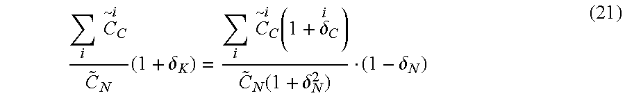
Substituting equations (18) and (19) into equation (17) results in the following equation: i C ~ i C C ~ N ( 1 + δ K ) = i C ~ i C ( 1 + δ i C ) C ~ N ( 1 + δ N ) ( 20 )
Figure US06449754-20020910-M00015
Next, the righthand side of equation (20) is multiplied by (1−δN)/(1−δN) to obtain the following equation: i C ~ i C C ~ N ( 1 + δ K ) = i C ~ i C ( 1 + δ i C ) C ~ N ( 1 + δ N 2 ) · ( 1 - δ N ) ( 21 )
Figure US06449754-20020910-M00016
For any extraction tool to be useful, δN must be much less than 1 (δN<<1). Therefore, equation (21) can be written as: i C ~ i C C ~ N ( 1 + δ K ) = i C ~ i C ( 1 + δ i C ) C ~ N · ( 1 - δ N ) ( 22 )
Figure US06449754-20020910-M00017
Expanding and canceling like terms, equation (22) can be written as: i C ~ i C + i C ~ i C · δ K = i C ~ i C + i C ~ i C · δ i C - δ N · i C ~ i C - δ N · i C ~ i C · δ i C ( 23 )
Figure US06449754-20020910-M00018
Solving equation (23) for δK results in the following equation: δ K = i C ~ i C · δ i C i C ~ i C - ( 1 + i C ~ i C · δ i C i C ~ i C ) δ N ( 24 )
Figure US06449754-20020910-M00019
As can be seen from equation (24), the crosstalk factor error δK equals the difference between the coupling capacitance error C and the net capacitance error δN, with each error term being influenced by a weight factor. In the case of the coupling capacitance error C, each error C is multiplied by a known ratio C ~ i C / ( i C ~ i C ) ·
Figure US06449754-20020910-M00020
In the case of the net capacitance error δN, this error is multiplied by ( 1 + i C ~ i C · δ i C / i C ~ i C ) ·
Figure US06449754-20020910-M00021
Referring now to FIG. 2, the error determination operation of the present invention begins by receiving and processing layout and parametric data for a predetermined test circuit (ST21). Then a static capacitance CG is extracted and the error δG in the extracted value is calculated (ST22). The coupling capacitance C is then extracted and the error C is calculated (ST23) for each switching net i. Using this data, a total capacitance error δT (ST24) and a crosstalk factor error δK (ST25) for the net of interest is calculated. These calculations are repeated in turn until all nets of interest for the test circuit have been extracted (ST26). The resulting data are then stored, usually in matrix form, for circuit designers to access and evaluate.
In some embodiments, the accuracy definition in the present invention may be stored and executed by a computer such as the one schematically depicted in FIG. 3. The computer 30 comprises, among other things, a microprocessor 32, a storage medium 34, a display unit 36, and a keyboard 38. The storage medium 34 stores the extraction tool as computer-readable instructions for instructing the microprocessor 32 to execute the steps generally shown in FIG. 2. The display unit 36 visually displays data produced by the microprocessor 32, and the keyboard 38 allows a user to manually input data into the microprocessor 32.
In some embodiments, the computer 30 of FIG. 3 can be used to aid the design process generally shown in the flowchart of FIG. 4. The first step in the design process is to define the circuit specifications and parameters including functionality, features, speed, power consumption, and size (ST41). Next, the various circuit elements, for example, clock generator, memory, and controller, must be laid out and arranged within the allotted die or chip area (ST42). Once this is done, the accuracy of the extraction tool stored on the computer 30 is verified in the manner previously described and shown in FIG. 2 (ST43). Once the accuracy of the tool has been verified to within a certain, predefined level, the tool is used to extract the full-chip parasitic capacitance of the integrated circuit (ST44). A simulation of the entire circuit is then performed (ST45) including timing and crosstalk analyses. After the simulation is successfully completed, the design may be released to the wafer fab to begin volume production.
It is to be understood the embodiments described herein are illustrative only, and other embodiments may be derived by one having ordinary skill in the art without departing from the scope of the invention. Accordingly, the scope of the invention should be limited only by the following claims.

Claims (23)

What is claimed is:
1. A method of increasing an accuracy of an interconnect parasitic capacitance extraction tool, comprising:
extracting a parasitic capacitance for a net of interest with the extraction tool;
calculating an error between the extracted parasitic capacitance and a known parasitic capacitance of the net of interest;
applying a weight factor to the error to produce a weighted error; and
selectively adjusting the extraction tool based on the weighted error.
2. The method of claim 1, wherein the extraction tool is adjusted by the weight factor.
3. The method of claim 1, wherein the extracted parasitic capacitance is a static capacitance.
4. The method of claim 1, wherein the extracted parasitic capacitance is a coupling capacitance.
5. The method of claim 1, wherein the error is equal to the extracted parasitic capacitance minus the known parasitic capacitance, divided by the known parasitic capacitance.
6. The method of claim 1, wherein the weight factor is equal to a known static capacitance divided by a known total capacitance.
7. The method of claim 1, wherein the weight factor is equal to a known coupling capacitance divided by a known total capacitance.
8. The method of claim 7, wherein the weight factor is multiplied by a Miller factor.
9. The method of claim 1, wherein the weight factor is equal to A divided by B, wherein A is a product of a known coupling capacitance and a coupling capacitance error, and wherein B is the known coupling capacitance.
10. The method of claim 1, wherein the weight factor is equal to 1+A/B, wherein A is a product of a known coupling capacitance and a coupling capacitance error, and wherein B is the known coupling capacitance.
11. A computer for extracting a parasitic capacitance of an integrated circuit interconnect, comprising:
a microprocessor; and
a storage medium storing computer-readable instructions for instructing the microprocessor to:
(a) extract a parasitic capacitance of a net of interest;
(b) calculate an error between the extracted parasitic capacitance and a known parasitic capacitance of the net of interest;
(c) apply a weight factor to the error to produce a weighted error; and
(d) selectively adjust an extraction tool based on the weighted error.
12. The computer of claim 11, wherein the extraction tool is adjusted by the weight factor.
13. The computer of claim 11, wherein the extracted parasitic capacitance is a static capacitance.
14. The computer of claim 11, wherein the extracted parasitic capacitance is a coupling capacitance.
15. The computer of claim 11, wherein the error is equal to the extracted parasitic capacitance minus the known parasitic capacitance, divided by the known parasitic capacitance.
16. The computer of claim 11, wherein the weight factor is equal to a known static capacitance divided by a known total capacitance.
17. The computer of claim 11, wherein the weight factor is equal to a known coupling capacitance divided by a known total capacitance.
18. The computer of claim 17, wherein the weight factor is multiplied by a Miller factor.
19. The computer of claim 11, wherein the weight factor is equal to A divided by B, wherein A is a product of a known coupling capacitance and a coupling capacitance error, and wherein B is the known coupling capacitance.
20. The computer of claim 11, wherein the weight factor is equal to 1+A/B, wherein A is a product of a known coupling capacitance and a coupling capacitance error, and wherein B is the known coupling capacitance.
21. A method of designing an integrated circuit, comprising:
defining specifications for the integrated circuit;
laying out circuit elements;
verifying an accuracy of an interconnect parasitic capacitance extraction tool, including:
(a) extracting a parasitic capacitance for a net of interest in the integrated circuit using the extraction tool;
(b) calculating an error between the extracted parasitic capacitance and a known parasitic capacitance of the net of interest;
(c) applying a weight factor to the error to produce a weighted error; and
(d) adjusting the extraction tool based on the weighted error;
extracting a full-chip parasitic capacitance for the integrated circuit using the adjusted extraction tool; and
computer simulating the integrated circuit using the extracted parasitic capacitance.
22. A method of increasing an accuracy of an interconnect parasitic capacitance extraction tool, comprising:
extracting a static capacitance and a coupling capacitance of a net of interest with the extraction tool;
calculating a static capacitance error between the extracted static capacitance and a known static capacitance of the net of interest;
calculating a coupling capacitance error between the extracted coupling capacitance and a known coupling capacitance of the net of interest;
applying a static capacitance weight factor to the static capacitance error to produce a weighted static capacitance error;
applying a coupling capacitance weight factor to the coupling capacitance error to produce a weighted coupling capacitance error; and
selectively adjusting the extraction tool based on the weighted static capacitance error and weighted coupling capacitance error.
23. A method of increasing an accuracy of an interconnect parasitic capacitance extraction tool, comprising:
extracting a coupling capacitance and a net capacitance of a net of interest with the extraction tool;
calculating a coupling capacitance error between the extracted coupling capacitance and a known coupling capacitance of the net of interest;
calculating a net capacitance error between the extracted net capacitance and a known net capacitance of the net of interest;
applying a coupling capacitance weight factor to the coupling capacitance error to produce a weighted coupling capacitance error;
applying a net capacitance weight factor to the net capacitance error to produce a weighted net capacitance error; and
selectively adjusting the extraction tool based on the weighted coupling capacitance error and weighted net capacitance error.
US09/534,280 2000-03-24 2000-03-24 Method of measuring the accuracy of parasitic capacitance extraction Expired - Lifetime US6449754B1 (en)

Priority Applications (1)

Application Number Priority Date Filing Date Title
US09/534,280 US6449754B1 (en) 2000-03-24 2000-03-24 Method of measuring the accuracy of parasitic capacitance extraction

Applications Claiming Priority (1)

Application Number Priority Date Filing Date Title
US09/534,280 US6449754B1 (en) 2000-03-24 2000-03-24 Method of measuring the accuracy of parasitic capacitance extraction

Publications (1)

Publication Number Publication Date
US6449754B1 true US6449754B1 (en) 2002-09-10

Family

ID=24129420

Family Applications (1)

Application Number Title Priority Date Filing Date
US09/534,280 Expired - Lifetime US6449754B1 (en) 2000-03-24 2000-03-24 Method of measuring the accuracy of parasitic capacitance extraction

Country Status (1)

Country Link
US (1) US6449754B1 (en)

Cited By (10)

* Cited by examiner, † Cited by third party
Publication number Priority date Publication date Assignee Title
US20030122123A1 (en) * 2001-12-31 2003-07-03 Texas Instruments Incorporated Method and apparatus for determining parasitic capacitances in an integrated circuit
US20030237063A1 (en) * 2002-06-24 2003-12-25 Mentor Graphics Corporation Hierarchical feature extraction for electrical interaction calculations
US20040123257A1 (en) * 2002-12-20 2004-06-24 Taiwan Semiconductor Manufacturing Co., Ltd. Process related deviation corrected parasitic capacitance modeling method
US20050240883A1 (en) * 2004-04-22 2005-10-27 Ching-Chao Huang Fringe RLGC model for interconnect parasitic extraction
US20050243869A1 (en) * 2004-04-28 2005-11-03 International Business Machines Corporation Method of identifying paths with delays dominated by a particular factor
US20070198967A1 (en) * 2006-02-17 2007-08-23 Zhuoxiang Ren Computation of electrical properties of an ic layout
US20090199139A1 (en) * 2007-12-27 2009-08-06 David White Method, system, and computer program product for improved electrical analysis
US8224637B1 (en) * 2007-04-02 2012-07-17 Xilinx, Inc. Method and apparatus for modeling transistors in an integrated circuit design
US20120260225A1 (en) * 2007-06-29 2012-10-11 Taiwan Semiconductor Manufacturing Company, Ltd. Accurate Parasitic Capacitance Extraction for Ultra Large Scale Integrated Circuits
US20140071087A1 (en) * 2012-09-10 2014-03-13 Apple Inc. Determination and Reduction of Parasitic Capacitance Variation Due to Display Noise

Citations (9)

* Cited by examiner, † Cited by third party
Publication number Priority date Publication date Assignee Title
US5568395A (en) * 1994-06-29 1996-10-22 Lsi Logic Corporation Modeling and estimating crosstalk noise and detecting false logic
US5706206A (en) * 1995-12-01 1998-01-06 Hewlett-Packard Co. Method of extracting parasitic capacitance values from the physical design of an integrated circuit
US5896300A (en) * 1996-08-30 1999-04-20 Avant| Corporation Methods, apparatus and computer program products for performing post-layout verification of microelectronic circuits by filtering timing error bounds for layout critical nets
US5901063A (en) * 1997-02-21 1999-05-04 Frequency Technology, Inc. System and method for extracting parasitic impedance from an integrated circuit layout
US5923568A (en) 1997-03-31 1999-07-13 Hewlett-Packard Company Distributed capacitance estimations of interconnects within integrated circuits
US6068660A (en) * 1998-06-22 2000-05-30 International Business Machines Corporation Method and apparatus for determining parasitic capacitance
US6212492B1 (en) * 1996-08-07 2001-04-03 Nec Corporation Apparatus and method for circuit simulation which accounts for parasitic elements
US6243653B1 (en) * 1998-08-17 2001-06-05 Vlsi Technology, Inc. Methods and apparatus for extracting parasitic capacitance values from a physical design of an integrated circuit
US6321365B1 (en) * 1999-01-26 2001-11-20 Hewlett-Packard Company System and method for detecting storage nodes that are susceptible to charge sharing

Patent Citations (9)

* Cited by examiner, † Cited by third party
Publication number Priority date Publication date Assignee Title
US5568395A (en) * 1994-06-29 1996-10-22 Lsi Logic Corporation Modeling and estimating crosstalk noise and detecting false logic
US5706206A (en) * 1995-12-01 1998-01-06 Hewlett-Packard Co. Method of extracting parasitic capacitance values from the physical design of an integrated circuit
US6212492B1 (en) * 1996-08-07 2001-04-03 Nec Corporation Apparatus and method for circuit simulation which accounts for parasitic elements
US5896300A (en) * 1996-08-30 1999-04-20 Avant| Corporation Methods, apparatus and computer program products for performing post-layout verification of microelectronic circuits by filtering timing error bounds for layout critical nets
US5901063A (en) * 1997-02-21 1999-05-04 Frequency Technology, Inc. System and method for extracting parasitic impedance from an integrated circuit layout
US5923568A (en) 1997-03-31 1999-07-13 Hewlett-Packard Company Distributed capacitance estimations of interconnects within integrated circuits
US6068660A (en) * 1998-06-22 2000-05-30 International Business Machines Corporation Method and apparatus for determining parasitic capacitance
US6243653B1 (en) * 1998-08-17 2001-06-05 Vlsi Technology, Inc. Methods and apparatus for extracting parasitic capacitance values from a physical design of an integrated circuit
US6321365B1 (en) * 1999-01-26 2001-11-20 Hewlett-Packard Company System and method for detecting storage nodes that are susceptible to charge sharing

Non-Patent Citations (1)

* Cited by examiner, † Cited by third party
Title
E. You, L. Varadadesikan, W. Xie and J. MacDonald, "A Practical Approach to Parasitic Extraction for Design of Multimillion-Transistor Integrated Circuits," Proc. Design Automation Conference, Jun. 2000, 7 pages.

Cited By (27)

* Cited by examiner, † Cited by third party
Publication number Priority date Publication date Assignee Title
US20030122123A1 (en) * 2001-12-31 2003-07-03 Texas Instruments Incorporated Method and apparatus for determining parasitic capacitances in an integrated circuit
US7412675B2 (en) 2002-06-24 2008-08-12 Kauth Thomas H Hierarchical feature extraction for electrical interaction
US20090007039A1 (en) * 2002-06-24 2009-01-01 Kauth Thomas H Hierarchical feature extraction for electrical interaction calculations
US6931613B2 (en) * 2002-06-24 2005-08-16 Thomas H. Kauth Hierarchical feature extraction for electrical interaction calculations
US8863051B2 (en) 2002-06-24 2014-10-14 Mentor Graphics Corporation Hierarchical feature extraction for electrical interaction calculations
US20100223583A1 (en) * 2002-06-24 2010-09-02 Kauth Thomas H Hierarchical feature extraction for electrical interaction calculations
US20060059443A1 (en) * 2002-06-24 2006-03-16 Mentor Graphics Corporation Hierarchical feature extraction for electrical interaction
US7716614B2 (en) 2002-06-24 2010-05-11 Kauth Thomas H Hierarchical feature extraction for electrical interaction calculations
US8510690B2 (en) 2002-06-24 2013-08-13 Mentor Graphics Corporation Hierarchical feature extraction for electrical interaction calculations
US20030237063A1 (en) * 2002-06-24 2003-12-25 Mentor Graphics Corporation Hierarchical feature extraction for electrical interaction calculations
US20040123257A1 (en) * 2002-12-20 2004-06-24 Taiwan Semiconductor Manufacturing Co., Ltd. Process related deviation corrected parasitic capacitance modeling method
US7028277B2 (en) * 2002-12-20 2006-04-11 Taiwan Semiconductor Manufacturing Co., Ltd. Process related deviation corrected parasitic capacitance modeling method
US7231618B2 (en) 2004-04-22 2007-06-12 Optimal Corporation Fringe RLGC model for interconnect parasitic extraction
US20050240883A1 (en) * 2004-04-22 2005-10-27 Ching-Chao Huang Fringe RLGC model for interconnect parasitic extraction
US7353477B2 (en) 2004-04-28 2008-04-01 International Business Machines Corporation Method of identifying paths with delays dominated by a particular factor
US20080112441A1 (en) * 2004-04-28 2008-05-15 International Business Machines Corporation Method of identifying paths with delays dominated by a particular factor
US20050243869A1 (en) * 2004-04-28 2005-11-03 International Business Machines Corporation Method of identifying paths with delays dominated by a particular factor
US7669156B2 (en) 2004-04-28 2010-02-23 International Business Machines Corporation Method of identifying paths with delays dominated by a particular factor
US20070198967A1 (en) * 2006-02-17 2007-08-23 Zhuoxiang Ren Computation of electrical properties of an ic layout
US7712068B2 (en) 2006-02-17 2010-05-04 Zhuoxiang Ren Computation of electrical properties of an IC layout
US8224637B1 (en) * 2007-04-02 2012-07-17 Xilinx, Inc. Method and apparatus for modeling transistors in an integrated circuit design
US8572537B2 (en) * 2007-06-29 2013-10-29 Taiwan Semiconductor Manufacturing Company, Ltd. Accurate parasitic capacitance extraction for ultra large scale integrated circuits
US20120260225A1 (en) * 2007-06-29 2012-10-11 Taiwan Semiconductor Manufacturing Company, Ltd. Accurate Parasitic Capacitance Extraction for Ultra Large Scale Integrated Circuits
US8386975B2 (en) * 2007-12-27 2013-02-26 Cadence Design Systems, Inc. Method, system, and computer program product for improved electrical analysis
US20090199139A1 (en) * 2007-12-27 2009-08-06 David White Method, system, and computer program product for improved electrical analysis
US20140071087A1 (en) * 2012-09-10 2014-03-13 Apple Inc. Determination and Reduction of Parasitic Capacitance Variation Due to Display Noise
US9329738B2 (en) * 2012-09-10 2016-05-03 Apple Inc. Determination and reduction of parasitic capacitance variation due to display noise

Similar Documents

Publication Publication Date Title
US7239997B2 (en) Apparatus for statistical LSI delay simulation
US7890915B2 (en) Statistical delay and noise calculation considering cell and interconnect variations
US6499131B1 (en) Method for verification of crosstalk noise in a CMOS design
US7469391B2 (en) Method and device of analyzing crosstalk effects in an electronic device
US8924906B2 (en) Determining a design attribute by estimation and by calibration of estimated value
US7689954B2 (en) Efficient statistical timing analysis of circuits
US6327542B1 (en) System and method for approximating the coupling voltage noise on a node
US8146047B2 (en) Automation method and system for assessing timing based on gaussian slack
US7761828B2 (en) Partitioning electronic circuit designs into simulation-ready blocks
US6182269B1 (en) Method and device for fast and accurate parasitic extraction
US7721236B2 (en) Method and apparatus of estimating circuit delay
US20030079191A1 (en) Cell-based noise characterization and evaluation
US11288426B2 (en) Analyzing delay variations and transition time variations for electronic circuits
US6951001B2 (en) Method for analysis of interconnect coupling in VLSI circuits
US20060059446A1 (en) Sensitivity based statistical timing analysis
US6449754B1 (en) Method of measuring the accuracy of parasitic capacitance extraction
US7480879B2 (en) Substrate noise tool
US8495544B2 (en) Statistical delay and noise calculation considering cell and interconnect variations
US5883818A (en) Method for generating an improved model for evaluating the operation of an integrated circuit design
US8799842B2 (en) Method of analyzing interconnect for global circuit wires
US20080177517A1 (en) Techniques for calculating circuit block delay and transition times including transistor gate capacitance loading effects
US8316336B1 (en) Method and mechanism for modeling interconnect structures for integrated circuits
Sylvester et al. Modeling the impact of back-end process variation on circuit performance
Benkoski et al. The role of timing verification in layout synthesis
US7707524B2 (en) Osculating models for predicting the operation of a circuit structure

Legal Events

Date Code Title Description
AS Assignment

Owner name: SUN MICROSYSTEMS, INC., CALIFORNIA

Free format text: ASSIGNMENT OF ASSIGNORS INTEREST;ASSIGNORS:YOU, EILEEN H.;XIE, WEIZE;MACDONALD, JOHN F.;REEL/FRAME:010697/0793;SIGNING DATES FROM 20000222 TO 20000306

STCF Information on status: patent grant

Free format text: PATENTED CASE

CC Certificate of correction
FPAY Fee payment

Year of fee payment: 4

FPAY Fee payment

Year of fee payment: 8

FPAY Fee payment

Year of fee payment: 12

AS Assignment

Owner name: ORACLE AMERICA, INC., CALIFORNIA

Free format text: MERGER AND CHANGE OF NAME;ASSIGNORS:ORACLE USA, INC.;SUN MICROSYSTEMS, INC.;ORACLE AMERICA, INC.;REEL/FRAME:037278/0638

Effective date: 20100212