US6261959B1 - Method and apparatus for chemically-mechanically polishing semiconductor wafers - Google Patents
Method and apparatus for chemically-mechanically polishing semiconductor wafers Download PDFInfo
- Publication number
- US6261959B1 US6261959B1 US09/540,385 US54038500A US6261959B1 US 6261959 B1 US6261959 B1 US 6261959B1 US 54038500 A US54038500 A US 54038500A US 6261959 B1 US6261959 B1 US 6261959B1
- Authority
- US
- United States
- Prior art keywords
- receiving surface
- wafer
- polishing member
- polishing
- loading mechanism
- Prior art date
- Legal status (The legal status is an assumption and is not a legal conclusion. Google has not performed a legal analysis and makes no representation as to the accuracy of the status listed.)
- Expired - Fee Related
Links
Images


Classifications
-
- B—PERFORMING OPERATIONS; TRANSPORTING
- B24—GRINDING; POLISHING
- B24B—MACHINES, DEVICES, OR PROCESSES FOR GRINDING OR POLISHING; DRESSING OR CONDITIONING OF ABRADING SURFACES; FEEDING OF GRINDING, POLISHING, OR LAPPING AGENTS
- B24B37/00—Lapping machines or devices; Accessories
- B24B37/11—Lapping tools
- B24B37/20—Lapping pads for working plane surfaces
- B24B37/24—Lapping pads for working plane surfaces characterised by the composition or properties of the pad materials
- B24B37/245—Pads with fixed abrasives
-
- B—PERFORMING OPERATIONS; TRANSPORTING
- B24—GRINDING; POLISHING
- B24B—MACHINES, DEVICES, OR PROCESSES FOR GRINDING OR POLISHING; DRESSING OR CONDITIONING OF ABRADING SURFACES; FEEDING OF GRINDING, POLISHING, OR LAPPING AGENTS
- B24B41/00—Component parts such as frames, beds, carriages, headstocks
- B24B41/005—Feeding or manipulating devices specially adapted to grinding machines
Definitions
- the present invention relates to polishing and planarization of semiconductor wafers. More particularly, the present invention relates to method and apparatus for linearly reciprocating a portion of a continuous polishing member to process a semiconductor wafer.
- Chemical mechanical planarization techniques are used to planarize and polish each layer of a semiconductor wafer.
- Available CMP systems commonly called wafer polishers, often use a rotating wafer carrier that brings the wafer into contact with a polishing pad rotating in the plane of the wafer surface to be planarized.
- a chemical polishing agent or slurry containing microabrasives and surface modifying chemicals is applied to the polishing pad to polish the wafer.
- the wafer holder then presses the wafer against the rotating pad and is rotated to polish and planarize the wafer.
- Some available wafer polishers use orbital motion, or a linear belt, rather than a rotating surface to carry the polishing head.
- an apparatus for chemically-mechanically polishing a semiconductor wafer comprises a receiving surface attached with a frame; a loading mechanism in contact with the receiving surface, the loading mechanism being configured to load measured portions of a wafer-polishing member containing a fixed abrasive onto the receiving surface; a reciprocation device attached with at least a portion of the receiving surface, the reciprocation device being powered to move the receiving surface in a linear, bi-directional motion; and a wafer holder positioned to releasably hold a wafer adjacent to the receiving surface.
- a loading mechanism for loading measured portions of a wafer-polishing member containing a fixed abrasive into an apparatus for the chemical-mechanical polishing of semiconductor wafers comprises a polishing member dispensing roller connected with a frame, the polishing member dispensing roller holding a supply of waferpolishing member, and a feeding device in contact with the supply of waferpolishing member, the feeding device configured to move measured portions of the wafer-polishing member onto a receiving surface in the apparatus for the chemical-mechanical polishing of semiconductor wafers.
- a method of polishing semiconductor wafers comprises loading a measured portion of a wafer-polishing member containing a fixed abrasive onto the receiving surface; and reciprocating the receiving surface and wafer-polishing member in a linear, bi-directional motion against the semiconductor wafer.
- an apparatus for chemically-mechanically polishing semiconductor wafers comprises a receiving surface attached to a frame; a loading mechanism in contact with the receiving surface, the loading mechanism being configured to loads discrete sheets of wafer-polishing members containing a fixed abrasive onto the receiving surface; a reciprocation device attached with at least a portion of the receiving surface, the reciprocation device being powered to move the receiving surface in a linear, bi-directional motion; and a wafer holder positioned to releasably hold a wafer adjacent to the receiving surface.
- a loading mechanism for loading discreet sheets of wafer-polishing members containing a fixed abrasive into an apparatus for the chemical-mechanical polishing of semiconductor wafers comprises a supply bin in a frame, the supply bin adapted to contain a plurality of discrete sheets of wafer-polishing members; an automated sheet feeder in contact with the supply bin, the sheet feeder being configured to automatically uptake a first discrete sheet in the supply of discrete sheets and to load the first discreet sheet onto the receiving surface; and an adjustment mechanism in contact with the supply bin and the automated sheet feeder such that the adjustment mechanism adjusts the relative positioning of the automated sheet feeder and the supply of discrete sheets in the supply bin.
- a method of simultaneously conditioning a measured portion of a wafer-polishing member containing a fixed abrasive and chemically-mechanically polishing a semiconductor wafer comprises a) loading a measured portion of a wafer-polishing member containing a fixed abrasive onto the receiving surface; and b) reciprocating the receiving surface and wafer-polishing member in a linear bi-directional motion against the semiconductor wafer, c) repeating (b) and (c) until the semiconductor wafer is polished and the measured portion of the wafer-polishing member is conditioned.
- FIG. 1 is a side view of an apparatus for chemically-mechanically polishing a semiconductor wafer.
- FIG. 2 is a front view of the chemical-mechanical polishing apparatus of FIG. 1 .
- FIG. 3 is a top view of the chemical-mechanical polishing apparatus of FIG. 1 .
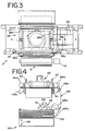
- FIG. 4 is a side view of a loading mechanism and the chemical-mechanical polishing apparatus for which the loading mechanism is used.
- FIG. 5 is a side view of a loading mechanism and the chemical-mechanecal polishing apparatus for which the loading mechanism is used.
- FIGS. 1, 2 , and 3 A preferred embodiment of an apparatus for chemically-mechanically polishing a semiconductor wafer is depicted in FIGS. 1, 2 , and 3 .
- the apparatus 2 is built about frame 4 and mounting plate 6 .
- An abrasive belt feed roll 10 holds a supply of wafer-polishing member 12 .
- a preferred wafer-polishing member comprises a flexible strip having an abrasive layer fixed onto the strip.
- the abrasive layer comprises a series of discrete cylindrical abrasive members such that as the abrasive layer becomes worn down through use, the surface area of the discrete cylindrical abrasive members remains substantially constant.
- the abrasive layer is preferably covered with a protective polymer layer. The polymer layer is removed before the abrasive can be used to polish a semiconductor wafer.
- This preferred wafer-polishing member is commercially available through the Minnesota Mining and Manufacturing Company as part numbers 3M 307EA and 3M 237AA, which are available in grades A100, A65, A45, A16, and A6.
- the wafer-polishing member comprises a polishing pad adapted to receive an abrasive slurry such as the slurries disclosed in U.S. Pat. Nos. 6,007,407, 6,012,966 and 6,022,266. These patents are incorporated by reference in their entirety.
- a suitable polishing pad material is commercially available from the Rodel Corporation of Delaware.
- belt tension control 14 Attached to a sidewall of abrasive belt feed roll 10 is belt tension control 14 .
- belt tension control 14 When belt tension control 14 is off, feed roll 10 is free to rotate. Any known belt tension control mechanism is contemplated for use with this embodiment.
- the preferred belt tension control 14 can be activated many ways, including but not limited to electronically, pneumatically, hydraulically or a combination.
- each of the above embodiments described herein may utilize a non-abrasive liquid during polishing, such as deionized water, to facilitate the polishing process.
- the non-abrasive liquid may be applied via nozzles 43 (See FIG. 1) to the region of the polishing strip intended for contact with a wafer.
- Belt conditioner 20 is positioned between belt feed roll 10 and ingress rollers 22 a and 22 b .
- belt conditioner 20 conditions the wafer-polishing member 12 before polishing member 12 is used to polish a semiconductor wafer.
- belt conditioner 20 removes the protective polymer layer from the wafer-polishing member 12 .
- Suitable belt conditioners 20 include, but are not limited to, the conditioners described in U.S. Pat. Nos. 6,022,266, 5,938,507, and 5,934,980, which are hereby incorporated by reference in their entirety.
- there is no belt conditioner 20 because the process of polishing occurs simultaneously with the process of conditioning. This is described in greater detail supra in this specification.
- Ingress roller 22 a is powered, and ingress roller 22 b is not powered. In alternative embodiments, both rollers can be powered or roller 22 b can be powered while 22 a is not.
- Wafer-polishing member 12 is in contact with belt conditioner 20 and ingress rollers 22 a and 22 b . In the depicted embodiment, wafer-polishing member 12 frictionally fits between ingress rollers 22 a and 22 b . These rollers move wafer-polishing member 12 onto a receiving surface 30 . That is, through ingress rollers 22 a and 22 b , a measured portion of wafer-polishing member 12 is pulled from feed roll 10 onto receiving surface 30 .
- clamps 26 a and 26 b secure the measured portion of wafer-polishing member 12 onto receiving surface 30 .
- Clamps are merely an exemplary securing mechanism. Any securing mechanism known in the art could be used to secure wafer-polishing member 12 onto receiving surface 30 .
- Receiving surface 30 has an ingress side and an egress side.
- belt cutter 27 is positioned above receiving surface 30 on the ingress side.
- belt cutter 27 is positioned above receiving surface 30 on the egress side.
- the position of the belt cutter 27 determines how much of the chemical mechanical polishing assembly oscillates with receiving surface 30 along guide rails 36 a and 36 b when polishing occurs.
- Reciprocating table 32 is attached to reciprocation drive assembly 35 .
- Preferred drive assemblies 35 include a crank shaft, drive motor, connecting rods, and a counter balance.
- a preferred drive assembly reciprocates linearly (+/ ⁇ one inch) at an adjustable frequency of from about 0 to about 25 Hertz.
- Reciprocating table 32 reciprocates in guide rails 36 a and 36 b . It is preferred that the guide rails have linear bearings.
- the moving parts include clamps 26 a and 26 b , egress roller 28 b , driven portions of reciprocation drive assembly 35 that impart reciprocation motion onto reciprocated table 32 and counterweight 34 .
- the following additional parts move with receiving surface 30 : feed roll 10 , belt tension control 14 , ingress rollers 22 a and 22 b , and egress roller 28 a.
- Egress rollers 28 a and 28 b are in contact with wafer-polishing member 12 on the egress side of receiving surface 30 .
- Egress roller 28 a is powered, and egress roller 28 b is not powered. In other embodiments, both rollers may be powered or roller 28 b may be powered while roller 28 a is not.
- Belt disposal container 29 is positioned to receive spent measured portions of wafer-polishing member 12 from egress rollers 28 a and 28 b . Any container or disposal mechanism known to those of skill in the art for disposing of spent measured portions of wafer-polishing member 12 is contemplated for use in this embodiment.
- receiving surface 30 comprises reciprocating table 32 positioned above air-bearing platen assembly 34 .
- Platen assemblies contemplated for use with this embodiment can be any known platen assembly, including but not limited to the platen assemblies disclosed in U.S. Pat. Nos. 5,558,568, 5,985,093, 6,000,997, 6,015,499 and 6,015,506, which are hereby incorporated by reference.
- Other acceptable platens are those commercially available from the Lam Research Corporation of Fremont, California, including the ones with the trade name TERES. Note that some of these platens are rotating platen assemblies.
- the platen assemblies contemplated for use with this embodiment are preferably not rotating.
- Wafer holder 40 comprises spindle 42 and carrier head 44 .
- Carrier head 44 releasably holds wafer 46 .
- wafer 46 is pressed against wafer-polishing member 12 by the wafer holder 40 .
- Spindle 42 rotates carrier head 44 and wafer 46 about an axis perpendicular to receiving surface 30 as wafer polishing member 12 reciprocates with reciprocating table 32 along guide rails 36 a and 36 b .
- wafer holder 40 does not rotate wafer 46 , but instead holds wafer 46 stationary while polishing member 12 reciprocates with reciprocating table 32 along guide rails 36 a and 36 b.
- the method works as follows.
- a supply of wafer polishing member 12 is kept on belt feed roll 10 .
- the belt conditioner 24 conditions the wafer-polishing member 12 as it is drawn off of the feed roll so that it is ready to polish wafer 46 .
- a measured portion of the wafer polishing member 12 is fed through ingress rollers 22 a and 22 b , then secured to receiving surface 30 with clamps 26 a and 26 b .
- This measured portion is preferably about 8 inches in length.
- belt cutter 27 cuts the measured portion of wafer polishing member 12 , separating the wafer polishing member from the remainder of the belt feed roll 10 .
- the reciprocation drive assembly reciprocates the receiving surface 30 , and all the parts attached therewith reciprocate along guide rails 36 a and 36 b.
- wafer holder 40 which is holding wafer 46 , is brought into contact with the measured portion of polishing member 12 .
- Wafer holder 40 spins about an axis perpendicular to receiving surface 30 while polishing member 12 reciprocates with the receiving surface.
- Wafer 46 is polished by the combination of spinning and reciprocating.
- the measured portion of polishing member 12 is taken through egress rollers 28 a and 28 b , and is discarded into disposal container 29 .
- belt conditioner 20 is omitted.
- the alternative apparatus works as follows. A supply of wafer polishing member 12 is kept on belt feed roll 10 . A measured portion of the wafer polishing member 12 is fed through ingress rollers 22 a and 22 b , then secured to receiving surface 30 with clamps 26 a and 26 b . This measured portion is small, preferably less than one inch in length, more preferably less than one-half inch, and most preferably about 1 ⁇ 4 inch. Then, the receiving surface 30 and all the parts attached therewith reciprocate along guide rails 36 a and 36 b .
- Wafer holder 40 which is holding wafer 46 , is in contact with the measured portion of polishing member 12 .
- Wafer holder 40 spins about an axis perpendicular to receiving surface 30 while polishing member 12 reciprocates with the receiving surface.
- Wafer 46 is polished at the same time the wafer is conditioned by the combination of spinning and reciprocating.
- the first small measured portion is complete, the next small measured portion is pulled onto receiving surface 30 and the reciprocation process is repeated. This occurs until the entire wafer 46 is polished and the polishing member 12 is conditioned.
- a measured portion of polishing member 12 has been conditioned, small or otherwise, it is preferably used to polish more than one wafer 46 .
- the belt cutter 27 cuts off the spent portion of polishing member 12 . Then, the measured portion of polishing member 12 is taken through egress rollers 28 a and 28 b , and is discarded into disposal container 29 . Any mechanism for disposing of spent polishing member is within the scope of the described embodiment. Such mechanisms include but are not limited to take-up rollers.
- an apparatus for chemically-mechanically polishing semiconductor wafers has an improved loading mechanism for loading discrete sheets of polishing member 12 onto a receiving surface 30 .
- FIGS. 4 and 5 two embodiments of a loading mechanism are shown.
- loading mechanism 100 is shown.
- Supply bin 105 contains a supply of discrete sheets of polishing member 12 .
- Feed roll 110 makes a first discrete sheet available to a web pick up vacuum member 115 .
- there is only one web pick up vacuum member 115 In the embodiment depicted in FIG. 5, there are two web pick up vacuum members 115 .
- Vacuum member 115 is attached to a frame at a pivot point 120 . Vacuum member 115 makes contact with a discreet sheet of polishing member 12 , rotates about the pivot point 120 , and delivers the discreet sheet of polishing member 12 to transfer rollers 125 a and 125 b . Then, in FIG. 4, the discreet sheet of polishing member 12 is slid along web transfer guide 126 where it is fed to ingress rollers 128 a and 128 b . In FIG. 5, no transfer guide 126 is shown, but such a guide is optional and can be included in the assembly.
- the supply bin's position is adjusted using any indexing mechanism known to those of skill in the art.
- Exemplary non-limiting indexing mechanisms are disclosed in U.S. Pat. Nos. 4,248,413, 4,807,868, and 5,013,026. These patents are hereby incorporated by reference.
- the discreet sheets of polishing member 12 be durable enough to remain undamaged while being stacked in a pile and being handled by several sets of rollers and a vacuum member 115 .
- the abrasive be a fixed abrasive as described above.
Landscapes
- Engineering & Computer Science (AREA)
- Mechanical Engineering (AREA)
- Mechanical Treatment Of Semiconductor (AREA)
- Finish Polishing, Edge Sharpening, And Grinding By Specific Grinding Devices (AREA)
Abstract
Description
Claims (27)
Priority Applications (1)
| Application Number | Priority Date | Filing Date | Title |
|---|---|---|---|
| US09/540,385 US6261959B1 (en) | 2000-03-31 | 2000-03-31 | Method and apparatus for chemically-mechanically polishing semiconductor wafers |
Applications Claiming Priority (1)
| Application Number | Priority Date | Filing Date | Title |
|---|---|---|---|
| US09/540,385 US6261959B1 (en) | 2000-03-31 | 2000-03-31 | Method and apparatus for chemically-mechanically polishing semiconductor wafers |
Publications (1)
| Publication Number | Publication Date |
|---|---|
| US6261959B1 true US6261959B1 (en) | 2001-07-17 |
Family
ID=24155227
Family Applications (1)
| Application Number | Title | Priority Date | Filing Date |
|---|---|---|---|
| US09/540,385 Expired - Fee Related US6261959B1 (en) | 2000-03-31 | 2000-03-31 | Method and apparatus for chemically-mechanically polishing semiconductor wafers |
Country Status (1)
| Country | Link |
|---|---|
| US (1) | US6261959B1 (en) |
Cited By (38)
| Publication number | Priority date | Publication date | Assignee | Title |
|---|---|---|---|---|
| US6435952B1 (en) | 2000-06-30 | 2002-08-20 | Lam Research Corporation | Apparatus and method for qualifying a chemical mechanical planarization process |
| US20020123298A1 (en) * | 2000-06-30 | 2002-09-05 | Lam Research Corporation | Linear reciprocating disposable belt polishing method and apparatus |
| US20020173225A1 (en) * | 1998-12-01 | 2002-11-21 | Yuchun Wang | Chemical mechanical polishing endpoint detection |
| US20030072639A1 (en) * | 2001-10-17 | 2003-04-17 | Applied Materials, Inc. | Substrate support |
| US20030213703A1 (en) * | 2002-05-16 | 2003-11-20 | Applied Materials, Inc. | Method and apparatus for substrate polishing |
| US20030220053A1 (en) * | 2000-02-17 | 2003-11-27 | Applied Materials, Inc. | Apparatus for electrochemical processing |
| US20040023607A1 (en) * | 2002-03-13 | 2004-02-05 | Homayoun Talieh | Method and apparatus for integrated chemical mechanical polishing of copper and barrier layers |
| US6722946B2 (en) | 2002-01-17 | 2004-04-20 | Nutool, Inc. | Advanced chemical mechanical polishing system with smart endpoint detection |
| US6808442B1 (en) * | 2001-12-20 | 2004-10-26 | Lam Research Corporation | Apparatus for removal/remaining thickness profile manipulation |
| US6857947B2 (en) | 2002-01-17 | 2005-02-22 | Asm Nutool, Inc | Advanced chemical mechanical polishing system with smart endpoint detection |
| US20050124262A1 (en) * | 2003-12-03 | 2005-06-09 | Applied Materials, Inc. | Processing pad assembly with zone control |
| US20050173259A1 (en) * | 2004-02-06 | 2005-08-11 | Applied Materials, Inc. | Endpoint system for electro-chemical mechanical polishing |
| US6942546B2 (en) | 2002-01-17 | 2005-09-13 | Asm Nutool, Inc. | Endpoint detection for non-transparent polishing member |
| US20050221723A1 (en) * | 2003-10-03 | 2005-10-06 | Applied Materials, Inc. | Multi-layer polishing pad for low-pressure polishing |
| US6962524B2 (en) | 2000-02-17 | 2005-11-08 | Applied Materials, Inc. | Conductive polishing article for electrochemical mechanical polishing |
| US6979248B2 (en) | 2002-05-07 | 2005-12-27 | Applied Materials, Inc. | Conductive polishing article for electrochemical mechanical polishing |
| US6988942B2 (en) | 2000-02-17 | 2006-01-24 | Applied Materials Inc. | Conductive polishing article for electrochemical mechanical polishing |
| US6991528B2 (en) | 2000-02-17 | 2006-01-31 | Applied Materials, Inc. | Conductive polishing article for electrochemical mechanical polishing |
| US7014538B2 (en) | 1999-05-03 | 2006-03-21 | Applied Materials, Inc. | Article for polishing semiconductor substrates |
| US7029365B2 (en) | 2000-02-17 | 2006-04-18 | Applied Materials Inc. | Pad assembly for electrochemical mechanical processing |
| US7059948B2 (en) | 2000-12-22 | 2006-06-13 | Applied Materials | Articles for polishing semiconductor substrates |
| US7077721B2 (en) | 2000-02-17 | 2006-07-18 | Applied Materials, Inc. | Pad assembly for electrochemical mechanical processing |
| US7084064B2 (en) | 2004-09-14 | 2006-08-01 | Applied Materials, Inc. | Full sequence metal and barrier layer electrochemical mechanical processing |
| US7125477B2 (en) | 2000-02-17 | 2006-10-24 | Applied Materials, Inc. | Contacts for electrochemical processing |
| US7137879B2 (en) | 2001-04-24 | 2006-11-21 | Applied Materials, Inc. | Conductive polishing article for electrochemical mechanical polishing |
| US7294038B2 (en) | 2002-09-16 | 2007-11-13 | Applied Materials, Inc. | Process control in electrochemically assisted planarization |
| US7303462B2 (en) | 2000-02-17 | 2007-12-04 | Applied Materials, Inc. | Edge bead removal by an electro polishing process |
| US7303662B2 (en) | 2000-02-17 | 2007-12-04 | Applied Materials, Inc. | Contacts for electrochemical processing |
| US7323095B2 (en) | 2000-12-18 | 2008-01-29 | Applied Materials, Inc. | Integrated multi-step gap fill and all feature planarization for conductive materials |
| US7344432B2 (en) | 2001-04-24 | 2008-03-18 | Applied Materials, Inc. | Conductive pad with ion exchange membrane for electrochemical mechanical polishing |
| US7374644B2 (en) | 2000-02-17 | 2008-05-20 | Applied Materials, Inc. | Conductive polishing article for electrochemical mechanical polishing |
| US7427340B2 (en) | 2005-04-08 | 2008-09-23 | Applied Materials, Inc. | Conductive pad |
| US7520968B2 (en) | 2004-10-05 | 2009-04-21 | Applied Materials, Inc. | Conductive pad design modification for better wafer-pad contact |
| US7670468B2 (en) | 2000-02-17 | 2010-03-02 | Applied Materials, Inc. | Contact assembly and method for electrochemical mechanical processing |
| US7678245B2 (en) | 2000-02-17 | 2010-03-16 | Applied Materials, Inc. | Method and apparatus for electrochemical mechanical processing |
| US10786885B2 (en) | 2017-01-20 | 2020-09-29 | Applied Materials, Inc. | Thin plastic polishing article for CMP applications |
| US20230158634A1 (en) * | 2021-11-25 | 2023-05-25 | Industrial Technology Research Institute | Polish pad replacing apparatus |
| US11717936B2 (en) | 2018-09-14 | 2023-08-08 | Applied Materials, Inc. | Methods for a web-based CMP system |
Citations (25)
| Publication number | Priority date | Publication date | Assignee | Title |
|---|---|---|---|---|
| US3753269A (en) | 1971-05-21 | 1973-08-21 | R Budman | Abrasive cloth cleaner |
| US4318250A (en) | 1980-03-31 | 1982-03-09 | St. Florian Company, Ltd. | Wafer grinder |
| US4720939A (en) | 1986-05-23 | 1988-01-26 | Simpson Products, Inc. | Wide belt sander cleaning device |
| US4934102A (en) | 1988-10-04 | 1990-06-19 | International Business Machines Corporation | System for mechanical planarization |
| US5081051A (en) | 1990-09-12 | 1992-01-14 | Intel Corporation | Method for conditioning the surface of a polishing pad |
| US5335453A (en) | 1991-06-06 | 1994-08-09 | Commissariat A L'energie Atomique | Polishing machine having a taut microabrasive strip and an improved wafer support head |
| US5484323A (en) | 1991-07-22 | 1996-01-16 | Smith; Robert K. | Belt cleaner |
| US5536202A (en) | 1994-07-27 | 1996-07-16 | Texas Instruments Incorporated | Semiconductor substrate conditioning head having a plurality of geometries formed in a surface thereof for pad conditioning during chemical-mechanical polish |
| US5547417A (en) | 1994-03-21 | 1996-08-20 | Intel Corporation | Method and apparatus for conditioning a semiconductor polishing pad |
| US5558568A (en) | 1994-10-11 | 1996-09-24 | Ontrak Systems, Inc. | Wafer polishing machine with fluid bearings |
| US5575707A (en) | 1994-10-11 | 1996-11-19 | Ontrak Systems, Inc. | Polishing pad cluster for polishing a semiconductor wafer |
| US5611943A (en) | 1995-09-29 | 1997-03-18 | Intel Corporation | Method and apparatus for conditioning of chemical-mechanical polishing pads |
| US5622526A (en) | 1994-03-28 | 1997-04-22 | J. D. Phillips Corporation | Apparatus for trueing CBN abrasive belts and grinding wheels |
| US5643044A (en) | 1994-11-01 | 1997-07-01 | Lund; Douglas E. | Automatic chemical and mechanical polishing system for semiconductor wafers |
| US5655951A (en) | 1995-09-29 | 1997-08-12 | Micron Technology, Inc. | Method for selectively reconditioning a polishing pad used in chemical-mechanical planarization of semiconductor wafers |
| US5692947A (en) | 1994-08-09 | 1997-12-02 | Ontrak Systems, Inc. | Linear polisher and method for semiconductor wafer planarization |
| US5692950A (en) | 1996-08-08 | 1997-12-02 | Minnesota Mining And Manufacturing Company | Abrasive construction for semiconductor wafer modification |
| US5759918A (en) | 1995-05-18 | 1998-06-02 | Obsidian, Inc. | Method for chemical mechanical polishing |
| US5762536A (en) | 1996-04-26 | 1998-06-09 | Lam Research Corporation | Sensors for a linear polisher |
| WO1998045090A1 (en) | 1997-04-04 | 1998-10-15 | Obsidian, Inc. | Polishing media magazine for improved polishing |
| US5871390A (en) | 1997-02-06 | 1999-02-16 | Lam Research Corporation | Method and apparatus for aligning and tensioning a pad/belt used in linear planarization for chemical mechanical polishing |
| US5897426A (en) | 1998-04-24 | 1999-04-27 | Applied Materials, Inc. | Chemical mechanical polishing with multiple polishing pads |
| US5899798A (en) | 1997-07-25 | 1999-05-04 | Obsidian Inc. | Low profile, low hysteresis force feedback gimbal system for chemical mechanical polishing |
| WO1999022908A1 (en) | 1997-10-31 | 1999-05-14 | Obsidian, Inc. | Linear drive system for chemical mechanical polishing |
| US5958794A (en) | 1995-09-22 | 1999-09-28 | Minnesota Mining And Manufacturing Company | Method of modifying an exposed surface of a semiconductor wafer |
-
2000
- 2000-03-31 US US09/540,385 patent/US6261959B1/en not_active Expired - Fee Related
Patent Citations (27)
| Publication number | Priority date | Publication date | Assignee | Title |
|---|---|---|---|---|
| US3753269A (en) | 1971-05-21 | 1973-08-21 | R Budman | Abrasive cloth cleaner |
| US4318250A (en) | 1980-03-31 | 1982-03-09 | St. Florian Company, Ltd. | Wafer grinder |
| US4720939A (en) | 1986-05-23 | 1988-01-26 | Simpson Products, Inc. | Wide belt sander cleaning device |
| US4934102A (en) | 1988-10-04 | 1990-06-19 | International Business Machines Corporation | System for mechanical planarization |
| US5081051A (en) | 1990-09-12 | 1992-01-14 | Intel Corporation | Method for conditioning the surface of a polishing pad |
| US5335453A (en) | 1991-06-06 | 1994-08-09 | Commissariat A L'energie Atomique | Polishing machine having a taut microabrasive strip and an improved wafer support head |
| US5484323A (en) | 1991-07-22 | 1996-01-16 | Smith; Robert K. | Belt cleaner |
| US5547417A (en) | 1994-03-21 | 1996-08-20 | Intel Corporation | Method and apparatus for conditioning a semiconductor polishing pad |
| US5622526A (en) | 1994-03-28 | 1997-04-22 | J. D. Phillips Corporation | Apparatus for trueing CBN abrasive belts and grinding wheels |
| US5536202A (en) | 1994-07-27 | 1996-07-16 | Texas Instruments Incorporated | Semiconductor substrate conditioning head having a plurality of geometries formed in a surface thereof for pad conditioning during chemical-mechanical polish |
| US5692947A (en) | 1994-08-09 | 1997-12-02 | Ontrak Systems, Inc. | Linear polisher and method for semiconductor wafer planarization |
| US5558568A (en) | 1994-10-11 | 1996-09-24 | Ontrak Systems, Inc. | Wafer polishing machine with fluid bearings |
| US5575707A (en) | 1994-10-11 | 1996-11-19 | Ontrak Systems, Inc. | Polishing pad cluster for polishing a semiconductor wafer |
| US5593344A (en) | 1994-10-11 | 1997-01-14 | Ontrak Systems, Inc. | Wafer polishing machine with fluid bearings and drive systems |
| US5643044A (en) | 1994-11-01 | 1997-07-01 | Lund; Douglas E. | Automatic chemical and mechanical polishing system for semiconductor wafers |
| US5759918A (en) | 1995-05-18 | 1998-06-02 | Obsidian, Inc. | Method for chemical mechanical polishing |
| US5908530A (en) | 1995-05-18 | 1999-06-01 | Obsidian, Inc. | Apparatus for chemical mechanical polishing |
| US5958794A (en) | 1995-09-22 | 1999-09-28 | Minnesota Mining And Manufacturing Company | Method of modifying an exposed surface of a semiconductor wafer |
| US5655951A (en) | 1995-09-29 | 1997-08-12 | Micron Technology, Inc. | Method for selectively reconditioning a polishing pad used in chemical-mechanical planarization of semiconductor wafers |
| US5611943A (en) | 1995-09-29 | 1997-03-18 | Intel Corporation | Method and apparatus for conditioning of chemical-mechanical polishing pads |
| US5762536A (en) | 1996-04-26 | 1998-06-09 | Lam Research Corporation | Sensors for a linear polisher |
| US5692950A (en) | 1996-08-08 | 1997-12-02 | Minnesota Mining And Manufacturing Company | Abrasive construction for semiconductor wafer modification |
| US5871390A (en) | 1997-02-06 | 1999-02-16 | Lam Research Corporation | Method and apparatus for aligning and tensioning a pad/belt used in linear planarization for chemical mechanical polishing |
| WO1998045090A1 (en) | 1997-04-04 | 1998-10-15 | Obsidian, Inc. | Polishing media magazine for improved polishing |
| US5899798A (en) | 1997-07-25 | 1999-05-04 | Obsidian Inc. | Low profile, low hysteresis force feedback gimbal system for chemical mechanical polishing |
| WO1999022908A1 (en) | 1997-10-31 | 1999-05-14 | Obsidian, Inc. | Linear drive system for chemical mechanical polishing |
| US5897426A (en) | 1998-04-24 | 1999-04-27 | Applied Materials, Inc. | Chemical mechanical polishing with multiple polishing pads |
Cited By (58)
| Publication number | Priority date | Publication date | Assignee | Title |
|---|---|---|---|---|
| US6908374B2 (en) * | 1998-12-01 | 2005-06-21 | Nutool, Inc. | Chemical mechanical polishing endpoint detection |
| US20020173225A1 (en) * | 1998-12-01 | 2002-11-21 | Yuchun Wang | Chemical mechanical polishing endpoint detection |
| US7014538B2 (en) | 1999-05-03 | 2006-03-21 | Applied Materials, Inc. | Article for polishing semiconductor substrates |
| US7077721B2 (en) | 2000-02-17 | 2006-07-18 | Applied Materials, Inc. | Pad assembly for electrochemical mechanical processing |
| US7029365B2 (en) | 2000-02-17 | 2006-04-18 | Applied Materials Inc. | Pad assembly for electrochemical mechanical processing |
| US7678245B2 (en) | 2000-02-17 | 2010-03-16 | Applied Materials, Inc. | Method and apparatus for electrochemical mechanical processing |
| US20030220053A1 (en) * | 2000-02-17 | 2003-11-27 | Applied Materials, Inc. | Apparatus for electrochemical processing |
| US7278911B2 (en) | 2000-02-17 | 2007-10-09 | Applied Materials, Inc. | Conductive polishing article for electrochemical mechanical polishing |
| US7670468B2 (en) | 2000-02-17 | 2010-03-02 | Applied Materials, Inc. | Contact assembly and method for electrochemical mechanical processing |
| US7569134B2 (en) | 2000-02-17 | 2009-08-04 | Applied Materials, Inc. | Contacts for electrochemical processing |
| US7125477B2 (en) | 2000-02-17 | 2006-10-24 | Applied Materials, Inc. | Contacts for electrochemical processing |
| US7422516B2 (en) | 2000-02-17 | 2008-09-09 | Applied Materials, Inc. | Conductive polishing article for electrochemical mechanical polishing |
| US7374644B2 (en) | 2000-02-17 | 2008-05-20 | Applied Materials, Inc. | Conductive polishing article for electrochemical mechanical polishing |
| US6884153B2 (en) | 2000-02-17 | 2005-04-26 | Applied Materials, Inc. | Apparatus for electrochemical processing |
| US7344431B2 (en) | 2000-02-17 | 2008-03-18 | Applied Materials, Inc. | Pad assembly for electrochemical mechanical processing |
| US7137868B2 (en) | 2000-02-17 | 2006-11-21 | Applied Materials, Inc. | Pad assembly for electrochemical mechanical processing |
| US7285036B2 (en) | 2000-02-17 | 2007-10-23 | Applied Materials, Inc. | Pad assembly for electrochemical mechanical polishing |
| US20080026681A1 (en) * | 2000-02-17 | 2008-01-31 | Butterfield Paul D | Conductive polishing article for electrochemical mechanical polishing |
| US7303462B2 (en) | 2000-02-17 | 2007-12-04 | Applied Materials, Inc. | Edge bead removal by an electro polishing process |
| US6962524B2 (en) | 2000-02-17 | 2005-11-08 | Applied Materials, Inc. | Conductive polishing article for electrochemical mechanical polishing |
| US20060148381A1 (en) * | 2000-02-17 | 2006-07-06 | Applied Materials, Inc. | Pad assembly for electrochemical mechanical processing |
| US6988942B2 (en) | 2000-02-17 | 2006-01-24 | Applied Materials Inc. | Conductive polishing article for electrochemical mechanical polishing |
| US6991528B2 (en) | 2000-02-17 | 2006-01-31 | Applied Materials, Inc. | Conductive polishing article for electrochemical mechanical polishing |
| US7207878B2 (en) | 2000-02-17 | 2007-04-24 | Applied Materials, Inc. | Conductive polishing article for electrochemical mechanical polishing |
| US7303662B2 (en) | 2000-02-17 | 2007-12-04 | Applied Materials, Inc. | Contacts for electrochemical processing |
| US20020123298A1 (en) * | 2000-06-30 | 2002-09-05 | Lam Research Corporation | Linear reciprocating disposable belt polishing method and apparatus |
| US6435952B1 (en) | 2000-06-30 | 2002-08-20 | Lam Research Corporation | Apparatus and method for qualifying a chemical mechanical planarization process |
| US6746320B2 (en) * | 2000-06-30 | 2004-06-08 | Lam Research Corporation | Linear reciprocating disposable belt polishing method and apparatus |
| US6500056B1 (en) | 2000-06-30 | 2002-12-31 | Lam Research Corporation | Linear reciprocating disposable belt polishing method and apparatus |
| US6679763B2 (en) | 2000-06-30 | 2004-01-20 | Lam Research Corporation | Apparatus and method for qualifying a chemical mechanical planarization process |
| US7323095B2 (en) | 2000-12-18 | 2008-01-29 | Applied Materials, Inc. | Integrated multi-step gap fill and all feature planarization for conductive materials |
| US7059948B2 (en) | 2000-12-22 | 2006-06-13 | Applied Materials | Articles for polishing semiconductor substrates |
| US7311592B2 (en) | 2001-04-24 | 2007-12-25 | Applied Materials, Inc. | Conductive polishing article for electrochemical mechanical polishing |
| US7344432B2 (en) | 2001-04-24 | 2008-03-18 | Applied Materials, Inc. | Conductive pad with ion exchange membrane for electrochemical mechanical polishing |
| US7137879B2 (en) | 2001-04-24 | 2006-11-21 | Applied Materials, Inc. | Conductive polishing article for electrochemical mechanical polishing |
| US20030072639A1 (en) * | 2001-10-17 | 2003-04-17 | Applied Materials, Inc. | Substrate support |
| US6808442B1 (en) * | 2001-12-20 | 2004-10-26 | Lam Research Corporation | Apparatus for removal/remaining thickness profile manipulation |
| US6722946B2 (en) | 2002-01-17 | 2004-04-20 | Nutool, Inc. | Advanced chemical mechanical polishing system with smart endpoint detection |
| US6857947B2 (en) | 2002-01-17 | 2005-02-22 | Asm Nutool, Inc | Advanced chemical mechanical polishing system with smart endpoint detection |
| US7097538B2 (en) | 2002-01-17 | 2006-08-29 | Asm Nutool, Inc. | Advanced chemical mechanical polishing system with smart endpoint detection |
| US20060063469A1 (en) * | 2002-01-17 | 2006-03-23 | Homayoun Talieh | Advanced chemical mechanical polishing system with smart endpoint detection |
| US6942546B2 (en) | 2002-01-17 | 2005-09-13 | Asm Nutool, Inc. | Endpoint detection for non-transparent polishing member |
| US20040023607A1 (en) * | 2002-03-13 | 2004-02-05 | Homayoun Talieh | Method and apparatus for integrated chemical mechanical polishing of copper and barrier layers |
| US6979248B2 (en) | 2002-05-07 | 2005-12-27 | Applied Materials, Inc. | Conductive polishing article for electrochemical mechanical polishing |
| US20030213703A1 (en) * | 2002-05-16 | 2003-11-20 | Applied Materials, Inc. | Method and apparatus for substrate polishing |
| US7294038B2 (en) | 2002-09-16 | 2007-11-13 | Applied Materials, Inc. | Process control in electrochemically assisted planarization |
| US20050221723A1 (en) * | 2003-10-03 | 2005-10-06 | Applied Materials, Inc. | Multi-layer polishing pad for low-pressure polishing |
| US8066552B2 (en) | 2003-10-03 | 2011-11-29 | Applied Materials, Inc. | Multi-layer polishing pad for low-pressure polishing |
| US7186164B2 (en) | 2003-12-03 | 2007-03-06 | Applied Materials, Inc. | Processing pad assembly with zone control |
| US20050124262A1 (en) * | 2003-12-03 | 2005-06-09 | Applied Materials, Inc. | Processing pad assembly with zone control |
| US20050173259A1 (en) * | 2004-02-06 | 2005-08-11 | Applied Materials, Inc. | Endpoint system for electro-chemical mechanical polishing |
| US7446041B2 (en) | 2004-09-14 | 2008-11-04 | Applied Materials, Inc. | Full sequence metal and barrier layer electrochemical mechanical processing |
| US7084064B2 (en) | 2004-09-14 | 2006-08-01 | Applied Materials, Inc. | Full sequence metal and barrier layer electrochemical mechanical processing |
| US7520968B2 (en) | 2004-10-05 | 2009-04-21 | Applied Materials, Inc. | Conductive pad design modification for better wafer-pad contact |
| US7427340B2 (en) | 2005-04-08 | 2008-09-23 | Applied Materials, Inc. | Conductive pad |
| US10786885B2 (en) | 2017-01-20 | 2020-09-29 | Applied Materials, Inc. | Thin plastic polishing article for CMP applications |
| US11717936B2 (en) | 2018-09-14 | 2023-08-08 | Applied Materials, Inc. | Methods for a web-based CMP system |
| US20230158634A1 (en) * | 2021-11-25 | 2023-05-25 | Industrial Technology Research Institute | Polish pad replacing apparatus |
Similar Documents
| Publication | Publication Date | Title |
|---|---|---|
| US6261959B1 (en) | Method and apparatus for chemically-mechanically polishing semiconductor wafers | |
| US6428394B1 (en) | Method and apparatus for chemical mechanical planarization and polishing of semiconductor wafers using a continuous polishing member feed | |
| US6179690B1 (en) | Substrate polishing apparatus | |
| US7993485B2 (en) | Methods and apparatus for processing a substrate | |
| TWI278926B (en) | Apparatus and method of polishing periphery of device wafer | |
| US6793558B2 (en) | Method and apparatus for planarizing a microelectronic substrate with a tilted planarizing surface | |
| US6306016B1 (en) | Wafer notch polishing machine and method of polishing an orientation notch in a wafer | |
| DE60102891T2 (en) | DEVICE AND METHOD FOR CONTROLLED POLISHING AND PLANARIZATION OF SEMICONDUCTOR GRINDING | |
| JPH0741591B2 (en) | Cutter head for cutting sheet material | |
| US20090017731A1 (en) | Methods and apparatus for processing a substrate | |
| EP1738870A1 (en) | Polisher | |
| EP1813384A1 (en) | Grinding device and grinding system | |
| KR20170032928A (en) | Apparatus for Grinding Side Edge of Thin Glass Cover | |
| JPH081494A (en) | Wafer material edge end part polishing device | |
| KR101236855B1 (en) | Methods and apparatus for processing a substrate | |
| CN210413974U (en) | Feeding-amount-adjustable abrasive belt winding and unwinding device | |
| JP2534602B2 (en) | Belt sander for metal processing | |
| JP3404579B2 (en) | Polishing device for both shafts | |
| JP2006181697A (en) | Surface polishing device and method | |
| US5807167A (en) | Foam pad resurfacer | |
| JP2635252B2 (en) | Wide belt sander and method for producing forming roll | |
| JP2012218132A (en) | Deburring device | |
| JP2869624B2 (en) | Double-headed surface grinding machine for thin workpieces | |
| JP2869627B2 (en) | Super finishing device using abrasive film | |
| JP2599060B2 (en) | Belt sander for metal processing |
Legal Events
| Date | Code | Title | Description |
|---|---|---|---|
| AS | Assignment |
Owner name: LAM RESEARCH CORPORATION, CALIFORNIA Free format text: ASSIGNMENT OF ASSIGNORS INTEREST;ASSIGNORS:TRAVIS, GLENN;PENA, CHRISTOPHER;REEL/FRAME:011258/0340 Effective date: 20001030 |
|
| CC | Certificate of correction | ||
| FPAY | Fee payment |
Year of fee payment: 4 |
|
| AS | Assignment |
Owner name: APPLIED MATERIALS, INC., CALIFORNIA Free format text: ASSIGNMENT OF ASSIGNORS INTEREST;ASSIGNOR:LAM RESEARCH CORPORATION;REEL/FRAME:020951/0935 Effective date: 20080108 |
|
| REMI | Maintenance fee reminder mailed | ||
| LAPS | Lapse for failure to pay maintenance fees | ||
| STCH | Information on status: patent discontinuation |
Free format text: PATENT EXPIRED DUE TO NONPAYMENT OF MAINTENANCE FEES UNDER 37 CFR 1.362 |
|
| FP | Lapsed due to failure to pay maintenance fee |
Effective date: 20090717 |