US6111812A - Method and apparatus for adjusting control signal timing in a memory device - Google Patents
Method and apparatus for adjusting control signal timing in a memory device Download PDFInfo
- Publication number
- US6111812A US6111812A US09/361,025 US36102599A US6111812A US 6111812 A US6111812 A US 6111812A US 36102599 A US36102599 A US 36102599A US 6111812 A US6111812 A US 6111812A
- Authority
- US
- United States
- Prior art keywords
- signal
- time
- delay
- clock
- clock signal
- Prior art date
- Legal status (The legal status is an assumption and is not a legal conclusion. Google has not performed a legal analysis and makes no representation as to the accuracy of the status listed.)
- Expired - Lifetime
Links
Images


Classifications
-
- G—PHYSICS
- G11—INFORMATION STORAGE
- G11C—STATIC STORES
- G11C8/00—Arrangements for selecting an address in a digital store
- G11C8/18—Address timing or clocking circuits; Address control signal generation or management, e.g. for row address strobe [RAS] or column address strobe [CAS] signals
-
- G—PHYSICS
- G11—INFORMATION STORAGE
- G11C—STATIC STORES
- G11C7/00—Arrangements for writing information into, or reading information out from, a digital store
- G11C7/22—Read-write [R-W] timing or clocking circuits; Read-write [R-W] control signal generators or management
Definitions
- the present invention relates generally to control signal timing in semiconductor memory devices, and more particularly to a method and apparatus for selectively adjusting control signal timing in such memory devices.
- Semiconductor memory devices are used in a wide variety of applications. Such memory devices receive data for storage, in what is called a Write operation, and provide stored data to devices external to the memory, in what is called a Read operations.
- the memory device is accessed through a bus or multiple bus system by an external device or bus-master, such as a microprocessor, memory controller, or application specific integrated circuit (ASIC).
- the bus transfers address, data, and control signals between the memory device and the bus-master accessing the memory device.
- SRAMs static random access memories
- the SRAM may provide the data earlier than a time at which the bus-master is ready to retrieve such data.
- Bus contention may then result, in which data read from the SRAM is driven onto the bus while other data still resides on the bus. Consequently, two or more devices are sourcing/sinking relatively high currents for some conflicting period of time, thereby increasing risk of latchup effects, increasing system power consumption, increasing power and ground noise, and potentially resulting in erroneous data values.
- a method and apparatus for selectively adjusting control signal timing in an integrated circuit, such as a memory device, that receives a clock signal and performs internal operations including producing a control signal.
- Clock sensing circuitry receives the clock signal and responsively produces a speed signal having a value corresponding to the frequency of the clock signal.
- Control signal delay circuitry receives the control signal and the speed signal, and responsively produces a delayed control signal, with the time-delay relative to the control signal corresponding to the speed signal value.
- the control signal may be any of a wide variety of control signals produced internal to a memory device and controlling the internal operations thereof.
- the control signal may be a data output control signal controlling the timing of operations of data output circuitry included within the memory device.
- the control signal may be an address select control signal controlling the timing of access to an addressed location within the memory device.
- the clock sensing circuitry may include a plurality of series-connected time-delay circuits, each able to receive a signal at its input and produce a corresponding time-delayed signal at its output.
- the clock signal is received at the input of a first of the time-delay circuits.
- the clock sensing circuitry may further include a plurality of latching circuits, each coupled with respective one of the time-delay circuits and latching the value of the respective time-delayed signal. The speed signal value may then correspond with the combination of latched values.
- the control signal delay circuitry may include a plurality of time-delay circuits, each able to receive a signal at its input and produce a corresponding time-delay signal at its output with the control signal propagating through a selected number of these circuits.
- the control signal delay circuitry may further include delay select circuitry that receives the speed signal and correspondingly routes the memory control signal through a selected number of the time-delay circuits, with the selected number corresponding to the value of the speed signal.
- an SRAM device may be included within systems having operating speeds that would otherwise be too slow for the high speed access time of the SRAM device.
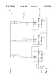
- FIG. 1 is a part functional block, part logic circuit diagram depicting a clock sensing circuit in accordance with an embodiment of the present invention.
- FIG. 2 is a logic circuit diagram depicting a delay latch circuit included in the clock sensing circuit of FIG. 1.
- FIG. 3 is a functional block circuit diagram depicting a memory device having an adjustable control signal delay circuit in accordance with an embodiment of the present invention.
- FIG. 4 is a part functional block, part logic circuit diagram depicting the control signal delay circuit of FIG. 3.
- FIG. 5 is a part functional block, part logic circuit diagram depicting a delay stage circuit included in the control signal delay circuit of FIG. 4.
- FIG. 6 is a functional block diagram depicting a computer system having a memory device in accordance with an embodiment of the present invention.
- FIG. 1 depicts a clock sensing circuit 10 in accordance with an embodiment of the present invention.
- the clock sensing circuit 10 receives a clock signal SYSCLK, senses the frequency of the clock signal, and produces a clock speed signal SLOW ⁇ 0:1> having a value corresponding to the frequency of the clock signal.
- the clock signal SYSCLK may be a system clock signal, such as that used to control data transfer operations between a memory device and a processor, system controller, or other bus-master.
- the clock sensing circuit 10 receives the clock signal SYSCLK at a toggle or divide-by-two circuit 12 that responsively produces a clock signal CLK having one-half the frequency of SYSCLK.
- the clock signal CLK is then routed through a plurality of series-connected time-delay circuits 14, which may be any of a wide variety of well-known circuits for delaying signal transmission.
- the time-delay circuits 14 may be of identical construction and may provide substantially the same time delay. Alternatively, the time-delay circuits 14 may vary, both in the particular circuit implementation and in the signal time-delay produced, as desired.
- One or more of the time-delay circuits 14 may include Reset inputs (not shown) to reset output signal states in response to, for example, a rising edge of the clock signal CLK.
- the clock sensing circuit 10 also includes a plurality of delay latch circuits 16, each coupled with a respective one of the time-delay circuits 14. Each of the delay latch circuits 16 receives the delayed clock signal output by the respective one of the time-delay circuits 14 and passes this signal to the input of a next one of the time-delay circuits. Each of the delay latch circuits 16 also receives the undelayed clock signal CLK and its complement CLK, which serve as latching control signals to latch the value of the delayed clock signal output by the respective one of the time-delay circuits 14. The latched value of the delayed clock signal is provided at a latched output of the delay latch circuit 16 as part of a four line delay signal DELAY ⁇ 0:3>.
- the delay latch circuits 16 may also include direct Latch, Reset, and/or Disable inputs and associated internal circuitry (not shown) to directly latch signal values, reset signal values, and/or disable the delay latch circuits independent of the state of the clock signal CLK.
- the delayed clock signal propagates through the series of timedelay circuits 14 and respective delay latch circuits 16, with the time delay being progressively greater as determined by the number of time-delay circuits through which the signal propagates.
- the undelayed clock signal CLK and its complement CLK latch the state of the delayed clock signal in each of the delay latch circuits 16, thereby indicating how far the delayed clock signal has propagated through the series of time-delay circuits 14.
- the delay signal DELAY ⁇ 0:3> then has four possible values (1000, 1100, 1110, or 1111), depending on how far the delayed clock signal has propagated through the time-delay circuits 14.
- the delay signal DELAY ⁇ 0:3> is converted into a two bit clock speed signal SLOW ⁇ 0:1> in a conventional fashion, such as by employing the particular conversion logic circuitry 18 shown in FIG. 1.
- each of the delay latch circuits 16 has its delay signal output set to a logic low state (or zero) in response to a rising edge of the clock signal CLK.
- the clock signal propagates through the series of time-delay circuits 14 and delay latch circuits 16, with each of the delay latch circuits then latching the output signal of the respective time-delay circuit 14 in response to a falling edge of the clock signal CLK.
- Each of the component signals of the delay signal DELAY ⁇ 0:3> is high or low depending on whether the delayed high state of the clock signal CLK has reached the corresponding delay latch circuit 16 when the falling edge of the clock signal CLK is applied to the delay latch.
- the clock signal CLK is one-half the frequency of the clock signal SYSCLK
- the signal latched by each of the delay latch circuits 16 indicates whether a first SYSCLK pulse has reached the corresponding delay latch at the time the next sequential SYSCLK pulse occurs.
- the produced speed signal SLOW ⁇ 0:1> having a binary value inversely corresponding to that frequency.
- the speed signal SLOW ⁇ 0:1> may then be applied, as described in detail below, to adjust the timing of a variety of control signals used in data access and/or transfer operations.
- FIG. 1 shows four time-delay circuits 14 and four associated delay latch circuits 16, those skilled in the art will appreciate that a greater number may be advantageously employed.
- eight delay latch circuits are used, together with respective time-delay circuits.
- the correspondingly produced speed signal SLOW is then a three bit signal.
- clock sensing circuit 10 essentially compares the period of the clock signal SYSCLK to various time intervals. For example: if the period is greater than the time delay produced by a first of the time-delay circuits 14, then the respective first of the delay latch circuits 16 latches a logic high state delay signal; if the period is greater than the time delay produced by the first and a second of the time-delay circuits 14, then the respective first and second of the delay latch circuits 16 each latch a logic high state delay signal; etc.
- FIG. 2 shows one of many possible implementations of one of the delay latch circuits 16 shown in FIG. 1.
- the depicted delay latch circuit 16 includes a transmit pass gate 22 and a reset pass gate 24.
- the transmit pass gate 22 isolates the output from the input, and the reset pass gate 24 pulls the output of the delay latch circuit 16 to a logic low state such as ground potential.
- the transmit pass gate 22 passes a signal from the input to the output of the delay latch circuit 16.
- the delay latch circuit 16 also includes a master-slave latch 26 that responds to the falling edge of the clock signal CLK to latch the state of the output signal as the DELAY signal.
- the latch 26 is formed from inverters and pass gates in a conventional configuration.
- First and second inverters 28, 29 and a first pass gate 30 form a master latch 31.
- Third and fourth inverters 32, 33 and a second pass gate 34 form a slave latch 35.
- a third pass gate 36 is coupled between the master latch 31 and the slave latch 35 to selectively connect or isolate the slave latch from the master latch.
- a fourth pass gate 38 is coupled with the input of the master latch 31 to selectively transmit the output signal of the delay latch circuit 16 to the master latch. When the clock signal CLK has a logic high state, the second pass gate 34 and the fourth pass gate 38 are turned on, while the first pass gate 30 and the third pass gate 36 are off.
- the slave latch 35 is isolated from the master latch 31, and the feedback loop of the slave latch is closed, thereby latching its previous state.
- the feedback loop of the master latch 31 is open and the output of the master latch simply follows the complement of the output signal of the delay latch circuit 16.
- the on or off states of the pass gates 30, 34, 36, and 38 switch.
- the master latch 31 is then disconnected from the output signal produced by the delay latch circuit 16, and the master latch feedback loop is closed, thereby latching the complement of the delay latch circuit output signal immediately prior to the falling edge of the clock signal CLK. This latched signal state is passed by the pass gate 36 to the slave latch 35.
- the feedback loop of the slave latch 35 is open, and its output correspondingly follows the complement of the signal latched by the master latch 31.
- the logic state of the DELAY signal takes on a value equal to that of the output signal produced by the delay latch circuit 16 immediately preceding the transition of the clock signal.
- FIG. 3 depicts one of many possible applications using the speed signal SLOW ⁇ 0:1> produced by the clock sensing circuit 10 of FIG. 1.
- FIG. 3 depicts a memory device 40 that includes a memory cell array 42 and operates in accordance with a plurality of internal control signals produced by a memory control circuit 44.
- a device external to the memory device 40 applies a plurality of command signals to the memory control circuit 44, including well-known signals such as write-enable (WE), output enable (OE), chip enable (CE).
- WE write-enable
- OE output enable
- CE chip enable
- the memory control circuit 44 also receives the system clock signal SYSCLK.
- each of the depicted control signals may itself represent a plurality of associated control signals, and that additional well-known control signals may be included depending on the particular type of memory device 40 (whether an SRAM, synchronous DRAM, etc.).
- An address ADDR is applied to the memory device 40 on an address bus 46.
- the address ADDR may be a single applied address, as in the case of an SRAM, or maybe a time-multiplexed address, as in the case of a DRAM.
- address circuitry 48 decodes the address ADDR, selects corresponding locations within the memory cell array 42, and initiates access to these locations.
- the depicted address circuitry 48 includes a variety of functional components particular to the memory device type.
- the address circuitry 48 might include address burst counter and multiplexer circuitry, together with activation and address select circuitry appropriate to the particular memory device type.
- write circuitry 50 In response to one or more control signals provided by the memory control circuit 44, write circuitry 50 writes data to addressed locations within the memory cell array 42.
- the depicted write circuitry 50 includes a variety of functional components particular to the memory device type.
- the write circuitry 50 might include byte enable circuitry and write driver circuitry.
- read circuitry 52 retrieves data stored in the address locations within the memory cell array 42.
- the depicted read circuitry 52 includes a variety of functional circuit components particular to the memory device type.
- the read circuitry 52 might include sense amplifier circuitry and I/O gating circuitry.
- data input and data output circuits 54 and 56 are selectively connected to a data bus 58 to input and output data D and Q to and from the memory device 40, all respectively.
- the data input circuitry 54 receives data from the data bus 58 and provides it to the write circuitry 50 for storage in an addressed location of the memory cell array 42.
- the data output circuitry 56 receives data retrieved by the read circuitry 52 and provides this data to external devices via the data bus 58.
- the depicted data input and out circuits 54 and 56 may include a variety of functional circuit components, such as buffering and register circuitry.
- an adjustable control signal delay circuit 60 is included within the memory device 40.
- the control signal delay circuit 60 couples the memory control circuit 44 with the data output circuit 56.
- the control signal delay circuit 60 receives the speed signal SLOW ⁇ 0:1> and adjusts the time delay of the control signal corresponding to the particular value of the speed signal.
- the timing of data transfer from the read circuitry 52 to the data output circuitry 56 may be controlled by adjusting the timing of the internally generated data clock signal that clocks read data into the output circuitry.
- control signal delay circuit 60 may selectively adjust the timing of the internally generated output enable signal applied to the data output circuitry 56, to selectively control the timing of the low impedance connection to the data bus 58.
- control signal delay circuit 60 may be used to adjust timing of a wide variety of control signals within the memory device 40, and not just those associated with the depicted data output circuitry 56.
- FIG. 4 shows one possible embodiment of the control signal delay circuit 60.
- a signal input to the control signal delay circuit 60 is output after passing through a pass gate 61 and a selected number of a plurality of time-delay stages 62, with the selected number being determined by the value of the speed signal SLOW ⁇ 0:1>.
- Logic circuitry 64 samples the signal state of the various components of the speed signal SLOW ⁇ 0:1> and applies corresponding delay control and complement signals DELAY n and DELAY n, respectively, to the time-delay stages 62.
- Each of the time-delay stages 62 also receives the delay control signal applied to the immediately preceding time-delay stage at a delay-n-minus-1 input DELAYmn1.
- each of the time-delay stages does one of two things: passes an input signal directly to an output OUT to bypass subsequent time-delay stages; or delays the input signal and passes it to a delay output DELAYOUT for provision to the input IN of a next of the time-delay stages 62.
- the signal input to the control signal delay circuit 60 will correspondingly be delayed not at all by the first of the time-delay stages 62, be delayed by the first of the time delay stages, be delayed by the first and a second of the time-delay stages, or be delayed by the first, the second and a third of the time-delay stages.
- the frequency of the clock signal SYSCLK may be functionally measured with higher specificity, and the timing of control signals may be correspondingly adjusted.
- the presently preferred embodiment includes circuitry that provides a three bit speed signal SLOW.
- the control signal delay circuit 60 would then include seven time-delay stages instead of the three time-delay stages 62 depicted in FIG. 4.
- FIG. 5 shows one possible implementation of the time-delay stage 62.
- the delay control and complement signal DELAY n and DELAY n are each applied to an input pass gate 70 and a delay output pass gate 72.
- a time-delay circuit 74 is coupled between the input pass gate 70 and the delay output pass gate 72.
- the time-delay circuit 74 may be any of a wide variety of well-known circuits for delaying signal transmission. If the logic state of DELAY n is high (and its complement DELAY n therefore low), the pass gates 70 and 72 are enabled and the signal input to the time-delay stage 62 is routed through the time-delay circuit 74 and provided as a delayed output signal DELAYOUT.
- the pass gates 70, 72 are disabled.
- Logic circuitry consisting of a NAND gate 78 and an inverter 80 selectively enables or disables an output pass gate 76. If the logic state of DELAYn is low and the logic state of DELAYnm1 is high, the output pass gate 76 is enabled to directly route the signal input to the time-delay stage 62 to an output without a time delay. If the logic state of DELAYn is low and the logic state of DELAYnm1 is low, the pass gate 76 is disabled.
- FIG. 6 is a functional block diagram depicting a computer system 90 which includes a memory device 100 constructed in accordance with the present invention.
- the memory device 100 could be of configuration similar to the memory device 40 and equivalents described above in connection with FIG. 3.
- the computer system 90 includes computer circuitry 92 for performing such functions as executing software to accomplish desired calculations and tasks.
- the computer circuitry 92 includes at least one processor (not shown) and the memory device 100, as shown.
- a data input device 94 is coupled to the computer circuitry 92 to allow an operator to manually input data thereto. Examples of data input devices 94 include a keyboard and a pointing device.
- a data output device 96 is coupled to the computer circuitry 92 to provide data generated by the computer circuitry to the operator.
- Examples of data output devices 96 include a printer and a video display unit.
- a data storage device 98 is coupled to the computer circuitry 92 to store data and/or retrieve data from external storage media. Examples of storage devices 98 and associated storage media include drives that accept hard and floppy disks, magnetic tape recorders, and compact-disc read-only memory (CD-ROM) drives.
Landscapes
- Engineering & Computer Science (AREA)
- Microelectronics & Electronic Packaging (AREA)
- Dram (AREA)
- Communication Control (AREA)
- Static Random-Access Memory (AREA)
- Circuits Of Receivers In General (AREA)
Abstract
Description
Claims (33)
Priority Applications (8)
| Application Number | Priority Date | Filing Date | Title |
|---|---|---|---|
| US09/361,025 US6111812A (en) | 1999-07-23 | 1999-07-23 | Method and apparatus for adjusting control signal timing in a memory device |
| AT00950565T ATE362177T1 (en) | 1999-07-23 | 2000-07-20 | METHOD AND CIRCUIT FOR THE TIME ADJUSTMENT OF THE CONTROL SIGNALS IN A MEMORY MODULE |
| EP00950565A EP1200964B1 (en) | 1999-07-23 | 2000-07-20 | Method and apparatus for adjusting control signal timing in a memory device |
| PCT/US2000/019992 WO2001008160A1 (en) | 1999-07-23 | 2000-07-20 | Method and apparatus for adjusting control signal timing in a memory device |
| DE60034788T DE60034788T2 (en) | 1999-07-23 | 2000-07-20 | METHOD AND CIRCUIT FOR TIMELY ADJUSTING THE CONTROL SIGNALS IN A MEMORY BLOCK |
| AU63655/00A AU6365500A (en) | 1999-07-23 | 2000-07-20 | Method and apparatus for adjusting control signal timing in a memory device |
| KR1020027000984A KR100680330B1 (en) | 1999-07-23 | 2000-07-20 | Method and apparatus for adjusting control signal timing in a memory device |
| US09/650,475 US6304511B1 (en) | 1999-07-23 | 2000-08-29 | Method and apparatus for adjusting control signal timing in a memory device |
Applications Claiming Priority (1)
| Application Number | Priority Date | Filing Date | Title |
|---|---|---|---|
| US09/361,025 US6111812A (en) | 1999-07-23 | 1999-07-23 | Method and apparatus for adjusting control signal timing in a memory device |
Related Child Applications (1)
| Application Number | Title | Priority Date | Filing Date |
|---|---|---|---|
| US09/650,475 Continuation US6304511B1 (en) | 1999-07-23 | 2000-08-29 | Method and apparatus for adjusting control signal timing in a memory device |
Publications (1)
| Publication Number | Publication Date |
|---|---|
| US6111812A true US6111812A (en) | 2000-08-29 |
Family
ID=23420345
Family Applications (2)
| Application Number | Title | Priority Date | Filing Date |
|---|---|---|---|
| US09/361,025 Expired - Lifetime US6111812A (en) | 1999-07-23 | 1999-07-23 | Method and apparatus for adjusting control signal timing in a memory device |
| US09/650,475 Expired - Lifetime US6304511B1 (en) | 1999-07-23 | 2000-08-29 | Method and apparatus for adjusting control signal timing in a memory device |
Family Applications After (1)
| Application Number | Title | Priority Date | Filing Date |
|---|---|---|---|
| US09/650,475 Expired - Lifetime US6304511B1 (en) | 1999-07-23 | 2000-08-29 | Method and apparatus for adjusting control signal timing in a memory device |
Country Status (7)
| Country | Link |
|---|---|
| US (2) | US6111812A (en) |
| EP (1) | EP1200964B1 (en) |
| KR (1) | KR100680330B1 (en) |
| AT (1) | ATE362177T1 (en) |
| AU (1) | AU6365500A (en) |
| DE (1) | DE60034788T2 (en) |
| WO (1) | WO2001008160A1 (en) |
Cited By (61)
| Publication number | Priority date | Publication date | Assignee | Title |
|---|---|---|---|---|
| WO2001043137A1 (en) * | 1999-12-07 | 2001-06-14 | Micron Technology, Inc. | Method and system for adaptively adjusting control signal timing in a memory device |
| US6304511B1 (en) * | 1999-07-23 | 2001-10-16 | Micron Technology, Inc. | Method and apparatus for adjusting control signal timing in a memory device |
| US6318707B1 (en) * | 1999-06-25 | 2001-11-20 | Fujitsu Limited | Semiconductor integrated circuit device |
| US6337830B1 (en) * | 2000-08-31 | 2002-01-08 | Mosel Vitelic, Inc. | Integrated clocking latency and multiplexer control technique for double data rate (DDR) synchronous dynamic random access memory (SDRAM) device data paths |
| US6356489B2 (en) * | 2000-01-28 | 2002-03-12 | Samsung Electronics Co., Ltd. | Integrated circuit memory devices having circuits therein that preserve minimum /RAS TO /CAS Delays |
| US6388490B2 (en) * | 1999-02-26 | 2002-05-14 | Nec Corporation | Clock period sensing circuit |
| US6529442B1 (en) | 2002-01-08 | 2003-03-04 | Intel Corporation | Memory controller with AC power reduction through non-return-to-idle of address and control signals |
| US6570813B2 (en) | 2001-05-25 | 2003-05-27 | Micron Technology, Inc. | Synchronous mirror delay with reduced delay line taps |
| US20030102883A1 (en) * | 2001-12-05 | 2003-06-05 | Ecole De Technologie Superieure | Integrated circuit testing system and method |
| US20030200407A1 (en) * | 2000-05-18 | 2003-10-23 | Hideki Osaka | Memory system |
| US6687172B2 (en) | 2002-04-05 | 2004-02-03 | Intel Corporation | Individual memory page activity timing method and system |
| US6714058B2 (en) | 2001-03-09 | 2004-03-30 | Micron Technology, Inc. | Reduced jitter clock generator circuit and method for applying properly phased clock signals to clocked devices |
| US6812746B2 (en) | 2002-11-12 | 2004-11-02 | Micron Technology, Inc. | Method and apparatus for amplifying a regulated differential signal to a higher voltage |
| US6842831B2 (en) | 2002-04-25 | 2005-01-11 | Intel Corporation | Low latency buffer control system and method |
| US20050015174A1 (en) * | 2001-11-29 | 2005-01-20 | Shinji Arai | Method and device for processing semicounductor wafer |
| US6865121B1 (en) * | 2001-12-28 | 2005-03-08 | Netlogic Microsystems, Inc. | Programmable delay circuit within a content addressable memory |
| US20050172095A1 (en) * | 2004-01-29 | 2005-08-04 | Micron Technology, Inc. | Dual edge command in DRAM |
| US6944040B1 (en) | 2001-12-28 | 2005-09-13 | Netlogic Microsystems, Inc. | Programmable delay circuit within a content addressable memory |
| US20050219919A1 (en) * | 2004-03-31 | 2005-10-06 | Micron Technology, Inc. | Reconstruction of signal timing in integrated circuits |
| US20050264325A1 (en) * | 2004-05-25 | 2005-12-01 | Zimlich David A | System and method for open-loop synthesis of output clock signals having a selected phase relative to an input clock signal |
| US20060044037A1 (en) * | 2004-08-27 | 2006-03-02 | Tyler Gomm | System and method for reduced power open-loop synthesis of output clock signals having a selected phase relative to an input clock signal |
| US20070061536A1 (en) * | 2004-03-31 | 2007-03-15 | Micron Technology, Inc. | Reconstruction of signal timing in integrated circuits |
| US20070143031A1 (en) * | 2003-08-30 | 2007-06-21 | Istech Co., Ltd. | Method of analyzing a bio chip |
| US20080208537A1 (en) * | 2007-02-26 | 2008-08-28 | Samsung Electronics Co., Ltd. | Circuit measuring operating speed and related semiconductor memory device |
| US7581127B2 (en) | 2006-07-31 | 2009-08-25 | Metaram, Inc. | Interface circuit system and method for performing power saving operations during a command-related latency |
| US7580312B2 (en) | 2006-07-31 | 2009-08-25 | Metaram, Inc. | Power saving system and method for use with a plurality of memory circuits |
| US7599205B2 (en) | 2005-09-02 | 2009-10-06 | Metaram, Inc. | Methods and apparatus of stacking DRAMs |
| US7609567B2 (en) | 2005-06-24 | 2009-10-27 | Metaram, Inc. | System and method for simulating an aspect of a memory circuit |
| US7724589B2 (en) | 2006-07-31 | 2010-05-25 | Google Inc. | System and method for delaying a signal communicated from a system to at least one of a plurality of memory circuits |
| US7730338B2 (en) | 2006-07-31 | 2010-06-01 | Google Inc. | Interface circuit system and method for autonomously performing power management operations in conjunction with a plurality of memory circuits |
| US7761724B2 (en) | 2006-07-31 | 2010-07-20 | Google Inc. | Interface circuit system and method for performing power management operations in conjunction with only a portion of a memory circuit |
| US20100237918A1 (en) * | 2009-03-20 | 2010-09-23 | Samsung Electronics Co., Ltd. | Frequency measuring circuit and semiconductor device having the same |
| US8019589B2 (en) | 2006-07-31 | 2011-09-13 | Google Inc. | Memory apparatus operable to perform a power-saving operation |
| US8055833B2 (en) | 2006-10-05 | 2011-11-08 | Google Inc. | System and method for increasing capacity, performance, and flexibility of flash storage |
| US8060774B2 (en) | 2005-06-24 | 2011-11-15 | Google Inc. | Memory systems and memory modules |
| US8077535B2 (en) | 2006-07-31 | 2011-12-13 | Google Inc. | Memory refresh apparatus and method |
| US8080874B1 (en) | 2007-09-14 | 2011-12-20 | Google Inc. | Providing additional space between an integrated circuit and a circuit board for positioning a component therebetween |
| US8081474B1 (en) | 2007-12-18 | 2011-12-20 | Google Inc. | Embossed heat spreader |
| US8089795B2 (en) | 2006-02-09 | 2012-01-03 | Google Inc. | Memory module with memory stack and interface with enhanced capabilities |
| US8090897B2 (en) | 2006-07-31 | 2012-01-03 | Google Inc. | System and method for simulating an aspect of a memory circuit |
| US8111566B1 (en) | 2007-11-16 | 2012-02-07 | Google, Inc. | Optimal channel design for memory devices for providing a high-speed memory interface |
| US8130560B1 (en) | 2006-11-13 | 2012-03-06 | Google Inc. | Multi-rank partial width memory modules |
| US8169233B2 (en) | 2009-06-09 | 2012-05-01 | Google Inc. | Programming of DIMM termination resistance values |
| US8209479B2 (en) | 2007-07-18 | 2012-06-26 | Google Inc. | Memory circuit system and method |
| US8244971B2 (en) | 2006-07-31 | 2012-08-14 | Google Inc. | Memory circuit system and method |
| US8280714B2 (en) | 2006-07-31 | 2012-10-02 | Google Inc. | Memory circuit simulation system and method with refresh capabilities |
| US8327104B2 (en) | 2006-07-31 | 2012-12-04 | Google Inc. | Adjusting the timing of signals associated with a memory system |
| US8335894B1 (en) | 2008-07-25 | 2012-12-18 | Google Inc. | Configurable memory system with interface circuit |
| US8386722B1 (en) | 2008-06-23 | 2013-02-26 | Google Inc. | Stacked DIMM memory interface |
| US8397013B1 (en) | 2006-10-05 | 2013-03-12 | Google Inc. | Hybrid memory module |
| US8438328B2 (en) | 2008-02-21 | 2013-05-07 | Google Inc. | Emulation of abstracted DIMMs using abstracted DRAMs |
| US8566516B2 (en) | 2006-07-31 | 2013-10-22 | Google Inc. | Refresh management of memory modules |
| US8796830B1 (en) | 2006-09-01 | 2014-08-05 | Google Inc. | Stackable low-profile lead frame package |
| US8972673B2 (en) | 2006-07-31 | 2015-03-03 | Google Inc. | Power management of memory circuits by virtual memory simulation |
| US9171585B2 (en) | 2005-06-24 | 2015-10-27 | Google Inc. | Configurable memory circuit system and method |
| US20160035437A1 (en) * | 2010-11-19 | 2016-02-04 | Rambus Inc. | Timing-drift calibration |
| US9507739B2 (en) | 2005-06-24 | 2016-11-29 | Google Inc. | Configurable memory circuit system and method |
| US9542352B2 (en) | 2006-02-09 | 2017-01-10 | Google Inc. | System and method for reducing command scheduling constraints of memory circuits |
| US9632929B2 (en) | 2006-02-09 | 2017-04-25 | Google Inc. | Translating an address associated with a command communicated between a system and memory circuits |
| US10013371B2 (en) | 2005-06-24 | 2018-07-03 | Google Llc | Configurable memory circuit system and method |
| CN116580743A (en) * | 2023-04-26 | 2023-08-11 | 珠海妙存科技有限公司 | Memory read sampling circuit, delay adjusting method thereof and read sampling device |
Families Citing this family (7)
| Publication number | Priority date | Publication date | Assignee | Title |
|---|---|---|---|---|
| DE19830472B4 (en) * | 1998-07-08 | 2013-06-27 | Robert Bosch Gmbh | External component for a microprocessor system and operating procedures |
| JP3345882B2 (en) * | 1999-09-08 | 2002-11-18 | 日本電気株式会社 | Semiconductor device and semiconductor storage device |
| JP2006120186A (en) * | 2004-10-19 | 2006-05-11 | Hitachi Ltd | Semiconductor integrated circuit and picture processing system |
| KR100605512B1 (en) * | 2005-02-14 | 2006-07-28 | 삼성전자주식회사 | Semiconductor memory device and memory system having same |
| US7944904B2 (en) * | 2007-04-25 | 2011-05-17 | Texas Instruments Incorporated | Systems and methods for managing timing functions in multiple timing protocols |
| US8817557B2 (en) * | 2012-06-12 | 2014-08-26 | SK Hynix Inc. | Semiconductor memory device and an operation method thereof |
| US11164620B1 (en) | 2020-06-03 | 2021-11-02 | Micron Technology, Inc. | Timing signal calibration for access operation of a memory device |
Citations (5)
| Publication number | Priority date | Publication date | Assignee | Title |
|---|---|---|---|---|
| US5646904A (en) * | 1994-10-25 | 1997-07-08 | Oki Electric Industry Co., Ltd. | Semicoductor memory with a timing controlled for receiving data at a semiconductor memory module to be accessed |
| US5761151A (en) * | 1996-12-17 | 1998-06-02 | Fujitsu Limited | Pulse generator for generating a plurality of output pulses in response to an input pulse |
| US5768177A (en) * | 1996-05-13 | 1998-06-16 | Nec Corporation | Controlled delay circuit for use in synchronized semiconductor memory |
| US5841707A (en) * | 1995-11-29 | 1998-11-24 | Texas Instruments Incorporated | Apparatus and method for a programmable interval timing generator in a semiconductor memory |
| US5986949A (en) * | 1996-04-23 | 1999-11-16 | Kabushiki Kaisha Toshiba | Clock control circuit |
Family Cites Families (8)
| Publication number | Priority date | Publication date | Assignee | Title |
|---|---|---|---|---|
| FR2207626A6 (en) * | 1972-10-25 | 1974-06-14 | Ibm France | |
| US4583211A (en) * | 1982-06-15 | 1986-04-15 | Tokyo Shibaura Denki Kabushiki Kaisha | Frequency detecting circuit for digital information reproducing system |
| GB2241620B (en) * | 1990-02-13 | 1994-11-30 | Matsushita Electric Ind Co Ltd | A pulse signal delay device |
| FR2723805B1 (en) * | 1994-08-18 | 1996-10-25 | Matra Mhs | TRANSITION DETECTOR OF A LOGIC SIGNAL GENERATING A CALIBRATED DURATION PULSE. |
| US5493538A (en) * | 1994-11-14 | 1996-02-20 | Texas Instruments Incorporated | Minimum pulse width address transition detection circuit |
| JP3893167B2 (en) * | 1996-04-26 | 2007-03-14 | 株式会社ルネサステクノロジ | Synchronous semiconductor memory device |
| US6011749A (en) * | 1998-03-27 | 2000-01-04 | Motorola, Inc. | Integrated circuit having output timing control circuit and method thereof |
| US6111812A (en) * | 1999-07-23 | 2000-08-29 | Micron Technology, Inc. | Method and apparatus for adjusting control signal timing in a memory device |
-
1999
- 1999-07-23 US US09/361,025 patent/US6111812A/en not_active Expired - Lifetime
-
2000
- 2000-07-20 KR KR1020027000984A patent/KR100680330B1/en active IP Right Grant
- 2000-07-20 DE DE60034788T patent/DE60034788T2/en not_active Expired - Lifetime
- 2000-07-20 AU AU63655/00A patent/AU6365500A/en not_active Abandoned
- 2000-07-20 AT AT00950565T patent/ATE362177T1/en not_active IP Right Cessation
- 2000-07-20 WO PCT/US2000/019992 patent/WO2001008160A1/en active IP Right Grant
- 2000-07-20 EP EP00950565A patent/EP1200964B1/en not_active Expired - Lifetime
- 2000-08-29 US US09/650,475 patent/US6304511B1/en not_active Expired - Lifetime
Patent Citations (5)
| Publication number | Priority date | Publication date | Assignee | Title |
|---|---|---|---|---|
| US5646904A (en) * | 1994-10-25 | 1997-07-08 | Oki Electric Industry Co., Ltd. | Semicoductor memory with a timing controlled for receiving data at a semiconductor memory module to be accessed |
| US5841707A (en) * | 1995-11-29 | 1998-11-24 | Texas Instruments Incorporated | Apparatus and method for a programmable interval timing generator in a semiconductor memory |
| US5986949A (en) * | 1996-04-23 | 1999-11-16 | Kabushiki Kaisha Toshiba | Clock control circuit |
| US5768177A (en) * | 1996-05-13 | 1998-06-16 | Nec Corporation | Controlled delay circuit for use in synchronized semiconductor memory |
| US5761151A (en) * | 1996-12-17 | 1998-06-02 | Fujitsu Limited | Pulse generator for generating a plurality of output pulses in response to an input pulse |
Cited By (133)
| Publication number | Priority date | Publication date | Assignee | Title |
|---|---|---|---|---|
| US6388490B2 (en) * | 1999-02-26 | 2002-05-14 | Nec Corporation | Clock period sensing circuit |
| US6318707B1 (en) * | 1999-06-25 | 2001-11-20 | Fujitsu Limited | Semiconductor integrated circuit device |
| US6304511B1 (en) * | 1999-07-23 | 2001-10-16 | Micron Technology, Inc. | Method and apparatus for adjusting control signal timing in a memory device |
| US6317381B1 (en) * | 1999-12-07 | 2001-11-13 | Micron Technology, Inc. | Method and system for adaptively adjusting control signal timing in a memory device |
| WO2001043137A1 (en) * | 1999-12-07 | 2001-06-14 | Micron Technology, Inc. | Method and system for adaptively adjusting control signal timing in a memory device |
| US6356489B2 (en) * | 2000-01-28 | 2002-03-12 | Samsung Electronics Co., Ltd. | Integrated circuit memory devices having circuits therein that preserve minimum /RAS TO /CAS Delays |
| US7257725B2 (en) * | 2000-05-18 | 2007-08-14 | Elpida Memory, Inc. | Memory system |
| US20030200407A1 (en) * | 2000-05-18 | 2003-10-23 | Hideki Osaka | Memory system |
| US6337830B1 (en) * | 2000-08-31 | 2002-01-08 | Mosel Vitelic, Inc. | Integrated clocking latency and multiplexer control technique for double data rate (DDR) synchronous dynamic random access memory (SDRAM) device data paths |
| US6714058B2 (en) | 2001-03-09 | 2004-03-30 | Micron Technology, Inc. | Reduced jitter clock generator circuit and method for applying properly phased clock signals to clocked devices |
| US6643219B2 (en) | 2001-05-25 | 2003-11-04 | Micron Technology, Inc. | Synchronous mirror delay with reduced delay line taps |
| US6822925B2 (en) | 2001-05-25 | 2004-11-23 | Micron Technology, Inc. | Synchronous mirror delay with reduced delay line taps |
| US6665232B2 (en) | 2001-05-25 | 2003-12-16 | Micron Technology, Inc. | Synchronous mirror delay with reduced delay line taps |
| US6570813B2 (en) | 2001-05-25 | 2003-05-27 | Micron Technology, Inc. | Synchronous mirror delay with reduced delay line taps |
| US20040057331A1 (en) * | 2001-05-25 | 2004-03-25 | Micron Technology, Inc. | Synchronous mirror delay with reduced delay line taps |
| US20050015174A1 (en) * | 2001-11-29 | 2005-01-20 | Shinji Arai | Method and device for processing semicounductor wafer |
| US20030102883A1 (en) * | 2001-12-05 | 2003-06-05 | Ecole De Technologie Superieure | Integrated circuit testing system and method |
| US6964003B2 (en) * | 2001-12-05 | 2005-11-08 | Socovar, Societe En Commandite | Integrated circuit testing system and method |
| US6944040B1 (en) | 2001-12-28 | 2005-09-13 | Netlogic Microsystems, Inc. | Programmable delay circuit within a content addressable memory |
| US6865121B1 (en) * | 2001-12-28 | 2005-03-08 | Netlogic Microsystems, Inc. | Programmable delay circuit within a content addressable memory |
| US6529442B1 (en) | 2002-01-08 | 2003-03-04 | Intel Corporation | Memory controller with AC power reduction through non-return-to-idle of address and control signals |
| US6687172B2 (en) | 2002-04-05 | 2004-02-03 | Intel Corporation | Individual memory page activity timing method and system |
| US6842831B2 (en) | 2002-04-25 | 2005-01-11 | Intel Corporation | Low latency buffer control system and method |
| US20050086420A1 (en) * | 2002-04-25 | 2005-04-21 | Wilcox Jeffrey R. | Low latency buffer control system and method |
| US20050002250A1 (en) * | 2002-11-12 | 2005-01-06 | Gans Dean D. | Method and apparatus for amplifying a regulated differential signal to a higher voltage |
| US7489165B2 (en) | 2002-11-12 | 2009-02-10 | Micron Technology, Inc. | Method and apparatus for amplifying a regulated differential signal to a higher voltage |
| US6812746B2 (en) | 2002-11-12 | 2004-11-02 | Micron Technology, Inc. | Method and apparatus for amplifying a regulated differential signal to a higher voltage |
| US6965255B2 (en) | 2002-11-12 | 2005-11-15 | Micron Technology, Inc. | Method and apparatus for amplifying a regulated differential signal to a higher voltage |
| US20050276136A1 (en) * | 2002-11-12 | 2005-12-15 | Gans Dean D | Method and apparatus for amplifying a regulated differential signal to a higher voltage |
| US7274220B2 (en) | 2002-11-12 | 2007-09-25 | Micron Technology, Inc. | Method and apparatus for amplifying a regulated differential signal to a higher voltage |
| US20070290721A1 (en) * | 2002-11-12 | 2007-12-20 | Micron Technology, Inc. | Method and apparatus for amplifying a regulated differential signal to a higher voltage |
| US20070143031A1 (en) * | 2003-08-30 | 2007-06-21 | Istech Co., Ltd. | Method of analyzing a bio chip |
| US9324391B2 (en) | 2004-01-29 | 2016-04-26 | Micron Technology, Inc. | Dual event command |
| US7549033B2 (en) | 2004-01-29 | 2009-06-16 | Micron Technology, Inc. | Dual edge command |
| US9767886B2 (en) | 2004-01-29 | 2017-09-19 | Micron Technology, Inc. | Memory command received within two clock cycles |
| US7299329B2 (en) | 2004-01-29 | 2007-11-20 | Micron Technology, Inc. | Dual edge command in DRAM |
| US20090248970A1 (en) * | 2004-01-29 | 2009-10-01 | Choi Joo S | Dual edge command |
| US20050172095A1 (en) * | 2004-01-29 | 2005-08-04 | Micron Technology, Inc. | Dual edge command in DRAM |
| US20070061536A1 (en) * | 2004-03-31 | 2007-03-15 | Micron Technology, Inc. | Reconstruction of signal timing in integrated circuits |
| US7453746B2 (en) | 2004-03-31 | 2008-11-18 | Micron Technology, Inc. | Reconstruction of signal timing in integrated circuits |
| US20050219919A1 (en) * | 2004-03-31 | 2005-10-06 | Micron Technology, Inc. | Reconstruction of signal timing in integrated circuits |
| US20070133321A1 (en) * | 2004-03-31 | 2007-06-14 | Micron Technology, Inc. | Reconstruction of signal timing in integrated circuits |
| US7289378B2 (en) | 2004-03-31 | 2007-10-30 | Micron Technology, Inc. | Reconstruction of signal timing in integrated circuits |
| US7489569B2 (en) | 2004-03-31 | 2009-02-10 | Micron Technology, Inc. | Reconstruction of signal timing in integrated circuits |
| US7688129B2 (en) | 2004-05-25 | 2010-03-30 | Micron Technology, Inc. | System and method for open-loop synthesis of output clock signals having a selected phase relative to an input clock signal |
| US20050264325A1 (en) * | 2004-05-25 | 2005-12-01 | Zimlich David A | System and method for open-loop synthesis of output clock signals having a selected phase relative to an input clock signal |
| US20060203606A1 (en) * | 2004-05-25 | 2006-09-14 | Zimlich David A | System and method for open-loop synthesis of output clock signals having a selected phase relative to an input clock signal |
| US7259608B2 (en) | 2004-05-25 | 2007-08-21 | Micron Technology, Inc. | System and method for open-loop synthesis of output clock signals having a selected phase relative to an input clock signal |
| US7084686B2 (en) | 2004-05-25 | 2006-08-01 | Micron Technology, Inc. | System and method for open-loop synthesis of output clock signals having a selected phase relative to an input clock signal |
| US20080018373A1 (en) * | 2004-05-25 | 2008-01-24 | Zimlich David A | System and method for open-loop synthesis of output clock signals having a selected phase relative to an input clock signal |
| US20060044037A1 (en) * | 2004-08-27 | 2006-03-02 | Tyler Gomm | System and method for reduced power open-loop synthesis of output clock signals having a selected phase relative to an input clock signal |
| US20060202729A1 (en) * | 2004-08-27 | 2006-09-14 | Tyler Gomm | System and method for reduced power open-loop synthesis of output clock signals having a selected phase relative to an input clock signal |
| US7078951B2 (en) | 2004-08-27 | 2006-07-18 | Micron Technology, Inc. | System and method for reduced power open-loop synthesis of output clock signals having a selected phase relative to an input clock signal |
| US7253672B2 (en) | 2004-08-27 | 2007-08-07 | Micron Technology, Inc. | System and method for reduced power open-loop synthesis of output clock signals having a selected phase relative to an input clock signal |
| US8615679B2 (en) | 2005-06-24 | 2013-12-24 | Google Inc. | Memory modules with reliability and serviceability functions |
| US8386833B2 (en) | 2005-06-24 | 2013-02-26 | Google Inc. | Memory systems and memory modules |
| US7609567B2 (en) | 2005-06-24 | 2009-10-27 | Metaram, Inc. | System and method for simulating an aspect of a memory circuit |
| US8060774B2 (en) | 2005-06-24 | 2011-11-15 | Google Inc. | Memory systems and memory modules |
| US8773937B2 (en) | 2005-06-24 | 2014-07-08 | Google Inc. | Memory refresh apparatus and method |
| US8359187B2 (en) | 2005-06-24 | 2013-01-22 | Google Inc. | Simulating a different number of memory circuit devices |
| US9507739B2 (en) | 2005-06-24 | 2016-11-29 | Google Inc. | Configurable memory circuit system and method |
| US10013371B2 (en) | 2005-06-24 | 2018-07-03 | Google Llc | Configurable memory circuit system and method |
| US9171585B2 (en) | 2005-06-24 | 2015-10-27 | Google Inc. | Configurable memory circuit system and method |
| US7599205B2 (en) | 2005-09-02 | 2009-10-06 | Metaram, Inc. | Methods and apparatus of stacking DRAMs |
| US8811065B2 (en) | 2005-09-02 | 2014-08-19 | Google Inc. | Performing error detection on DRAMs |
| US8619452B2 (en) | 2005-09-02 | 2013-12-31 | Google Inc. | Methods and apparatus of stacking DRAMs |
| US8582339B2 (en) | 2005-09-02 | 2013-11-12 | Google Inc. | System including memory stacks |
| US8797779B2 (en) | 2006-02-09 | 2014-08-05 | Google Inc. | Memory module with memory stack and interface with enhanced capabilites |
| US9542352B2 (en) | 2006-02-09 | 2017-01-10 | Google Inc. | System and method for reducing command scheduling constraints of memory circuits |
| US9542353B2 (en) | 2006-02-09 | 2017-01-10 | Google Inc. | System and method for reducing command scheduling constraints of memory circuits |
| US8089795B2 (en) | 2006-02-09 | 2012-01-03 | Google Inc. | Memory module with memory stack and interface with enhanced capabilities |
| US9632929B2 (en) | 2006-02-09 | 2017-04-25 | Google Inc. | Translating an address associated with a command communicated between a system and memory circuits |
| US8566556B2 (en) | 2006-02-09 | 2013-10-22 | Google Inc. | Memory module with memory stack and interface with enhanced capabilities |
| US9727458B2 (en) | 2006-02-09 | 2017-08-08 | Google Inc. | Translating an address associated with a command communicated between a system and memory circuits |
| US8077535B2 (en) | 2006-07-31 | 2011-12-13 | Google Inc. | Memory refresh apparatus and method |
| US8154935B2 (en) | 2006-07-31 | 2012-04-10 | Google Inc. | Delaying a signal communicated from a system to at least one of a plurality of memory circuits |
| US7581127B2 (en) | 2006-07-31 | 2009-08-25 | Metaram, Inc. | Interface circuit system and method for performing power saving operations during a command-related latency |
| US7580312B2 (en) | 2006-07-31 | 2009-08-25 | Metaram, Inc. | Power saving system and method for use with a plurality of memory circuits |
| US8244971B2 (en) | 2006-07-31 | 2012-08-14 | Google Inc. | Memory circuit system and method |
| US8280714B2 (en) | 2006-07-31 | 2012-10-02 | Google Inc. | Memory circuit simulation system and method with refresh capabilities |
| US8327104B2 (en) | 2006-07-31 | 2012-12-04 | Google Inc. | Adjusting the timing of signals associated with a memory system |
| US7590796B2 (en) | 2006-07-31 | 2009-09-15 | Metaram, Inc. | System and method for power management in memory systems |
| US8340953B2 (en) | 2006-07-31 | 2012-12-25 | Google, Inc. | Memory circuit simulation with power saving capabilities |
| US7724589B2 (en) | 2006-07-31 | 2010-05-25 | Google Inc. | System and method for delaying a signal communicated from a system to at least one of a plurality of memory circuits |
| US8745321B2 (en) | 2006-07-31 | 2014-06-03 | Google Inc. | Simulating a memory standard |
| US7730338B2 (en) | 2006-07-31 | 2010-06-01 | Google Inc. | Interface circuit system and method for autonomously performing power management operations in conjunction with a plurality of memory circuits |
| US7761724B2 (en) | 2006-07-31 | 2010-07-20 | Google Inc. | Interface circuit system and method for performing power management operations in conjunction with only a portion of a memory circuit |
| US8041881B2 (en) | 2006-07-31 | 2011-10-18 | Google Inc. | Memory device with emulated characteristics |
| US8019589B2 (en) | 2006-07-31 | 2011-09-13 | Google Inc. | Memory apparatus operable to perform a power-saving operation |
| US8868829B2 (en) | 2006-07-31 | 2014-10-21 | Google Inc. | Memory circuit system and method |
| US8112266B2 (en) | 2006-07-31 | 2012-02-07 | Google Inc. | Apparatus for simulating an aspect of a memory circuit |
| US8566516B2 (en) | 2006-07-31 | 2013-10-22 | Google Inc. | Refresh management of memory modules |
| US9047976B2 (en) | 2006-07-31 | 2015-06-02 | Google Inc. | Combined signal delay and power saving for use with a plurality of memory circuits |
| US8595419B2 (en) | 2006-07-31 | 2013-11-26 | Google Inc. | Memory apparatus operable to perform a power-saving operation |
| US8601204B2 (en) | 2006-07-31 | 2013-12-03 | Google Inc. | Simulating a refresh operation latency |
| US8090897B2 (en) | 2006-07-31 | 2012-01-03 | Google Inc. | System and method for simulating an aspect of a memory circuit |
| US8671244B2 (en) | 2006-07-31 | 2014-03-11 | Google Inc. | Simulating a memory standard |
| US8631220B2 (en) | 2006-07-31 | 2014-01-14 | Google Inc. | Adjusting the timing of signals associated with a memory system |
| US8972673B2 (en) | 2006-07-31 | 2015-03-03 | Google Inc. | Power management of memory circuits by virtual memory simulation |
| US8796830B1 (en) | 2006-09-01 | 2014-08-05 | Google Inc. | Stackable low-profile lead frame package |
| US8977806B1 (en) | 2006-10-05 | 2015-03-10 | Google Inc. | Hybrid memory module |
| US8055833B2 (en) | 2006-10-05 | 2011-11-08 | Google Inc. | System and method for increasing capacity, performance, and flexibility of flash storage |
| US8397013B1 (en) | 2006-10-05 | 2013-03-12 | Google Inc. | Hybrid memory module |
| US8370566B2 (en) | 2006-10-05 | 2013-02-05 | Google Inc. | System and method for increasing capacity, performance, and flexibility of flash storage |
| US8751732B2 (en) | 2006-10-05 | 2014-06-10 | Google Inc. | System and method for increasing capacity, performance, and flexibility of flash storage |
| US8446781B1 (en) | 2006-11-13 | 2013-05-21 | Google Inc. | Multi-rank partial width memory modules |
| US8130560B1 (en) | 2006-11-13 | 2012-03-06 | Google Inc. | Multi-rank partial width memory modules |
| US8760936B1 (en) | 2006-11-13 | 2014-06-24 | Google Inc. | Multi-rank partial width memory modules |
| US20080208537A1 (en) * | 2007-02-26 | 2008-08-28 | Samsung Electronics Co., Ltd. | Circuit measuring operating speed and related semiconductor memory device |
| US8209479B2 (en) | 2007-07-18 | 2012-06-26 | Google Inc. | Memory circuit system and method |
| US8080874B1 (en) | 2007-09-14 | 2011-12-20 | Google Inc. | Providing additional space between an integrated circuit and a circuit board for positioning a component therebetween |
| US8675429B1 (en) | 2007-11-16 | 2014-03-18 | Google Inc. | Optimal channel design for memory devices for providing a high-speed memory interface |
| US8111566B1 (en) | 2007-11-16 | 2012-02-07 | Google, Inc. | Optimal channel design for memory devices for providing a high-speed memory interface |
| US8081474B1 (en) | 2007-12-18 | 2011-12-20 | Google Inc. | Embossed heat spreader |
| US8730670B1 (en) | 2007-12-18 | 2014-05-20 | Google Inc. | Embossed heat spreader |
| US8705240B1 (en) | 2007-12-18 | 2014-04-22 | Google Inc. | Embossed heat spreader |
| US8631193B2 (en) | 2008-02-21 | 2014-01-14 | Google Inc. | Emulation of abstracted DIMMS using abstracted DRAMS |
| US8438328B2 (en) | 2008-02-21 | 2013-05-07 | Google Inc. | Emulation of abstracted DIMMs using abstracted DRAMs |
| US8386722B1 (en) | 2008-06-23 | 2013-02-26 | Google Inc. | Stacked DIMM memory interface |
| US8762675B2 (en) | 2008-06-23 | 2014-06-24 | Google Inc. | Memory system for synchronous data transmission |
| US8819356B2 (en) | 2008-07-25 | 2014-08-26 | Google Inc. | Configurable multirank memory system with interface circuit |
| US8335894B1 (en) | 2008-07-25 | 2012-12-18 | Google Inc. | Configurable memory system with interface circuit |
| US8125249B2 (en) | 2009-03-20 | 2012-02-28 | Samsung Electronics Co., Ltd. | Frequency measuring circuit and semiconductor device having the same |
| US20100237918A1 (en) * | 2009-03-20 | 2010-09-23 | Samsung Electronics Co., Ltd. | Frequency measuring circuit and semiconductor device having the same |
| US8169233B2 (en) | 2009-06-09 | 2012-05-01 | Google Inc. | Programming of DIMM termination resistance values |
| US9431131B2 (en) | 2010-11-19 | 2016-08-30 | Rambus Inc. | Timing-drift calibration |
| US9859021B2 (en) * | 2010-11-19 | 2018-01-02 | Rambus Inc. | Timing-drift calibration |
| US20160035437A1 (en) * | 2010-11-19 | 2016-02-04 | Rambus Inc. | Timing-drift calibration |
| US10600497B2 (en) | 2010-11-19 | 2020-03-24 | Rambus Inc. | Timing-drift calibration |
| US11211139B2 (en) | 2010-11-19 | 2021-12-28 | Rambus Inc. | Timing-drift calibration |
| US12094553B2 (en) | 2010-11-19 | 2024-09-17 | Rambus Inc. | Timing-drift calibration |
| CN116580743A (en) * | 2023-04-26 | 2023-08-11 | 珠海妙存科技有限公司 | Memory read sampling circuit, delay adjusting method thereof and read sampling device |
| CN116580743B (en) * | 2023-04-26 | 2024-01-23 | 珠海妙存科技有限公司 | Memory read sampling circuit, delay adjusting method thereof and read sampling device |
Also Published As
| Publication number | Publication date |
|---|---|
| AU6365500A (en) | 2001-02-13 |
| EP1200964B1 (en) | 2007-05-09 |
| WO2001008160A1 (en) | 2001-02-01 |
| EP1200964A1 (en) | 2002-05-02 |
| DE60034788T2 (en) | 2008-01-17 |
| US6304511B1 (en) | 2001-10-16 |
| DE60034788D1 (en) | 2007-06-21 |
| ATE362177T1 (en) | 2007-06-15 |
| KR20020029431A (en) | 2002-04-18 |
| EP1200964A4 (en) | 2004-08-25 |
| KR100680330B1 (en) | 2007-02-09 |
Similar Documents
| Publication | Publication Date | Title |
|---|---|---|
| US6111812A (en) | Method and apparatus for adjusting control signal timing in a memory device | |
| US6317381B1 (en) | Method and system for adaptively adjusting control signal timing in a memory device | |
| US6310816B2 (en) | Method and system for accessing rows in multiple memory banks within an integrated circuit | |
| US7061823B2 (en) | Limited output address register technique providing selectively variable write latency in DDR2 (double data rate two) integrated circuit memory devices | |
| JP4817348B2 (en) | Delay locked loop used in semiconductor memory device | |
| US7855928B2 (en) | System and method for controlling timing of output signals | |
| US6075393A (en) | Clock synchronous semiconductor device system and semiconductor devices used with the same | |
| EP0704849B1 (en) | Semiconductor memory device with synchronous dram whose speed grade is not limited | |
| US20020093871A1 (en) | Synchronous memory devices with synchronized latency control circuits and methods of operating same | |
| JP2001005554A (en) | Semiconductor device and timing control circuit | |
| US6163500A (en) | Memory with combined synchronous burst and bus efficient functionality | |
| EP1040404A1 (en) | Method and apparatus for coupling signals between two circuits operating in different clock domains | |
| US6002615A (en) | Clock shift circuit and synchronous semiconductor memory device using the same | |
| EP0954866A1 (en) | Sdram clocking test mode | |
| US20020004892A1 (en) | Adjustable i/o timing from externally applied voltage | |
| US6229757B1 (en) | Semiconductor memory device capable of securing large latch margin | |
| KR100355229B1 (en) | Semiconductor memory device capable of operating delay performace of CAS command | |
| JP4609979B2 (en) | Output data path with selectable data rate | |
| KR20010002409A (en) | Internal clock generating circuit for use in synchronous type semiconductor memory device and internal clock generating method | |
| US6208583B1 (en) | Synchronous semiconductor memory having an improved reading margin and an improved timing control in a test mode | |
| US6005825A (en) | Synchronous semiconductor memory device having wave pipelining control structure and method for outputting data using the same | |
| KR0154741B1 (en) | Dual-port memory | |
| GB2355562A (en) | Memory having data switching circuits | |
| KR100340067B1 (en) | Memory device having single port memory capable of reading and writing data at the same time | |
| US6715115B1 (en) | Semiconductor integrated circuit device capable of outputting leading data of a series of multiple burst-readout data without delay |
Legal Events
| Date | Code | Title | Description |
|---|---|---|---|
| AS | Assignment |
Owner name: MICRON TECHNOLOGY, INC., IDAHO Free format text: ASSIGNMENT OF ASSIGNORS INTEREST;ASSIGNORS:GANS, DEAN;WILFORD, JOHN R.;PAWLOWSKI, JOSEPH T.;REEL/FRAME:010136/0876;SIGNING DATES FROM 19990625 TO 19990714 |
|
| STCF | Information on status: patent grant |
Free format text: PATENTED CASE |
|
| FEPP | Fee payment procedure |
Free format text: PAYOR NUMBER ASSIGNED (ORIGINAL EVENT CODE: ASPN); ENTITY STATUS OF PATENT OWNER: LARGE ENTITY |
|
| FPAY | Fee payment |
Year of fee payment: 4 |
|
| FPAY | Fee payment |
Year of fee payment: 8 |
|
| FPAY | Fee payment |
Year of fee payment: 12 |
|
| AS | Assignment |
Owner name: U.S. BANK NATIONAL ASSOCIATION, AS COLLATERAL AGENT, CALIFORNIA Free format text: SECURITY INTEREST;ASSIGNOR:MICRON TECHNOLOGY, INC.;REEL/FRAME:038669/0001 Effective date: 20160426 Owner name: U.S. BANK NATIONAL ASSOCIATION, AS COLLATERAL AGEN Free format text: SECURITY INTEREST;ASSIGNOR:MICRON TECHNOLOGY, INC.;REEL/FRAME:038669/0001 Effective date: 20160426 |
|
| AS | Assignment |
Owner name: MORGAN STANLEY SENIOR FUNDING, INC., AS COLLATERAL AGENT, MARYLAND Free format text: PATENT SECURITY AGREEMENT;ASSIGNOR:MICRON TECHNOLOGY, INC.;REEL/FRAME:038954/0001 Effective date: 20160426 Owner name: MORGAN STANLEY SENIOR FUNDING, INC., AS COLLATERAL Free format text: PATENT SECURITY AGREEMENT;ASSIGNOR:MICRON TECHNOLOGY, INC.;REEL/FRAME:038954/0001 Effective date: 20160426 |
|
| AS | Assignment |
Owner name: U.S. BANK NATIONAL ASSOCIATION, AS COLLATERAL AGENT, CALIFORNIA Free format text: CORRECTIVE ASSIGNMENT TO CORRECT THE REPLACE ERRONEOUSLY FILED PATENT #7358718 WITH THE CORRECT PATENT #7358178 PREVIOUSLY RECORDED ON REEL 038669 FRAME 0001. ASSIGNOR(S) HEREBY CONFIRMS THE SECURITY INTEREST;ASSIGNOR:MICRON TECHNOLOGY, INC.;REEL/FRAME:043079/0001 Effective date: 20160426 Owner name: U.S. BANK NATIONAL ASSOCIATION, AS COLLATERAL AGEN Free format text: CORRECTIVE ASSIGNMENT TO CORRECT THE REPLACE ERRONEOUSLY FILED PATENT #7358718 WITH THE CORRECT PATENT #7358178 PREVIOUSLY RECORDED ON REEL 038669 FRAME 0001. ASSIGNOR(S) HEREBY CONFIRMS THE SECURITY INTEREST;ASSIGNOR:MICRON TECHNOLOGY, INC.;REEL/FRAME:043079/0001 Effective date: 20160426 |
|
| AS | Assignment |
Owner name: JPMORGAN CHASE BANK, N.A., AS COLLATERAL AGENT, ILLINOIS Free format text: SECURITY INTEREST;ASSIGNORS:MICRON TECHNOLOGY, INC.;MICRON SEMICONDUCTOR PRODUCTS, INC.;REEL/FRAME:047540/0001 Effective date: 20180703 Owner name: JPMORGAN CHASE BANK, N.A., AS COLLATERAL AGENT, IL Free format text: SECURITY INTEREST;ASSIGNORS:MICRON TECHNOLOGY, INC.;MICRON SEMICONDUCTOR PRODUCTS, INC.;REEL/FRAME:047540/0001 Effective date: 20180703 |
|
| AS | Assignment |
Owner name: MICRON TECHNOLOGY, INC., IDAHO Free format text: RELEASE BY SECURED PARTY;ASSIGNOR:U.S. BANK NATIONAL ASSOCIATION, AS COLLATERAL AGENT;REEL/FRAME:047243/0001 Effective date: 20180629 |
|
| AS | Assignment |
Owner name: MICRON TECHNOLOGY, INC., IDAHO Free format text: RELEASE BY SECURED PARTY;ASSIGNOR:MORGAN STANLEY SENIOR FUNDING, INC., AS COLLATERAL AGENT;REEL/FRAME:050937/0001 Effective date: 20190731 |
|
| AS | Assignment |
Owner name: MICRON SEMICONDUCTOR PRODUCTS, INC., IDAHO Free format text: RELEASE BY SECURED PARTY;ASSIGNOR:JPMORGAN CHASE BANK, N.A., AS COLLATERAL AGENT;REEL/FRAME:051028/0001 Effective date: 20190731 Owner name: MICRON TECHNOLOGY, INC., IDAHO Free format text: RELEASE BY SECURED PARTY;ASSIGNOR:JPMORGAN CHASE BANK, N.A., AS COLLATERAL AGENT;REEL/FRAME:051028/0001 Effective date: 20190731 |