US6111781A - Magnetic random access memory array divided into a plurality of memory banks - Google Patents
Magnetic random access memory array divided into a plurality of memory banks Download PDFInfo
- Publication number
- US6111781A US6111781A US09/128,020 US12802098A US6111781A US 6111781 A US6111781 A US 6111781A US 12802098 A US12802098 A US 12802098A US 6111781 A US6111781 A US 6111781A
- Authority
- US
- United States
- Prior art keywords
- line
- magnetic
- lines
- random access
- magnetic memory
- Prior art date
- Legal status (The legal status is an assumption and is not a legal conclusion. Google has not performed a legal analysis and makes no representation as to the accuracy of the status listed.)
- Expired - Lifetime
Links
- 230000005291 magnetic effect Effects 0.000 title claims abstract description 109
- 230000003213 activating effect Effects 0.000 claims 2
- 239000000758 substrate Substances 0.000 abstract description 16
- 230000005415 magnetization Effects 0.000 description 15
- 239000013598 vector Substances 0.000 description 11
- 239000011521 glass Substances 0.000 description 3
- 238000000034 method Methods 0.000 description 3
- 230000008569 process Effects 0.000 description 3
- 230000004044 response Effects 0.000 description 3
- 239000004065 semiconductor Substances 0.000 description 3
- 230000005641 tunneling Effects 0.000 description 3
- 230000008859 change Effects 0.000 description 2
- 230000006870 function Effects 0.000 description 2
- 239000000696 magnetic material Substances 0.000 description 2
- 230000002093 peripheral effect Effects 0.000 description 2
- 230000002441 reversible effect Effects 0.000 description 2
- 229910003321 CoFe Inorganic materials 0.000 description 1
- 230000004913 activation Effects 0.000 description 1
- 230000005290 antiferromagnetic effect Effects 0.000 description 1
- 230000000694 effects Effects 0.000 description 1
- 239000011810 insulating material Substances 0.000 description 1
- 239000000463 material Substances 0.000 description 1
- 239000002184 metal Substances 0.000 description 1
- 229910000679 solder Inorganic materials 0.000 description 1
Images


Classifications
-
- G—PHYSICS
- G11—INFORMATION STORAGE
- G11C—STATIC STORES
- G11C11/00—Digital stores characterised by the use of particular electric or magnetic storage elements; Storage elements therefor
- G11C11/02—Digital stores characterised by the use of particular electric or magnetic storage elements; Storage elements therefor using magnetic elements
- G11C11/14—Digital stores characterised by the use of particular electric or magnetic storage elements; Storage elements therefor using magnetic elements using thin-film elements
- G11C11/15—Digital stores characterised by the use of particular electric or magnetic storage elements; Storage elements therefor using magnetic elements using thin-film elements using multiple magnetic layers
-
- G—PHYSICS
- G11—INFORMATION STORAGE
- G11C—STATIC STORES
- G11C11/00—Digital stores characterised by the use of particular electric or magnetic storage elements; Storage elements therefor
- G11C11/02—Digital stores characterised by the use of particular electric or magnetic storage elements; Storage elements therefor using magnetic elements
- G11C11/16—Digital stores characterised by the use of particular electric or magnetic storage elements; Storage elements therefor using magnetic elements using elements in which the storage effect is based on magnetic spin effect
- G11C11/165—Auxiliary circuits
- G11C11/1653—Address circuits or decoders
- G11C11/1655—Bit-line or column circuits
-
- G—PHYSICS
- G11—INFORMATION STORAGE
- G11C—STATIC STORES
- G11C11/00—Digital stores characterised by the use of particular electric or magnetic storage elements; Storage elements therefor
- G11C11/02—Digital stores characterised by the use of particular electric or magnetic storage elements; Storage elements therefor using magnetic elements
- G11C11/16—Digital stores characterised by the use of particular electric or magnetic storage elements; Storage elements therefor using magnetic elements using elements in which the storage effect is based on magnetic spin effect
- G11C11/165—Auxiliary circuits
- G11C11/1653—Address circuits or decoders
- G11C11/1657—Word-line or row circuits
-
- G—PHYSICS
- G11—INFORMATION STORAGE
- G11C—STATIC STORES
- G11C11/00—Digital stores characterised by the use of particular electric or magnetic storage elements; Storage elements therefor
- G11C11/02—Digital stores characterised by the use of particular electric or magnetic storage elements; Storage elements therefor using magnetic elements
- G11C11/16—Digital stores characterised by the use of particular electric or magnetic storage elements; Storage elements therefor using magnetic elements using elements in which the storage effect is based on magnetic spin effect
- G11C11/165—Auxiliary circuits
- G11C11/1659—Cell access
-
- G—PHYSICS
- G11—INFORMATION STORAGE
- G11C—STATIC STORES
- G11C11/00—Digital stores characterised by the use of particular electric or magnetic storage elements; Storage elements therefor
- G11C11/02—Digital stores characterised by the use of particular electric or magnetic storage elements; Storage elements therefor using magnetic elements
- G11C11/16—Digital stores characterised by the use of particular electric or magnetic storage elements; Storage elements therefor using magnetic elements using elements in which the storage effect is based on magnetic spin effect
- G11C11/165—Auxiliary circuits
- G11C11/1673—Reading or sensing circuits or methods
-
- G—PHYSICS
- G11—INFORMATION STORAGE
- G11C—STATIC STORES
- G11C11/00—Digital stores characterised by the use of particular electric or magnetic storage elements; Storage elements therefor
- G11C11/02—Digital stores characterised by the use of particular electric or magnetic storage elements; Storage elements therefor using magnetic elements
- G11C11/16—Digital stores characterised by the use of particular electric or magnetic storage elements; Storage elements therefor using magnetic elements using elements in which the storage effect is based on magnetic spin effect
- G11C11/165—Auxiliary circuits
- G11C11/1675—Writing or programming circuits or methods
Definitions
- the present invention relates to a magnetic random access memory, and more particularly, to a magnetic random access memory with a plurality of memory banks, each memory bank having bit lines allocated on both sides of a reference line.
- a magnetoresistive random access memory which is one of non-volatile memory devices, includes a plurality of magnetic memory cells. It is known that the magnetoresistive effect appears in multi-layer films that are alternately stacked by magnetic layers and non-magnetic layers. Magnetic resistance over a magnetic memory cell indicates minimum and maximum values when magnetization vectors in magnetic layers point in the same or opposite directions, respectively. The same and opposite directions of magnetization vectors in two magnetic layers are called “Parallel” and “Anti-parallel” states, respectively. When magnetic material is employed for a memory device, Parallel and Anti-parallel directions, for example, are logically defined as “0" and "1" states, respectively. The magnetization vectors in magnetic layers are very quickly switched to another direction by an application of a magnetic field over a switching point, and maintain the magnetization direction even without a magnetic field.
- the MRAM device normally has magnetic memory cells arranged on intersections of metal lines, which are placed in rows and columns.
- the MRAM circuit for instance, is described in a co-pending U.S. patent application entitled “MAGNETORESISTIVE RANDOM ACCESS MEMORY WITH SHARED WORD AND DIGIT LINES," Motorola docket No. CR98-038, filed July, 1998 assigned to the same assignee, and incorporated herein by reference.
- the MRAM device generally is formed on a substrate such as a semiconductor or glass. Magnetic and non-magnetic layers are sequentially deposited on the substrate and etched down to form magnetic memory cells, which are 0.2 ⁇ m by 0.3 ⁇ m in size, for instance.
- the magnetic layer usually has a 10-100 ⁇ thickness while the non-magnetic layer is 10-30 ⁇ thick.
- the thickness of the magnetic and non-magnetic layers are deposited on the substrate as invariably and evenly as possible, which allows each magnetic memory cell on the substrate to provide steady and constant hysteresis characteristics. It, in reality, is very hard to control and keep a thickness of each layer constant to every magnetic memory cell on the entire substrate.
- the MRAM device includes magnetic memory cells for storing specific information, and reference magnetic memory cells where a reference state is maintained.
- a sense current and a reference current are applied to the target cell and a reference magnetic memory cell (reference cell), respectively.
- the target and reference cells generate voltage drops across the cells that correspond to magnetic resistance values of the target and reference cells, respectively. These voltages are compared to each other to determine states in the target cell. Therefore, it is desirable that each magnetic cell has as same or similar hysteresis characteristics as possible, in order to execute a steady reading process and to get states correctly.
- MRAM magnetoresistive random access memory
- memory banks each memory bank having a reference line, bit lines and digit lines.
- Bit lines are allocated parallel to the reference line and on both sides of the reference line.
- Word lines and digit lines which are perpendicular to bit lines, form intersections on which magnetic memory cells are arrayed for storing information.
- Reference magnetic memory cells are arranged on intersections of the reference line and digit lines.
- a memory cell has magnetic layers separated by a non-magnetic layer. Magnetic and non-magnetic layers, for example, are deposited on a substrate with thicknesses of 10-100 ⁇ and 10-30 ⁇ , respectively.
- the present invention divides a memory array into a plurality of memory banks.
- Each memory bank includes a reference line, and bit lines that are formed on both sides of the reference line. Since bit lines are formed adjacent to the reference line on the substrate, magnetic memory cells have the same or similar hysteresis characteristics as reference memory cells.
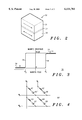
- FIG. 1 shows a memory bank circuit and other peripheral circuits in an MRAM device
- FIG. 2 shows a simplified and enlarged magnetic memory cell with magnetic layers separated by a non-magnetic layer
- FIG. 3 shows a graph illustrating hysteresis characteristics of the magnetic memory cell described in FIG. 2;
- FIG. 4 shows another embodiment for an MRAM element circuit
- FIG. 5 shows an entire MRAM device circuit having four memory banks.
- FIG. 1 shows a memory bank circuit 10 and other peripheral circuits including a bit/reference line selector 11, a digit line control 12, a selector 13, and a comparator circuit 14. These circuits are fabricated on a semiconductor or a glass substrate. Although one memory bank is illustrated in FIG. 1, it should be understood that an MRAM device includes a plurality of memory banks for more memory capacity, which will be described hereinafter with reference to FIG. 5.
- Memory bank 10 has magnetic memory cells (memory cells) 15-18 and reference memory cells 19 and 20. Memory cells 15-18 are placed on intersections of sense or bit lines 21-24 and torque or digit lines 25 and 26 perpendicular to bit lines 21-24, while reference memory cells (reference cells) 19 and 20 are placed on intersections of a reference line 27 and digit lines 25 and 26. Memory cells 15-18 and reference cells 19 and 20 form the same cell structure as illustrated in FIG. 3, the details of which will be discussed hereinafter. Memory cells 15-18 and reference cells 19 and 20 are coupled in series to transistors 28-32, which control a current flow in memory cells 15-18 and reference cells 19 and 20 to a ground or common line 33. As can be seen in FIG. 1, memory bank 10 has a single reference line and four bit lines.
- memory bank 10 includes two bit lines on both sides of the reference line, furthermore it is possible to add other bit lines for enlargement of the memory capacity.
- Bit lines 21-24 and reference line 27 are coupled to switching transistors 34-38 that selector 11 manages so as to provide a sense current and a reference current, respectively.
- Digit line control 12 places digit lines 25 and 26 adjacent the memory cells, and couples lines 39-40 to transistors 28-32.
- Transistors 41 and 42 in response to a signal on terminal 43, couple bit lines 21 and 23 to non-inverting inputs 44 and 45 of comparators 46 and 47, while transistors 48 and 49, in response to a signal on terminal 50, couple bit lines 22 and 24 to non-inverting inputs 44 and 45 of comparators 46 and 47 as well.
- Transistor 51 controlled by a signal on a terminal 52 couples reference line 27 to inverting inputs 53 and 54 of comparators 46 and 47.
- Comparators 46 and 47 compare voltages on non-inverting inputs 44 and 45 to reference voltage on inverting inputs 53 and 54 to produce output signals O 0 and O 1 on output terminals 55 and 56.
- selector 11 sends turn-on signals to gate electrodes of transistors 34 and 36 and transistor 38 to activate bit lines 21 and 23 and reference line 27, respectively.
- line control 12 provides a turn-on signal on line 39 to allow transistors 28-32 to turn on. Consequently, a sense current Is, indicated by an arrow 57, flows from a power line 58 through transistor 34, target cell 15 and transistor 28 to common line 33 while a sense current Is', indicated by an arrow 59, flows from power line 58 through transistor 36, target cell 17 and transistor 30 to common line 33.
- a reference current Ir expressed by an arrow 60 is supplied from power line 58 through transistor 38, reference cell 19 and transistor 32 to common line 33.
- Sense currents Is and Is' generate voltage drops across target cells 15 and 17 that are introduced to non-inverting inputs 44 and 45 of comparators 46 and 47 after turning transistors 41 and 42 on.
- reference current Ir produces a voltage drop across reference cell 19 that is conducted through transistor 51 to both inverting inputs 53 and 54 of comparators 46 and 47.
- Comparators 46 and 47 compare voltage values on non-inverting and inverting inputs. Comparator 46, for instance, provides a high-voltage signal on output terminal 55 when the voltage drop across target cell 15 is higher than the reference cell 19; otherwise a low-voltage appears on output terminal 55.
- a gate voltage applied to transistor 38 from line selector 11 controls reference current Ir. Assuming a magnetic memory cell produces a maximum voltage Vmax at an Anti-parallel state and a minimum voltage Vmin at a Parallel state, reference current Ir adjusts a reference voltage Vref generated across a reference magnetic cell so as to have a half voltage between Vmax and Vmin; that is,
- line selector 11 turns on transistor 61 and a turn-on signal is provided on terminal 43 to turn transistor 41 on, which allows bit line 21 to activate.
- a bit line program control 62 turns on transistor 63.
- bit current Ib indicated by an arrow 64 flows from power line 58 through transistor 61, bit line 21, transistor 41, and transistor 63, to common line 33.
- line control 12 activates digit line 25 to provide digit current Id indicated by an arrow 65.
- Bit current Ib and digit current Id generate magnetic fields, respectively. These magnetic fields are combined toward target cell 15.
- digit line control 12 manages the directions of digit current Id. During a program mode, digit line control 12 pulls down lines 39 and 40, turning off transistors 28-32. Also comparators 46 and 47 are disabled, and no current flows through reference line 23 during a program mode.
- FIGS. 2 and 3 show an isometric view of a simplified and enlarged memory cell structure 70 and hysteresis characteristics 75 of memory cell 70 in FIG. 2. It should be noted that other types of magnetic memory cells can be employed for the memory device.
- Memory cell 70 has three layers that include first and second magnetic layers 71 and 72 separated by a non-magnetic layer 73.
- First and second magnetic layers 71 and 72 use magnetic material such as CoFe and NiFeCo, respectively.
- Magnetization vectors in first magnetic layer 71 for example, are magnetically pinned by an antiferromagnetic layer (not shown) that is placed adjacent layer 71.
- Second magnetic layer 72 which is magnetically free, alternates magnetization vectors responding to an external magnetic field.
- Non-magnetic layer 73 for example, is formed by an insulating material such as A1 2 O 3 and has a thickness of around 30 ⁇ . The thin thickness allows non-magnetic layer 73 to form a tunneling junction between first and second magnetic layers 71 and 72, through which a tunneling current flows. As will be seen in FIG. 3, a magnetic resistance of the memory cell changes according to directions of magnetization in second magnetic layer 72 that causes a tunneling current in non-magnetic layer 73 to vary. 15 The magnetic layers would be patterned to substantially align the magnetization as shown in U.S. Pat. No. 5,757,695.
- the abscissa of FIG. 3 indicates a direction and strength of a magnetic field applied to memory cell 70.
- the ordinate represents the magnetic resistance of the memory cell 70.
- the external magnetic field changes to a value Hi moving to the right along the abscissa.
- curve 76 magnetization vectors in second magnetic (free) layer 72 are switched to the left at a magnetic field Hi and magnetization vectors in layers 71 and 72 are oriented in the Anti-parallel state (opposite direction) as indicated by arrows 77.
- FIG. 4 another embodiment of an array 80 of cells similar to cell 70 in FIG. 2 is illustrated with the cells being oriented in rows and columns. Only four cells 81 through 84 are illustrated for convenience, but it will be understood that any desired number of cells which can be practically fabricated can be employed.
- a plurality of diodes 85 through 88 are supplied, one each being associated with each cell 81 through 84.
- one terminal of the associated diode is connected to the lower or upper magnetic layer of the associated cell by means of an electrically conductive portion, which may include material such as a conductive layer, or solder, or the diodes may be integrated into a substrate or upper layer and formed with the conductive portion as a portion of the diode.
- a second terminal of the diode is connected to a sense line and the other of the first and second magnetic layers of the cell are connected to a word line as shown in U.S. Pat. No. 5,734,605.
- cell 81 has a magnetic layer connected to one terminal of diode 85 and the other magnetic layer connected to a bit line Bo.
- the second terminal of diode 85 is connected to a word line W 0 .
- word line W 0 Any change in resistance of cell 81 can be easily and quickly sensed by connecting sensing apparatus between bit line B 0 and word line W 0 .
- diode 85 is forward biased. Once diode 85 is forward biased, current flows from bit line B 0 through cell 81 and diode 85 to word line W 0 . All other diodes 86-88 are reverse biased. As a result, no current flows through cell 82-84.
- FIG. 5 shows an entire MRAM circuit 90 that includes memory banks 91-94, a bit/reference line control 95, digit line control 96, selector 97, and a comparator circuit 98. These circuits are fabricated on a semiconductor or a glass substrate. MRAM circuit 90 has four memory banks 91-94. It should be noted that more memory banks are established upon request of more memory capacity. Only memory bank 91 will be discussed hereinafter because memory banks 92-94 have the same circuit structure and operation as memory bank 91.
- Memory bank 91 includes one reference line sR.LINE0, and one hundred twenty eight bit lines B.LINE0-B.LINE127 that are divided into four groups, that is, first group for bit lines B.LINE0-B.LINE31, second group for bit lines B.LINE32-B.LINE63, third group for bit lines B.LINE64-B.LINE95, and fourth group for bit lines B.LINE96-B.LINE127.
- First and second groups and third and fourth groups are symmetrically and physically allocated on both sides of reference line R.LINE0 on a substrate.
- Magnetic memory cells are arrayed on intersections of bit lines B.LINE0-B.LINE127 and digit lines D.LINE0-D.LINE N while reference magnetic memory cells are placed on intersections of reference line R.LINEO and digit lines D.LINE0-D.LINE N.
- Each memory cell for instance, a cell 101 is coupled to a transistor 105 that, in response to a signal on a word line W.LINEO, switches on and off a sense current supplied from bit line B.LINE0 to cell 101.
- transistor 105 is replaceable with a diode.
- one bit line in each group is selected and activated to read magnetic states in a target cell.
- line control 95 selects bit lines B.LINE0 in the first group, B.LINE32 in the second group, B.LINE64 in the third group, and B.LINE96 in the fourth group, and at the same time line control 96 sends a turn-on signal on word line W.LINE0.
- target cells 101-104 are activated to provide sense currents therein, respectively.
- line control 95 supplies a reference current into reference line R.LINE0 to generate a reference voltage across a reference memory cell 106. Voltage drops across target cells 101-104 and the reference voltage are applied to comparators 111-114 through selector 97.
- a voltage drop across target cell 101 is introduced to selector 97 by way of bit line B.LINE0, while the reference voltage is provided to selector 97 through reference line R.LINE0.
- Selector 97 connects bit line B.LINE0 and reference line R.LINE0 to non-inverting input 115 and inverting input 116 of comparator 111, respectively.
- Comparator 111 finally evaluates voltages at both inputs to set an output signal O 0 at an output terminal 117.
- second, third, and fourth groups works as well as the above for the first group, that allows comparators 118-119 to provide output signals O 1 -O 3 at output terminal 118-120, respectively.
- memory banks 92-94 operate in the same function as memory bank 91, as a result output signals O 4 -O 15 are furnished. Accordingly, memory device 90, which has four memory banks, each bank including four groups, simultaneously provides sixteen outputs.
- a new and improved MRAM device which allocates memory banks on a substrate, each memory bank including bit lines and a reference line on which magnetic memory cells and reference memory cells are arrayed. These cells have very thin layers. In generally, it is very hard to uniformly control the width of layers over the entire substrate in order for all the cells to have the same hysteresis characteristic curves.
- bit lines are placed on both sides of the reference line in each memory bank. This feature provides a steady reading function because a target cell that is close to a reference cell is selected and activated, and both cells have substantially the same hysteresis characteristics.
Landscapes
- Engineering & Computer Science (AREA)
- Computer Hardware Design (AREA)
- Mram Or Spin Memory Techniques (AREA)
- Semiconductor Memories (AREA)
- Hall/Mr Elements (AREA)
Abstract
Description
Vref=(Vmax+Vmin)/2
Claims (9)
Priority Applications (7)
| Application Number | Priority Date | Filing Date | Title |
|---|---|---|---|
| US09/128,020 US6111781A (en) | 1998-08-03 | 1998-08-03 | Magnetic random access memory array divided into a plurality of memory banks |
| DE69930129T DE69930129T2 (en) | 1998-08-03 | 1999-08-03 | MRAM MEMORY WITH MULTIPLE MEMORY BANKS |
| PCT/US1999/017581 WO2000008650A1 (en) | 1998-08-03 | 1999-08-03 | Mram array having a plurality of memory banks |
| EP99937766A EP1105879B1 (en) | 1998-08-03 | 1999-08-03 | Mram array having a plurality of memory banks |
| JP2000564205A JP4574010B2 (en) | 1998-08-03 | 1999-08-03 | MRAM array having a plurality of memory banks |
| TW088113174A TW454185B (en) | 1998-08-03 | 1999-11-16 | Magnetic random access memory array divided into a plurality of memory banks |
| US09/568,822 US6278631B1 (en) | 1998-08-03 | 2000-05-10 | Magnetic random access memory array divided into a plurality of memory banks |
Applications Claiming Priority (1)
| Application Number | Priority Date | Filing Date | Title |
|---|---|---|---|
| US09/128,020 US6111781A (en) | 1998-08-03 | 1998-08-03 | Magnetic random access memory array divided into a plurality of memory banks |
Related Child Applications (1)
| Application Number | Title | Priority Date | Filing Date |
|---|---|---|---|
| US09/568,822 Division US6278631B1 (en) | 1998-08-03 | 2000-05-10 | Magnetic random access memory array divided into a plurality of memory banks |
Publications (1)
| Publication Number | Publication Date |
|---|---|
| US6111781A true US6111781A (en) | 2000-08-29 |
Family
ID=22433205
Family Applications (2)
| Application Number | Title | Priority Date | Filing Date |
|---|---|---|---|
| US09/128,020 Expired - Lifetime US6111781A (en) | 1998-08-03 | 1998-08-03 | Magnetic random access memory array divided into a plurality of memory banks |
| US09/568,822 Expired - Lifetime US6278631B1 (en) | 1998-08-03 | 2000-05-10 | Magnetic random access memory array divided into a plurality of memory banks |
Family Applications After (1)
| Application Number | Title | Priority Date | Filing Date |
|---|---|---|---|
| US09/568,822 Expired - Lifetime US6278631B1 (en) | 1998-08-03 | 2000-05-10 | Magnetic random access memory array divided into a plurality of memory banks |
Country Status (6)
| Country | Link |
|---|---|
| US (2) | US6111781A (en) |
| EP (1) | EP1105879B1 (en) |
| JP (1) | JP4574010B2 (en) |
| DE (1) | DE69930129T2 (en) |
| TW (1) | TW454185B (en) |
| WO (1) | WO2000008650A1 (en) |
Cited By (44)
| Publication number | Priority date | Publication date | Assignee | Title |
|---|---|---|---|---|
| EP1003176A2 (en) * | 1998-11-19 | 2000-05-24 | Infineon Technologies AG | Magnetic memory |
| EP1126468A2 (en) * | 2000-02-04 | 2001-08-22 | Hewlett-Packard Company, A Delaware Corporation | MRAM device including differential sense amplifiers |
| US6317376B1 (en) * | 2000-06-20 | 2001-11-13 | Hewlett-Packard Company | Reference signal generation for magnetic random access memory devices |
| US6335890B1 (en) * | 2000-11-01 | 2002-01-01 | International Business Machines Corporation | Segmented write line architecture for writing magnetic random access memories |
| EP1205937A2 (en) * | 2000-11-09 | 2002-05-15 | Sanyo Electric Co., Ltd. | Magnetic memory device including storage element exhibiting ferromagnetic tunnel effect |
| US6426907B1 (en) | 2001-01-24 | 2002-07-30 | Infineon Technologies North America Corp. | Reference for MRAM cell |
| US20020172068A1 (en) * | 2001-05-16 | 2002-11-21 | Mitsubishi Denki Kabushiki Kaisha | Thin film magnetic memory device having a magnetic tunnel junction |
| US6515896B1 (en) * | 2001-07-24 | 2003-02-04 | Hewlett-Packard Company | Memory device with short read time |
| US6545900B2 (en) * | 2000-09-12 | 2003-04-08 | Infineon Technologies, Ag | MRAM module configuration |
| WO2003052828A1 (en) * | 2001-12-14 | 2003-06-26 | Hitachi, Ltd. | Semiconductor device |
| US6587370B2 (en) * | 2000-11-01 | 2003-07-01 | Canon Kabushiki Kaisha | Magnetic memory and information recording and reproducing method therefor |
| US6608776B2 (en) * | 2000-11-14 | 2003-08-19 | Mitsubishi Denki Kabushiki Kaisha | Thin film magnetic memory device having a highly integrated memory array |
| US6667899B1 (en) | 2003-03-27 | 2003-12-23 | Motorola, Inc. | Magnetic memory and method of bi-directional write current programming |
| US20040001358A1 (en) * | 2002-06-28 | 2004-01-01 | Nahas Joseph J. | MRAM architecture with electrically isolated read and write circuitry |
| US6693824B2 (en) | 2002-06-28 | 2004-02-17 | Motorola, Inc. | Circuit and method of writing a toggle memory |
| US20040042262A1 (en) * | 2002-09-03 | 2004-03-04 | Tran Lung T. | Memory device capable of calibration and calibration methods therefor |
| US20040065906A1 (en) * | 2002-08-12 | 2004-04-08 | Yoshiaki Asao | Semiconductor integrated circuit device |
| US6753561B1 (en) | 2002-08-02 | 2004-06-22 | Unity Semiconductor Corporation | Cross point memory array using multiple thin films |
| US6760244B2 (en) | 2002-01-30 | 2004-07-06 | Sanyo Electric Co., Ltd. | Magnetic memory device including storage elements exhibiting a ferromagnetic tunnel effect |
| US20040160818A1 (en) * | 2002-08-02 | 2004-08-19 | Unity Semiconductor Corporation | Cross point memory array using multiple modes of operation |
| US20040160819A1 (en) * | 2002-08-02 | 2004-08-19 | Unity Semiconductor Corporation | High-density NVRAM |
| US20040160805A1 (en) * | 2002-08-02 | 2004-08-19 | Unity Semiconductor Corporation | Multi-output multiplexor |
| US20040160808A1 (en) * | 2002-08-02 | 2004-08-19 | Unity Semiconductor Corporation | Cross point memory array using distinct voltages |
| US20040160806A1 (en) * | 2002-08-02 | 2004-08-19 | Unity Semiconductor Corporation | Providing a reference voltage to a cross point memory array |
| US20040160807A1 (en) * | 2002-08-02 | 2004-08-19 | Unity Semiconductor Corporation | Cross point memory array with memory plugs exhibiting a characteristic hysteresis |
| US20040160804A1 (en) * | 2002-08-02 | 2004-08-19 | Unity Semiconductor Corporation | Memory array of a non-volatile ram |
| US20040160841A1 (en) * | 2002-08-02 | 2004-08-19 | Darrell Rinerson | Multiplexor having a reference voltage on unselected lines |
| US20040160817A1 (en) * | 2002-08-02 | 2004-08-19 | Unity Semiconductor Corporation | Non-volatile memory with a single transistor and resistive memory element |
| US6822895B2 (en) | 2001-06-06 | 2004-11-23 | Sanyo Electric Co., Ltd. | Magnetic memory device |
| US6873547B1 (en) * | 2001-02-23 | 2005-03-29 | Read Rite Corporation | High capacity MRAM memory array architecture |
| US20060018149A1 (en) * | 2004-07-20 | 2006-01-26 | Unity Semiconductor Corporation | Two terminal memory array having reference cells |
| US20060164882A1 (en) * | 2004-12-23 | 2006-07-27 | Robert Norman | Storage controller using vertical memory |
| US20090067233A1 (en) * | 2003-12-30 | 2009-03-12 | Samsung Electronics Co., Ltd. | Magnetic random access memory and method of reading data from the same |
| US20090233576A1 (en) * | 2000-12-29 | 2009-09-17 | Vesta Corporation | Toll free calling account recharge system and method |
| CN1735942B (en) * | 2003-01-17 | 2010-06-09 | 爱沃斯宾技术公司 | MRAM architecture with a grounded write bit line and electrically isolated read bit line |
| US20100277975A1 (en) * | 2009-04-30 | 2010-11-04 | Sung-Yeon Lee | Semiconductor memory device |
| US20120069643A1 (en) * | 2006-10-20 | 2012-03-22 | Avalanche Technology, Inc. | Non-uniform switching based non-volatile magnetic based memory |
| US20120069644A1 (en) * | 2010-09-22 | 2012-03-22 | Magic Technologies, Inc. | Replaceable, precise-tracking reference lines for memory products |
| US8750018B2 (en) | 2012-06-04 | 2014-06-10 | Samsung Electronics Co., Ltd. | Sense amplifier circuitry for resistive type memory |
| US9070424B2 (en) | 2012-06-29 | 2015-06-30 | Samsung Electronics Co., Ltd. | Sense amplifier circuitry for resistive type memory |
| US9183910B2 (en) | 2012-05-31 | 2015-11-10 | Samsung Electronics Co., Ltd. | Semiconductor memory devices for alternately selecting bit lines |
| US9431083B2 (en) | 2014-03-25 | 2016-08-30 | Samsung Electronics Co., Ltd. | Nonvolatile memory device and storage device having the same |
| US20220199181A1 (en) * | 2020-12-18 | 2022-06-23 | Ememory Technology Inc. | Memory device having reference memory array structure resembling data memory array structure, and methods of operating the same |
| US12205633B2 (en) * | 2022-06-14 | 2025-01-21 | Globalfoundries U.S. Inc. | Non-volatile memory device with reference voltage circuit including column(s) of reference bit cells adjacent columns of memory bit cells within a memory cell array |
Families Citing this family (33)
| Publication number | Priority date | Publication date | Assignee | Title |
|---|---|---|---|---|
| US6256224B1 (en) * | 2000-05-03 | 2001-07-03 | Hewlett-Packard Co | Write circuit for large MRAM arrays |
| US6244331B1 (en) * | 1999-10-22 | 2001-06-12 | Intel Corporation | Heatsink with integrated blower for improved heat transfer |
| JP4477199B2 (en) * | 2000-06-16 | 2010-06-09 | 株式会社ルネサステクノロジ | Magnetic random access memory, method for accessing magnetic random access memory, and method for manufacturing magnetic random access memory |
| US6331943B1 (en) * | 2000-08-28 | 2001-12-18 | Motorola, Inc. | MTJ MRAM series-parallel architecture |
| US6272041B1 (en) * | 2000-08-28 | 2001-08-07 | Motorola, Inc. | MTJ MRAM parallel-parallel architecture |
| JP2002170377A (en) * | 2000-09-22 | 2002-06-14 | Mitsubishi Electric Corp | Thin film magnetic storage device |
| JP2002100181A (en) * | 2000-09-27 | 2002-04-05 | Nec Corp | Magnetic ramdom access memory |
| JP4149647B2 (en) * | 2000-09-28 | 2008-09-10 | 株式会社東芝 | Semiconductor memory device and manufacturing method thereof |
| JP4577334B2 (en) * | 2000-11-27 | 2010-11-10 | 株式会社日立製作所 | Semiconductor device |
| JP4667594B2 (en) | 2000-12-25 | 2011-04-13 | ルネサスエレクトロニクス株式会社 | Thin film magnetic memory device |
| JP3920565B2 (en) * | 2000-12-26 | 2007-05-30 | 株式会社東芝 | Magnetic random access memory |
| JP4712204B2 (en) * | 2001-03-05 | 2011-06-29 | ルネサスエレクトロニクス株式会社 | Storage device |
| JP5355666B2 (en) * | 2001-04-26 | 2013-11-27 | ルネサスエレクトロニクス株式会社 | Thin film magnetic memory device |
| JP4434527B2 (en) * | 2001-08-08 | 2010-03-17 | 株式会社東芝 | Semiconductor memory device |
| US6829158B2 (en) * | 2001-08-22 | 2004-12-07 | Motorola, Inc. | Magnetoresistive level generator and method |
| US6869855B1 (en) | 2001-09-02 | 2005-03-22 | Borealis Technical Limited | Method for making electrode pairs |
| JP4780874B2 (en) * | 2001-09-04 | 2011-09-28 | ルネサスエレクトロニクス株式会社 | Thin film magnetic memory device |
| JP3853199B2 (en) * | 2001-11-08 | 2006-12-06 | Necエレクトロニクス株式会社 | Semiconductor memory device and method for reading semiconductor memory device |
| JP2003197872A (en) * | 2001-12-26 | 2003-07-11 | Canon Inc | Memory using magneto-resistance effect film |
| AU2003201760A1 (en) | 2002-04-04 | 2003-10-20 | Kabushiki Kaisha Toshiba | Phase-change memory device |
| JP4282314B2 (en) * | 2002-06-25 | 2009-06-17 | シャープ株式会社 | Storage device |
| KR100496858B1 (en) * | 2002-08-02 | 2005-06-22 | 삼성전자주식회사 | Magnetic random access memory for flowing constant(I(H)+I(L))/2) current to reference cell without regard of bitline clamp voltage |
| KR100506932B1 (en) * | 2002-12-10 | 2005-08-09 | 삼성전자주식회사 | Magnetic random access memory device having reference cells and structure thereof |
| JP3766380B2 (en) * | 2002-12-25 | 2006-04-12 | 株式会社東芝 | Magnetic random access memory and data read method of the magnetic random access memory |
| US7123530B2 (en) * | 2003-10-09 | 2006-10-17 | Micron Technology, Inc. | AC sensing for a resistive memory |
| JP4675362B2 (en) * | 2007-08-10 | 2011-04-20 | ルネサスエレクトロニクス株式会社 | Semiconductor device |
| JP4712779B2 (en) * | 2007-10-19 | 2011-06-29 | ルネサスエレクトロニクス株式会社 | Thin film magnetic memory device |
| JP2008084533A (en) * | 2007-11-09 | 2008-04-10 | Renesas Technology Corp | Thin magnetic film storage device |
| JP5165040B2 (en) * | 2010-10-15 | 2013-03-21 | ルネサスエレクトロニクス株式会社 | Semiconductor integrated circuit |
| JP5138056B2 (en) * | 2011-03-03 | 2013-02-06 | ルネサスエレクトロニクス株式会社 | Thin film magnetic memory device |
| JP5213980B2 (en) * | 2011-03-23 | 2013-06-19 | ルネサスエレクトロニクス株式会社 | Thin film magnetic memory device |
| JP5192566B2 (en) * | 2011-05-27 | 2013-05-08 | ルネサスエレクトロニクス株式会社 | Thin film magnetic memory device |
| KR102116719B1 (en) * | 2013-12-24 | 2020-05-29 | 삼성전자 주식회사 | Magnetic memory device |
Citations (5)
| Publication number | Priority date | Publication date | Assignee | Title |
|---|---|---|---|---|
| US5173873A (en) * | 1990-06-28 | 1992-12-22 | The United States Of America As Represented By The Administrator Of The National Aeronautics And Space Administration | High speed magneto-resistive random access memory |
| EP0613148A2 (en) * | 1993-02-23 | 1994-08-31 | International Business Machines Corporation | Nonvolatile magnetoresistive storage device |
| US5831920A (en) * | 1997-10-14 | 1998-11-03 | Motorola, Inc. | GMR device having a sense amplifier protected by a circuit for dissipating electric charges |
| US5894447A (en) * | 1996-09-26 | 1999-04-13 | Kabushiki Kaisha Toshiba | Semiconductor memory device including a particular memory cell block structure |
| US5946227A (en) * | 1998-07-20 | 1999-08-31 | Motorola, Inc. | Magnetoresistive random access memory with shared word and digit lines |
Family Cites Families (4)
| Publication number | Priority date | Publication date | Assignee | Title |
|---|---|---|---|---|
| JP2845952B2 (en) * | 1989-06-28 | 1999-01-13 | 株式会社日立製作所 | Thin film magnetic memory cell and its recording and reproducing apparatus |
| JPH0512891A (en) * | 1990-09-17 | 1993-01-22 | Toshiba Corp | Semiconductor storage |
| KR100224673B1 (en) * | 1996-12-13 | 1999-10-15 | 윤종용 | Non-volatile ferroelectric memory device and driving method thereof |
| US6055178A (en) * | 1998-12-18 | 2000-04-25 | Motorola, Inc. | Magnetic random access memory with a reference memory array |
-
1998
- 1998-08-03 US US09/128,020 patent/US6111781A/en not_active Expired - Lifetime
-
1999
- 1999-08-03 JP JP2000564205A patent/JP4574010B2/en not_active Expired - Lifetime
- 1999-08-03 DE DE69930129T patent/DE69930129T2/en not_active Expired - Fee Related
- 1999-08-03 WO PCT/US1999/017581 patent/WO2000008650A1/en active IP Right Grant
- 1999-08-03 EP EP99937766A patent/EP1105879B1/en not_active Expired - Lifetime
- 1999-11-16 TW TW088113174A patent/TW454185B/en not_active IP Right Cessation
-
2000
- 2000-05-10 US US09/568,822 patent/US6278631B1/en not_active Expired - Lifetime
Patent Citations (5)
| Publication number | Priority date | Publication date | Assignee | Title |
|---|---|---|---|---|
| US5173873A (en) * | 1990-06-28 | 1992-12-22 | The United States Of America As Represented By The Administrator Of The National Aeronautics And Space Administration | High speed magneto-resistive random access memory |
| EP0613148A2 (en) * | 1993-02-23 | 1994-08-31 | International Business Machines Corporation | Nonvolatile magnetoresistive storage device |
| US5894447A (en) * | 1996-09-26 | 1999-04-13 | Kabushiki Kaisha Toshiba | Semiconductor memory device including a particular memory cell block structure |
| US5831920A (en) * | 1997-10-14 | 1998-11-03 | Motorola, Inc. | GMR device having a sense amplifier protected by a circuit for dissipating electric charges |
| US5946227A (en) * | 1998-07-20 | 1999-08-31 | Motorola, Inc. | Magnetoresistive random access memory with shared word and digit lines |
Cited By (80)
| Publication number | Priority date | Publication date | Assignee | Title |
|---|---|---|---|---|
| EP1003176A3 (en) * | 1998-11-19 | 2001-01-03 | Infineon Technologies AG | Magnetic memory |
| US6359829B1 (en) | 1998-11-19 | 2002-03-19 | Infineon Technologies Ag | Magnetic memory |
| EP1003176A2 (en) * | 1998-11-19 | 2000-05-24 | Infineon Technologies AG | Magnetic memory |
| EP1126468A2 (en) * | 2000-02-04 | 2001-08-22 | Hewlett-Packard Company, A Delaware Corporation | MRAM device including differential sense amplifiers |
| EP1126468A3 (en) * | 2000-02-04 | 2001-09-19 | Hewlett-Packard Company, A Delaware Corporation | MRAM device including differential sense amplifiers |
| US6317376B1 (en) * | 2000-06-20 | 2001-11-13 | Hewlett-Packard Company | Reference signal generation for magnetic random access memory devices |
| US6385111B2 (en) * | 2000-06-20 | 2002-05-07 | Hewlett-Packard Company | Reference signal generation for magnetic random access memory devices |
| US6545900B2 (en) * | 2000-09-12 | 2003-04-08 | Infineon Technologies, Ag | MRAM module configuration |
| US6335890B1 (en) * | 2000-11-01 | 2002-01-01 | International Business Machines Corporation | Segmented write line architecture for writing magnetic random access memories |
| US6587370B2 (en) * | 2000-11-01 | 2003-07-01 | Canon Kabushiki Kaisha | Magnetic memory and information recording and reproducing method therefor |
| EP1205937A2 (en) * | 2000-11-09 | 2002-05-15 | Sanyo Electric Co., Ltd. | Magnetic memory device including storage element exhibiting ferromagnetic tunnel effect |
| EP1205937A3 (en) * | 2000-11-09 | 2003-04-09 | Sanyo Electric Co., Ltd. | Magnetic memory device including storage element exhibiting ferromagnetic tunnel effect |
| US6608776B2 (en) * | 2000-11-14 | 2003-08-19 | Mitsubishi Denki Kabushiki Kaisha | Thin film magnetic memory device having a highly integrated memory array |
| US7505305B2 (en) * | 2000-11-14 | 2009-03-17 | Renesas Technology Corp. | Thin film magnetic memory device having a highly integrated memory array |
| US6975534B2 (en) | 2000-11-14 | 2005-12-13 | Renesas Technology Corp. | Thin film magnetic memory device having a highly integrated memory array |
| US20060056236A1 (en) * | 2000-11-14 | 2006-03-16 | Renesas Technology Corp. | Thin film magnetic memory device having a highly integrated memory array |
| US7133310B2 (en) | 2000-11-14 | 2006-11-07 | Renesas Technology Corp. | Thin film magnetic memory device having a highly integrated memory array |
| US20070091670A1 (en) * | 2000-11-14 | 2007-04-26 | Renesas Technology Corp. | Thin film magnetic memory device having a highly integrated memory array |
| US20090154225A1 (en) * | 2000-11-14 | 2009-06-18 | Renesas Technology Corp | Thin film magnetic memory device having a highly integrated memory array |
| US20040047196A1 (en) * | 2000-11-14 | 2004-03-11 | Mitsubishi Denki Kabushiki Kaisha | Thin film magnetic memory device having a highly integrated memory array |
| US7719885B2 (en) | 2000-11-14 | 2010-05-18 | Renesas Technology Corp. | Thin film magnetic memory device having a highly integrated memory array |
| US20090233576A1 (en) * | 2000-12-29 | 2009-09-17 | Vesta Corporation | Toll free calling account recharge system and method |
| US7979051B2 (en) | 2000-12-29 | 2011-07-12 | Vesta Corporation | Toll free calling account recharge system and method |
| US6426907B1 (en) | 2001-01-24 | 2002-07-30 | Infineon Technologies North America Corp. | Reference for MRAM cell |
| US6873547B1 (en) * | 2001-02-23 | 2005-03-29 | Read Rite Corporation | High capacity MRAM memory array architecture |
| US6876575B2 (en) | 2001-05-16 | 2005-04-05 | Renesas Technology Corp. | Thin film magnetic memory device having a magnetic tunnel junction |
| US7116595B2 (en) | 2001-05-16 | 2006-10-03 | Renesas Technology Corp. | Thin film magnetic memory device having a magnetic tunnel junction |
| US20020172068A1 (en) * | 2001-05-16 | 2002-11-21 | Mitsubishi Denki Kabushiki Kaisha | Thin film magnetic memory device having a magnetic tunnel junction |
| US6822895B2 (en) | 2001-06-06 | 2004-11-23 | Sanyo Electric Co., Ltd. | Magnetic memory device |
| US6515896B1 (en) * | 2001-07-24 | 2003-02-04 | Hewlett-Packard Company | Memory device with short read time |
| WO2003052828A1 (en) * | 2001-12-14 | 2003-06-26 | Hitachi, Ltd. | Semiconductor device |
| US6760244B2 (en) | 2002-01-30 | 2004-07-06 | Sanyo Electric Co., Ltd. | Magnetic memory device including storage elements exhibiting a ferromagnetic tunnel effect |
| US20040001358A1 (en) * | 2002-06-28 | 2004-01-01 | Nahas Joseph J. | MRAM architecture with electrically isolated read and write circuitry |
| US6903964B2 (en) | 2002-06-28 | 2005-06-07 | Freescale Semiconductor, Inc. | MRAM architecture with electrically isolated read and write circuitry |
| US20050152183A1 (en) * | 2002-06-28 | 2005-07-14 | Nahas Joseph J. | MRAM architecture with electrically isolated read and write circuitry |
| US7154772B2 (en) | 2002-06-28 | 2006-12-26 | Freescale Semiconductor, Inc. | MRAM architecture with electrically isolated read and write circuitry |
| US6693824B2 (en) | 2002-06-28 | 2004-02-17 | Motorola, Inc. | Circuit and method of writing a toggle memory |
| US6850455B2 (en) | 2002-08-02 | 2005-02-01 | Unity Semiconductor Corporation | Multiplexor having a reference voltage on unselected lines |
| US20040160819A1 (en) * | 2002-08-02 | 2004-08-19 | Unity Semiconductor Corporation | High-density NVRAM |
| US20050013172A1 (en) * | 2002-08-02 | 2005-01-20 | Darrell Rinerson | Multiple modes of operation in a cross point array |
| US6831854B2 (en) | 2002-08-02 | 2004-12-14 | Unity Semiconductor Corporation | Cross point memory array using distinct voltages |
| US6856536B2 (en) | 2002-08-02 | 2005-02-15 | Unity Semiconductor Corporation | Non-volatile memory with a single transistor and resistive memory element |
| US6859382B2 (en) | 2002-08-02 | 2005-02-22 | Unity Semiconductor Corporation | Memory array of a non-volatile ram |
| US6798685B2 (en) | 2002-08-02 | 2004-09-28 | Unity Semiconductor Corporation | Multi-output multiplexor |
| US6753561B1 (en) | 2002-08-02 | 2004-06-22 | Unity Semiconductor Corporation | Cross point memory array using multiple thin films |
| US20040160817A1 (en) * | 2002-08-02 | 2004-08-19 | Unity Semiconductor Corporation | Non-volatile memory with a single transistor and resistive memory element |
| US6909632B2 (en) | 2002-08-02 | 2005-06-21 | Unity Semiconductor Corporation | Multiple modes of operation in a cross point array |
| US6917539B2 (en) | 2002-08-02 | 2005-07-12 | Unity Semiconductor Corporation | High-density NVRAM |
| US20040160841A1 (en) * | 2002-08-02 | 2004-08-19 | Darrell Rinerson | Multiplexor having a reference voltage on unselected lines |
| US6970375B2 (en) | 2002-08-02 | 2005-11-29 | Unity Semiconductor Corporation | Providing a reference voltage to a cross point memory array |
| US20040160804A1 (en) * | 2002-08-02 | 2004-08-19 | Unity Semiconductor Corporation | Memory array of a non-volatile ram |
| US20040160818A1 (en) * | 2002-08-02 | 2004-08-19 | Unity Semiconductor Corporation | Cross point memory array using multiple modes of operation |
| US20040160807A1 (en) * | 2002-08-02 | 2004-08-19 | Unity Semiconductor Corporation | Cross point memory array with memory plugs exhibiting a characteristic hysteresis |
| US6834008B2 (en) | 2002-08-02 | 2004-12-21 | Unity Semiconductor Corporation | Cross point memory array using multiple modes of operation |
| US20040160805A1 (en) * | 2002-08-02 | 2004-08-19 | Unity Semiconductor Corporation | Multi-output multiplexor |
| US20040160806A1 (en) * | 2002-08-02 | 2004-08-19 | Unity Semiconductor Corporation | Providing a reference voltage to a cross point memory array |
| US20040160808A1 (en) * | 2002-08-02 | 2004-08-19 | Unity Semiconductor Corporation | Cross point memory array using distinct voltages |
| US20040065906A1 (en) * | 2002-08-12 | 2004-04-08 | Yoshiaki Asao | Semiconductor integrated circuit device |
| US6791865B2 (en) | 2002-09-03 | 2004-09-14 | Hewlett-Packard Development Company, L.P. | Memory device capable of calibration and calibration methods therefor |
| US20040042262A1 (en) * | 2002-09-03 | 2004-03-04 | Tran Lung T. | Memory device capable of calibration and calibration methods therefor |
| CN1735942B (en) * | 2003-01-17 | 2010-06-09 | 爱沃斯宾技术公司 | MRAM architecture with a grounded write bit line and electrically isolated read bit line |
| US6667899B1 (en) | 2003-03-27 | 2003-12-23 | Motorola, Inc. | Magnetic memory and method of bi-directional write current programming |
| US8320166B2 (en) | 2003-12-30 | 2012-11-27 | Samsung Electronics Co., Ltd. | Magnetic random access memory and method of reading data from the same |
| US20090067233A1 (en) * | 2003-12-30 | 2009-03-12 | Samsung Electronics Co., Ltd. | Magnetic random access memory and method of reading data from the same |
| US7075817B2 (en) | 2004-07-20 | 2006-07-11 | Unity Semiconductor Corporation | Two terminal memory array having reference cells |
| US20060018149A1 (en) * | 2004-07-20 | 2006-01-26 | Unity Semiconductor Corporation | Two terminal memory array having reference cells |
| US7327600B2 (en) | 2004-12-23 | 2008-02-05 | Unity Semiconductor Corporation | Storage controller for multiple configurations of vertical memory |
| US20060164882A1 (en) * | 2004-12-23 | 2006-07-27 | Robert Norman | Storage controller using vertical memory |
| US20120069643A1 (en) * | 2006-10-20 | 2012-03-22 | Avalanche Technology, Inc. | Non-uniform switching based non-volatile magnetic based memory |
| US20100277975A1 (en) * | 2009-04-30 | 2010-11-04 | Sung-Yeon Lee | Semiconductor memory device |
| US8059480B2 (en) | 2009-04-30 | 2011-11-15 | Hynix Semiconductor Inc. | Semiconductor memory device |
| US20120069644A1 (en) * | 2010-09-22 | 2012-03-22 | Magic Technologies, Inc. | Replaceable, precise-tracking reference lines for memory products |
| US8605520B2 (en) * | 2010-09-22 | 2013-12-10 | Magic Technologies, Inc. | Replaceable, precise-tracking reference lines for memory products |
| US9183910B2 (en) | 2012-05-31 | 2015-11-10 | Samsung Electronics Co., Ltd. | Semiconductor memory devices for alternately selecting bit lines |
| US8750018B2 (en) | 2012-06-04 | 2014-06-10 | Samsung Electronics Co., Ltd. | Sense amplifier circuitry for resistive type memory |
| US9070424B2 (en) | 2012-06-29 | 2015-06-30 | Samsung Electronics Co., Ltd. | Sense amplifier circuitry for resistive type memory |
| US9431083B2 (en) | 2014-03-25 | 2016-08-30 | Samsung Electronics Co., Ltd. | Nonvolatile memory device and storage device having the same |
| US20220199181A1 (en) * | 2020-12-18 | 2022-06-23 | Ememory Technology Inc. | Memory device having reference memory array structure resembling data memory array structure, and methods of operating the same |
| US11749372B2 (en) * | 2020-12-18 | 2023-09-05 | Ememory Technology Inc. | Memory device having reference memory array structure resembling data memory array structure, and methods of operating the same |
| US12205633B2 (en) * | 2022-06-14 | 2025-01-21 | Globalfoundries U.S. Inc. | Non-volatile memory device with reference voltage circuit including column(s) of reference bit cells adjacent columns of memory bit cells within a memory cell array |
Also Published As
| Publication number | Publication date |
|---|---|
| EP1105879B1 (en) | 2006-03-01 |
| EP1105879A1 (en) | 2001-06-13 |
| DE69930129D1 (en) | 2006-04-27 |
| DE69930129T2 (en) | 2006-08-31 |
| JP4574010B2 (en) | 2010-11-04 |
| US6278631B1 (en) | 2001-08-21 |
| WO2000008650A1 (en) | 2000-02-17 |
| JP2002522864A (en) | 2002-07-23 |
| TW454185B (en) | 2001-09-11 |
Similar Documents
| Publication | Publication Date | Title |
|---|---|---|
| US6111781A (en) | Magnetic random access memory array divided into a plurality of memory banks | |
| US6055178A (en) | Magnetic random access memory with a reference memory array | |
| EP1018118B1 (en) | Mram with shared word and digit lines | |
| US5734605A (en) | Multi-layer magnetic tunneling junction memory cells | |
| US5640343A (en) | Magnetic memory array using magnetic tunnel junction devices in the memory cells | |
| US6812537B2 (en) | Magnetic memory and method of operation thereof | |
| US6781910B2 (en) | Small area magnetic memory devices | |
| US6483734B1 (en) | Memory device having memory cells capable of four states | |
| US5768181A (en) | Magnetic device having multi-layer with insulating and conductive layers | |
| US6211559B1 (en) | Symmetric magnetic tunnel device | |
| US6473337B1 (en) | Memory device having memory cells with magnetic tunnel junction and tunnel junction in series | |
| US7411815B2 (en) | Memory write circuit | |
| US6177204B1 (en) | Ferromagnetic GMR material and method of forming and using | |
| US7046547B2 (en) | Magnetic non-volatile memory coil layout architecture and process integration scheme | |
| US6477077B2 (en) | Non-volatile memory device | |
| EP1653516A2 (en) | Magneto-resistive RAM | |
| EP1573742A2 (en) | Magnetoresistive memory cell array and mram memory comprising such array | |
| US7075819B2 (en) | Closed flux magnetic memory | |
| US5838607A (en) | Spin polarized apparatus |
Legal Events
| Date | Code | Title | Description |
|---|---|---|---|
| AS | Assignment |
Owner name: MOTOROLA, INC., ILLINOIS Free format text: ASSIGNMENT OF ASSIGNORS INTEREST;ASSIGNOR:NAJI, PETER K.;REEL/FRAME:009364/0135 Effective date: 19980731 |
|
| STCF | Information on status: patent grant |
Free format text: PATENTED CASE |
|
| CC | Certificate of correction | ||
| FPAY | Fee payment |
Year of fee payment: 4 |
|
| AS | Assignment |
Owner name: FREESCALE SEMICONDUCTOR, INC., TEXAS Free format text: ASSIGNMENT OF ASSIGNORS INTEREST;ASSIGNOR:MOTOROLA, INC.;REEL/FRAME:015698/0657 Effective date: 20040404 Owner name: FREESCALE SEMICONDUCTOR, INC.,TEXAS Free format text: ASSIGNMENT OF ASSIGNORS INTEREST;ASSIGNOR:MOTOROLA, INC.;REEL/FRAME:015698/0657 Effective date: 20040404 |
|
| AS | Assignment |
Owner name: CITIBANK, N.A. AS COLLATERAL AGENT, NEW YORK Free format text: SECURITY AGREEMENT;ASSIGNORS:FREESCALE SEMICONDUCTOR, INC.;FREESCALE ACQUISITION CORPORATION;FREESCALE ACQUISITION HOLDINGS CORP.;AND OTHERS;REEL/FRAME:018855/0129 Effective date: 20061201 Owner name: CITIBANK, N.A. AS COLLATERAL AGENT,NEW YORK Free format text: SECURITY AGREEMENT;ASSIGNORS:FREESCALE SEMICONDUCTOR, INC.;FREESCALE ACQUISITION CORPORATION;FREESCALE ACQUISITION HOLDINGS CORP.;AND OTHERS;REEL/FRAME:018855/0129 Effective date: 20061201 |
|
| FPAY | Fee payment |
Year of fee payment: 8 |
|
| AS | Assignment |
Owner name: EVERSPIN TECHNOLOGIES, INC., ARIZONA Free format text: ASSIGNMENT OF ASSIGNORS INTEREST;ASSIGNOR:FREESCALE SEMICONDUCTOR, INC.;REEL/FRAME:022597/0062 Effective date: 20090225 Owner name: EVERSPIN TECHNOLOGIES, INC.,ARIZONA Free format text: ASSIGNMENT OF ASSIGNORS INTEREST;ASSIGNOR:FREESCALE SEMICONDUCTOR, INC.;REEL/FRAME:022597/0062 Effective date: 20090225 |
|
| AS | Assignment |
Owner name: EVERSPIN TECHNOLOGIES, INC., ARIZONA Free format text: RELEASE BY SECURED PARTY;ASSIGNOR:CITIBANK, N.A.;REEL/FRAME:024767/0398 Effective date: 20080605 |
|
| FPAY | Fee payment |
Year of fee payment: 12 |
|
| AS | Assignment |
Owner name: EVERSPIN TECHNOLOGIES, INC., ARIZONA Free format text: ASSIGNMENT OF ASSIGNORS INTEREST;ASSIGNOR:FREESCALE SEMICONDUCTOR, INC.;REEL/FRAME:036084/0057 Effective date: 20080606 |
|
| AS | Assignment |
Owner name: FREESCALE SEMICONDUCTOR, INC., TEXAS Free format text: PATENT RELEASE;ASSIGNOR:CITIBANK, N.A., AS COLLATERAL AGENT;REEL/FRAME:037354/0225 Effective date: 20151207 |