US5789983A - High-frequency amplifier having variable gain in response to input power level - Google Patents
High-frequency amplifier having variable gain in response to input power level Download PDFInfo
- Publication number
- US5789983A US5789983A US08/604,238 US60423896A US5789983A US 5789983 A US5789983 A US 5789983A US 60423896 A US60423896 A US 60423896A US 5789983 A US5789983 A US 5789983A
- Authority
- US
- United States
- Prior art keywords
- node
- gate
- barrier
- gate transistor
- voltage line
- Prior art date
- Legal status (The legal status is an assumption and is not a legal conclusion. Google has not performed a legal analysis and makes no representation as to the accuracy of the status listed.)
- Expired - Fee Related
Links
- 230000004044 response Effects 0.000 title description 2
- 230000003321 amplification Effects 0.000 claims abstract description 35
- 238000003199 nucleic acid amplification method Methods 0.000 claims abstract description 35
- 239000004065 semiconductor Substances 0.000 claims abstract description 11
- 229910001218 Gallium arsenide Inorganic materials 0.000 claims description 30
- 230000004888 barrier function Effects 0.000 claims description 12
- 239000003990 capacitor Substances 0.000 claims description 7
- 238000010295 mobile communication Methods 0.000 claims description 5
- JBRZTFJDHDCESZ-UHFFFAOYSA-N AsGa Chemical compound [As]#[Ga] JBRZTFJDHDCESZ-UHFFFAOYSA-N 0.000 description 28
- 230000007423 decrease Effects 0.000 description 20
- 230000008859 change Effects 0.000 description 13
- 238000010586 diagram Methods 0.000 description 7
- 230000003247 decreasing effect Effects 0.000 description 3
- 238000001514 detection method Methods 0.000 description 3
- 230000002093 peripheral effect Effects 0.000 description 2
- 229920006395 saturated elastomer Polymers 0.000 description 2
- 230000035945 sensitivity Effects 0.000 description 2
- 241001125929 Trisopterus luscus Species 0.000 description 1
- 238000013459 approach Methods 0.000 description 1
- 230000005669 field effect Effects 0.000 description 1
- 238000004519 manufacturing process Methods 0.000 description 1
- 229910044991 metal oxide Inorganic materials 0.000 description 1
- 150000004706 metal oxides Chemical class 0.000 description 1
- 238000000034 method Methods 0.000 description 1
- 230000008569 process Effects 0.000 description 1
- 230000009467 reduction Effects 0.000 description 1
- 229910052710 silicon Inorganic materials 0.000 description 1
- 239000010703 silicon Substances 0.000 description 1
Images


Classifications
-
- H—ELECTRICITY
- H03—ELECTRONIC CIRCUITRY
- H03G—CONTROL OF AMPLIFICATION
- H03G1/00—Details of arrangements for controlling amplification
- H03G1/0005—Circuits characterised by the type of controlling devices operated by a controlling current or voltage signal
- H03G1/0035—Circuits characterised by the type of controlling devices operated by a controlling current or voltage signal using continuously variable impedance elements
- H03G1/007—Circuits characterised by the type of controlling devices operated by a controlling current or voltage signal using continuously variable impedance elements using FET type devices
-
- H—ELECTRICITY
- H03—ELECTRONIC CIRCUITRY
- H03F—AMPLIFIERS
- H03F3/00—Amplifiers with only discharge tubes or only semiconductor devices as amplifying elements
- H03F3/189—High-frequency amplifiers, e.g. radio frequency amplifiers
- H03F3/19—High-frequency amplifiers, e.g. radio frequency amplifiers with semiconductor devices only
- H03F3/193—High-frequency amplifiers, e.g. radio frequency amplifiers with semiconductor devices only with field-effect devices
- H03F3/1935—High-frequency amplifiers, e.g. radio frequency amplifiers with semiconductor devices only with field-effect devices with junction-FET devices
-
- H—ELECTRICITY
- H03—ELECTRONIC CIRCUITRY
- H03F—AMPLIFIERS
- H03F2200/00—Indexing scheme relating to amplifiers
- H03F2200/372—Noise reduction and elimination in amplifier
Definitions
- the present invention relates to a high-frequency amplifier and, more particularly, to a high-frequency amplifier having variable gain in response to input power level.
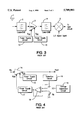
- FIG. 3 shows a block diagram of an example of the receiving front end portion of a portable mobile-communication system, for example a personal hand-phone system (PHS), of L to S bands using this type of GaAs FET amplifier.
- a received signal input from an antenna 1 passes through a band-pass filter 2 and is power-amplified by a low-noise amplifier 3.
- the amplifier 3 is the section relating to the present invention.
- the output of the amplifier 3 further passes through a band-pass filter 4 and thereafter, it is mixed with a local oscillator signal LO output from a local oscillator (not shown) by a mixer 5, converted to an intermediate-frequency signal IF, and set to the next circuit (not shown).
- a direct current (DC) gate bias voltage of the GaAs FET constituting the amplifier 3 has generally been fixed to a certain value. Therefore, a noise figure (NF) or gain characteristic of the amplifier 3 is kept at a certain value.
- NF noise figure
- levels of a received signal input from the antenna 1 of the portable system greatly change depending on the distance between a base station and the portable system or the surrounding environment. Therefore, it may be impossible to fetch information by demodulating received signals because the received signals are excessively input and mixer 5 is saturated.
- the amplifier 3 is generally designed so that the mixer 5 is not saturated even when the received-signal level is over-input by keeping the gain of the amplifier 3 at a certain level or lower.
- the amplifier 3 is designed as described above, a problem occurs that a receiving sensitivity is lowered when the received-signal level is low.
- FIG. 4 shows a block diagram of the amplifier disclosed in the Japanese Utility Model Application Laid-Open Hei 1-160709 as an example of the above type of amplifier.
- the amplifier detects an output level of a GaAs FET amplifier 14 by a detection circuit 16.
- the amplifier controls an output electric power P out of the amplifier 14 by comparing the detected level with a reference voltage by a comparison circuit (comprising an operational amplifier 18 and a voltage generation circuit 19) and changing the gate bias voltages of the GaAs FET by a D/D converter 17 in accordance with the comparison result. That is, in the case of the amplifier provided with AGC function disclosed in the above conventional art, the out electric power P out is controlled not directly by an input electric power P in of a high-frequency input signal but indirectly through a process of detecting an output level of the amplifier.
- AGC automatic gain control
- GaAs FET amplifier provided with AGC function disclosed in the above conventional art to, for example, the receiving front end of the portable mobile-communication system of L to S bands shown in FIG. 3, a plurality of peripheral units and circuits such as the detection circuit 16, offset voltage generation circuit 19, and operational amplifier 18 are necessary in order to detect an output level of the amplifier 14. Moreover, because the gate bias voltages of the GaAs FET are changed in accordance with the detected level, extra software and circuits such as a program for determining a level of the gate bias voltage and the D/D converter 17 for actually supplying the gate bias voltage in accordance with the program are necessary on the signal line.
- a coupler for detecting an output level of the amplifier (not shown) and a diode for wave detection (not shown) are necessary on the signal line. That is, problems occur in that costs are increased due to increase of the steps for managing parts and assembling, mounting area increases, and thereby, loss is produced.
- an object of the preset invention is to decrease power consumption, occupying area and costs.
- the semiconductor circuit of the present invention comprises a barrier-gate transistor connected between a first voltage line and a second voltage line, and a gate of the barrier-gate transistor being connected to a first node, and a circuit connected to the first node for controlling an amplification gain of the barrier-gate transistor in accordance with a signal power applying to the first node.
- the high-frequency amplifier of the present invention uses the fact that the gradient of a gate current-voltage characteristic curve of a barrier-gate FET serving as an amplification device is asymmetric to a certain value of the gate-source voltage (equivalent to the anode-cathode voltage of a diode) in a reverse-direction region. That is, when swinging the gate-source voltage of an FET in the positive direction and the negative direction equally about the change point of the gate current-voltage characteristic in accordance with a high-frequency input signal, reverse gate current changes because current with the largest current change rate is added to the original current as a difference.
- the direction of the change is the same as a direction for decreasing a reverse gate current (bound for a gate electrode from a channel by exceeding a gate barrier).
- the current flowing through a resistance for determining the gate voltage of an FET is decreased due to decrease of the reverse gate current.
- the effective gate bias voltage of the FET deepens in the negative direction, the drain-source current decreases, and the gain of an amplifier decreases.
- FIGS. 1(a), 1(b) are a circuit diagram of an embodiment of the present invention and an illustration showing the current-voltage characteristic of the Schottky barrier gate of a GaAs FET using the embodiment;
- FIG. 2 is an illustration showing the characteristic of the initial amplification stage of the circuit shown in Fig. 1(a);
- FIG. 3 is a block diagram of the receiving front-end section of PHS.
- FIG. 4 is a block diagram of a conventional amplifier.
- An embodiment of the high-frequency amplifier shown in FIG. 1(a) comprises a two vertical GaAs FET amplification parts.
- the first amplification part comprises an n-channel depletion-type GaAs FET Q1, a capacitor C1, a pair of resistors RG1 and RG2.
- the final amplification part comprises a GaAs FETQ 2 serving as an amplification device, a load resistance R L2 , and two serially-connected resistances R G3 and R G4 constituting a gate bias circuit.
- the FETQ 2 is also the n-channel depletion type. Each elements of the final amplification part is connected similarly to the initial amplification part.
- the gate of the GaAs FETQ2 is connected to the drain of the GaAs FETQ1 through a capacitor C2 and a micro-strip line having L component.
- the drain of the GaAs FETQ2 is connected to an output terminal Pout through a capacitor C3.
- this embodiment comprises two vertical amplification parts, the final amplification part has the same structure as the initial amplification part as shown by the circuit diagram in FIG. 1(a).
- the final amplification part is used as an output stage for adjustment of the whole amplification rate or adjustment of output impedance.
- the present invention has a double-stage structure, and the functions and advantages of the present invention can be obtained even if the present invention is an amplifier having a single-stage structure of only the initial or final amplification part. Therefore, the subsequent description is made mainly for the initial amplification part.
- FIG. 1(a) it is assumed that R G1 is equal to 2 k ⁇ , R G2 is equal to 1 k ⁇ , R G3 and R G4 are equal to 3 k ⁇ , and V GG is equal to -3.0 V!.
- a reverse gate current that is, a current from the gate electrode side toward the series-connection point between the resistances R G1 and R G2 flows through the Schottky barrier diode at the gate section of the FETQ 1 but the reverse gate current is ignored as described later.
- FIG. 1(b) shows the vertical axis at the reverse current side by enlarging it to the vertical axis at the forward current side.
- V GS -2.0 V! in the case of the reverse current. That is, the gradient in a region where a reverse gate voltage V GS has a large absolute value is gradual, but it is steep in a region where the voltage V GS has a small absolute value.
- the current flowing into the series-connection point between the resistances R G1 , and R G2 from the gate electrode decreases.
- the current I R2 is almost constantly kept at -1.0 mA!.
- the output power output to the output terminal P out increases proportionally to the input power supplied to the input terminal P in and therefore, the gain G P is constantly kept at 13 dB!.
- the gate voltage V GS of the FETQ 1 shows -2.3 V!.
- the gain G P of the amplifier of the present invention is not indirectly controlled by the output power output to the output terminal P out but it is directly controlled by the input power supplied to the input terminal P in .
- the amplification device of the present invention uses a Schottky barrier-gate (SBG) FET such as a GaAs FET.
- SBG FET Schottky barrier-gate
- MOS metal oxide semiconductor
- the present invention positively uses the fact that a reverse gate current flows. That is, by noting that the current-voltage characteristic of the reverse gate current is asymmetric to a DC bias point, a DC bias point is set to a position nearby the change point of the characteristic. To set the DC bias point, a resistance division circuit of two resistances R G1 and R G2 is used.
- the DC bias point can be determined only by the ratio between two resistance values. Moreover, a gain decrease value due to a high-frequency signal input is determined by the absolute value of a resistance.
- the bias circuit according to resistance division realizes the above mentioned.
- Resistance values of the resistances R G1 and R G2 are respectively set to the optimum value by considering the DC characteristic such as pinch-off voltage of the GaAs FETQ 1 , gate current-voltage characteristic, or withstand voltage and the AC characteristic such as frequency used, necessary output electric power output to output terminal P out , gain G P , or structure of an externally-installed circuit.
- resistance values of the gate resistances R G3 and R G4 of the rear-stage GaAs FETQ 2 are set so that they are two times or more larger than the resistance values of the resistances R G1 and R G2 respectively and the current I R4 flowing through the resistance R G4 at the final amplification stage is smaller than the current I R2 flowing through the resistance R G2 at the front amplification stage, the impedance at the output side does not fluctuate and influence on the mixer at the next stage can almost be ignored because the idle current of the final-stage FETQ 2 hardly fluctuates.
- the amplification device uses a GaAs SBG FET.
- the amplification device is not restricted to the GaAs SBG FET. It is also possible to use an FET having other structure as long as the FET is of the barrier gate type.
- an FET having a heterojunction structure obtained by joining semiconductors each other and an SBG FET made of silicon are listed. Moreover, it is possible to use an FET having a pn-junction gate structure.
- the amplifier of the present invention uses an FET having a Schottky barrier or a barrier of heterojunction or pn-junction at a gate section like a GaAs FET as the amplification device and it is constituted so as to directly control gain by input power and automatically decrease the gain for an over-input by using the fact that reverse current flowing through a gate barrier shows a behavior asymmetric to the DC bias point of a gate and thereby flowing the current through the barrier gate.
- the present invention makes it possible to decrease the gain for an over-input by a simple circuit structure, compared to a conventional amplifier which monitors output power and changes a gate voltage in accordance with the monitored result.
- the amplifier of the present invention does not require any peripheral part or program for gain control differently from a conventional amplifier. Therefore, the amplifier of the present invention is superior to the conventional amplifier in the mounting area and makes it possible to decrease the manufacturing cost including part management man-hours and assembling man-hours.
- the amplifier of the present invention using a microwave band transistor such as a GaAs FET for the amplification device is very effective when using the amplifier for the receiving front-end section of a portable mobile-communication system of L to S bands whose small size and low cost are stressed such as PHS.
Landscapes
- Engineering & Computer Science (AREA)
- Power Engineering (AREA)
- Amplifiers (AREA)
- Control Of Amplification And Gain Control (AREA)
Abstract
Description
Claims (9)
Applications Claiming Priority (2)
| Application Number | Priority Date | Filing Date | Title |
|---|---|---|---|
| JP7040170A JP2685014B2 (en) | 1995-02-28 | 1995-02-28 | High frequency amplifier |
| JP7-040170 | 1995-02-28 |
Publications (1)
| Publication Number | Publication Date |
|---|---|
| US5789983A true US5789983A (en) | 1998-08-04 |
Family
ID=12573301
Family Applications (1)
| Application Number | Title | Priority Date | Filing Date |
|---|---|---|---|
| US08/604,238 Expired - Fee Related US5789983A (en) | 1995-02-28 | 1996-02-21 | High-frequency amplifier having variable gain in response to input power level |
Country Status (2)
| Country | Link |
|---|---|
| US (1) | US5789983A (en) |
| JP (1) | JP2685014B2 (en) |
Cited By (11)
| Publication number | Priority date | Publication date | Assignee | Title |
|---|---|---|---|---|
| US6111466A (en) * | 1999-03-22 | 2000-08-29 | Motorola, Inc. | Amplifier with feedback to provide bias adjustment |
| US6239625B1 (en) * | 1998-08-20 | 2001-05-29 | Sony Corporation | Detection circuit |
| US6323731B1 (en) * | 2000-10-06 | 2001-11-27 | Tropion, Inc. Corp. | Variable bias control for switch mode RF amplifier |
| US6388526B1 (en) * | 2000-07-06 | 2002-05-14 | Lucent Technologies Inc. | Methods and apparatus for high performance reception of radio frequency communication signals |
| WO2002080357A1 (en) * | 2001-03-29 | 2002-10-10 | Gct Semiconductor, Inc. | Variable gain low-noise amplifier for a wireless terminal |
| US6735424B1 (en) * | 2000-06-14 | 2004-05-11 | The Regents Of The University Of California | S-band low-noise amplifier with self-adjusting bias for improved power consumption and dynamic range in a mobile environment |
| US20040201424A1 (en) * | 2003-04-12 | 2004-10-14 | Dow-Chih Niu | Idss RF amplifier |
| US20040207468A1 (en) * | 2002-10-17 | 2004-10-21 | Armin Klomsdorf | Power amplification circuit and method for supplying power at a plurality of desired power output levels |
| US20050083128A1 (en) * | 2003-10-16 | 2005-04-21 | Yi-Jen Chan | [power amplifier with active bias circuit] |
| US20070021087A1 (en) * | 2005-07-21 | 2007-01-25 | Microsoft Corporation | Dynamic bias for receiver controlled by radio link quality |
| RU2568264C1 (en) * | 2014-10-15 | 2015-11-20 | Акционерное общество "Научно-производственное предприятие "Исток" имени А.И. Шокина" (АО "НПП "Исток" им. Шокина") | Voltage-controlled generator |
Citations (3)
| Publication number | Priority date | Publication date | Assignee | Title |
|---|---|---|---|---|
| JPH01160709A (en) * | 1987-12-18 | 1989-06-23 | Yokohama Rubber Co Ltd:The | Pneumatic radial tire |
| US5371477A (en) * | 1991-08-05 | 1994-12-06 | Matsushita Electric Industrial Co. Ltd. | Linear amplifier |
| US5392004A (en) * | 1992-11-04 | 1995-02-21 | U.S. Philips Corporation | Combination amplifier/bias voltage generator |
Family Cites Families (2)
| Publication number | Priority date | Publication date | Assignee | Title |
|---|---|---|---|---|
| JPH02149108A (en) * | 1988-11-30 | 1990-06-07 | Nec Corp | Gate voltage control circuit |
| JPH04356805A (en) * | 1991-06-03 | 1992-12-10 | Fujitsu Ltd | Amplifier |
-
1995
- 1995-02-28 JP JP7040170A patent/JP2685014B2/en not_active Expired - Fee Related
-
1996
- 1996-02-21 US US08/604,238 patent/US5789983A/en not_active Expired - Fee Related
Patent Citations (3)
| Publication number | Priority date | Publication date | Assignee | Title |
|---|---|---|---|---|
| JPH01160709A (en) * | 1987-12-18 | 1989-06-23 | Yokohama Rubber Co Ltd:The | Pneumatic radial tire |
| US5371477A (en) * | 1991-08-05 | 1994-12-06 | Matsushita Electric Industrial Co. Ltd. | Linear amplifier |
| US5392004A (en) * | 1992-11-04 | 1995-02-21 | U.S. Philips Corporation | Combination amplifier/bias voltage generator |
Cited By (18)
| Publication number | Priority date | Publication date | Assignee | Title |
|---|---|---|---|---|
| US6239625B1 (en) * | 1998-08-20 | 2001-05-29 | Sony Corporation | Detection circuit |
| US6111466A (en) * | 1999-03-22 | 2000-08-29 | Motorola, Inc. | Amplifier with feedback to provide bias adjustment |
| USRE41582E1 (en) * | 2000-06-14 | 2010-08-24 | The Regents Of The University Of California | S-band low-noise amplifier with self-adjusting bias for improved power consumption and dynamic range in a mobile environment |
| US6735424B1 (en) * | 2000-06-14 | 2004-05-11 | The Regents Of The University Of California | S-band low-noise amplifier with self-adjusting bias for improved power consumption and dynamic range in a mobile environment |
| US6388526B1 (en) * | 2000-07-06 | 2002-05-14 | Lucent Technologies Inc. | Methods and apparatus for high performance reception of radio frequency communication signals |
| US6323731B1 (en) * | 2000-10-06 | 2001-11-27 | Tropion, Inc. Corp. | Variable bias control for switch mode RF amplifier |
| CN100409565C (en) * | 2000-10-06 | 2008-08-06 | 松下电器产业株式会社 | Variable Bias Control for Switch-Mode RF Amplifiers |
| CN1315255C (en) * | 2001-03-29 | 2007-05-09 | Gct半导体公司 | Variable gain low-noise amplifier for a wireless terminal |
| US6657498B2 (en) | 2001-03-29 | 2003-12-02 | Gct Semiconductor, Inc. | Variable gain low-noise amplifier for a wireless terminal |
| WO2002080357A1 (en) * | 2001-03-29 | 2002-10-10 | Gct Semiconductor, Inc. | Variable gain low-noise amplifier for a wireless terminal |
| US20040207468A1 (en) * | 2002-10-17 | 2004-10-21 | Armin Klomsdorf | Power amplification circuit and method for supplying power at a plurality of desired power output levels |
| US7064611B2 (en) * | 2003-04-12 | 2006-06-20 | Chung-Shan Institute Of Science And Technology | IDSS RF amplifier |
| US20040201424A1 (en) * | 2003-04-12 | 2004-10-14 | Dow-Chih Niu | Idss RF amplifier |
| US20050083128A1 (en) * | 2003-10-16 | 2005-04-21 | Yi-Jen Chan | [power amplifier with active bias circuit] |
| US7368995B2 (en) * | 2003-10-16 | 2008-05-06 | Novatek Microelectronics Corp. | Power amplifier with active bias circuit |
| US20070021087A1 (en) * | 2005-07-21 | 2007-01-25 | Microsoft Corporation | Dynamic bias for receiver controlled by radio link quality |
| US7599670B2 (en) * | 2005-07-21 | 2009-10-06 | Microsoft Corporation | Dynamic bias for receiver controlled by radio link quality |
| RU2568264C1 (en) * | 2014-10-15 | 2015-11-20 | Акционерное общество "Научно-производственное предприятие "Исток" имени А.И. Шокина" (АО "НПП "Исток" им. Шокина") | Voltage-controlled generator |
Also Published As
| Publication number | Publication date |
|---|---|
| JPH08237041A (en) | 1996-09-13 |
| JP2685014B2 (en) | 1997-12-03 |
Similar Documents
| Publication | Publication Date | Title |
|---|---|---|
| KR100302685B1 (en) | Amplifier circuit and multistage amplifier circuit | |
| US7636004B2 (en) | High-frequency switching device and semiconductor | |
| US7738845B2 (en) | Electronic parts for high frequency power amplifier and wireless communication device | |
| US6967528B2 (en) | Variable gain amplifier | |
| US5789983A (en) | High-frequency amplifier having variable gain in response to input power level | |
| US7026858B2 (en) | Switch semiconductor integrated circuit | |
| US20070216482A1 (en) | High linearity and low noise amplifier with continuously variable gain control | |
| CN110463035B (en) | Current reuse type field effect transistor amplifier | |
| US20020140502A1 (en) | RF variable gain amplifying device | |
| US6211729B1 (en) | Amplifier circuit with a switch bypass | |
| GB2334838A (en) | Variable rf attenuator using shunt connected antiparallel pair of bipolar transistors | |
| US6239659B1 (en) | Low power gain controlled amplifier with high dynamic range | |
| US10116273B2 (en) | Current reuse field effect transistor amplifier | |
| KR100780399B1 (en) | Bias Circuit and Wireless Communication Device Using the Same | |
| EP1153475B1 (en) | Gate biasing arrangement | |
| US6999740B2 (en) | Semiconductor integrated circuit and radio communication apparatus using same | |
| US6118338A (en) | Low noise amplifier circuit with an isolating switch topology | |
| KR20020008746A (en) | Variable gain amplifier | |
| US6904271B2 (en) | High-frequency-signal switching circuit suppressing high-frequency-signal distortion | |
| US7667532B1 (en) | Bias control system for a power amplifier | |
| US5670893A (en) | BiCMOS logic circuit with bipolar base clamping | |
| US20010009390A1 (en) | OW current amplifier circuit with protection against static electricity | |
| JP2000323944A (en) | High frequency gain variable amplifier | |
| US6420923B1 (en) | Low supply, current-controlled FET Pi attenuator | |
| KR0120723B1 (en) | Switch circuit for monolithic microwave integrated circuits |
Legal Events
| Date | Code | Title | Description |
|---|---|---|---|
| AS | Assignment |
Owner name: NEC CORPORATION, JAPAN Free format text: ASSIGNMENT OF ASSIGNORS INTEREST;ASSIGNOR:FUJITA, MASANORI;REEL/FRAME:007886/0615 Effective date: 19960216 |
|
| FEPP | Fee payment procedure |
Free format text: PAYOR NUMBER ASSIGNED (ORIGINAL EVENT CODE: ASPN); ENTITY STATUS OF PATENT OWNER: LARGE ENTITY |
|
| FPAY | Fee payment |
Year of fee payment: 4 |
|
| AS | Assignment |
Owner name: NEC COMPOUND SEMICONDUCTOR DEVICES, LTD., JAPAN Free format text: ASSIGNMENT OF ASSIGNORS INTEREST;ASSIGNOR:NEC CORPORATION;REEL/FRAME:013852/0613 Effective date: 20020919 |
|
| FPAY | Fee payment |
Year of fee payment: 8 |
|
| AS | Assignment |
Owner name: NEC ELECTRONICS CORPORATION, JAPAN Free format text: ASSIGNMENT OF ASSIGNORS INTEREST;ASSIGNOR:NEC COMPOUND SEMICONDUCTOR DEVICES, LTD.;REEL/FRAME:017422/0528 Effective date: 20060315 |
|
| REMI | Maintenance fee reminder mailed | ||
| LAPS | Lapse for failure to pay maintenance fees | ||
| STCH | Information on status: patent discontinuation |
Free format text: PATENT EXPIRED DUE TO NONPAYMENT OF MAINTENANCE FEES UNDER 37 CFR 1.362 |
|
| FP | Lapsed due to failure to pay maintenance fee |
Effective date: 20100804 |