US5695658A - Non-photolithographic etch mask for submicron features - Google Patents
Non-photolithographic etch mask for submicron features Download PDFInfo
- Publication number
- US5695658A US5695658A US08/614,778 US61477896A US5695658A US 5695658 A US5695658 A US 5695658A US 61477896 A US61477896 A US 61477896A US 5695658 A US5695658 A US 5695658A
- Authority
- US
- United States
- Prior art keywords
- substrate
- droplets
- pattern
- masking layer
- tips
- Prior art date
- Legal status (The legal status is an assumption and is not a legal conclusion. Google has not performed a legal analysis and makes no representation as to the accuracy of the status listed.)
- Expired - Lifetime
Links
- 239000000758 substrate Substances 0.000 claims abstract description 79
- 238000000034 method Methods 0.000 claims abstract description 67
- 239000007788 liquid Substances 0.000 claims abstract description 32
- 238000000059 patterning Methods 0.000 claims abstract description 29
- 238000005530 etching Methods 0.000 claims abstract description 20
- 230000000873 masking effect Effects 0.000 claims description 29
- 229920002120 photoresistant polymer Polymers 0.000 claims description 18
- 238000004519 manufacturing process Methods 0.000 claims description 15
- 239000000463 material Substances 0.000 claims description 10
- 238000005507 spraying Methods 0.000 claims description 3
- VYPSYNLAJGMNEJ-UHFFFAOYSA-N Silicium dioxide Chemical compound O=[Si]=O VYPSYNLAJGMNEJ-UHFFFAOYSA-N 0.000 description 10
- 239000006185 dispersion Substances 0.000 description 7
- 239000000443 aerosol Substances 0.000 description 6
- 235000012239 silicon dioxide Nutrition 0.000 description 5
- 239000000377 silicon dioxide Substances 0.000 description 5
- 239000007921 spray Substances 0.000 description 5
- VAYOSLLFUXYJDT-RDTXWAMCSA-N Lysergic acid diethylamide Chemical compound C1=CC(C=2[C@H](N(C)C[C@@H](C=2)C(=O)N(CC)CC)C2)=C3C2=CNC3=C1 VAYOSLLFUXYJDT-RDTXWAMCSA-N 0.000 description 3
- 230000015572 biosynthetic process Effects 0.000 description 3
- 238000000206 photolithography Methods 0.000 description 3
- 239000004065 semiconductor Substances 0.000 description 3
- 125000006850 spacer group Chemical group 0.000 description 3
- XUIMIQQOPSSXEZ-UHFFFAOYSA-N Silicon Chemical compound [Si] XUIMIQQOPSSXEZ-UHFFFAOYSA-N 0.000 description 2
- 238000011161 development Methods 0.000 description 2
- 239000002270 dispersing agent Substances 0.000 description 2
- 238000001035 drying Methods 0.000 description 2
- 238000005516 engineering process Methods 0.000 description 2
- 239000002086 nanomaterial Substances 0.000 description 2
- 239000002245 particle Substances 0.000 description 2
- 238000012545 processing Methods 0.000 description 2
- 229910052710 silicon Inorganic materials 0.000 description 2
- 239000010703 silicon Substances 0.000 description 2
- OAICVXFJPJFONN-UHFFFAOYSA-N Phosphorus Chemical compound [P] OAICVXFJPJFONN-UHFFFAOYSA-N 0.000 description 1
- 230000002411 adverse Effects 0.000 description 1
- 238000013459 approach Methods 0.000 description 1
- 239000011324 bead Substances 0.000 description 1
- 150000001875 compounds Chemical class 0.000 description 1
- 238000010276 construction Methods 0.000 description 1
- 238000013461 design Methods 0.000 description 1
- 238000009826 distribution Methods 0.000 description 1
- 230000000694 effects Effects 0.000 description 1
- 230000005684 electric field Effects 0.000 description 1
- 230000008030 elimination Effects 0.000 description 1
- 238000003379 elimination reaction Methods 0.000 description 1
- 238000001704 evaporation Methods 0.000 description 1
- 230000008020 evaporation Effects 0.000 description 1
- 238000011065 in-situ storage Methods 0.000 description 1
- 239000012212 insulator Substances 0.000 description 1
- 238000001459 lithography Methods 0.000 description 1
- 239000002184 metal Substances 0.000 description 1
- 239000003595 mist Substances 0.000 description 1
- 239000000203 mixture Substances 0.000 description 1
- 229910021421 monocrystalline silicon Inorganic materials 0.000 description 1
- 230000003647 oxidation Effects 0.000 description 1
- 238000007254 oxidation reaction Methods 0.000 description 1
- 230000002093 peripheral effect Effects 0.000 description 1
- 230000010363 phase shift Effects 0.000 description 1
- 239000002243 precursor Substances 0.000 description 1
- 230000035945 sensitivity Effects 0.000 description 1
- 239000007787 solid Substances 0.000 description 1
- 238000009987 spinning Methods 0.000 description 1
- 239000000725 suspension Substances 0.000 description 1
- 238000009827 uniform distribution Methods 0.000 description 1
- 238000001429 visible spectrum Methods 0.000 description 1
Images


Classifications
-
- G—PHYSICS
- G03—PHOTOGRAPHY; CINEMATOGRAPHY; ANALOGOUS TECHNIQUES USING WAVES OTHER THAN OPTICAL WAVES; ELECTROGRAPHY; HOLOGRAPHY
- G03F—PHOTOMECHANICAL PRODUCTION OF TEXTURED OR PATTERNED SURFACES, e.g. FOR PRINTING, FOR PROCESSING OF SEMICONDUCTOR DEVICES; MATERIALS THEREFOR; ORIGINALS THEREFOR; APPARATUS SPECIALLY ADAPTED THEREFOR
- G03F7/00—Photomechanical, e.g. photolithographic, production of textured or patterned surfaces, e.g. printing surfaces; Materials therefor, e.g. comprising photoresists; Apparatus specially adapted therefor
- G03F7/16—Coating processes; Apparatus therefor
- G03F7/164—Coating processes; Apparatus therefor using electric, electrostatic or magnetic means; powder coating
-
- H—ELECTRICITY
- H01—ELECTRIC ELEMENTS
- H01J—ELECTRIC DISCHARGE TUBES OR DISCHARGE LAMPS
- H01J9/00—Apparatus or processes specially adapted for the manufacture, installation, removal, maintenance of electric discharge tubes, discharge lamps, or parts thereof; Recovery of material from discharge tubes or lamps
- H01J9/02—Manufacture of electrodes or electrode systems
- H01J9/022—Manufacture of electrodes or electrode systems of cold cathodes
- H01J9/025—Manufacture of electrodes or electrode systems of cold cathodes of field emission cathodes
-
- H—ELECTRICITY
- H01—ELECTRIC ELEMENTS
- H01L—SEMICONDUCTOR DEVICES NOT COVERED BY CLASS H10
- H01L21/00—Processes or apparatus adapted for the manufacture or treatment of semiconductor or solid state devices or of parts thereof
- H01L21/02—Manufacture or treatment of semiconductor devices or of parts thereof
- H01L21/04—Manufacture or treatment of semiconductor devices or of parts thereof the devices having potential barriers, e.g. a PN junction, depletion layer or carrier concentration layer
- H01L21/18—Manufacture or treatment of semiconductor devices or of parts thereof the devices having potential barriers, e.g. a PN junction, depletion layer or carrier concentration layer the devices having semiconductor bodies comprising elements of Group IV of the Periodic Table or AIIIBV compounds with or without impurities, e.g. doping materials
- H01L21/30—Treatment of semiconductor bodies using processes or apparatus not provided for in groups H01L21/20 - H01L21/26
- H01L21/302—Treatment of semiconductor bodies using processes or apparatus not provided for in groups H01L21/20 - H01L21/26 to change their surface-physical characteristics or shape, e.g. etching, polishing, cutting
- H01L21/306—Chemical or electrical treatment, e.g. electrolytic etching
- H01L21/308—Chemical or electrical treatment, e.g. electrolytic etching using masks
- H01L21/3081—Chemical or electrical treatment, e.g. electrolytic etching using masks characterised by their composition, e.g. multilayer masks, materials
-
- H—ELECTRICITY
- H01—ELECTRIC ELEMENTS
- H01L—SEMICONDUCTOR DEVICES NOT COVERED BY CLASS H10
- H01L21/00—Processes or apparatus adapted for the manufacture or treatment of semiconductor or solid state devices or of parts thereof
- H01L21/02—Manufacture or treatment of semiconductor devices or of parts thereof
- H01L21/04—Manufacture or treatment of semiconductor devices or of parts thereof the devices having potential barriers, e.g. a PN junction, depletion layer or carrier concentration layer
- H01L21/18—Manufacture or treatment of semiconductor devices or of parts thereof the devices having potential barriers, e.g. a PN junction, depletion layer or carrier concentration layer the devices having semiconductor bodies comprising elements of Group IV of the Periodic Table or AIIIBV compounds with or without impurities, e.g. doping materials
- H01L21/30—Treatment of semiconductor bodies using processes or apparatus not provided for in groups H01L21/20 - H01L21/26
- H01L21/302—Treatment of semiconductor bodies using processes or apparatus not provided for in groups H01L21/20 - H01L21/26 to change their surface-physical characteristics or shape, e.g. etching, polishing, cutting
- H01L21/306—Chemical or electrical treatment, e.g. electrolytic etching
- H01L21/308—Chemical or electrical treatment, e.g. electrolytic etching using masks
- H01L21/3083—Chemical or electrical treatment, e.g. electrolytic etching using masks characterised by their size, orientation, disposition, behaviour, shape, in horizontal or vertical plane
- H01L21/3086—Chemical or electrical treatment, e.g. electrolytic etching using masks characterised by their size, orientation, disposition, behaviour, shape, in horizontal or vertical plane characterised by the process involved to create the mask, e.g. lift-off masks, sidewalls, or to modify the mask, e.g. pre-treatment, post-treatment
-
- H—ELECTRICITY
- H01—ELECTRIC ELEMENTS
- H01L—SEMICONDUCTOR DEVICES NOT COVERED BY CLASS H10
- H01L21/00—Processes or apparatus adapted for the manufacture or treatment of semiconductor or solid state devices or of parts thereof
- H01L21/02—Manufacture or treatment of semiconductor devices or of parts thereof
- H01L21/04—Manufacture or treatment of semiconductor devices or of parts thereof the devices having potential barriers, e.g. a PN junction, depletion layer or carrier concentration layer
- H01L21/18—Manufacture or treatment of semiconductor devices or of parts thereof the devices having potential barriers, e.g. a PN junction, depletion layer or carrier concentration layer the devices having semiconductor bodies comprising elements of Group IV of the Periodic Table or AIIIBV compounds with or without impurities, e.g. doping materials
- H01L21/30—Treatment of semiconductor bodies using processes or apparatus not provided for in groups H01L21/20 - H01L21/26
- H01L21/31—Treatment of semiconductor bodies using processes or apparatus not provided for in groups H01L21/20 - H01L21/26 to form insulating layers thereon, e.g. for masking or by using photolithographic techniques; After treatment of these layers; Selection of materials for these layers
- H01L21/3105—After-treatment
- H01L21/311—Etching the insulating layers by chemical or physical means
- H01L21/31144—Etching the insulating layers by chemical or physical means using masks
-
- H—ELECTRICITY
- H01—ELECTRIC ELEMENTS
- H01L—SEMICONDUCTOR DEVICES NOT COVERED BY CLASS H10
- H01L21/00—Processes or apparatus adapted for the manufacture or treatment of semiconductor or solid state devices or of parts thereof
- H01L21/02—Manufacture or treatment of semiconductor devices or of parts thereof
- H01L21/04—Manufacture or treatment of semiconductor devices or of parts thereof the devices having potential barriers, e.g. a PN junction, depletion layer or carrier concentration layer
- H01L21/18—Manufacture or treatment of semiconductor devices or of parts thereof the devices having potential barriers, e.g. a PN junction, depletion layer or carrier concentration layer the devices having semiconductor bodies comprising elements of Group IV of the Periodic Table or AIIIBV compounds with or without impurities, e.g. doping materials
- H01L21/30—Treatment of semiconductor bodies using processes or apparatus not provided for in groups H01L21/20 - H01L21/26
- H01L21/31—Treatment of semiconductor bodies using processes or apparatus not provided for in groups H01L21/20 - H01L21/26 to form insulating layers thereon, e.g. for masking or by using photolithographic techniques; After treatment of these layers; Selection of materials for these layers
- H01L21/3205—Deposition of non-insulating-, e.g. conductive- or resistive-, layers on insulating layers; After-treatment of these layers
- H01L21/321—After treatment
- H01L21/3213—Physical or chemical etching of the layers, e.g. to produce a patterned layer from a pre-deposited extensive layer
- H01L21/32139—Physical or chemical etching of the layers, e.g. to produce a patterned layer from a pre-deposited extensive layer using masks
Definitions
- the apparatus comprises the reservoir area 9A, the trajectory area 9B, and substrate unit 9C.
- the reservoir area 9A comprises a nozzle 8 which contains a capillary tube 8 into which is dispensed the photoresist 2A and a metal electrode 8B.
- the electrode 8A functions to impart a charge onto the liquid 2A at the end of the capillary tube 8.
- the electrode functions as cathode when charged by the voltage source 20.
Landscapes
- Engineering & Computer Science (AREA)
- Physics & Mathematics (AREA)
- General Physics & Mathematics (AREA)
- Manufacturing & Machinery (AREA)
- Condensed Matter Physics & Semiconductors (AREA)
- Computer Hardware Design (AREA)
- Microelectronics & Electronic Packaging (AREA)
- Power Engineering (AREA)
- ing And Chemical Polishing (AREA)
- Cold Cathode And The Manufacture (AREA)
Abstract
A non-photolithographic, physical patterning process, which is useful for selectively etching of a substrate, is provided. The process comprises electrostatically charging liquid droplets which are selectively etchable with respect to the substrate, dispersing the droplets onto substrate in a pattern; and etching the substrate using the droplets as a mask.
Description
This invention relates to masking and patterning technology, and more particularly to liquid dispersions for use as non-photolithographic etch masks for submicron features.
In the semiconductor industry, patterning is typically accomplished by spinning a film of photoresist material onto a wafer. The photoresist is then patterned using a reticle through which light is directed. The exposed portions of the photoresist are developed and the undesired portions are washed away.
However, photolithography using the visible spectrum of light is reaching its manufacturing limits. The 0.25μ feature geometries will require new and aggressive techniques for patterning and masking steps. Currently, there is a great deal of effort being expended to make use of wavelengths in the deep ultra-violet range, as well as the use of x-rays. Phase-shift masks are also being considered as an option for use in photolithography steps.
The development of flat panel displays is also spurring the development of robust patterning processes that can be repeated over large areas in the manufacture of pixels and other features. For example, evacuated displays necessitate spacer structures strong enough to prevent implosion, but patterned small enough to go unnoticed by the human eye. Field emitter displays, in particular, contain multitudes of micro-machined cold cathode emitters which also must be patterned.
Manufacturing environments require processes that produce substantially uniform and stable results. In the manufacture of an array of emitter tips, the tips should be of uniform height, aspect ratio, sharpness, and general shape, with minimum deviation, particularly in the uppermost portion. The inherent sensitivities of and variations in photo patterning reliability compound the problems of etch uniformity.
Fabrication of a uniform array of cathode emitter tips is very difficult to accomplish in a manufacturing environment for a number of reasons. Generally, it is difficult to attain plasma tip etches with uniformities better than 5%. Uniformities of 10%-20% are more commonly achieved. In addition, ,the oxidation necessary to "sharpen" or point the tip can vary by as much as 20%, thereby increasing the possibility of non-uniformity among the numerous tips in the array. Hence, a highly uniform patterning method is needed to minimize the effects of other process non-uniformities.
The present, invention provides the manufacturer with the ability to more directly control or write a pattern of photoresist, thereby eliminating the need for a photolithographic patterning step. The elimination of a photolithographic step is always advantageous, since photo patterning steps are often very expensive, and detract from the robustness of a process due to the limitations imposed by the usable wavelengths of light.
The process of the present invention can be used to pattern submicron features, such as field emitter tips using a single step (in situ) or multi-step plasma dry etch process. The mask layer is formed such that it exposes the silicon substrate, which silicon substrate is then etched to form the semiconductor feature or field emitter tips.
One advantage of the process of the present invention is that it enables the fabrication of emitter tips having more uniform distribution of tip dimensions. Another advantage is that it enables the formation of a good distribution of extremely sharp points which may be enhanced by further processing, but are enabled functional with etching as a tip formation only. Yet still another advantage is that it can be used with the overetching methods. See, for example, U.S. Pat. No. 5,391,259 entitled "A Method for Forming a Substantially Uniform Array of Sharp Tips."
One aspect of the process of the present invention involves a non-photlithographic, physical patterning process, useful for selectively etching of a substrate. The process comprises electrostatically charging liquid droplets which are selectively etchable with respect to the substrate, dispersing droplets onto substrate in a pattern; and etching the substrate using the droplets as a mask.
Another aspect of the process of the present invention involves a masking process useful in submicron features. An oxide layer is formed superjacent a substrate. The oxide layer is patterned using photoresist droplets, and then the oxide layer is etched.
Yet another aspect of the process of the present invention involves a patterning process useful for fabricating micro-tips. A first layer is formed superjacent a substrate, and a layer of droplets or micro-drops is placed upon the first layer. The first layer is etched, and the substrate is also etched, thereby fabricating micro-tips.
The present invention will be better understood from reading the following description of nonlimitative embodiments, with reference to the attached drawings, wherein below:
FIG. 1A is a schematic cross-section of a representative atomizer-type dispenser spraying droplets on an etchable substrate, according a first embodiment of the process of the present invention;
FIG. 1B is a schematic cross-section of the dispenser of FIG. 1A, additionally comprising a shadowmask, according to a second embodiment of the process of the present invention;
FIG. 2 is a top-view of a photolithographic mask disposed over an array of patterning droplets, according to a third embodiment of the process of the present invention;
FIG. 3 is a top-view of the array of patterning droplets of FIG. 2, after exposure, according to the process of the present invention;
FIG. 4 is a top-view of a substrate onto which droplets are dispensed in a rastering fashion, according to the process of the present invention;
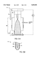
FIGS. 5A and 5B are schematic cross-sections of capillary needles used to charge liquid cluster beams, useful in the process of the present invention;
FIG. 6 is a schematic cross-section of a representative field emission display having micro-tips formed according to the process of the present invention,
FIG. 7 is a schematic cross-section of a layered substrate having droplets disposed thereon, according to the process of the present invention;
FIG. 8 is a schematic cross-section of the layered substrate of FIG. 7, after the masking layer has been etched, according to the process of the present invention;
FIG. 9 is a schematic cross-section of the layered substrate of FIG. 8, after an isotropic etch, according to the process of the present invention;
FIG. 10 is a schematic cross-section of the layered substrate of FIG. 8, after the droplets have been removed, according to an alternative embodiment of the present invention;
FIG. 11 is a schematic cross-section of the layered substrates of FIGS. 9 and 10, after the masking layer has been removed, according to the process of the present invention.
The process of the present invention is a non-photolithographic, physical approach to patterning a mask layer. It enables the formation of mask dots or circles having diameters in the range of 1 micron (μm) or less for use in critical layer lithography. The droplets (also referred to herein as dots, micro-dots, and particles) themselves, can act as the mask, so ho further patterning is needed. Hence, the process of the present invention is a physical, rather than photolithographic, masking process.
In one embodiment of the present invention, as shown in FIG. 1, the droplets 2 are preferably generated in the form of an atomized spray 2, and are therefore in liquid form. The dispersion can include, but is not limited to spray streams, jet streams, and other pressure dispersion methods. Liquid dispersants 2 are preferred, but other suspensions containing solids are also contemplated for use in the process of the present invention.
The droplets 2 can be dried during dispersion, thereby forming hardened mask beads having uniform dimensions. The drying results from the ambient into which the liquid droplets 2 are sprayed. Parameters, such as substrate temperature, ambient temperature, evaporation rate of the liquid, and viscosity of the dispersant, affect the drying rate of the droplets 2.
The dispensed droplets 2 are preferably comprised of a photoresist material, either positive or negative. However, the material used for the droplet 2 need only be selectively etchable with respect to the underlying substrate 3, 4, or 5.
For discussion purposes, a multi-layered substrate 5 comprised of at least a mask layer 3 and another layer 4 is shown. However, a single layered substrate 5 is also contemplated within the process of the present invention, for example, layer 3 or layer 4, as long as that layer 3 or 4 is selectively etchable with respect to the droplets 2 dispensed thereon.
The droplets 2, pattern the etch mask 3 or alternatively, function as the etch mask, in subsequent etching steps. Hence, the pattern or etch masks 3 formed by the droplets, and therefore the etched underlying structures, will have essentially the same size.
TSI Incorporated of St. Paul, Minn. manufactures several atomizers and aerosol generators useful in the process of the present invention. For example, the Model 3940 Submicrometer Monodisperse Aerosol Generation System can generate drops in a highly monodisperse aerosol in sizes of approximately 0.0005μ to about 1.0μ. Additionally, the Electrostatic Classifier, Model 3071A can be used for close control of drop size and dispersion. Vibrating Orifice Aerosol Generator, Model 10352 can also be used to produce droplets.
The spray stream 2 can be directed to those portions of the substrate for which masking is desired. Since the trajectory of the dispersion of the present droplets 2 used in the present invention are controllable, a relatively consistent mean (average) spacing from one droplet to the next is possible. "Overlaps," in which multiple droplets coalesce should occur at a statistically insignificant rate, if the spray stream 2 is properly adjusted.
Both aerosol and other dispersion sprays 2 are useful for this purpose. Since, each droplet 2 serves the role of an individual etch mask, and each droplet has by nature, a uniform circular cross-section, and is uniformly spaced from the other droplets, an essentially uniform array of micro-structures can be etched With manufacturing reliablilty. See, for example, FIGS. 5-9.
In another alternative embodiment of the present invention, droplets 2 of positive resist are randomly sprayed over the entire surface of the substrate 4, as shown in FIGS. 1A, 2, and 3. Subsequently, a large geometry (i.e., critical dimensions being greater than 1 μm.) masking step 6 is undertaken to develop and remove the droplets 2 from the desired locations. The remaining droplets 2 are then used as an etch mask. Similarly, negative resist can be used.
In the above-described embodiment, a photolithography step is undertaken, but the pattern does not have the same fine geometries which would be required for patterning the droplets 2. The large geometry mask 6 has dimensions that do not push the limits of technology, and is used to expose large areas of the substrate 4 at once. See, for example, FIGS. 2-3, in which the large peripheral and inter-array areas are masked 6.
Likewise, the droplets 2 can also be sprayed through a shadowmask 7, as shown in FIG. 1B. This achieves a similar result as the large geometry mask 6 described above, without the use of a lithographic step. The shadowmask 7 is aligned to the substrate 5, and the photoresist droplets 2 are thereby physically prevented from landing on the substrate 5 in the covered areas.
Another embodiment of the process of the present invention comprises the use of a charged liquid cluster beam 2A of photoresist as an etch mask. The charged liquid particles of photoresist 2A are sprayed in a substantially uniform mist over the surface of the wafer or other substrate 5, or directed to "write" a pattern thereon. By moving the dispenser nozzle 8 in relationship to the substrate, the pattern of droplets 2A can be written on the substrate 5, in a raster-like fashion, as shown in FIG. 4.
Using a charged liquid cluster beam, a single droplet 2A at a time can be dispensed upon the substrate 5, adding even greater control to the type of pattern.
FIGS. 5A and 5B, depict an apparatus capable of generating a charged liquid cluster beam. The surface of the photoresist 2A is charged so that the electrical tension force at a particular site is greater than the overall surface tension. At this point, the liquid at the site is expelled from the reservoir 9A through the capillary nozzle 8.
The apparatus comprises the reservoir area 9A, the trajectory area 9B, and substrate unit 9C. The reservoir area 9A comprises a nozzle 8 which contains a capillary tube 8 into which is dispensed the photoresist 2A and a metal electrode 8B. The electrode 8A functions to impart a charge onto the liquid 2A at the end of the capillary tube 8. The electrode functions as cathode when charged by the voltage source 20.
The trajectory area 9B is that portion of the apparatus where the stream of charged droplets 2A is directed electromagnetically (e.g., using magnets on the chamber) or heated (e.g., by inputting a heated gas into the chamber).
The substrate unit 9C is the location where the substrate 5 or wafer is mounted. The substrate unit 9C may be charged with a voltage, or alternatively heated, thereby attracting the charged droplets 2A to the surface thereof.
See, for example, "Generation of Charged Liquid Cluster Beam of Liquid-Mix Precursors and Application to Nanostructured Materials," Nanostructured Materials, Vol. 4, No. 5, pp597-602, 1994 by K. Kim and C. K. Ryu, in which this apparatus is more fully described. This reference is incorporated herein by reference to demonstrate the state of the art.
Since the expelled liquid 2A contains an electrostatic charge, its trajectory can be directed or "written." In this manner, a pattern can be imparted to a substrate 5. Portions of the substrate 5 can also be electrostatically charged with a voltage opposite that of the charged droplets 2A. In this way, path of the droplets is directed toward specific areas of the substrate 5.
For illustrative purposes, the process of the present invention is described with reference to field emission displays (FED), shown in FIG. 6. The patterning and masking aspects of the process of the present invention are well-suited for the fabrication of the very sharp cathode emitter tips 13 used in such devices.
FIG. 6 depicts the array of tips 13 in an illustrative field emission display device. At a field emission site, a micro-cathode 13 has been constructed on top of the substrate 11. Surrounding the micro-cathode 13, is a grid structure 15. When a voltage differential, through source 20, is applied between the cathode 13 and the grid 15, a stream of electrons 17 is emitted toward a phosphor coated anode screen 16.
In the preferred embodiment, the electron emission tip 13 is integral with substrate 11, and serves as a cathode. Alternatively, tip 13 can be disposed on a variety of layered and non-layered substrates and materials. Gate 15 serves as a grid structure for applying an electrical field potential to its respective cathode 13. A dielectric insulating layer 14 is deposited on the conductive cathode 13. The insulator 14 also has an opening at the field emission site location.
Disposed between said faceplate 16 and said baseplate 21 are located spacer support structures 18 which function to support the atmospheric pressure which exists on the electrode faceplate 16 as a result of the vacuum which is created between the baseplate 21 and faceplate 16 for the proper functioning of the emitter tips 13.
In the etching of cathode tips 13, it is particularly important to have uniform circular etch masks 12. The clarity, or resolution, of a field emission display is a function of a number of factors, including emitter tip 13 sharpness and uniformity of the tip array.
In the preferred embodiment of the present invention, a substrate 11 of 14-21 ohms-cms P-type 1-0-0 single crystal silicon is the material from which the tips 13 are formed, although other etchable substrates can be used. The mask 12, in the preferred embodiment, has a circular shape, and is comprised of 0.1 μm thick thermal silicon dioxide with a diameter of 1 μm.
In this example, the photoresist droplet 10 is used to pattern the silicon dioxide layer 12, which layer 12 will ultimately function as the hard etch mask 12 during the tip etching step. The photoresist droplets 10 are preferably removed after the pattern has been transferred to the silicon dioxide layer 12 via an etch step. See, for example, FIGS. 6, 7, and 9.
Alternatively, the photoresist dots 10 or droplets can remain on the silicon dioxide mask 12, during the tip etch. The mask pads 12 are etched away. When the mask pads 12 become very small or are eliminated, the micro-dots 10 are dislodged from their respective positions. When the masks 12 have been cleared, the etchant, micro-dots 10, and material from the masks 12 are removed from the etch chamber. FIG. 10 depicts the substantially uniform array of emitter tips 13 formed by the process of the present invention.
Once the patterning step has been accomplished, according to the process of the present invention, the tips structures 13 are etched. One method is taught in U.S. Pat. No. 5,391,259, in which the silicon dioxide mask 12 will adhere to the emitter tip 13 and can be overetched, beyond full undercut, without adversely effecting tip 13 shape and uniformities.
In the preferred embodiment, a dry etch to form the tip 4a proceeds for about 2.3 minutes to undercut the mask 12 and form a sharp tip 13. The tip 13 is etched vertically, as well as horizontally, and the shapes are most uniform in appearance when the rate of horizontal etching is within a factor of four to the vertical, with the most uniform results occurring after a 2:1 ratio of vertical to horizontal etching rate.
While the particular process as herein shown and disclosed in detail is fully capable of obtaining the objects and advantages herein before stated, it is to be understood that it is merely illustrative of the presently preferred embodiments of the invention and that no limitations are intended to the details of construction or design herein shown other than as described in the appended claims.
For example, one having ordinary skill in the art of etch masks will realize that the process of the present invention is equally useful for patterning spacer structures used in flat panel displays. Additionally, the process of the present invention is contemplated for patterning other submicron features used in semiconductor or other processing which requires a substantially uniform array of circular masks.
Claims (19)
1. A physical patterning process, useful for selectively etching of a substrate, said process comprising:
electrostatically charging non-colloidal liquid droplets, said droplets being selectively etchable with respect to said substrate;
dispersing said charged non-colloidal liquid droplets onto said substrate in a pattern; and
etching said substrate using said charged non-colloidal liquid droplets as a mask.
2. The physical patterning process, according to claim 1, wherein said liquid droplets comprise photoresist.
3. The physical patterning process, according to claim 2, wherein said substrate has an electrical charge, said electrical charge being opposite of said electrostatic charge on said liquid droplets.
4. A physical patterning process, useful for selectively etching of a substrate, said process comprising:
electrostatically charging liquid droplets, said droplets being selectively etchable with respect to said substrate, wherein said substrate has an electrical charge, said electrical charge being opposite of said electrostatic charge on said liquid droplets;
dispersing said charged liquid droplets onto said substrate in a pattern;
etching said substrate using said charged liquid droplets as a mask, wherein said liquid droplets comprise photoresist; and
wherein said droplets are dispersed one at a time.
5. The physical patterning process, according to claim 4, wherein said liquid droplets are dispersed in a raster-like fashion onto said substrate.
6. The physical patterning process, according to claim 5, wherein said pattern comprises an array.
7. A method of masking a substrate, said method comprising:
spraying non-particulate droplets onto said substrate, thereby patterning said substrate, each of said non-particulate droplets being substantially circular and having the same approximate diameter; and
selectively etching portions of said substrate unpatterned by said non-particulate droplets.
8. The method of masking a substrate, according to claim 7, wherein said diameter of said droplets is less than 1 μm.
9. The method of masking a substrate, according to claim 8, wherein said substrate is a multi-layered substrate, said portions of said substrate comprising a hard mask material.
10. The method of masking a substrate, according to claim 9, further comprising:
removing said droplets from said hard mask material after said portions of said substrate have been etched; and
etching said substrate through said hard mask material.
11. The method of masking a substrate, according to claim 7, wherein said droplets are sprayed through a shadow mask.
12. A method of forming an array of micro-tips, useful in field emission displays, said method comprising:
providing a substrate having a masking layer disposed thereon;
dispensing droplets onto said masking layer, thereby defining a pattern on said masking layer;
selectively removing portions of said masking layer, to transfer said pattern into said masking layer; and
isotropically etching said substrate unpatterned by said masking layer, thereby forming said micro-tips.
13. The method of making micro-tips, useful in field emission displays, according to claim 12, furhter comprising:
removing said droplets from said masking layer.
14. The method of making micro-tips, useful in field emission displays, according to claim 13, wherein said pattern is a random pattern.
15. The method of making micro-tips, useful in field emission displays, said method comprising:
providing a substrate having a masking layer disposed thereon;
dispensing droplets onto said masking layer, thereby defining a pattern on said masking layer, said pattern being a random pattern;
selectively removing portions of said masking layer, to transfer said pattern into said masking layer;
isotropically etching said substrate unpatterned by said masking layer, thereby forming said micro-tips; and
removing said droplets from said masking layer
exposing said substrate to light energy through a reticle having critical dimensions greater than 1 μm, thereby further patterning said substrate.
16. The method of making micro-tips, useful in field emission displays, according to claim 14, wherein said droplets are dispensed through a shadowmask.
17. The method of making micro-tips, useful in field emission displays, according to claim 12, wherein said droplets are substantially uniformly spaced from one another.
18. The method of making micro-tips, useful in field emission displays, according to claim 17, wherein said droplets comprise a liquid component.
19. A physical patterning process, useful for selectively etching of a substrate, said process comprising:
electrostatically charging liquid droplets, said droplets being selectively etchable with respect to said substrate;
dispersing said charged liquid droplets onto said substrate in a pattern, wherein said droplets are dispersed one at a time; and
etching said substrate using said charged liquid droplets as a mask.
Priority Applications (2)
| Application Number | Priority Date | Filing Date | Title |
|---|---|---|---|
| US08/614,778 US5695658A (en) | 1996-03-07 | 1996-03-07 | Non-photolithographic etch mask for submicron features |
| US08/900,368 US5811020A (en) | 1996-03-07 | 1997-07-23 | Non-photolithographic etch mask for submicron features |
Applications Claiming Priority (1)
| Application Number | Priority Date | Filing Date | Title |
|---|---|---|---|
| US08/614,778 US5695658A (en) | 1996-03-07 | 1996-03-07 | Non-photolithographic etch mask for submicron features |
Related Child Applications (1)
| Application Number | Title | Priority Date | Filing Date |
|---|---|---|---|
| US08/900,368 Continuation US5811020A (en) | 1996-03-07 | 1997-07-23 | Non-photolithographic etch mask for submicron features |
Publications (1)
| Publication Number | Publication Date |
|---|---|
| US5695658A true US5695658A (en) | 1997-12-09 |
Family
ID=24462656
Family Applications (2)
| Application Number | Title | Priority Date | Filing Date |
|---|---|---|---|
| US08/614,778 Expired - Lifetime US5695658A (en) | 1996-03-07 | 1996-03-07 | Non-photolithographic etch mask for submicron features |
| US08/900,368 Expired - Lifetime US5811020A (en) | 1996-03-07 | 1997-07-23 | Non-photolithographic etch mask for submicron features |
Family Applications After (1)
| Application Number | Title | Priority Date | Filing Date |
|---|---|---|---|
| US08/900,368 Expired - Lifetime US5811020A (en) | 1996-03-07 | 1997-07-23 | Non-photolithographic etch mask for submicron features |
Country Status (1)
| Country | Link |
|---|---|
| US (2) | US5695658A (en) |
Cited By (21)
| Publication number | Priority date | Publication date | Assignee | Title |
|---|---|---|---|---|
| US5871870A (en) * | 1996-05-21 | 1999-02-16 | Micron Technology, Inc. | Mask for forming features on a semiconductor substrate and a method for forming the mask |
| US6054395A (en) * | 1997-10-24 | 2000-04-25 | Micron Technology, Inc. | Method of patterning a semiconductor device |
| US6064145A (en) * | 1999-06-04 | 2000-05-16 | Winbond Electronics Corporation | Fabrication of field emitting tips |
| WO2000030767A1 (en) * | 1998-11-23 | 2000-06-02 | Applied Materials, Inc. | A photoresist coater |
| US6083767A (en) * | 1998-05-26 | 2000-07-04 | Micron Technology, Inc. | Method of patterning a semiconductor device |
| US6117791A (en) * | 1998-06-22 | 2000-09-12 | Micron Technology, Inc. | Etchant with selectivity for doped silicon dioxide over undoped silicon dioxide and silicon nitride, processes which employ the etchant, and structures formed thereby |
| US6143580A (en) * | 1999-02-17 | 2000-11-07 | Micron Technology, Inc. | Methods of forming a mask pattern and methods of forming a field emitter tip mask |
| US6174449B1 (en) | 1998-05-14 | 2001-01-16 | Micron Technology, Inc. | Magnetically patterned etch mask |
| US6228538B1 (en) * | 1998-08-28 | 2001-05-08 | Micron Technology, Inc. | Mask forming methods and field emission display emitter mask forming methods |
| US20020018172A1 (en) * | 2000-02-10 | 2002-02-14 | Alwan James J. | Method for manufacturing a flat panel display using localized wet etching |
| US6350388B1 (en) | 1999-08-19 | 2002-02-26 | Micron Technology, Inc. | Method for patterning high density field emitter tips |
| US20020113536A1 (en) * | 1999-03-01 | 2002-08-22 | Ammar Derraa | Field emitter display (FED) assemblies and methods of forming field emitter display (FED) assemblies |
| US20030027082A1 (en) * | 2001-04-19 | 2003-02-06 | Xerox Corporation | Method for printing etch masks using phase-change materials |
| US20040002225A1 (en) * | 2002-06-27 | 2004-01-01 | Xerox Corporation | Method for fabricating fine features by jet-printing and surface treatment |
| US6875371B1 (en) | 1998-06-22 | 2005-04-05 | Micron Technology, Inc. | Etchant with selectivity for doped silicon dioxide over undoped silicon dioxide and silicon nitride, processes which employ the etchant, and structures formed thereby |
| US20060202392A1 (en) * | 2005-03-14 | 2006-09-14 | Agency For Science, Technology And Research | Tunable mask apparatus and process |
| US7173339B1 (en) | 1998-06-22 | 2007-02-06 | Micron Technology, Inc. | Semiconductor device having a substrate an undoped silicon oxide structure and an overlaying doped silicon oxide structure with a sidewall terminating at the undoped silicon oxide structure |
| US20080083917A1 (en) * | 2006-10-10 | 2008-04-10 | Palo Alto Research Center Incorporated | Self-aligned masks using multi-temperature phase-change materials |
| US20080242057A1 (en) * | 2005-08-18 | 2008-10-02 | Infineon Technologies Ag | Semiconductor device with a thinned semiconductor chip and method for producing the thinned semiconductor chip |
| US20140220773A1 (en) * | 2013-02-01 | 2014-08-07 | William Marsh Rice University | Fabrication of graphene nanoribbons and nanowires |
| CN110133094A (en) * | 2019-05-14 | 2019-08-16 | 上海华虹宏力半导体制造有限公司 | The detection method of testing piece and its manufacturing method and resistdefects |
Families Citing this family (14)
| Publication number | Priority date | Publication date | Assignee | Title |
|---|---|---|---|---|
| US5796111A (en) * | 1995-10-30 | 1998-08-18 | Phrasor Scientific, Inc. | Apparatus for cleaning contaminated surfaces using energetic cluster beams |
| JP3019041B2 (en) * | 1997-09-26 | 2000-03-13 | 日本電気株式会社 | Field emission cathode and method of manufacturing the same |
| US6426233B1 (en) * | 1999-08-03 | 2002-07-30 | Micron Technology, Inc. | Uniform emitter array for display devices, etch mask for the same, and methods for making the same |
| TW495809B (en) * | 2000-02-28 | 2002-07-21 | Semiconductor Energy Lab | Thin film forming device, thin film forming method, and self-light emitting device |
| TW495812B (en) * | 2000-03-06 | 2002-07-21 | Semiconductor Energy Lab | Thin film forming device, method of forming a thin film, and self-light-emitting device |
| US6746539B2 (en) * | 2001-01-30 | 2004-06-08 | Msp Corporation | Scanning deposition head for depositing particles on a wafer |
| US6858464B2 (en) | 2002-06-19 | 2005-02-22 | Semiconductor Energy Laboratory Co., Ltd. | Method of manufacturing light emitting device |
| TWI276366B (en) * | 2002-07-09 | 2007-03-11 | Semiconductor Energy Lab | Production apparatus and method of producing a light-emitting device by using the same apparatus |
| CN101694871B (en) * | 2002-11-11 | 2012-12-05 | 株式会社半导体能源研究所 | Process for fabricating light emitting device |
| BRPI0409772A (en) * | 2003-04-28 | 2006-05-30 | Koninkl Philips Electronics Nv | method for fabricating a field emitting electrode, field emitting electrode, field emitting display device, and field emitting light source |
| CN100481406C (en) * | 2004-06-04 | 2009-04-22 | Nxp股份有限公司 | Improved etch method |
| EP1957207A1 (en) * | 2005-11-11 | 2008-08-20 | Hitachi Chemical Research Center, Inc. | Method of enhancing biocompatibility of elastomeric materials by microtexturing using microdroplet patterning |
| JP4265696B2 (en) * | 2006-07-04 | 2009-05-20 | 凸版印刷株式会社 | Manufacturing method of microneedle |
| WO2014098905A1 (en) * | 2012-12-21 | 2014-06-26 | Clearedge Power Corporation | Deposition cloud tower with adjustable field |
Citations (28)
| Publication number | Priority date | Publication date | Assignee | Title |
|---|---|---|---|---|
| US3665241A (en) * | 1970-07-13 | 1972-05-23 | Stanford Research Inst | Field ionizer and field emission cathode structures and methods of production |
| US3755704A (en) * | 1970-02-06 | 1973-08-28 | Stanford Research Inst | Field emission cathode structures and devices utilizing such structures |
| US3812559A (en) * | 1970-07-13 | 1974-05-28 | Stanford Research Inst | Methods of producing field ionizer and field emission cathode structures |
| US3814968A (en) * | 1972-02-11 | 1974-06-04 | Lucas Industries Ltd | Solid state radiation sensitive field electron emitter and methods of fabrication thereof |
| US4407695A (en) * | 1981-12-31 | 1983-10-04 | Exxon Research And Engineering Co. | Natural lithographic fabrication of microstructures over large areas |
| US4513308A (en) * | 1982-09-23 | 1985-04-23 | The United States Of America As Represented By The Secretary Of The Navy | p-n Junction controlled field emitter array cathode |
| US4566935A (en) * | 1984-07-31 | 1986-01-28 | Texas Instruments Incorporated | Spatial light modulator and method |
| US4685996A (en) * | 1986-10-14 | 1987-08-11 | Busta Heinz H | Method of making micromachined refractory metal field emitters |
| US4766340A (en) * | 1984-02-01 | 1988-08-23 | Mast Karel D V D | Semiconductor device having a cold cathode |
| US4806202A (en) * | 1987-10-05 | 1989-02-21 | Intel Corporation | Field enhanced tunnel oxide on treated substrates |
| US4940916A (en) * | 1987-11-06 | 1990-07-10 | Commissariat A L'energie Atomique | Electron source with micropoint emissive cathodes and display means by cathodoluminescence excited by field emission using said source |
| US4968382A (en) * | 1989-01-18 | 1990-11-06 | The General Electric Company, P.L.C. | Electronic devices |
| US4992699A (en) * | 1989-09-05 | 1991-02-12 | Eastman Kodak Company | X-ray phosphor imaging screen and method of making same |
| US5064396A (en) * | 1990-01-29 | 1991-11-12 | Coloray Display Corporation | Method of manufacturing an electric field producing structure including a field emission cathode |
| US5083958A (en) * | 1990-07-16 | 1992-01-28 | Hughes Aircraft Company | Field emitter structure and fabrication process providing passageways for venting of outgassed materials from active electronic area |
| US5186670A (en) * | 1992-03-02 | 1993-02-16 | Micron Technology, Inc. | Method to form self-aligned gate structures and focus rings |
| US5201992A (en) * | 1990-07-12 | 1993-04-13 | Bell Communications Research, Inc. | Method for making tapered microminiature silicon structures |
| US5220725A (en) * | 1991-04-09 | 1993-06-22 | Northeastern University | Micro-emitter-based low-contact-force interconnection device |
| US5221221A (en) * | 1990-01-25 | 1993-06-22 | Mitsubishi Denki Kabushiki Kaisha | Fabrication process for microminiature electron emitting device |
| US5229171A (en) * | 1991-12-23 | 1993-07-20 | Research Triangle Institute | Apparatus and method for uniformly coating a substrate in an evacuable chamber |
| US5229331A (en) * | 1992-02-14 | 1993-07-20 | Micron Technology, Inc. | Method to form self-aligned gate structures around cold cathode emitter tips using chemical mechanical polishing technology |
| US5228877A (en) * | 1991-01-25 | 1993-07-20 | Gec-Marconi Limited | Field emission devices |
| US5266530A (en) * | 1991-11-08 | 1993-11-30 | Bell Communications Research, Inc. | Self-aligned gated electron field emitter |
| US5302238A (en) * | 1992-05-15 | 1994-04-12 | Micron Technology, Inc. | Plasma dry etch to produce atomically sharp asperities useful as cold cathodes |
| US5312514A (en) * | 1991-11-07 | 1994-05-17 | Microelectronics And Computer Technology Corporation | Method of making a field emitter device using randomly located nuclei as an etch mask |
| US5391259A (en) * | 1992-05-15 | 1995-02-21 | Micron Technology, Inc. | Method for forming a substantially uniform array of sharp tips |
| US5399238A (en) * | 1991-11-07 | 1995-03-21 | Microelectronics And Computer Technology Corporation | Method of making field emission tips using physical vapor deposition of random nuclei as etch mask |
| US5510156A (en) * | 1994-08-23 | 1996-04-23 | Analog Devices, Inc. | Micromechanical structure with textured surface and method for making same |
Family Cites Families (1)
| Publication number | Priority date | Publication date | Assignee | Title |
|---|---|---|---|---|
| JP2717048B2 (en) * | 1992-11-12 | 1998-02-18 | 株式会社日立製作所 | Method and apparatus for manufacturing magnetic disk |
-
1996
- 1996-03-07 US US08/614,778 patent/US5695658A/en not_active Expired - Lifetime
-
1997
- 1997-07-23 US US08/900,368 patent/US5811020A/en not_active Expired - Lifetime
Patent Citations (29)
| Publication number | Priority date | Publication date | Assignee | Title |
|---|---|---|---|---|
| US3755704A (en) * | 1970-02-06 | 1973-08-28 | Stanford Research Inst | Field emission cathode structures and devices utilizing such structures |
| US3665241A (en) * | 1970-07-13 | 1972-05-23 | Stanford Research Inst | Field ionizer and field emission cathode structures and methods of production |
| US3812559A (en) * | 1970-07-13 | 1974-05-28 | Stanford Research Inst | Methods of producing field ionizer and field emission cathode structures |
| US3814968A (en) * | 1972-02-11 | 1974-06-04 | Lucas Industries Ltd | Solid state radiation sensitive field electron emitter and methods of fabrication thereof |
| US4407695A (en) * | 1981-12-31 | 1983-10-04 | Exxon Research And Engineering Co. | Natural lithographic fabrication of microstructures over large areas |
| US4513308A (en) * | 1982-09-23 | 1985-04-23 | The United States Of America As Represented By The Secretary Of The Navy | p-n Junction controlled field emitter array cathode |
| US4766340A (en) * | 1984-02-01 | 1988-08-23 | Mast Karel D V D | Semiconductor device having a cold cathode |
| US4566935A (en) * | 1984-07-31 | 1986-01-28 | Texas Instruments Incorporated | Spatial light modulator and method |
| US4685996A (en) * | 1986-10-14 | 1987-08-11 | Busta Heinz H | Method of making micromachined refractory metal field emitters |
| US4806202A (en) * | 1987-10-05 | 1989-02-21 | Intel Corporation | Field enhanced tunnel oxide on treated substrates |
| US4940916A (en) * | 1987-11-06 | 1990-07-10 | Commissariat A L'energie Atomique | Electron source with micropoint emissive cathodes and display means by cathodoluminescence excited by field emission using said source |
| US4940916B1 (en) * | 1987-11-06 | 1996-11-26 | Commissariat Energie Atomique | Electron source with micropoint emissive cathodes and display means by cathodoluminescence excited by field emission using said source |
| US4968382A (en) * | 1989-01-18 | 1990-11-06 | The General Electric Company, P.L.C. | Electronic devices |
| US4992699A (en) * | 1989-09-05 | 1991-02-12 | Eastman Kodak Company | X-ray phosphor imaging screen and method of making same |
| US5221221A (en) * | 1990-01-25 | 1993-06-22 | Mitsubishi Denki Kabushiki Kaisha | Fabrication process for microminiature electron emitting device |
| US5064396A (en) * | 1990-01-29 | 1991-11-12 | Coloray Display Corporation | Method of manufacturing an electric field producing structure including a field emission cathode |
| US5201992A (en) * | 1990-07-12 | 1993-04-13 | Bell Communications Research, Inc. | Method for making tapered microminiature silicon structures |
| US5083958A (en) * | 1990-07-16 | 1992-01-28 | Hughes Aircraft Company | Field emitter structure and fabrication process providing passageways for venting of outgassed materials from active electronic area |
| US5228877A (en) * | 1991-01-25 | 1993-07-20 | Gec-Marconi Limited | Field emission devices |
| US5220725A (en) * | 1991-04-09 | 1993-06-22 | Northeastern University | Micro-emitter-based low-contact-force interconnection device |
| US5312514A (en) * | 1991-11-07 | 1994-05-17 | Microelectronics And Computer Technology Corporation | Method of making a field emitter device using randomly located nuclei as an etch mask |
| US5399238A (en) * | 1991-11-07 | 1995-03-21 | Microelectronics And Computer Technology Corporation | Method of making field emission tips using physical vapor deposition of random nuclei as etch mask |
| US5266530A (en) * | 1991-11-08 | 1993-11-30 | Bell Communications Research, Inc. | Self-aligned gated electron field emitter |
| US5229171A (en) * | 1991-12-23 | 1993-07-20 | Research Triangle Institute | Apparatus and method for uniformly coating a substrate in an evacuable chamber |
| US5229331A (en) * | 1992-02-14 | 1993-07-20 | Micron Technology, Inc. | Method to form self-aligned gate structures around cold cathode emitter tips using chemical mechanical polishing technology |
| US5186670A (en) * | 1992-03-02 | 1993-02-16 | Micron Technology, Inc. | Method to form self-aligned gate structures and focus rings |
| US5302238A (en) * | 1992-05-15 | 1994-04-12 | Micron Technology, Inc. | Plasma dry etch to produce atomically sharp asperities useful as cold cathodes |
| US5391259A (en) * | 1992-05-15 | 1995-02-21 | Micron Technology, Inc. | Method for forming a substantially uniform array of sharp tips |
| US5510156A (en) * | 1994-08-23 | 1996-04-23 | Analog Devices, Inc. | Micromechanical structure with textured surface and method for making same |
Non-Patent Citations (14)
| Title |
|---|
| Hunt et al., "Structure and Electrical Characteristics of Silicon Field-Emission Microelectronic Devices", IEEE Transaction on Electron Devices, vol. 38, No. 10, Oct. 1991. |
| Hunt et al., Structure and Electrical Characteristics of Silicon Field Emission Microelectronic Devices , IEEE Transaction on Electron Devices, vol. 38, No. 10, Oct. 1991. * |
| Keiichi Betsui "Fabrication and Characteristics of Si Field Emitter Arrays" 1991, Fujitsu Laboratories, pp. 26-29. |
| Keiichi Betsui Fabrication and Characteristics of Si Field Emitter Arrays 1991, Fujitsu Laboratories, pp. 26 29. * |
| Kim et al., "Generation of Charged Liquid Cluster Beam of Liquid Mix Precursors and Application to Nanostructured Materials", Nanostructured Materials, vol. 4, No. 5, pp. 597-602, 1994. |
| Kim et al., Generation of Charged Liquid Cluster Beam of Liquid Mix Precursors and Application to Nanostructured Materials , Nanostructured Materials, vol. 4, No. 5, pp. 597 602, 1994. * |
| Marcus et al., "Formation of Silicon Tips with 1 nm Radius", Appl. Physics Letter, vol. 56, No. 3, Jan. 15, 1990. |
| Marcus et al., Formation of Silicon Tips with 1 nm Radius , Appl. Physics Letter, vol. 56, No. 3, Jan. 15, 1990. * |
| McGruer et al., "Oxidation-Sharpened Gated Field Emitter Array Process", IEEE Transactions on Electron Devices, vol. 38, No. 10, Oct. 1991. |
| McGruer et al., Oxidation Sharpened Gated Field Emitter Array Process , IEEE Transactions on Electron Devices, vol. 38, No. 10, Oct. 1991. * |
| R. N. Thomas, R. A. Wickstrom, D. K. Schroder, and H. C. Nathanson, "Fabrication and Some Applications of Large-Area Silicon Field Emission Arrays", Solid-State Electronics, vol. 17, 1974, pp. 155-163. |
| R. N. Thomas, R. A. Wickstrom, D. K. Schroder, and H. C. Nathanson, Fabrication and Some Applications of Large Area Silicon Field Emission Arrays , Solid State Electronics, vol. 17, 1974, pp. 155 163. * |
| R. Z. Bakhtizin, S. S. Ghots, and E. K. Ratnikova, "GaAs Field Emitter Array", IEEE TRansactions On Electron Devices, vol. #8, No. 10, Oct. 1991, pp. 2398-2400. |
| R. Z. Bakhtizin, S. S. Ghots, and E. K. Ratnikova, GaAs Field Emitter Array , IEEE TRansactions On Electron Devices, vol. 8, No. 10, Oct. 1991, pp. 2398 2400. * |
Cited By (52)
| Publication number | Priority date | Publication date | Assignee | Title |
|---|---|---|---|---|
| US5871870A (en) * | 1996-05-21 | 1999-02-16 | Micron Technology, Inc. | Mask for forming features on a semiconductor substrate and a method for forming the mask |
| US6054395A (en) * | 1997-10-24 | 2000-04-25 | Micron Technology, Inc. | Method of patterning a semiconductor device |
| US6174449B1 (en) | 1998-05-14 | 2001-01-16 | Micron Technology, Inc. | Magnetically patterned etch mask |
| US6083767A (en) * | 1998-05-26 | 2000-07-04 | Micron Technology, Inc. | Method of patterning a semiconductor device |
| US7173339B1 (en) | 1998-06-22 | 2007-02-06 | Micron Technology, Inc. | Semiconductor device having a substrate an undoped silicon oxide structure and an overlaying doped silicon oxide structure with a sidewall terminating at the undoped silicon oxide structure |
| US6875371B1 (en) | 1998-06-22 | 2005-04-05 | Micron Technology, Inc. | Etchant with selectivity for doped silicon dioxide over undoped silicon dioxide and silicon nitride, processes which employ the etchant, and structures formed thereby |
| US6121671A (en) * | 1998-06-22 | 2000-09-19 | Micron Technology, Inc. | Semiconductor device having a substrate, an undoped silicon oxide structure, and an overlying doped silicon oxide structure with a side wall terminating at the undoped silicon oxide structure |
| US20030203639A1 (en) * | 1998-06-22 | 2003-10-30 | Kei-Yu Ko | Etchant with selectivity for doped silicon dioxide over undoped silicon dioxide and silicon nitride, processes which employ the etchant, and structures formed thereby |
| US6117791A (en) * | 1998-06-22 | 2000-09-12 | Micron Technology, Inc. | Etchant with selectivity for doped silicon dioxide over undoped silicon dioxide and silicon nitride, processes which employ the etchant, and structures formed thereby |
| US7319075B2 (en) | 1998-06-22 | 2008-01-15 | Micron Technology, Inc. | Etchant with selectivity for doped silicon dioxide over undoped silicon dioxide and silicon nitride, processes which employ the etchant, and structures formed thereby |
| US6537922B1 (en) | 1998-06-22 | 2003-03-25 | Micron Technology, Inc. | Etchant with selectivity for doped silicon dioxide over undoped silicon dioxide and silicon nitride, processes which employ the etchant, and structures formed thereby |
| US6586144B2 (en) | 1998-08-28 | 2003-07-01 | Micron Technology, Inc. | Mask forming methods and a field emission display emitter mask forming method |
| US6228538B1 (en) * | 1998-08-28 | 2001-05-08 | Micron Technology, Inc. | Mask forming methods and field emission display emitter mask forming methods |
| US6682873B2 (en) | 1998-08-28 | 2004-01-27 | Micron Technology, Inc. | Semiconductive substrate processing methods and methods of processing a semiconductive substrate |
| US6573023B2 (en) | 1998-08-28 | 2003-06-03 | Micron Technology, Inc. | Structures and structure forming methods |
| US6537728B2 (en) | 1998-08-28 | 2003-03-25 | Micron Technology, Inc. | Structures, lithographic mask forming solutions, mask forming methods, field emission display emitter mask forming methods, and methods of forming plural field emission display emitters |
| US6458515B2 (en) | 1998-08-28 | 2002-10-01 | Micron Technology, Inc. | Structures, lithographic mask forming solutions, mask forming methods, field emission display emitter mask forming methods, and methods of forming plural field emission display emitters |
| US6302960B1 (en) | 1998-11-23 | 2001-10-16 | Applied Materials, Inc. | Photoresist coater |
| WO2000030767A1 (en) * | 1998-11-23 | 2000-06-02 | Applied Materials, Inc. | A photoresist coater |
| US6358763B1 (en) * | 1999-02-17 | 2002-03-19 | Micron Technology, Inc. | Methods of forming a mask pattern and methods of forming a field emitter tip mask |
| US6143580A (en) * | 1999-02-17 | 2000-11-07 | Micron Technology, Inc. | Methods of forming a mask pattern and methods of forming a field emitter tip mask |
| US20030001489A1 (en) * | 1999-03-01 | 2003-01-02 | Ammar Derraa | Field emitter display assembly having resistor layer |
| US6822386B2 (en) | 1999-03-01 | 2004-11-23 | Micron Technology, Inc. | Field emitter display assembly having resistor layer |
| US20020113536A1 (en) * | 1999-03-01 | 2002-08-22 | Ammar Derraa | Field emitter display (FED) assemblies and methods of forming field emitter display (FED) assemblies |
| US6790114B2 (en) | 1999-03-01 | 2004-09-14 | Micron Technology, Inc. | Methods of forming field emitter display (FED) assemblies |
| US6444401B1 (en) | 1999-06-04 | 2002-09-03 | Winbond Electronics Corporation | Fabrication of field emitting tips |
| US6064145A (en) * | 1999-06-04 | 2000-05-16 | Winbond Electronics Corporation | Fabrication of field emitting tips |
| US6679998B2 (en) | 1999-08-19 | 2004-01-20 | Micron Technology, Inc. | Method for patterning high density field emitter tips |
| US6464890B2 (en) | 1999-08-19 | 2002-10-15 | Micron Technology, Inc. | Method for patterning high density field emitter tips |
| US6350388B1 (en) | 1999-08-19 | 2002-02-26 | Micron Technology, Inc. | Method for patterning high density field emitter tips |
| US20020018172A1 (en) * | 2000-02-10 | 2002-02-14 | Alwan James J. | Method for manufacturing a flat panel display using localized wet etching |
| US6872320B2 (en) * | 2001-04-19 | 2005-03-29 | Xerox Corporation | Method for printing etch masks using phase-change materials |
| US7033516B2 (en) | 2001-04-19 | 2006-04-25 | Xerox Corporation | Inexpensive fabrication of large-area pixel arrays for displays and sensors |
| US20030027082A1 (en) * | 2001-04-19 | 2003-02-06 | Xerox Corporation | Method for printing etch masks using phase-change materials |
| US6972261B2 (en) * | 2002-06-27 | 2005-12-06 | Xerox Corporation | Method for fabricating fine features by jet-printing and surface treatment |
| US20060057851A1 (en) * | 2002-06-27 | 2006-03-16 | Palo Alto Research Center Incorporated | Method for fabricating fine features by jet-printing and surface treatment |
| US7223700B2 (en) * | 2002-06-27 | 2007-05-29 | Palo Alto Research Center Incorporated | Method for fabricating fine features by jet-printing and surface treatment |
| US20040002225A1 (en) * | 2002-06-27 | 2004-01-01 | Xerox Corporation | Method for fabricating fine features by jet-printing and surface treatment |
| JP2004096082A (en) * | 2002-06-27 | 2004-03-25 | Xerox Corp | Method of forming pattern on substrate and method of forming polymer semiconductor thin film transistor |
| US20060202392A1 (en) * | 2005-03-14 | 2006-09-14 | Agency For Science, Technology And Research | Tunable mask apparatus and process |
| US7749864B2 (en) * | 2005-08-18 | 2010-07-06 | Infineon Technologies Ag | Semiconductor device with a thinned semiconductor chip and method for producing the thinned semiconductor chip |
| US20080242057A1 (en) * | 2005-08-18 | 2008-10-02 | Infineon Technologies Ag | Semiconductor device with a thinned semiconductor chip and method for producing the thinned semiconductor chip |
| US20080083917A1 (en) * | 2006-10-10 | 2008-04-10 | Palo Alto Research Center Incorporated | Self-aligned masks using multi-temperature phase-change materials |
| US7696096B2 (en) * | 2006-10-10 | 2010-04-13 | Palo Alto Research Center Incorporated | Self-aligned masks using multi-temperature phase-change materials |
| US20100072475A1 (en) * | 2006-10-10 | 2010-03-25 | Palo Alto Research Center Incorporated | Self-aligned masks using multi-temperature phase-change materials |
| US20100184300A1 (en) * | 2006-10-10 | 2010-07-22 | Palo Alto Research Center Incorporated | Self-aligned masks using multi-temperature phase-change materials |
| US7998868B2 (en) | 2006-10-10 | 2011-08-16 | Palo Alto Research Center Incorporated | Self-aligned masks using multi-temperature phase-change materials |
| US8120122B2 (en) | 2006-10-10 | 2012-02-21 | Palo Alto Research Center Incorporated | Self-aligned masks using multi-temperature phase-change materials |
| US20140220773A1 (en) * | 2013-02-01 | 2014-08-07 | William Marsh Rice University | Fabrication of graphene nanoribbons and nanowires |
| US9356151B2 (en) * | 2013-02-01 | 2016-05-31 | William Marsh Rice University | Fabrication of graphene nanoribbons and nanowires using a meniscus as an etch mask |
| CN110133094A (en) * | 2019-05-14 | 2019-08-16 | 上海华虹宏力半导体制造有限公司 | The detection method of testing piece and its manufacturing method and resistdefects |
| CN110133094B (en) * | 2019-05-14 | 2022-02-15 | 上海华虹宏力半导体制造有限公司 | Test piece, manufacturing method thereof and detection method of photoresist defects |
Also Published As
| Publication number | Publication date |
|---|---|
| US5811020A (en) | 1998-09-22 |
Similar Documents
| Publication | Publication Date | Title |
|---|---|---|
| US5695658A (en) | Non-photolithographic etch mask for submicron features | |
| US6679998B2 (en) | Method for patterning high density field emitter tips | |
| US5676853A (en) | Mask for forming features on a semiconductor substrate and a method for forming the mask | |
| KR100400818B1 (en) | Spaced-gate emission device and method for making same | |
| KR100354921B1 (en) | Field emission device, manufacturing method thereof and panel display device | |
| US6676845B2 (en) | Coated beads and process utilizing such beads for forming an etch mask having a discontinuous regular pattern | |
| JP4845936B2 (en) | Liquid phase etching equipment | |
| US7579050B2 (en) | Method for focusing patterning nano-sized structure | |
| JPS609904B2 (en) | Method for simultaneously etching multiple tapered through holes | |
| US6027388A (en) | Lithographic structure and method for making field emitters | |
| US6054395A (en) | Method of patterning a semiconductor device | |
| US6110394A (en) | Dry dispense of particles to form a fabrication mask | |
| KR100583910B1 (en) | Patterning method of nano size structure using electrostatic spray method of nano particles | |
| US6372405B1 (en) | Method, article and composition for limiting particle aggregation in a mask deposited by a colloidal suspension | |
| JP2002208346A (en) | Manufacturing method of cold cathode field electron emission element | |
| Choi et al. | Fabrication of 0.1 μm gate aperture Mo-tip field-emitter arrays using interferometric lithography | |
| JP2003507873A (en) | Field emitters and devices | |
| JP2000285796A (en) | Cold-cathode filed electron emitting element, manufacture thereof, and cold-cathode field electron emitting display device | |
| US20060093750A1 (en) | Method for patterning nano-sized structure | |
| KR100333758B1 (en) | Field emitter array of field emission display device and manufacturing method thereof | |
| US6824855B1 (en) | Coated beads and process utilizing such beads for forming an etch mask having a discontinuous regular pattern | |
| JP2005175033A (en) | Pattern forming method and apparatus, and electronic device manufactured using the same | |
| JPH06290702A (en) | Electron emitting element and manufacture thereof | |
| KR20000027516A (en) | Method for fabricating field emission display device | |
| KR20040005870A (en) | Improved filming process for electrophotographic screen(eps) formation |
Legal Events
| Date | Code | Title | Description |
|---|---|---|---|
| STCF | Information on status: patent grant |
Free format text: PATENTED CASE |
|
| FPAY | Fee payment |
Year of fee payment: 4 |
|
| FPAY | Fee payment |
Year of fee payment: 8 |
|
| FPAY | Fee payment |
Year of fee payment: 12 |
|
| AS | Assignment |
Owner name: MICRON TECHNOLOGY, INC., IDAHO Free format text: MERGER;ASSIGNOR:MICRON DISPLAY TECHNOLOGY, INC.;REEL/FRAME:029445/0241 Effective date: 19970829 |