US5514953A - Wafer level test structure for detecting multiple domains and magnetic instability in a permanent magnet stabilized MR head - Google Patents
Wafer level test structure for detecting multiple domains and magnetic instability in a permanent magnet stabilized MR head Download PDFInfo
- Publication number
- US5514953A US5514953A US08/437,692 US43769295A US5514953A US 5514953 A US5514953 A US 5514953A US 43769295 A US43769295 A US 43769295A US 5514953 A US5514953 A US 5514953A
- Authority
- US
- United States
- Prior art keywords
- magnetoresistive
- test structure
- sensors
- wafer
- magnetic field
- Prior art date
- Legal status (The legal status is an assumption and is not a legal conclusion. Google has not performed a legal analysis and makes no representation as to the accuracy of the status listed.)
- Expired - Fee Related
Links
Images


Classifications
-
- G—PHYSICS
- G11—INFORMATION STORAGE
- G11B—INFORMATION STORAGE BASED ON RELATIVE MOVEMENT BETWEEN RECORD CARRIER AND TRANSDUCER
- G11B5/00—Recording by magnetisation or demagnetisation of a record carrier; Reproducing by magnetic means; Record carriers therefor
- G11B5/127—Structure or manufacture of heads, e.g. inductive
- G11B5/33—Structure or manufacture of flux-sensitive heads, i.e. for reproduction only; Combination of such heads with means for recording or erasing only
- G11B5/39—Structure or manufacture of flux-sensitive heads, i.e. for reproduction only; Combination of such heads with means for recording or erasing only using magneto-resistive devices or effects
- G11B5/3903—Structure or manufacture of flux-sensitive heads, i.e. for reproduction only; Combination of such heads with means for recording or erasing only using magneto-resistive devices or effects using magnetic thin film layers or their effects, the films being part of integrated structures
- G11B5/3967—Composite structural arrangements of transducers, e.g. inductive write and magnetoresistive read
- G11B5/397—Composite structural arrangements of transducers, e.g. inductive write and magnetoresistive read with a plurality of independent magnetoresistive active read-out elements for respectively transducing from selected components
-
- G—PHYSICS
- G01—MEASURING; TESTING
- G01N—INVESTIGATING OR ANALYSING MATERIALS BY DETERMINING THEIR CHEMICAL OR PHYSICAL PROPERTIES
- G01N27/00—Investigating or analysing materials by the use of electric, electrochemical, or magnetic means
- G01N27/72—Investigating or analysing materials by the use of electric, electrochemical, or magnetic means by investigating magnetic variables
- G01N27/82—Investigating or analysing materials by the use of electric, electrochemical, or magnetic means by investigating magnetic variables for investigating the presence of flaws
-
- G—PHYSICS
- G01—MEASURING; TESTING
- G01R—MEASURING ELECTRIC VARIABLES; MEASURING MAGNETIC VARIABLES
- G01R33/00—Arrangements or instruments for measuring magnetic variables
- G01R33/02—Measuring direction or magnitude of magnetic fields or magnetic flux
- G01R33/06—Measuring direction or magnitude of magnetic fields or magnetic flux using galvano-magnetic devices
- G01R33/09—Magnetoresistive devices
- G01R33/096—Magnetoresistive devices anisotropic magnetoresistance sensors
-
- G—PHYSICS
- G11—INFORMATION STORAGE
- G11B—INFORMATION STORAGE BASED ON RELATIVE MOVEMENT BETWEEN RECORD CARRIER AND TRANSDUCER
- G11B5/00—Recording by magnetisation or demagnetisation of a record carrier; Reproducing by magnetic means; Record carriers therefor
- G11B5/455—Arrangements for functional testing of heads; Measuring arrangements for heads
-
- G—PHYSICS
- G11—INFORMATION STORAGE
- G11B—INFORMATION STORAGE BASED ON RELATIVE MOVEMENT BETWEEN RECORD CARRIER AND TRANSDUCER
- G11B5/00—Recording by magnetisation or demagnetisation of a record carrier; Reproducing by magnetic means; Record carriers therefor
- G11B5/127—Structure or manufacture of heads, e.g. inductive
- G11B5/31—Structure or manufacture of heads, e.g. inductive using thin films
- G11B5/3163—Fabrication methods or processes specially adapted for a particular head structure, e.g. using base layers for electroplating, using functional layers for masking, using energy or particle beams for shaping the structure or modifying the properties of the basic layers
- G11B5/3166—Testing or indicating in relation thereto, e.g. before the fabrication is completed
-
- G—PHYSICS
- G11—INFORMATION STORAGE
- G11B—INFORMATION STORAGE BASED ON RELATIVE MOVEMENT BETWEEN RECORD CARRIER AND TRANSDUCER
- G11B5/00—Recording by magnetisation or demagnetisation of a record carrier; Reproducing by magnetic means; Record carriers therefor
- G11B5/127—Structure or manufacture of heads, e.g. inductive
- G11B5/31—Structure or manufacture of heads, e.g. inductive using thin films
- G11B5/3189—Testing
-
- Y—GENERAL TAGGING OF NEW TECHNOLOGICAL DEVELOPMENTS; GENERAL TAGGING OF CROSS-SECTIONAL TECHNOLOGIES SPANNING OVER SEVERAL SECTIONS OF THE IPC; TECHNICAL SUBJECTS COVERED BY FORMER USPC CROSS-REFERENCE ART COLLECTIONS [XRACs] AND DIGESTS
- Y10—TECHNICAL SUBJECTS COVERED BY FORMER USPC
- Y10T—TECHNICAL SUBJECTS COVERED BY FORMER US CLASSIFICATION
- Y10T29/00—Metal working
- Y10T29/49—Method of mechanical manufacture
- Y10T29/49002—Electrical device making
- Y10T29/49004—Electrical device making including measuring or testing of device or component part
Definitions
- This invention relates to production of magnetic elements, and particularly to the formation of magnetoresistive elements for use in a transducing head or the like. More particularly, the invention relates to detection of multiple magnetic domains and of the stability of magnetic domains in magnetic elements being formed on a wafer.
- Magnetoresistive (MR) sensors are responsive to changes in magnetic fields by changing resistance. Such sensors are increasingly employed as read transducers in the heads of magnetic disc drives, primarily because the change of resistance in the sensor is independent of disc speed and depends primarily upon changes in the magnetic flux. These sensors typically comprise a thin strip of NiFe alloy (Permalloy) of low coercivity, with an easy axis of magnetization along the strip. Many other ferromagnetic materials are also candidates, although Permalloy is the most commonly used. Recently, the strips have been mounted on the head between permanent magnet wings to stabilize the head to a single magnetic domain. Additionally, soft magnetic layers (SALs) have been placed adjacent the strips to further stabilize the head.
- SALs soft magnetic layers
- Barkhausen noise caused by the irreversible motion of magnetic domains in the presence of an applied field. It is known that Barkhausen noise is eliminated by creation of a single magnetic domain in the sense current region of the MR element. However, multiple magnetic domains may be formed during fabrication of the MR element. It is, therefore, important to be able to identity, MR elements having multiple magnetic domains.
- the patterning of permanent magnets on a wafer involves ion milling into or through the Permalloy, deposition and lift-off of the permanent magnet film, and patterning of the Permalloy and permanent magnet films that form the sensor structure. Finally, the active area is defined by the contacts.
- Substantial processing problems in any one of these steps, or a combination of minor problems in more than one of these steps can cause the formation of a multiple domain sensor. For example, pinning sites at the contact edges or insufficient stabilizing field on the permanent magnets can lead to multiple domain sensors. More particularly, the stabilizing effect of the permanent magnet wings of a permanent magnet stabilized MR head is considered to be sensitive to process parameters.
- An inadequately stabilized film could, for example, be formed by too thin of a permanent magnet film or the placement of permanent magnets too far from the sensor, or formation of an active region having too high or too low of a height to achieve reliable repeatability.
- the performance of the head could also be affected in other ways related to the presence of a multiple-domain sensor. It is, therefore, important to be able to identify MR elements having multiple magnetic domains or which destabilize in an external magnetic field.
- MR elements had been sorted through inspection in a Kerr effect microscope by visually determining when the domains changed under rotation of the magnetic field. MR elements have also been sorted by examining the elements using magnetic force microscopy. Both inspection methods require expensive equipment not normally used in production, and both are labor intensive and tedious. Furthermore, these processes are expensive and time consuming, and the use of the Kerr effect microscope is also inaccurate for very small elements. Transfer curve testing, which is quick and inexpensive, has been used to detect Barkhausen noise, but transfer curve testing requires saturation of magnetic shields adjacent the element to avoid generation of inaccurate data.
- the present invention provides an apparatus and method for detecting multiple magnetic domains and single magnetic domain instability in a test magnetic element.
- the apparatus comprises a first MR element designed to be held in a single magnetic domain by shape anisotropy and a second MR element having a permanent magnet to hold the element in a single magnetic domain.
- a circuit connects the first and second MR elements to detect differences between the changes in resistance between the first and second elements in the presence of a magnetic field or differences in resistance after the application of a magnetic field.
- One feature of the present invention resides in the provision of the apparatus as part of a wafer level test structure on the wafer on which the magnetoresistive elements are being formed.
- the circuit is a Wheatstone bridge that becomes unbalanced due to differences between the change of resistance between the first and second elements.
- One form of the present invention employs a plurality of wafer level test structures on the wafer to map unstable single magnetic domain state or multiple magnetic domain state in the magnetoresistive material as an indication of the condition of permanent magnet stabilized magnetoresistive transducers being constructed.
- the second MR of each test structure has geometric parameters defined by the height and width of the respective magnetoresistive element and the separation between the pair of contacts of the sensor.
- the geometric parameters of the test structures on the wafer vary from one test structure to another. Measurements of the various test structures are mapped by comparing measurements based on geometric parameters, thus providing a measure of optimal fabrication processes.
- a saturation field is applied along the long axis of the sensor (X direction) and the circuit is balanced.
- the external magnetic field is then released, either in one or several stages, and any imbalance in the circuit is measured.
- Imbalance of the circuit in the presence of a magnetic field indicates the presence of multiple magnetic domains in at least one of the test elements.
- An external field may also be applied to the test elements to disrupt an existing single domain state to test the stability of the element. Since the fabrication and geometry of the permanent magnet test structure are identical to those of the devices in production on the wafer, the presence of magnetic domain instability or multiple magnetic domains in the test elements is an indicator that the permanent magnet stabilized MR elements on the entire wafer also have magnetic domain instability or multiple magnetic domains.
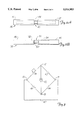
- FIG. 1 is a plan view of a wafer level test structure in accordance with the presently preferred embodiment of the present invention.
- FIGS. 2A and 2B are plan views of a first magnetoresistive element held in a single magnetic domain by shape anisotropy and a second magnetoresistive sensor held in a single magnetic domain by permanent magnets.
- FIG. 3 is a circuit diagram of the test structure of FIG. 1.
- FIGS. 4A and 4B illustrate a typical probe card used in the testing of wafers according to the present invention.
- FIGS. 5A and 5B illustrate configurations of the second magnetoresistive sensor for optimizing the test process.
- FIG. 1 illustrates a test structure 10 which may be part of a wafer on which magnetoresistive (MR) elements are fabricated. More particularly, test structure 10 may be formed on wafer substrate 12.
- Test structure 10 includes a plurality of non-magnetic, conductive film pads 20, 22, 24, 26, 28 and 30. Non-magnetic metallization contacts 32 and 34 function as bus bars to directly connect pads 20 and 26 and 24 and 30, respectively.
- the test structure is formed of ordinary wafer pads having the same configuration as the wafer pads used in production of MR elements. The six wafer pads could be reduced to four by combining pads 24 and 30 and pads 20 and 26 to accommodate the four points of a Wheatstone bridge. The use of six pads permits use of the same pad layout for all test structures, some of which require six pads.
- a first MR sensor 36 is formed between pads 22 and 24 and a second MR sensor 38 is formed between pads 28 and 30. Sensors 36 and 38 are shown in greater detail in FIGS. 2A and 2B. More particularly, sensor 36 comprises a long strip 44 of Permalloy deposited on substrate 12. The substrate may be an insulating layer of oxide or other suitable material, or it may include a magnetic shield material, such as Sendust or Permalloy under an insulator layer.
- First and second metal contacts 40 and 42 are deposited on strip 44, substrate 12 and contacting pads 22 and 24, respectively. Permalloy strip 44 bridges the space between metal contacts 40 and 42 and is held in a single domain state by its shape anisotropy. More particularly, the contacts are patterned to define an active area 45 of sensor 36 capable of producing an MR response. Hence, strip 44 and contacts 40 and 42 form a first magnetoresistive sensor which bridges between pads 22 and 24 in FIG. 1.
- sensor 38 comprises a much shorter rectangular strip 50 of Permalloy identical to the Permalloy forming strip 44.
- Permalloy strip 50 has a geometry where shape anisotropy stabilization is minimal.
- Permanent magnets 52 and 54 are deposited on or adjacent to element 50 to hold element 50 to a single domain state. For example, magnets 52 and 54 may be deposited directly onto substrate 12, or on a small residual film of element 50, or butted up directly adjacent to element 50.
- Contacts 46 and 48 are patterned to define active area 55 of sensor 38. The active areas 45 and 55 are sized identically. Metal contacts 46 and 48 provide connections of sensor 38 to pads 28 and 30, respectively. Also, as shown particularly in FIG. 1, sensors 36 and 38 form resistors R3 and R4 to the sensor circuit, shown in FIG. 3.
- sensors 36 and 38 are illustrated with having contact edges that are perpendicular to the easy axis, the edges may be slanted, like those in a barber-pole design.
- Resistor 56 is formed between pads 26 and 28.
- Resistor 56 is formed of non-magnetic material and has dimensions chosen to provide a resistance value that is nearly equal to those of one or the other of sensors 36 and 38, to facilitate the initial balance to the sensing circuit.
- Resistor 56 forms resistor R2 of the circuit of FIG. 3.
- the two magnetoresistive sensors 36 and 38 have identically sized active areas, but one is a permanent magnet stabilized sensor and the other is a sensor whose single domain state is stabilized by shape anisotropy. Sensors 36 and 38 are formed at the same time, during the same deposition processes, and using the same materials as other MR elements on the wafer, and, were they used for heads, would produce an unbiased MR response.
- the MR elements being fabricated and the test structure 10 are formed on a wafer by depositing and patterning the MR (Permalloy) material (including elements 44, 50 and 56), ion milling the MR elements, depositing the permanent magnet films 52 and 54, patterning the permanent magnets by liftoff; and depositing and patterning the contacts (including contacts 32, 34, 40, 42, 46 and 48).
- the MR elements being fabricated may be of the type held in a single magnetic domain by permanent magnets or by shape anisotropy.
- An example of a permanent magnet stabilized MR head is described in U.S.
- sensor 38 may additionally incorporate an SAL formed of ferromagnetic material such as nickel-iron-rhodium, nickel-iron-rhenium, or nickel-iron-chromium, as described in U.S. patent application Ser. No. 08/380,820 filed Jan. 30, 1995 for "Magnetoresistive Sensor with Improved Performance and Processability" by Peter I. Bonyhard, James F. Dolejsi, Charles H. Tolman and William P. Wood and assigned to the same assignee as the present invention.
- SAL soft adjacent layer
- a variable resistor R1 is attached, such as by probes, between pads 20 and 22 to form a balancing resistance to the test circuit.
- An appropriate power supply 60 (FIG. 3) is attached to pads 20 and 30, and a suitable voltmeter 62 is attached to pads 22 and 28.
- these connections may be made by a single probe assembly comprising a card having probe pins 70, 71.72 and 73.
- the probe assembly should also be equipped with field coils 64, 66 capable of generating magnetic fields of adequate strength to saturate the sensors 36 and 38, along with any shields if present. If the probe assembly does not itself contain field coils, an external magnetic field source is necessary. A magnetic field of about 100 Oe is adequate for most cases.
- FIGS. 4A and 4B illustrate opposite sides of a typical probe card used in the test.
- One example probe card is Model No. E701X8.375 available from Alphatronics Engineering Corporation of Colorado Springs, Colo.
- the probe card includes six pins mounted to one side of wafer 75 (FIG. 4A) arranged to engage pads 20, 22, 24, 26, 28 and 30 on substrate 12.
- the six pins include pins 70, 71, 72 and 73, diagrammatically illustrated in FIG. 1, to engage pads 20, 30, 22 and 28, respectively.
- the opposite side of wafer 75 (FIG. 4B) includes circuit traces connected to respective pins and terminating at terminals for connection to external equipment.
- Terminal 80 is connected to pin 70, terminal 81 is connected to pin 71, terminal 82 is connected to pin 72 and terminal 83 is connected to pin 73.
- Power source 60 (FIG. 3) is connected through terminals 80 and 81 and pins 70 and 71 to pads 20 and 30, resistor R1 is connected through terminals 80 and 82 and pins 70 and 72 to pads 20 and 22, and meter 62 is connected through terminals 82 and 83 and pins 72 and 73 to pads 22 and 28, all as illustrated in FIGS 1 and 3.
- a magnetic field (such as between about +50 and +100 Oe) is applied to the sensors so that the sensors assume a single domain state. Any small differences in resistance between sensors 36 and 38 are balanced by adjusting resistor R1.
- the magnetic field applied to sensors 36 and 38 by field coils 64 and 66 is slowly reduced and reversed (to about -20 Oe).
- the shape anisotropy stabilized sensor 36 should remain single domain during the procedure.
- the permanent magnet stabilization is inadequate, the associated MR active area of sensor 38 will become multi-domain.
- the presence of closure domains reduces the effective active area for the sensors to produce an MR response.
- the effect will likely be greater on sensor 38 than sensor 36 because sensor 36 is at least partially held to single magnetic domains by the long MR structure, whereas defects in the permanent magnet stabilizing films of sensor 38 are more likely to allow sensor 38 to develop multiple magnetic domains. Consequently, if closure domains are present, a small resistance difference will arise between sensors 36 and 38 while the magnetic field is reduced and reversed to the sensors.
- the amount of imbalance of the bridge circuit is indicative of the resistance difference due solely to differences in magnetoresistive response between sensors 36 and 38.
- Variable resistor R1 is then adjusted to restore balance to the circuit while, at the same time, measuring the resistance change required to reach balance. Because both MR sensors 36 and 38 are part of the bridge circuit, the resistance change can be measured to great precision and provides a measurement of the extent of multiple magnetic domains in the MR elements.
- FIGS. 5A and 5B illustrate various geometries of sensor 38.
- permanent magnets 52 and 54 are positioned adjacent Permalloy strip 50 with metal contacts 46 and 48 over and in contact with the permanent magnets outside the bounds between the magnets and strip 50.
- FIG. 5B shows sensor 38 with its contacts 46 and 48 extending over the bounds into direct contact with Permalloy strip 50.
- sensor 38 has dimensions a, b, and c that define the height (a) of the magnetoresistive sensing element, the width (b) of the magnetoresistive strip along the easy axis, and the distance (c) between contacts 46 and 48 along the easy axis.
- the active area therefore, is defined by the smaller dimension of b and c.
- sensor 38 may be constructed with a soft adjacent layer (SAL) of soft magnetic material adjacent strip 50, such as when the test structure is employed on wafers where SALs are formed adjacent the magnetoresistive materials of the head structures being formed on the wafer.
- SAL soft adjacent layer
- a plurality of test structures 10 may be positioned at various locations on a wafer. By applying the probe card shown in FIG. 4 to each of the test structures on the wafer, tests can be performed in a short period of time at a variety of locations on the wafer to map detective or unstable MR elements on the wafer.
- test structures 10 having different geometries of dimensions a, b, c for sensor 38
- the effectiveness of the manufacturing process for permanent magnet stabilized transducers may be mapped by charting the position of effective and stable test structure sensors on the wafer in accordance with the various geometric parameters.
- the test structure may be employed to determine the effectiveness of the manufacturing process.
- comparison of test results between several wafers may be used to determine repeatability of the manufacturing process over several wafers and to define optimal geometric parameters for the dimensions a, b, and c.
- test structure provides a mechanism for determining the effectiveness of the manufacturing process as well as optimizing the geometry of the heads being produced by the manufacturing process for purposes of high reliability and repeatability of the parameters of that head.
Landscapes
- Physics & Mathematics (AREA)
- General Physics & Mathematics (AREA)
- Chemical & Material Sciences (AREA)
- Condensed Matter Physics & Semiconductors (AREA)
- Health & Medical Sciences (AREA)
- Life Sciences & Earth Sciences (AREA)
- Analytical Chemistry (AREA)
- Biochemistry (AREA)
- General Health & Medical Sciences (AREA)
- Electrochemistry (AREA)
- Immunology (AREA)
- Pathology (AREA)
- Chemical Kinetics & Catalysis (AREA)
- Engineering & Computer Science (AREA)
- Manufacturing & Machinery (AREA)
- Measuring Magnetic Variables (AREA)
Abstract
Description
Claims (27)
Priority Applications (1)
| Application Number | Priority Date | Filing Date | Title |
|---|---|---|---|
| US08/437,692 US5514953A (en) | 1994-02-24 | 1995-05-09 | Wafer level test structure for detecting multiple domains and magnetic instability in a permanent magnet stabilized MR head |
Applications Claiming Priority (2)
| Application Number | Priority Date | Filing Date | Title |
|---|---|---|---|
| US20166694A | 1994-02-24 | 1994-02-24 | |
| US08/437,692 US5514953A (en) | 1994-02-24 | 1995-05-09 | Wafer level test structure for detecting multiple domains and magnetic instability in a permanent magnet stabilized MR head |
Related Parent Applications (1)
| Application Number | Title | Priority Date | Filing Date |
|---|---|---|---|
| US20166694A Continuation-In-Part | 1994-02-24 | 1994-02-24 |
Publications (1)
| Publication Number | Publication Date |
|---|---|
| US5514953A true US5514953A (en) | 1996-05-07 |
Family
ID=22746775
Family Applications (1)
| Application Number | Title | Priority Date | Filing Date |
|---|---|---|---|
| US08/437,692 Expired - Fee Related US5514953A (en) | 1994-02-24 | 1995-05-09 | Wafer level test structure for detecting multiple domains and magnetic instability in a permanent magnet stabilized MR head |
Country Status (1)
| Country | Link |
|---|---|
| US (1) | US5514953A (en) |
Cited By (34)
| Publication number | Priority date | Publication date | Assignee | Title |
|---|---|---|---|---|
| US6249394B1 (en) | 1999-02-12 | 2001-06-19 | International Business Machines Corporation | Method and apparatus for providing amplitude instability data recovery for AMR/GMR heads |
| US6453722B1 (en) | 1998-06-11 | 2002-09-24 | Seagate Technology Llc | Integrated test system for a disc drive pivot bearing and actuator |
| US20020138970A1 (en) * | 2001-03-30 | 2002-10-03 | Fujitsu Limited | Method of accurate evaluation on magnetoresistive read element |
| US6472866B2 (en) | 2000-02-17 | 2002-10-29 | Seagate Technologies Llc | Head stack assembly (HSA) with shunt testing access port |
| US6483298B2 (en) | 2000-06-02 | 2002-11-19 | Seagate Technology Llc | Test simulation of a read/write head |
| US20030030934A1 (en) * | 2001-08-09 | 2003-02-13 | Seagate Technology Llc | In-situ detection of transducer magnetic instability in a disc drive |
| US20030049372A1 (en) * | 1997-08-11 | 2003-03-13 | Cook Robert C. | High rate deposition at low pressures in a small batch reactor |
| US6587805B2 (en) | 2000-02-25 | 2003-07-01 | Seagate Technology Llc | Testing a write transducer as a reader |
| US6633459B2 (en) | 2000-06-20 | 2003-10-14 | Seagate Technology Llc | Functional recording-head on-slider lap monitor |
| US6661223B2 (en) | 2002-01-07 | 2003-12-09 | International Business Machines Corporation | Method of testing for response abnormalities in a magnetic sensor |
| US6798191B1 (en) | 1999-08-09 | 2004-09-28 | Power Measurement Ltd. | Revenue meter with a graphic user interface being operative to display scalable objects |
| US20060049823A1 (en) * | 2004-07-09 | 2006-03-09 | Takashi Suzuki | Probe card and method for testing magnetic sensor |
| US20090015242A1 (en) * | 2006-12-04 | 2009-01-15 | Micronas Gmbh | Method to Test the Measurement Accuracy of At Least One Magnetic Field Sensor |
| US20090167333A1 (en) * | 2007-12-31 | 2009-07-02 | Beach Robert S | Wafer level testing |
| US20090168215A1 (en) * | 2007-12-27 | 2009-07-02 | Beach Robert S | Test components fabricated with large area sensors used for determining the resistance of an mr sensor |
| US20090168216A1 (en) * | 2007-12-27 | 2009-07-02 | Beach Robert S | Test components fabricated with pseudo sensors used for determining the resistance of an mr sensor |
| US20100090680A1 (en) * | 2008-10-10 | 2010-04-15 | Electro Industries/Gauge Tech. | Intelligent electronic device having a terminal assembly for coupling to a meter mounting socket |
| US20100237345A1 (en) * | 2009-03-18 | 2010-09-23 | Tdk Corporation | Wafer and manufacturing method of electronic component |
| US8008912B1 (en) | 2008-12-16 | 2011-08-30 | Western Digital (Fremont), Llc | Method and system for testing P2 stiffness of a magnetoresistance transducer at the wafer level |
| US8653824B1 (en) | 2009-12-16 | 2014-02-18 | Western Digital (Fremont), Llc | Delta temperature test method and system |
| US20180011150A1 (en) * | 2012-05-10 | 2018-01-11 | Allegro Microsystems, Llc | Methods and apparatus for magnetic sensor having integrated coil |
| US9897461B2 (en) | 2015-02-27 | 2018-02-20 | Electro Industries/Gauge Tech | Intelligent electronic device with expandable functionality |
| US10048088B2 (en) | 2015-02-27 | 2018-08-14 | Electro Industries/Gauge Tech | Wireless intelligent electronic device |
| US10495699B2 (en) | 2013-07-19 | 2019-12-03 | Allegro Microsystems, Llc | Methods and apparatus for magnetic sensor having an integrated coil or magnet to detect a non-ferromagnetic target |
| US10670672B2 (en) | 2013-07-19 | 2020-06-02 | Allegro Microsystems, Llc | Method and apparatus for magnetic sensor producing a changing magnetic field |
| US10725100B2 (en) | 2013-03-15 | 2020-07-28 | Allegro Microsystems, Llc | Methods and apparatus for magnetic sensor having an externally accessible coil |
| US10837943B2 (en) | 2017-05-26 | 2020-11-17 | Allegro Microsystems, Llc | Magnetic field sensor with error calculation |
| US10996289B2 (en) | 2017-05-26 | 2021-05-04 | Allegro Microsystems, Llc | Coil actuated position sensor with reflected magnetic field |
| US11009922B2 (en) | 2015-02-27 | 2021-05-18 | Electro Industries/Gaugetech | Wireless intelligent electronic device |
| US11262422B2 (en) | 2020-05-08 | 2022-03-01 | Allegro Microsystems, Llc | Stray-field-immune coil-activated position sensor |
| US11307054B2 (en) | 2014-10-31 | 2022-04-19 | Allegro Microsystems, Llc | Magnetic field sensor providing a movement detector |
| US11428755B2 (en) | 2017-05-26 | 2022-08-30 | Allegro Microsystems, Llc | Coil actuated sensor with sensitivity detection |
| US11493361B2 (en) | 2021-02-26 | 2022-11-08 | Allegro Microsystems, Llc | Stray field immune coil-activated sensor |
| US11578997B1 (en) | 2021-08-24 | 2023-02-14 | Allegro Microsystems, Llc | Angle sensor using eddy currents |
Citations (2)
| Publication number | Priority date | Publication date | Assignee | Title |
|---|---|---|---|---|
| US5247276A (en) * | 1990-04-25 | 1993-09-21 | Daito Communication Apparatus Co., Ltd. | Ptc device |
| US5260653A (en) * | 1992-06-03 | 1993-11-09 | Eastman Kodak Company | Thin film very high sensitivity magnetoresistive magnetometer having temperature compensation and simple domain stability |
-
1995
- 1995-05-09 US US08/437,692 patent/US5514953A/en not_active Expired - Fee Related
Patent Citations (2)
| Publication number | Priority date | Publication date | Assignee | Title |
|---|---|---|---|---|
| US5247276A (en) * | 1990-04-25 | 1993-09-21 | Daito Communication Apparatus Co., Ltd. | Ptc device |
| US5260653A (en) * | 1992-06-03 | 1993-11-09 | Eastman Kodak Company | Thin film very high sensitivity magnetoresistive magnetometer having temperature compensation and simple domain stability |
Cited By (52)
| Publication number | Priority date | Publication date | Assignee | Title |
|---|---|---|---|---|
| US20030049372A1 (en) * | 1997-08-11 | 2003-03-13 | Cook Robert C. | High rate deposition at low pressures in a small batch reactor |
| US6453722B1 (en) | 1998-06-11 | 2002-09-24 | Seagate Technology Llc | Integrated test system for a disc drive pivot bearing and actuator |
| US6249394B1 (en) | 1999-02-12 | 2001-06-19 | International Business Machines Corporation | Method and apparatus for providing amplitude instability data recovery for AMR/GMR heads |
| US6798191B1 (en) | 1999-08-09 | 2004-09-28 | Power Measurement Ltd. | Revenue meter with a graphic user interface being operative to display scalable objects |
| US6472866B2 (en) | 2000-02-17 | 2002-10-29 | Seagate Technologies Llc | Head stack assembly (HSA) with shunt testing access port |
| US6587805B2 (en) | 2000-02-25 | 2003-07-01 | Seagate Technology Llc | Testing a write transducer as a reader |
| US6483298B2 (en) | 2000-06-02 | 2002-11-19 | Seagate Technology Llc | Test simulation of a read/write head |
| US6633459B2 (en) | 2000-06-20 | 2003-10-14 | Seagate Technology Llc | Functional recording-head on-slider lap monitor |
| US7197813B2 (en) * | 2001-03-30 | 2007-04-03 | Fujitsu Limited | Method of accurate evaluation on magnetoresistive read element |
| US20020138970A1 (en) * | 2001-03-30 | 2002-10-03 | Fujitsu Limited | Method of accurate evaluation on magnetoresistive read element |
| US20030030934A1 (en) * | 2001-08-09 | 2003-02-13 | Seagate Technology Llc | In-situ detection of transducer magnetic instability in a disc drive |
| US6661223B2 (en) | 2002-01-07 | 2003-12-09 | International Business Machines Corporation | Method of testing for response abnormalities in a magnetic sensor |
| US20060049823A1 (en) * | 2004-07-09 | 2006-03-09 | Takashi Suzuki | Probe card and method for testing magnetic sensor |
| US7345470B2 (en) * | 2004-07-09 | 2008-03-18 | Yamaha Corporation | Probe card and method for testing magnetic sensor |
| US20080106257A1 (en) * | 2004-07-09 | 2008-05-08 | Yamaha Corporation | Probe card and method for testing magnetic sensor |
| US8558537B2 (en) * | 2006-12-04 | 2013-10-15 | Micronas Gmbh | Method to test the measurement accuracy of at least one magnetic field sensor using a semiconductor chip having a measurement coil |
| US20090015242A1 (en) * | 2006-12-04 | 2009-01-15 | Micronas Gmbh | Method to Test the Measurement Accuracy of At Least One Magnetic Field Sensor |
| US20090168215A1 (en) * | 2007-12-27 | 2009-07-02 | Beach Robert S | Test components fabricated with large area sensors used for determining the resistance of an mr sensor |
| US20090168216A1 (en) * | 2007-12-27 | 2009-07-02 | Beach Robert S | Test components fabricated with pseudo sensors used for determining the resistance of an mr sensor |
| US7855553B2 (en) | 2007-12-27 | 2010-12-21 | Hitachi Global Storage Technologies Netherlands, B.V. | Test components fabricated with large area sensors used for determining the resistance of an MR sensor |
| US7932717B2 (en) | 2007-12-27 | 2011-04-26 | Hitachi Global Storage Technologies Netherlands, B.V. | Test components fabricated with pseudo sensors used for determining the resistance of an MR sensor |
| US7999566B2 (en) | 2007-12-31 | 2011-08-16 | Hitachi Global Storage Technologies, Netherlands B.V. | Wafer level testing |
| US20090167333A1 (en) * | 2007-12-31 | 2009-07-02 | Beach Robert S | Wafer level testing |
| US20100090680A1 (en) * | 2008-10-10 | 2010-04-15 | Electro Industries/Gauge Tech. | Intelligent electronic device having a terminal assembly for coupling to a meter mounting socket |
| US8717007B2 (en) | 2008-10-10 | 2014-05-06 | Electro Industries/Gauge Tech | Intelligent electronic device having a terminal assembly for coupling to a meter mounting socket |
| US8008912B1 (en) | 2008-12-16 | 2011-08-30 | Western Digital (Fremont), Llc | Method and system for testing P2 stiffness of a magnetoresistance transducer at the wafer level |
| US8021712B2 (en) * | 2009-03-18 | 2011-09-20 | Tdk Corporation | Wafer and manufacturing method of electronic component |
| US20100237345A1 (en) * | 2009-03-18 | 2010-09-23 | Tdk Corporation | Wafer and manufacturing method of electronic component |
| US8653824B1 (en) | 2009-12-16 | 2014-02-18 | Western Digital (Fremont), Llc | Delta temperature test method and system |
| US20180011150A1 (en) * | 2012-05-10 | 2018-01-11 | Allegro Microsystems, Llc | Methods and apparatus for magnetic sensor having integrated coil |
| US11680996B2 (en) * | 2012-05-10 | 2023-06-20 | Allegro Microsystems, Llc | Methods and apparatus for magnetic sensor having integrated coil |
| US10725100B2 (en) | 2013-03-15 | 2020-07-28 | Allegro Microsystems, Llc | Methods and apparatus for magnetic sensor having an externally accessible coil |
| US12061246B2 (en) | 2013-07-19 | 2024-08-13 | Allegro Microsystems, Llc | Method and apparatus for magnetic sensor producing a changing magnetic field |
| US11313924B2 (en) | 2013-07-19 | 2022-04-26 | Allegro Microsystems, Llc | Method and apparatus for magnetic sensor producing a changing magnetic field |
| US10495699B2 (en) | 2013-07-19 | 2019-12-03 | Allegro Microsystems, Llc | Methods and apparatus for magnetic sensor having an integrated coil or magnet to detect a non-ferromagnetic target |
| US10670672B2 (en) | 2013-07-19 | 2020-06-02 | Allegro Microsystems, Llc | Method and apparatus for magnetic sensor producing a changing magnetic field |
| US11307054B2 (en) | 2014-10-31 | 2022-04-19 | Allegro Microsystems, Llc | Magnetic field sensor providing a movement detector |
| US11009922B2 (en) | 2015-02-27 | 2021-05-18 | Electro Industries/Gaugetech | Wireless intelligent electronic device |
| US11644341B2 (en) | 2015-02-27 | 2023-05-09 | El Electronics Llc | Intelligent electronic device with hot swappable battery |
| US12087998B2 (en) | 2015-02-27 | 2024-09-10 | Ei Electronics Llc | Wireless intelligent electronic device |
| US9897461B2 (en) | 2015-02-27 | 2018-02-20 | Electro Industries/Gauge Tech | Intelligent electronic device with expandable functionality |
| US10739162B2 (en) | 2015-02-27 | 2020-08-11 | Electro Industries/Gauge Tech | Intelligent electronic device with surge supression |
| US10274340B2 (en) | 2015-02-27 | 2019-04-30 | Electro Industries/Gauge Tech | Intelligent electronic device with expandable functionality |
| US10048088B2 (en) | 2015-02-27 | 2018-08-14 | Electro Industries/Gauge Tech | Wireless intelligent electronic device |
| US11641052B2 (en) | 2015-02-27 | 2023-05-02 | El Electronics Llc | Wireless intelligent electronic device |
| US10996289B2 (en) | 2017-05-26 | 2021-05-04 | Allegro Microsystems, Llc | Coil actuated position sensor with reflected magnetic field |
| US11428755B2 (en) | 2017-05-26 | 2022-08-30 | Allegro Microsystems, Llc | Coil actuated sensor with sensitivity detection |
| US11768256B2 (en) | 2017-05-26 | 2023-09-26 | Allegro Microsystems, Llc | Coil actuated sensor with sensitivity detection |
| US10837943B2 (en) | 2017-05-26 | 2020-11-17 | Allegro Microsystems, Llc | Magnetic field sensor with error calculation |
| US11262422B2 (en) | 2020-05-08 | 2022-03-01 | Allegro Microsystems, Llc | Stray-field-immune coil-activated position sensor |
| US11493361B2 (en) | 2021-02-26 | 2022-11-08 | Allegro Microsystems, Llc | Stray field immune coil-activated sensor |
| US11578997B1 (en) | 2021-08-24 | 2023-02-14 | Allegro Microsystems, Llc | Angle sensor using eddy currents |
Similar Documents
| Publication | Publication Date | Title |
|---|---|---|
| US5514953A (en) | Wafer level test structure for detecting multiple domains and magnetic instability in a permanent magnet stabilized MR head | |
| EP0286079B1 (en) | Sensing devices utilizing magneto electric transducers | |
| US7098655B2 (en) | Eddy-current sensor with planar meander exciting coil and spin valve magnetoresistive element for nondestructive testing | |
| JP4105142B2 (en) | Current sensor | |
| US6504363B1 (en) | Sensor for eddy current testing and method of use thereof | |
| US5901001A (en) | Detection of asperities in recording surface of storage medium | |
| US6538430B2 (en) | Screening test for transverse magnetic-field excited noise in giant magnetoresistive heads | |
| US6265885B1 (en) | Method, apparatus and computer program product for identifying electrostatic discharge damage to a thin film device | |
| US6534974B1 (en) | Magnetic head tester with write coil and read coil | |
| US6515475B2 (en) | Determination of track width of magnetoresistive sensors during magnetic head fabrication using magnetic fields | |
| US4048557A (en) | Planar magnetoresistance thin film probe for magnetic field alignment | |
| US6294911B1 (en) | Measurement method of magnetization direction of magnetoresistive effect devices and measurement apparatus based on the method of TDK corporation | |
| US6433540B1 (en) | Method and apparatus for testing composite type magnetic head having a magnetoresistive element and an inductive element | |
| US5390420A (en) | MR element-to-contact alignment test structure | |
| US4100609A (en) | Magnetoresistance detector for crosstie memories | |
| JP2008065898A (en) | Method for evaluating magnetoresistive read head | |
| US6859678B1 (en) | Method and apparatus for manufacturing magnetoresistive element, software and system for controlling manufacturing of magnetoresistive element, software for estimating resistance value of magnetoresistive element, and computer system | |
| JP3369186B2 (en) | Peak magnetic field detector with non-volatile storage | |
| JP3835155B2 (en) | Inspection method and apparatus for magnetic head having magnetoresistive effect element | |
| JP3717628B2 (en) | Method and apparatus for evaluating magnetoresistive head | |
| US4683535A (en) | Thin film magnetometer | |
| US7138797B2 (en) | Reverse magnetic reset to screen for weakly pinned heads | |
| US5629620A (en) | Apparatus and method for measurement of magnetic remanence-thickness product of thin magnetic layers | |
| KR920003481B1 (en) | Method of manufacturing thin film magnetic head | |
| JP3101793B2 (en) | DC resistance inspection method for magnetoresistive head |
Legal Events
| Date | Code | Title | Description |
|---|---|---|---|
| AS | Assignment |
Owner name: SEAGATE TECHNOLOGY, INC., MINNESOTA Free format text: ASSIGNMENT OF ASSIGNORS INTEREST;ASSIGNORS:SCHULTZ, ALLAN E.;GEORGE, PETER K.;WOOD, WILLIAM P.;AND OTHERS;REEL/FRAME:007514/0823 Effective date: 19950426 |
|
| CC | Certificate of correction | ||
| FPAY | Fee payment |
Year of fee payment: 4 |
|
| FEPP | Fee payment procedure |
Free format text: PAYOR NUMBER ASSIGNED (ORIGINAL EVENT CODE: ASPN); ENTITY STATUS OF PATENT OWNER: LARGE ENTITY |
|
| AS | Assignment |
Owner name: SEAGATE TECHNOLOGY LLC, CALIFORNIA Free format text: ASSIGNMENT OF ASSIGNORS INTEREST;ASSIGNOR:SEAGATE TECHNOLOGY, INC.;REEL/FRAME:011077/0319 Effective date: 20000728 |
|
| AS | Assignment |
Owner name: THE CHASE MANHATTAN BANK, AS COLLATERAL AGENT, NEW Free format text: SECURITY AGREEMENT;ASSIGNOR:SEAGATE TECHNOLOGY LLC;REEL/FRAME:011461/0001 Effective date: 20001122 |
|
| AS | Assignment |
Owner name: JPMORGAN CHASE BANK, AS COLLATERAL AGENT, NEW YORK Free format text: SECURITY AGREEMENT;ASSIGNOR:SEAGATE TECHNOLOGY LLC;REEL/FRAME:013177/0001 Effective date: 20020513 Owner name: JPMORGAN CHASE BANK, AS COLLATERAL AGENT,NEW YORK Free format text: SECURITY AGREEMENT;ASSIGNOR:SEAGATE TECHNOLOGY LLC;REEL/FRAME:013177/0001 Effective date: 20020513 |
|
| REMI | Maintenance fee reminder mailed | ||
| LAPS | Lapse for failure to pay maintenance fees | ||
| FP | Lapsed due to failure to pay maintenance fee |
Effective date: 20040507 |
|
| AS | Assignment |
Owner name: SEAGATE TECHNOLOGY LLC, CALIFORNIA Free format text: RELEASE OF SECURITY INTERESTS IN PATENT RIGHTS;ASSIGNOR:JPMORGAN CHASE BANK, N.A. (FORMERLY KNOWN AS THE CHASE MANHATTAN BANK AND JPMORGAN CHASE BANK), AS ADMINISTRATIVE AGENT;REEL/FRAME:016937/0554 Effective date: 20051130 |
|
| STCH | Information on status: patent discontinuation |
Free format text: PATENT EXPIRED DUE TO NONPAYMENT OF MAINTENANCE FEES UNDER 37 CFR 1.362 |