US5412353A - Phase-locked loop frequency modulation circuit for input modulation signals having low-frequency content - Google Patents
Phase-locked loop frequency modulation circuit for input modulation signals having low-frequency content Download PDFInfo
- Publication number
- US5412353A US5412353A US08/152,445 US15244593A US5412353A US 5412353 A US5412353 A US 5412353A US 15244593 A US15244593 A US 15244593A US 5412353 A US5412353 A US 5412353A
- Authority
- US
- United States
- Prior art keywords
- signal
- frequency
- input modulation
- phase
- compensation
- Prior art date
- Legal status (The legal status is an assumption and is not a legal conclusion. Google has not performed a legal analysis and makes no representation as to the accuracy of the status listed.)
- Expired - Lifetime
Links
- 230000000694 effects Effects 0.000 claims abstract description 4
- 238000006243 chemical reaction Methods 0.000 claims description 8
- 238000001914 filtration Methods 0.000 claims description 3
- 230000005540 biological transmission Effects 0.000 abstract description 3
- 230000001413 cellular effect Effects 0.000 abstract description 3
- 238000004891 communication Methods 0.000 abstract description 2
- 238000010586 diagram Methods 0.000 description 4
- 238000000034 method Methods 0.000 description 1
Images

Classifications
-
- H—ELECTRICITY
- H03—ELECTRONIC CIRCUITRY
- H03C—MODULATION
- H03C3/00—Angle modulation
- H03C3/02—Details
- H03C3/09—Modifications of modulator for regulating the mean frequency
- H03C3/0908—Modifications of modulator for regulating the mean frequency using a phase locked loop
- H03C3/095—Modifications of modulator for regulating the mean frequency using a phase locked loop applying frequency modulation to the loop in front of the voltage controlled oscillator
-
- H—ELECTRICITY
- H03—ELECTRONIC CIRCUITRY
- H03L—AUTOMATIC CONTROL, STARTING, SYNCHRONISATION OR STABILISATION OF GENERATORS OF ELECTRONIC OSCILLATIONS OR PULSES
- H03L7/00—Automatic control of frequency or phase; Synchronisation
- H03L7/06—Automatic control of frequency or phase; Synchronisation using a reference signal applied to a frequency- or phase-locked loop
- H03L7/08—Details of the phase-locked loop
- H03L7/085—Details of the phase-locked loop concerning mainly the frequency- or phase-detection arrangement including the filtering or amplification of its output signal
- H03L7/093—Details of the phase-locked loop concerning mainly the frequency- or phase-detection arrangement including the filtering or amplification of its output signal using special filtering or amplification characteristics in the loop
Definitions
- the present invention generally pertains to phase-locked loop frequency modulation circuits and is particularly directed to frequency modulation with an input modulation signal having a low-frequency content.
- a typical prior art phase-locked loop frequency modulation circuit includes a voltage controlled oscillator (VCO) 10, a frequency divider 12, a phase detector 14, a loop filter 16 and an adder 18.
- VCO voltage controlled oscillator
- the VCO 10 provides an output signal 20 having a given frequency in accordance with the voltage of a control signal 22 provided to the input of the VCO 10.
- the frequency divider 12 divides the given frequency of the VCO output signal 20 by an integer N to provide a frequency-divided VCO output signal 24 having a frequency that is near the frequency f REF of a reference frequency signal 26.
- the phase detector 14 compares the phase of the frequency-divided VCO output signal 24 with the phase of the reference frequency signal 26 to provide a phase error signal 28 that is indicative of a phase difference between the reference frequency signal 26 and the VCO output signal 20.
- the loop filter 16 filters the phase error signal 28 to provide a loop filter output signal 30.
- the adder 18 adds the loop filter output signal 30 to an input modulation signal 32 having a content m(t) to provide the control signal 22 that is provided to the input of the VCO 10 to frequency modulate the output signal 20 that is provided by the VCO 10 at the given frequency.
- the given frequency of the VCO output signal 20 may be centered at the frequency of a broadcast transmission channel or at some intermediate frequency.
- Phase-locked loop frequency modulation circuits are used in many applications, including radios for cellular broadcast systems.
- the content m(t) of the input modulation signal 32 is a voltage that varies in amplitude.
- a typical phase-locked loop frequency modulation circuit performs satisfactorily when the input modulation signal has its content m(t) derived from a voice signal
- the transfer function of a typical phase-locked loop frequency modulation circuit is such that the typical circuit does not perform satisfactorily when the input modulation signal has its content m(t) derived from a data signal having a significant low-frequency content, i.e. a data signal having significant energy at frequencies approaching DC, which occurs for a digital data signal when there is an uneven distribution of one-bits and zero-bits .
- the transfer function of the typical phase-locked loop frequency modulation circuit as shown in FIG. 1, is:
- K o is the gain of the VCO
- K d is the gain of the phase detector
- ⁇ is proportional to frequency
- This transfer function goes to zero as s goes to zero, which means that the phase-locked loop does not pass the low-frequency content of the input modulation signal, whereby for a digital data signal having an uneven distribution of one-bits and zero-bits, the bit error performance is degraded.
- a solution to this problem is to provide a phase-locked loop frequency modulation circuit having a transfer function that is constant for all frequencies. This will occur if the transfer function is:
- Phase-locked loop frequency modulation circuits having constant transfer functions have been described in U.S. Pat. Nos. 4,052,672 to Enderby et al. and 4,242,649 to Washburn, Jr. Enderby et al. described further adding an integrated input modulation signal to the phase error signal at the input of the loop filter; and Washburn, Jr. described further adding a compensated input modulation signal to the phase error signal at the input of the loop filter, with the compensated input modulation signal being provided by processing the input modulation signal to compensate for the transfer functions of the loop components. Washburn, Jr. also alternatively described adding the compensated input modulation signal into the loop at the first node available after the input to the loop filter when an integrated circuit in which the phase-locked loop is embodied does not have an available pin at the input of the loop filter.
- the present invention provides a frequency-modulation circuit, comprising a phase-locked loop, including a voltage controlled oscillator (VCO) for providing an output signal having a given frequency; means for adding a compensation signal to a loop filter output signal to provide a control signal to the VCO for controlling the frequency of the VCO output signal; means for processing an output signal from the VCO with a reference frequency signal to provide a phase error signal indicative of a phase difference between the reference frequency signal and the VCO output signal; and a loop filter having a predetermined transfer function for filtering the phase error signal to provide the loop filter output signal that is added to the compensation signal; and a compensation circuit for processing an input modulation signal to provide the compensation signal that is added to the loop filter output signal by processing the input modulation signal to provide the same effect as adding the input modulation signal to an integrated input modulation signal that is filtered by a filter having said predetermined transfer function to provide the compensation signal.
- VCO voltage controlled oscillator
- K o is the gain of the VCO and K d is the gain of the phase detector
- the transfer function for the phase-locked loop frequency modulation circuit of the present invention is:
- the phase-locked loop frequency modulation circuit of the present invention performs frequency modulation satisfactorily even when the input modulation signal has significant energy at frequencies approaching zero.
- the frequency modulation circuit of the present invention can be constructed by combining the compensation circuit with a typical phase-locked loop.
- the frequency modulation circuit of the present invention accurately compensates for the inability of a phase-locked loop to pass low-frequency content of an input modulation signal, and may be utilized with existing communication apparatus, such as a cellular telephone voice radio, for accurate data transmission without having to modify such apparatus.
- FIG. 1 is a block diagram of a typical prior art phase-locked loop frequency modulation circuit.
- FIG. 2 is an equivalent block diagram of a phase-locked loop frequency modulation circuit according to the present invention.
- FIG. 3A illustrates the waveform of the VCO output signal produced in the frequency modulation circuit of FIG. 2.
- FIG. 3B illustrates the waveform of the phase error signal produced in the frequency modulation circuit of FIG. 2.
- FIG. 3C illustrates the waveform of the loop filter output signal produced in the frequency modulation circuit of FIG. 2.
- FIG. 3D illustrates the waveform of the input modulation signal provided to the frequency modulation circuit of FIG. 2.
- FIG. 3E illustrates the waveform of the conversion signal produced in the frequency modulation circuit of FIG. 2.
- FIG. 3F illustrates the waveform of the compensation signal produced in the frequency modulation circuit of FIG. 2.
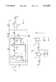
- FIG. 4 is a schematic circuit diagram of the compensation circuit in one preferred embodiment of the frequency modulation circuit of FIG. 2.
- FIG. 5 is a schematic circuit diagram of the loop filter in said one preferred embodiment of the frequency modulation circuit of FIG. 2.
- a preferred embodiment of a phase-locked loop frequency modulation circuit includes a voltage controlled oscillator (VCO) 40, a frequency divider 42, a phase detector 44, a loop filter 46, a first adder 48 and a compensation circuit 50.
- the compensation circuit 50 includes an integrator 52, a second filter 54 and a second adder 56.
- the integrator 52 has a gain A.
- the second filter 54 has the same transfer function as the loop filter 46.
- the VCO 40 provides an output signal 60 (as shown in FIG. 3A) having a given frequency in accordance with the voltage of a control signal 62 provided to the input of the VCO 40.
- the frequency divider 42 divides the given frequency of the VCO output signal 60 by an integer N to provide a frequency-divided VCO output signal 64 having a frequency that is near the frequency f REF of a reference frequency signal 66.
- the phase detector 44 compares the phase of the frequency-divided VCO output signal 64 with the phase of the reference frequency signal 66 to provide a phase error signal 68 (as shown in FIG. 3B) that is indicative of a phase difference between the reference frequency signal 66 and the VCO output signal 60.
- the loop filter 46 filters the phase error signal 28 to provide a loop filter output signal 70 (as shown in FIG. 3C).
- the integrator 52 integrates an input modulation signal 72 (as shown in FIG. 3D) and the second filter 54 filters the integrated input modulation signal 74 to provide a conversion signal 76 (as shown in FIG. 3E).
- the second adder 56 adds the conversion signal 76 to the input modulation signal 72 to provide a compensation signal 78 (as shown in FIG. 3F).
- the first adder 48 adds the loop filter output signal 70 to the compensation signal 78 to provide the control signal 62 that is provided to the input of the VCO 40 to frequency modulate the output signal 60 that is provided by the VCO 40 at the given frequency.
- the compensation circuit 50 does not include a combination of the discrete integrator 52, the second filter 54 and the second adder 56 shown in FIG. 2, but rather is constructed as shown in FIG. 4 for processing an input modulation signal provided at an input terminal 72' to provide a compensation signal at an output terminal 78'.
- the compensation circuit of FIG. 4 includes a capacitance C1 connected between an input terminal 72' and a node 80; a resistance R1 connected between the node 80 and a reference voltage terminal V REF ; a filter section 82 that includes an operational amplifier A1 having its non-inverting input terminal connected to the node 80, a capacitance C2 connected between the output terminal and the inverting input terminal of the operational amplifier A1, a resistance R2 connected in parallel with the capacitance C2, a resistance R3 connected between the inverting input terminal of the operational amplifier A1 and the reference voltage terminal V REF , a resistance R4 connected between the output terminal of the operational amplifier A1 and a node 84, and a capacitance C3 connected between the node 86 and circuit ground; a low pass filter 86 that includes a resistance R5 connected between the node 84 and a node 88, and a capacitance C4 connected between the node 88 and circuit ground; an operational amplifier A2 having its non-inverting input terminal
- the loop filter is constructed as shown in FIG. 5.
- the loop filter of FIG. 5 includes an operational amplifier A3 having its non-inverting input terminal connected to the reference voltage terminal V REF , a resistance R11 connected between the input node 68' and the inverting input terminal of the operational amplifier A3, a resistance R12 connected between the output terminal and the inverting input terminal of the operational amplifier A3, and a capacitance C6 connected in parallel with the resistance R12, an operational amplifier A4 having its non-inverting input terminal connected to the reference voltage terminal V REF , a resistance R13 connected between the output terminal of the operational amplifier A3 and the inverting input terminal of the operational amplifier A4, and a series combination of a capacitance C7 and a resistance R14 connected between the output terminal and the inverting input terminal of the operational amplifier A4.
- the compensation circuit of FIG. 4 processes an input modulation signal 72 provided at the input terminal 72' to provide the same effect as adding the input modulation signal 72 to an integrated input modulation signal that is filtered by a filter having the same transfer function as the loop filter 46 to provide the compensation signal 78.
- the loop filter shown in FIG. 5 has a predetermined transfer function f(s); and the filter section 82 of the compensation circuit shown in FIG. 4 has the same predetermined transfer function f(s).
- the combination of the resistance R5 and the capacitance C4 included in the low pass filter 84 of the compensation circuit of FIG. 4 integrates the filtered input modulation signal presented at node 86 to provide a conversion signal at node 88.
- the gain A of the compensation circuit of FIG. 4 is determined by the value of the resistance R8.
- the conversion signal is provided from the node 88 via the resistance R9 to the input terminal of the operational amplifier A2 where the conversion signal is added to the input modulation signal, which is provided from the input terminal 72' to the input terminal of the operational amplifier A2 via the capacitance C1, resistance R6 and resistance R7.
Landscapes
- Stabilization Of Oscillater, Synchronisation, Frequency Synthesizers (AREA)
- Digital Transmission Methods That Use Modulated Carrier Waves (AREA)
Abstract
Description
Δω(a)/m(s)=K.sub.o /[1+K.sub.o K.sub.d f(s)/s],(1)
Δω(s)/m(s)=K.sub.o [1+Af(s)/s]/[1+K.sub.o K.sub.d f)s)/s], (2)
Δω(s)=m(s)+[m(s)/s]AF(s)-Δω(s)[K.sub.o K.sub.d /sN]f(s), (3)
Δω(s){1+[K.sub.o K.sub.d /sN]f(s)}=m(s){1+[AF(s)]/s ]}.
Δω(s)/m(s)=K.sub.o [1+AF(s)/s]/[1+K.sub.o K.sub.d f(s)/sN ].
Claims (3)
Priority Applications (4)
| Application Number | Priority Date | Filing Date | Title |
|---|---|---|---|
| US08/152,445 US5412353A (en) | 1993-11-12 | 1993-11-12 | Phase-locked loop frequency modulation circuit for input modulation signals having low-frequency content |
| AU10533/95A AU1053395A (en) | 1993-11-12 | 1994-11-10 | Phase-locked loop frequency modulation circuit for input modulation signals having low-frequency content |
| CA002176365A CA2176365A1 (en) | 1993-11-12 | 1994-11-10 | Phase-locked loop frequency modulation circuit for input modulation signals having low-frequency content |
| PCT/US1994/012949 WO1995013651A1 (en) | 1993-11-12 | 1994-11-10 | Phase-locked loop frequency modulation circuit for input modulation signals having low-frequency content |
Applications Claiming Priority (1)
| Application Number | Priority Date | Filing Date | Title |
|---|---|---|---|
| US08/152,445 US5412353A (en) | 1993-11-12 | 1993-11-12 | Phase-locked loop frequency modulation circuit for input modulation signals having low-frequency content |
Publications (1)
| Publication Number | Publication Date |
|---|---|
| US5412353A true US5412353A (en) | 1995-05-02 |
Family
ID=22542957
Family Applications (1)
| Application Number | Title | Priority Date | Filing Date |
|---|---|---|---|
| US08/152,445 Expired - Lifetime US5412353A (en) | 1993-11-12 | 1993-11-12 | Phase-locked loop frequency modulation circuit for input modulation signals having low-frequency content |
Country Status (4)
| Country | Link |
|---|---|
| US (1) | US5412353A (en) |
| AU (1) | AU1053395A (en) |
| CA (1) | CA2176365A1 (en) |
| WO (1) | WO1995013651A1 (en) |
Cited By (15)
| Publication number | Priority date | Publication date | Assignee | Title |
|---|---|---|---|---|
| US5584062A (en) * | 1994-01-24 | 1996-12-10 | Motorola, Inc. | Method and apparatus for compensating phase locked receivers |
| US5729182A (en) * | 1994-02-11 | 1998-03-17 | Thomson-Csf | Device for continuous phase modulation by frequency synthesizer with phase-locked loop |
| US5789954A (en) * | 1995-10-25 | 1998-08-04 | Hewlett-Packard Co. | Phase dither of an acquisition clock using a delay lock loop |
| US5790942A (en) * | 1995-05-31 | 1998-08-04 | Matra Communication | Frequency modulation radio transmission device |
| US5799045A (en) * | 1994-12-22 | 1998-08-25 | Futaba Denshi Kogyo K.K. | PLL-mode radiofrequency module |
| US6008703A (en) * | 1997-01-31 | 1999-12-28 | Massachusetts Institute Of Technology | Digital compensation for wideband modulation of a phase locked loop frequency synthesizer |
| US6157260A (en) * | 1999-03-02 | 2000-12-05 | Motorola, Inc. | Method and apparatus for calibrating a local oscillator in a direct conversion receiver |
| US20020071497A1 (en) * | 2000-10-31 | 2002-06-13 | Erik Bengtsson | IQ modulation systems and methods that use separate phase and amplitude signal paths and perform modulation within a phase locked loop |
| US20030011437A1 (en) * | 2000-01-17 | 2003-01-16 | Seiichi Ozawa | Phase locked loop circuit |
| US6674331B2 (en) * | 2001-11-09 | 2004-01-06 | Agere Systems, Inc. | Method and apparatus for simplified tuning of a two-point modulated PLL |
| US6731101B2 (en) * | 2001-05-28 | 2004-05-04 | Renasas Technology Corp. | Modulation semiconductor integrated circuit device and testing method for oscillation circuit |
| US20040166813A1 (en) * | 2001-02-23 | 2004-08-26 | Mann Stephen Ian | Cartesian loop systems with digital processing |
| US20090105979A1 (en) * | 2007-10-23 | 2009-04-23 | Gerardo Escobar Valderrama | Fixed reference frame phase-locked loop (FRF-PLL) for unbalanced line voltage conditions |
| US20110221487A1 (en) * | 2003-12-17 | 2011-09-15 | Paul Lesso | Clock synchroniser |
| US20110241652A1 (en) * | 2010-03-31 | 2011-10-06 | Abb Research Ltd | Method and arrangement for estimating angular frequency |
Citations (3)
| Publication number | Priority date | Publication date | Assignee | Title |
|---|---|---|---|---|
| US4052672A (en) * | 1976-07-22 | 1977-10-04 | Motorola, Inc. | Extended phase-range, high fidelity modulator arrangement |
| US4242649A (en) * | 1979-07-13 | 1980-12-30 | Harris Corporation | Method and apparatus for modulating a phase locked loop |
| US5281930A (en) * | 1991-06-04 | 1994-01-25 | Matsushita Electric Industrial Co., Ltd. | Frequency modulator |
-
1993
- 1993-11-12 US US08/152,445 patent/US5412353A/en not_active Expired - Lifetime
-
1994
- 1994-11-10 CA CA002176365A patent/CA2176365A1/en not_active Abandoned
- 1994-11-10 AU AU10533/95A patent/AU1053395A/en not_active Abandoned
- 1994-11-10 WO PCT/US1994/012949 patent/WO1995013651A1/en active Application Filing
Patent Citations (3)
| Publication number | Priority date | Publication date | Assignee | Title |
|---|---|---|---|---|
| US4052672A (en) * | 1976-07-22 | 1977-10-04 | Motorola, Inc. | Extended phase-range, high fidelity modulator arrangement |
| US4242649A (en) * | 1979-07-13 | 1980-12-30 | Harris Corporation | Method and apparatus for modulating a phase locked loop |
| US5281930A (en) * | 1991-06-04 | 1994-01-25 | Matsushita Electric Industrial Co., Ltd. | Frequency modulator |
Cited By (21)
| Publication number | Priority date | Publication date | Assignee | Title |
|---|---|---|---|---|
| US5584062A (en) * | 1994-01-24 | 1996-12-10 | Motorola, Inc. | Method and apparatus for compensating phase locked receivers |
| US5729182A (en) * | 1994-02-11 | 1998-03-17 | Thomson-Csf | Device for continuous phase modulation by frequency synthesizer with phase-locked loop |
| US5799045A (en) * | 1994-12-22 | 1998-08-25 | Futaba Denshi Kogyo K.K. | PLL-mode radiofrequency module |
| US5790942A (en) * | 1995-05-31 | 1998-08-04 | Matra Communication | Frequency modulation radio transmission device |
| US5789954A (en) * | 1995-10-25 | 1998-08-04 | Hewlett-Packard Co. | Phase dither of an acquisition clock using a delay lock loop |
| US6008703A (en) * | 1997-01-31 | 1999-12-28 | Massachusetts Institute Of Technology | Digital compensation for wideband modulation of a phase locked loop frequency synthesizer |
| US6157260A (en) * | 1999-03-02 | 2000-12-05 | Motorola, Inc. | Method and apparatus for calibrating a local oscillator in a direct conversion receiver |
| US20030011437A1 (en) * | 2000-01-17 | 2003-01-16 | Seiichi Ozawa | Phase locked loop circuit |
| US6667663B2 (en) * | 2000-01-17 | 2003-12-23 | Fujitsu Limited | Phase locked loop circuit |
| US20020071497A1 (en) * | 2000-10-31 | 2002-06-13 | Erik Bengtsson | IQ modulation systems and methods that use separate phase and amplitude signal paths and perform modulation within a phase locked loop |
| US7072421B2 (en) * | 2000-10-31 | 2006-07-04 | Telefonaktiebolaget L.M. Ericsson | IQ modulation systems and methods that use separate phase and amplitude signal paths and perform modulation within a phase locked loop |
| US6975686B1 (en) | 2000-10-31 | 2005-12-13 | Telefonaktiebolaget L.M. Ericsson | IQ modulation systems and methods that use separate phase and amplitude signal paths |
| US20040166813A1 (en) * | 2001-02-23 | 2004-08-26 | Mann Stephen Ian | Cartesian loop systems with digital processing |
| US6731101B2 (en) * | 2001-05-28 | 2004-05-04 | Renasas Technology Corp. | Modulation semiconductor integrated circuit device and testing method for oscillation circuit |
| US6674331B2 (en) * | 2001-11-09 | 2004-01-06 | Agere Systems, Inc. | Method and apparatus for simplified tuning of a two-point modulated PLL |
| US20110221487A1 (en) * | 2003-12-17 | 2011-09-15 | Paul Lesso | Clock synchroniser |
| US8537957B2 (en) * | 2003-12-17 | 2013-09-17 | Wolfson Microelectronics Plc | Clock synchroniser |
| US20090105979A1 (en) * | 2007-10-23 | 2009-04-23 | Gerardo Escobar Valderrama | Fixed reference frame phase-locked loop (FRF-PLL) for unbalanced line voltage conditions |
| US7720623B2 (en) * | 2007-10-23 | 2010-05-18 | Instituto Potosino De Investigacion Cientifica Y Tecnologica (Ipicyt) | Fixed reference frame phase-locked loop (FRF-PLL) for unbalanced line voltage conditions |
| US20110241652A1 (en) * | 2010-03-31 | 2011-10-06 | Abb Research Ltd | Method and arrangement for estimating angular frequency |
| US8751177B2 (en) * | 2010-03-31 | 2014-06-10 | Abb Research Ltd. | Method and arrangement for estimating angular frequency |
Also Published As
| Publication number | Publication date |
|---|---|
| CA2176365A1 (en) | 1995-05-18 |
| WO1995013651A1 (en) | 1995-05-18 |
| AU1053395A (en) | 1995-05-29 |
Similar Documents
| Publication | Publication Date | Title |
|---|---|---|
| US5412353A (en) | Phase-locked loop frequency modulation circuit for input modulation signals having low-frequency content | |
| US6404277B1 (en) | Gm-C tuning circuit with filter configuration | |
| US4980653A (en) | Phase locked loop | |
| US4755774A (en) | Two-port synthesizer modulation system employing an improved reference phase modulator | |
| US6223061B1 (en) | Apparatus for low power radio communications | |
| US5052020A (en) | Method of and apparatus for controlling modulation of digital signals in frequency-modulated transmissions | |
| EP0196697B1 (en) | Am receiver | |
| US4481489A (en) | Binary signal modulating circuitry for frequency modulated transmitters | |
| GB2344006A (en) | Direct modulation phase lock loop and method therefor | |
| WO1999049569A1 (en) | Demoludator circuits | |
| US4546329A (en) | Frequency synthesizers adaptive loop filter with compensation for transients | |
| US4942374A (en) | Phase-locked loop type synthesizer having modulation function | |
| US3742361A (en) | Threshold extension phase modulated feedback receiver | |
| US5281930A (en) | Frequency modulator | |
| CA2021335C (en) | Frequency modulator | |
| US4816782A (en) | Modulation sensitivity correction circuit for voltage-controlled oscillator | |
| US6617932B2 (en) | System and method for wide dynamic range clock recovery | |
| US4601061A (en) | Automatic frequency control circuit having an equalized closed loop frequency response | |
| US4904957A (en) | Servo device for rapidly, and with low noise, locking the frequency and phase of signal to that of an imposed signal | |
| GB2234650A (en) | Fm demodulating circuit with improved noise elimination | |
| US6236689B1 (en) | Device comprising a phase-locked loop, electronic apparatus comprising such a device and method of modulating the frequency of an oscillator | |
| US4682060A (en) | Noise suppression in an I-F substitution loop | |
| JP2002508612A (en) | Demodulator circuit | |
| SU1171969A2 (en) | Frequency-phase discriminator | |
| SU1381729A1 (en) | Phase-telegraph signal demodulator |
Legal Events
| Date | Code | Title | Description |
|---|---|---|---|
| AS | Assignment |
Owner name: PACIFIC COMMUNICATION SCIENCES, INC., CALIFORNIA Free format text: ASSIGNMENT OF ASSIGNORS INTEREST;ASSIGNORS:CHAPLIK, NAOM;GARDNER, STEVEN HOLMSEN;KASMIR, SETON PAUL;REEL/FRAME:006859/0126;SIGNING DATES FROM 19940103 TO 19940105 |
|
| STCF | Information on status: patent grant |
Free format text: PATENTED CASE |
|
| CC | Certificate of correction | ||
| AS | Assignment |
Owner name: BANK OF AMERICA NATIONAL TRUST & SAVINGS ASSOCIATI Free format text: SECURITY INTEREST;ASSIGNOR:PACIFIC COMMUNICATION SCIENCES, INC.;REEL/FRAME:007936/0861 Effective date: 19960430 |
|
| AS | Assignment |
Owner name: PACIFIC COMMUNICATIONS SCIENCES, INC., CALIFORNIA Free format text: RELEASE OF SECURITY INTEREST IN CERTAIN ASSETS (PATENTS);ASSIGNOR:BANK OF AMERICA NATIONAL TRUST AND SAVINGS ASSOCIATION, AS AGENT;REEL/FRAME:008587/0343 Effective date: 19961212 |
|
| FEPP | Fee payment procedure |
Free format text: PAYOR NUMBER ASSIGNED (ORIGINAL EVENT CODE: ASPN); ENTITY STATUS OF PATENT OWNER: LARGE ENTITY |
|
| AS | Assignment |
Owner name: NUERA COMMUNICATIONS, INC., CALIFORNIA Free format text: ASSIGNMENT OF ASSIGNORS INTEREST;ASSIGNOR:PACIFIC COMMUNICATION SCIENCES, INC. (PCSI);REEL/FRAME:008811/0079 Effective date: 19971119 |
|
| FPAY | Fee payment |
Year of fee payment: 4 |
|
| FEPP | Fee payment procedure |
Free format text: PAYER NUMBER DE-ASSIGNED (ORIGINAL EVENT CODE: RMPN); ENTITY STATUS OF PATENT OWNER: LARGE ENTITY Free format text: PAYOR NUMBER ASSIGNED (ORIGINAL EVENT CODE: ASPN); ENTITY STATUS OF PATENT OWNER: LARGE ENTITY |
|
| AS | Assignment |
Owner name: CREDIT SUISSE FIRST BOSTON, NEW YORK Free format text: SECURITY INTEREST;ASSIGNORS:CONEXANT SYSTEMS, INC.;BROOKTREE CORPORATION;BROOKTREE WORLDWIDE SALES CORPORATION;AND OTHERS;REEL/FRAME:009719/0537 Effective date: 19981221 |
|
| FEPP | Fee payment procedure |
Free format text: PAYER NUMBER DE-ASSIGNED (ORIGINAL EVENT CODE: RMPN); ENTITY STATUS OF PATENT OWNER: LARGE ENTITY Free format text: PAYOR NUMBER ASSIGNED (ORIGINAL EVENT CODE: ASPN); ENTITY STATUS OF PATENT OWNER: LARGE ENTITY |
|
| AS | Assignment |
Owner name: CONEXANT SYSTEMS, INC., CALIFORNIA Free format text: RELEASE OF SECURITY INTEREST;ASSIGNOR:CREDIT SUISSE FIRST BOSTON;REEL/FRAME:012252/0413 Effective date: 20011018 Owner name: BROOKTREE CORPORATION, CALIFORNIA Free format text: RELEASE OF SECURITY INTEREST;ASSIGNOR:CREDIT SUISSE FIRST BOSTON;REEL/FRAME:012252/0413 Effective date: 20011018 Owner name: BROOKTREE WORLDWIDE SALES CORPORATION, CALIFORNIA Free format text: RELEASE OF SECURITY INTEREST;ASSIGNOR:CREDIT SUISSE FIRST BOSTON;REEL/FRAME:012252/0413 Effective date: 20011018 Owner name: CONEXANT SYSTEMS WORLDWIDE, INC., CALIFORNIA Free format text: RELEASE OF SECURITY INTEREST;ASSIGNOR:CREDIT SUISSE FIRST BOSTON;REEL/FRAME:012252/0413 Effective date: 20011018 |
|
| FPAY | Fee payment |
Year of fee payment: 8 |
|
| FPAY | Fee payment |
Year of fee payment: 12 |
|
| AS | Assignment |
Owner name: CIRRUS LOGIC INC., TEXAS Free format text: MERGER;ASSIGNOR:PACIFIC COMMUNICATION SCIENCES INC.;REEL/FRAME:045630/0333 Effective date: 20150929 |