US5249243A - Apparatus and method for cascade coupled integrated optical phase modulator for linearization of signal transfer - Google Patents
Apparatus and method for cascade coupled integrated optical phase modulator for linearization of signal transfer Download PDFInfo
- Publication number
- US5249243A US5249243A US07/886,733 US88673392A US5249243A US 5249243 A US5249243 A US 5249243A US 88673392 A US88673392 A US 88673392A US 5249243 A US5249243 A US 5249243A
- Authority
- US
- United States
- Prior art keywords
- phase modulator
- optical phase
- waveguide
- receiving
- signals
- Prior art date
- Legal status (The legal status is an assumption and is not a legal conclusion. Google has not performed a legal analysis and makes no representation as to the accuracy of the status listed.)
- Expired - Lifetime
Links
Images


Classifications
-
- G—PHYSICS
- G02—OPTICS
- G02F—OPTICAL DEVICES OR ARRANGEMENTS FOR THE CONTROL OF LIGHT BY MODIFICATION OF THE OPTICAL PROPERTIES OF THE MEDIA OF THE ELEMENTS INVOLVED THEREIN; NON-LINEAR OPTICS; FREQUENCY-CHANGING OF LIGHT; OPTICAL LOGIC ELEMENTS; OPTICAL ANALOGUE/DIGITAL CONVERTERS
- G02F1/00—Devices or arrangements for the control of the intensity, colour, phase, polarisation or direction of light arriving from an independent light source, e.g. switching, gating or modulating; Non-linear optics
- G02F1/01—Devices or arrangements for the control of the intensity, colour, phase, polarisation or direction of light arriving from an independent light source, e.g. switching, gating or modulating; Non-linear optics for the control of the intensity, phase, polarisation or colour
- G02F1/03—Devices or arrangements for the control of the intensity, colour, phase, polarisation or direction of light arriving from an independent light source, e.g. switching, gating or modulating; Non-linear optics for the control of the intensity, phase, polarisation or colour based on ceramics or electro-optical crystals, e.g. exhibiting Pockels effect or Kerr effect
- G02F1/0327—Operation of the cell; Circuit arrangements
-
- G—PHYSICS
- G02—OPTICS
- G02F—OPTICAL DEVICES OR ARRANGEMENTS FOR THE CONTROL OF LIGHT BY MODIFICATION OF THE OPTICAL PROPERTIES OF THE MEDIA OF THE ELEMENTS INVOLVED THEREIN; NON-LINEAR OPTICS; FREQUENCY-CHANGING OF LIGHT; OPTICAL LOGIC ELEMENTS; OPTICAL ANALOGUE/DIGITAL CONVERTERS
- G02F1/00—Devices or arrangements for the control of the intensity, colour, phase, polarisation or direction of light arriving from an independent light source, e.g. switching, gating or modulating; Non-linear optics
- G02F1/29—Devices or arrangements for the control of the intensity, colour, phase, polarisation or direction of light arriving from an independent light source, e.g. switching, gating or modulating; Non-linear optics for the control of the position or the direction of light beams, i.e. deflection
- G02F1/31—Digital deflection, i.e. optical switching
- G02F1/313—Digital deflection, i.e. optical switching in an optical waveguide structure
- G02F1/3136—Digital deflection, i.e. optical switching in an optical waveguide structure of interferometric switch type
-
- G—PHYSICS
- G02—OPTICS
- G02F—OPTICAL DEVICES OR ARRANGEMENTS FOR THE CONTROL OF LIGHT BY MODIFICATION OF THE OPTICAL PROPERTIES OF THE MEDIA OF THE ELEMENTS INVOLVED THEREIN; NON-LINEAR OPTICS; FREQUENCY-CHANGING OF LIGHT; OPTICAL LOGIC ELEMENTS; OPTICAL ANALOGUE/DIGITAL CONVERTERS
- G02F2203/00—Function characteristic
- G02F2203/19—Function characteristic linearised modulation; reduction of harmonic distortions
Definitions
- This invention relates generally to modulators, and more particularly to a method and apparatus for providing linearized signal transfer in integrated electro-optical phase modulators.
- Integrated electro-optical modulators are finding increasing use in state-of-the-art analog optical-fiber communication systems. Such systems are being developed as an alternative to conventional electromagnetic transmission lines.
- Present optical-fiber communication systems may consist of a high power, low noise laser source in conjunction with a wide bandwidth external modulator, for example.
- external modulators may be used in conjunction with high power, low noise lasers, to provide analog signal transfer in optical fiber cable T.V. networks.
- a common problem in such systems is that the dynamic range thereof is limited by intermodulation distortion, and by harmonic distortion due to modulator nonlinearities. Many attempts have been made in the art to improve the linearity of the modulators.
- One method of improving the linearity of optical modulators is to provide electromagnetic predistortion of the input signal.
- a system for accomplishing this is reported in an article by R. P. Childs and D. A. O'Byrne, that appeared in OFC 90, entitled "Predistortion Linearization of Directly Modulated DFB Lasers and External Modulators for AM Video Transmission.”
- Johnson U.S. Pat. Nos. 5,015,053 and 5,002,355 refer to linearization of an interferometric modulator by coupling to transverse electric (TE) and transverse magnetic (TM) modes.
- a carrier wave derived from a light source is polarized by a polarizer for adjusting the power of the carrier wave in the TE and TM polarization modes.
- Hamilton et al. U.S. Pat. No. 5,010,346 shows an electro-optical analog-to-digital converter.
- a laser light source is synchronized with a digital clock for producing pulses of light.
- the pulses of light are modulated by an optical modulator for varying the intensity of the pulses of light as a function of the amplitude of the analog modulating signal.
- the light pulses are demultiplexed and passed through a detector for converting the light pulses to electrical signals.
- the electrical signals are then passed through an electrical analog-to-digital converter.
- DuPuy et al U.S. Pat. No. 4,997,245 shows optical switches that are polarization independent.
- the optical switches include a substrate of electro-optic material in which waveguides are formed in a manner permitting light waves to be switched therethrough independent of polarization phenomena.
- Thylen U.S. Pat. No. 4,993,798 refers to an optical communication system consisting of a semiconductor laser that includes an optical waveguide coupled at one end to first and second optical directional switches. The other ends of each one of the directional couplers each have an end of a waveguide terminated to a mirror, for forming a cavity including the laser diode. By either modulating current driving the diode, or by applying a modulating signal to the directional couplers, a light signal passing therethrough can be modulated.
- Yoon et al U.S. Pat. No. 4,936,645 shows a polarization-insensitive Mach-Zehnder modulator that includes a thin film waveguide on a substrate.
- the modulator consists of a lamination of different organic polymers upon which the thin film waveguide is deposited, and electrodes for applying voltages for producing electric fields to coact with the light passing through the waveguides.
- Koai U.S. Pat. No. 4,934,776 teaches the combination of cascaded individual waveguide directional coupler sections arranged to provide a high-density optical data array, for forming an integrated optical intensity modulator.
- the cascaded coupled-waveguide modulators provide ultra-high extinction ratios.
- Koai U.S. Pat. No. 4,934,775 shows an optical space-division switching architecture consisting of high-extinction electro-optical data arrays of a plurality of cascaded coupled-waveguide optical intensity modulators.
- a plurality of passive splitter circuits are used to evenly divide an input optical signal into a plurality of interim optical signals.
- the optical signals are passed through the optical intensity modulators, respectively, which have waveguide coupler sections cascaded together on a crystal substrate to form a bar-type modulator structure, for providing a direct optical connection between the various sections of each modulator.
- Combiner circuits receive the output optical signals from the data arrays and combine them for providing a single output wave or signal.
- Coleman U.S. Pat. No. 4,882,775 shows a demodulator provided by a an interferometer and a signal processor.
- the demodulator is included in a coherence multiplexed, optical data transmission system.
- the optical data transmission system includes an interferometric modulator at an input end.
- the output signals therefrom are modulated waveforms which are passed through an optical multiplexer, and coupled via single mode optical couplers and a fiber optic cable to demodulator stages.
- Each modulator and demodulator stage is provided by an unequal arm-length Mach-Zehnder interferometer.
- the multiplexers phase modulate the optical carriers from the modulators for multiplexing the same together.
- the path lengths between the modulators and demodulators included in the system are controlled for obtaining a desired output from the output demodulator stages 40.
- U.S. Pat. No. 4,390,236 shows an electro-optical demultiplexer consisting of a plurality of cascaded tunable, polarization independent optical wavelength filters.
- the various sections of the filters, as cascaded, provide an input polarization selective coupler that separates the transverse electrical (TE) and transverse magnetic (TM) orthogonally polarized wave components, respectively, of an arbitrarily polarized input signal.
- the separated TE and TM components then travel along two different wavepaths or waveguides.
- Each waveguide includes a wavelength selective mode converter.
- An output polarization selective coupler is provided for combining in one output waveguide signal components centered about the wavelength of the mode converters, and for combining in a second output waveguide the balance of the input signal.
- Papuchon U.S. Pat. No. 4,223,977 shows an integrated optical circuit for separating a plurality of optical waves of different wavelengths, thereby providing a demultiplexing function.
- a plurality of basic electro-optical cells are integrated on a single substrate for providing the optical demultiplexing circuit.
- a paper entitled "Waveguide Modulators with Extended Linear Dynamic Range a Theoretical Prediction” shows a modified-directional-coupler modulator with reduced nonlinear distortion.
- the coupler includes an input stage for receiving input signals for a voltage control directional coupler that couples the signals to a Mach-Zehnder interferometer.
- the output of the interferometer is coupled by a fixed directional coupler to an output waveguide providing two channels. The parameters are adjusted for minimizing third order intermodulation spurious signals.
- a paper entitled "In Search of a Linear Electro-optic Amplitude Modulator" shows a linear electro-optic amplitude modulator.
- the modulator includes a Y-branch for dividing an optical input signal equally for inputting into the two arms, respectively, of a Mach-Zehnder interferometer.
- the interferometer functions as a phase shifter.
- the output of the interferometer is supplied to a directional coupler having a nominal coupling constant-length product of half a coupling length.
- the optical output signal is provided at each of two output waveguides.
- a modulation signal of one polarity is applied to the interferometer phase shifter, and is applied in reverse polarity to the directional coupler using a multiplication factor.
- the parameters are adjusted for optimizing the linearity of the modulator by reducing the second and third order harmonics that cause nonlinearities to occur.
- the present inventor recognized that known integrated optics modulators require further improvement.
- One need recognized is to improve the linearity of integrated optical phase modulators.
- An object of the present invention is to provide an improved integrated optical phase modulator with complementary output signals.
- Another object of the invention is to provide an integrated optical phase modulator having increased linearity and complementary output signals.
- an integrated optical phase modulator including a Y-branch power splitter for receiving a light input signal, splitting the same into two output signals, and passing the output signals to a first phase modulator controlled by a signal voltage V 1 (t).
- a pair of output signals from the first phase modulator are corrected as input signals via a first fixed, coupler with coupling angle Y to a second phase modulator controlled by a signal voltage V 2 (t).
- a pair of output signals from the second phase modulator are connected as input signals to second fixed coupler with coupling angle ⁇ , the latter providing complementary output signals of the cascaded modulator.
- a 3 dB coupler is substituted for the Y-branch power splitter.
- FIG. 1 is a simplified pictorial diagram showing a linearized single coupler with one rf input for one embodiment of the invention
- FIG. 2 is a plot or curve of the transfer function for optimized linear operation of the single coupler of FIG. 1;
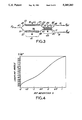
- FIG. 3 is a simplified pictorial diagram of a phase modulator ⁇ coupler cascade switch for an embodiment of the invention
- FIG. 4 is a curve showing the coupling angle ⁇ as a function of rf weighting for the phase modulator of FIG. 3;
- FIG. 5 is a curve showing the relative sensitivity as a function of rf weighting for the phase modulator of FIG. 3;
- FIG. 7 is a curve showing the third harmonic suppression (dB) as a function of modulation index m (dB) for the phase modulator-coupler cascade of FIG. 3;
- FIG. 8 shows a simplified pictorial diagram of cascaded rf phase modulators of one embodiment of the invention
- FIG. 9 is a curve showing the relative coupling angle ( ⁇ /90) as a function of rf weighting for the cascaded modulators of FIG. 8;
- FIG. 10 is a curve showing the relative rf sensitivity as a function of rf weighting for the cascaded modulators of FIG. 8;
- FIG. 12 is a curve showing the third harmonic suppression as a function of modulating index m for the cascaded modulators of FIG. 8;
- FIG. 13 shows a simplified pictorial diagram of cascaded rf phase modulators for another embodiment of the invention.
- FIG. 14 shows a simplified pictorial diagram of cascaded rf phase modulators for a preferred embodiment of the invention.
- FIG. 15 shows a simplified schematic and pictorial diagram of an engineering prototype for the embodiment of FIG. 14.
- linearized optical phase modulator embodiments of the present invention may be considered linearized optical guided waveguide (OGW) modulators.
- OGW optical guided waveguide
- each provides two complementary light output signals which offers advantages over prior modulators having only a single output signal
- the complementary output signals are substantially of the same power level and are equally linear, thereby splitting the available laser power.
- one of the complementary output signals may be used as a control signal, preferably in a closed loop system, for providing a bias adjustment to optimize and stabilize the linearity of the cascaded modulators.
- FIG. 1 an improved linearized single coupler 1, having a single rf terminal 3 for receiving an rf input signal rf(x) is shown.
- coupler 1 includes two cascaded sections 5 and 7 having coupler lengths l 1 and l 2 , respectively.
- An upper horizontal waveguide segment 9 conducts a light input signal a in to a downward sloping waveguide segment 11 for providing an input laser light signal to the coupler 1.
- the first coupler section 5 includes in the integrated structure shown a portion of a horizontal waveguide segment 17 for receiving light input signal a in from waveguide segment 11, a portion of a lower waveguide segment 19 connected at one end to an output end of waveguide segment 15, an electrode 21 overlying an associated portion of waveguide 17, and an electrode 23 overlying an associated portion of waveguide 19.
- the terminal 3 is connected to electrode 21 for providing the rf signal rf(x) thereto.
- Electrode 23 is connected to a source of reference potential, ground in this example. Note that waveguides 17 and 19 are substantially parallel to one another as are electrodes 21 and 23.
- the second coupler section 7 includes the remaining portions of waveguide segments 17 and 19, in this example.
- An electrode 25 overlies an associated portion of waveguide 17.
- An electrode 27 overlies an associated portion of waveguide 19. These elements are substantially parallel to one another.
- a bias terminal 29 is provided for connecting a DC bias voltage V dc to electrode 25. Electrode 27 is connected to ground, in this example.
- a light output signal from the cascaded first and second coupler sections 5 and 7 is conducted from waveguide segment 17 through an upwardly sloping waveguide segment 31, and through a horizontal waveguide segment 33 to provide an a out light output signal.
- a light output signal b out is conducted from the other end of waveguide segment 19 through a downwardly sloping waveguide segment 35, and following horizontal waveguide segment 37 to provide a b out light output signal that is complementary to the a out light output signal.
- these complementary light output signals a out and b out are substantially equally linear, and of the same power level.
- the various waveguide segments are typically formed on a lithium niobate crystal substrate (not shown), with the waveguide segments 9, 11, 13, 15, 17, 19, 31, 33, 35, and 37 being formed by diffusing titanium into the substrate.
- the electrodes 21, 23, 25, and 27 are typically deposited on top of the substrate, and typically may consist of metals such as a first adhesion layer of chrome (typically 100 Angstroms thick), followed by a thick layer of aluminum (up to 10,000 Angstroms). Note also that the shape of any of the electrodes and waveguides illustrated in the various embodiments herein are not meant to be limiting in that many shapes or configurations can be used therefor.
- the rf section 5 transmission matrix is described as follows: ##EQU2## x is proportional to the input signal voltage rf(x).
- the dc bias section 7 is described as follows: ##EQU3## q being proportional to the applied dc voltage.
- the modulator sensitivity is proportional to the following:
- a phase modulator 41 in series with a ⁇ coupler 43, as shown in FIG. 3, provides a phase modulator ⁇ cascade switch 45.
- An input light wave P in typically having a power level expressed the light wave P in to be divided into upper waveguide segment 49 and lower waveguide segment 8 of the Y-waveguide 47, 49, 51.
- Light from the upper segment 49 travels through a longitudinal upper waveguide segment 53, through an upper downward sloping waveguide segment 55, through an upper longitudinal and horizontal waveguide segment 61, through an upwardly sloping waveguide segment 69, and therefrom through a longitudinal end horizontal waveguide segment 73 for providing an output signal P out .
- lower waveguide segment 51 receives substantially half of the light signal P in and conducts the same to travel through lower longitudinal and horizontal waveguide segment 57, therefrom through upward sloping waveguide segment 59, through lower horizontal waveguide segment 63, through downward sloping waveguide segment 71, and therefrom through lower horizontal waveguide segment 75, for providing from the latter a light output signal P out .
- P out is complementary to the upper output signal P out , in this example.
- a horizontal electrode 77 is both parallel and overlying to upper waveguide segment 53, for receiving via conductor 81 an rf input signal rf1.
- a lower electrode 79 is provided in parallel with and overlying the lower waveguide segment 57, as simplistically shown for purposes of illustration. Lower electrode 79 is connected to ground, in this example.
- the combination of waveguide segments 53 and 57, and electrodes 77 and 79, provide a phase modulator.
- An electrode 65 is provided in parallel and overlying upper waveguide segment 61, and another electrode 67 is provided in parallel with and overlying lower waveguide segment 63.
- An electrode terminal 83 is provided for conducting to electrode 61 a second rf modulating signal rf2. Electrode 67 is connected to ground, in this example.
- the combination of waveguide segments 61 and 63, and electrodes 65 and 67 form a - ⁇ coupler. Note that the length of the phase modulator section 41 is shown as a l 1 , whereas the - ⁇ coupler 43 has a length l 2 .
- rf electrodes 77, 79 with length l 1 will generate a phase shift 2 ⁇ between the two arms or waveguide segments 53 and 57 of phase modulator 41.
- the coupling angle of the ⁇ coupler 43 is:
- phase modulator 41 transmission matrix is: ##EQU7##
- the - ⁇ coupler section 43 matrix is as follows: ##EQU8##
- the output power is:
- FIG. 8 another embodiment of the invention is shown for cascading two phase modulators 85 and 87 with two fixed couplers 89 and 91.
- each receives two input signals rf1 and rf2, for example, but a ⁇ coupler region such as 43 is avoided in the embodiment of FIG. 8.
- Phase modulators 85 and 87 have similar structure as phase modulator 41. One difference is that phase modulator 87 is configured for receiving via input electrode 81 the rf input signal rf2, and waveguide segments 49 and 51 receive complementary light signals from a coupler 89.
- electrodes 77 and 79 are located between, proximate, and parallel to waveguide segments 53 and 57, respectively, and electrically connected together by bridging electrode 82. Electrodes 88 and 86 are located proximate and in parallel with the other sides of waveguide segments 53 and 57, as shown in this example. Electrodes 88 and 86 are connected to a source of reference potential, ground in this example.
- the fixed coupler 89 has a length l c , and includes two parallel waveguide segments 93,95, for coupling output waveguide segment 55 to input waveguide segment 49, and output waveguide 59 to input waveguide segment 51, of phase modulators 85 and 87, respectively.
- Fixed coupler 91 is substantially similar to coupler 89, and consists of parallel waveguide segments 97 and 99 for coupling output waveguide segments 55 and 59, respectively, from phase modulator 87, to upward and downwardly sloping waveguide segments 101 and 103, respectively, in this example.
- Waveguide segments 101 and 103 have their other ends connected to an end of upper and lower horizontal and parallel waveguide segments 105 and 107, respectively. The other ends of the waveguide segments 105 and 107 provide complementary modulated light output signals P out and P out , respectively.
- phase modulators 85 and 87 have lengths of l, and l 2 , respectively, which are typically substantially equal.
- the total transmission matrix consists of four cascaded section matrices as given below in equations (30), (31) and (32). Assume the fixed couplers 89 and 91 have identical coupling, their transmission matrix M c is as follows in equation (30): ##EQU10##
- Rf phase modulator 85 has a transmission matrix M P1 as follows: ##EQU11## Note that 2x, obtained in solving the matrix M P1 , is the phase difference in the two arms.
- the total matrix is the sum of the individual matrices as shown below in equation (33):
- the calculated transfer function for this case is shown in FIG. 11, for relative input intensity as a function of relative input signal.
- the corresponding suppression of third harmonic generation as function of modulation index m is shown in FIG. 12.
- the second alternative embodiment of FIG. 3 is slightly more complex than the embodiment of FIG. 1 in that the former requires two rf electrodes, 81 and 83, which have to be properly weighted, including external adjustments of signal amplitudes for modulating rf signals rf1 and rf2. Fabrication errors and additional fixed coupling regions can be adjusted for by using additional bias electrodes in both cascaded sections.
- the third alternative embodiment of FIG. 8 has an apparent disadvantage in a slightly longer total waveguide structure, which could mean slightly increased throughput loss.
- the embodiment of the invention of FIG. 8 can be modified as shown in FIG. 13 for substituting a 3 dB coupler for the Y-branch power splitter formed by waveguide segments 47, 49, and 51 at the input of phase modulator 85.
- the 3 dB coupler 109 includes an input waveguide segment 111 for receiving a light input signal P in , and guiding the same to a downward sloping waveguide segment 113 connected successively in series with a horizontal waveguide segment 114, and an upward sloping waveguide segment 117, the latter feeding an input signal into the upper waveguide segment 53 of phase modulator 85.
- coupler 109 includes lower waveguide segments successively connected in series including an input segment 119, an upward sloping segment 121, a horizontal segment 123 parallel to the upper horizontal waveguide segment 114, and a downward sloping segment 125 connected to the lower horizontal waveguide segment 57 of phase modulator 85.
- the modulator structure is fabricated on a substrate 112.
- the signal transfer function for relative power output of the modulator for this alternative embodiment is shown in equation (36). Equations (37) and (38) also are applicable to this embodiment of the invention.
- FIG. 14 another embodiment of the invention that is a modification of the embodiment of FIG. 8, includes for phase modulator 85 the addition of dc bias electrode 135 parallel to a portion of waveguide segment 53, and bias electrodes 137 parallel to a portion of waveguide segment 57, with ground plane electrodes 139 and 141 added in parallel to bias electrodes 135 and 137, respectively.
- a bias electrode 143 for receiving a dc bias voltage V DC1 is connected in common to bias electrodes 135 and 137.
- bias electrodes 135 and 137 have been added in parallel with ground electrodes 139 and 141, respectively, on either side of waveguide segments 53 and 57, respectively.
- phase modulator 87 provides for the connection to a dc bias voltage V DC2 rather than V DC1 as in phase modulator 85.
- a modulating voltage V(t) is provided to a power splitter 145, such as a Y-branch power splitter, for splitting the input signal V(t) into two substantially equal rf signals V 1 (t) and V 2 (t), for connection to the input terminals of variable rf attenuators 147 and 149, respectively.
- the output of variable attenuator 147 is connected to the input of impedance matching circuitry 151, the output of the latter providing rf signal rf1 to electrode 81 of phase modulator 85.
- impedance matching circuitry 153 is included for receiving the output signal from attenuator 149 for providing rf modulating signal rf2 to electrode 81 of phase modulator 87.
- the modulator structure of FIG. 14 is a practical implementation with low switching or modulating voltage. Due to fabrication inaccuracies, the coupling angle ⁇ for couplers 89 and 91, respectively, may deviate from intended design values. With the embodiment of FIG. 14, errors due to such fabrication inaccuracies are compensated for by using variable attenuators 147 and 149 to adjust the amplitudes of the rf signals applied to matching circuits 151 and 153.
- fabrication errors may cause asymmetric phase modulation, which is compensated for in this embodiment by adjusting the levels of the dc-bias voltages V DC1 and V DC2 through use of adjustable DC voltage supplies (not shown), for example.
- the external matching circuitry 151 and 153 provides for insuring a flat and equal frequency response for rf input signals rf1 and rf2, by phase modulators 85 and 87, respectively.
- the level of the light input signal P n is typically in the range of 10 to 100 millivolts, and the rf modulating signal V(t), is typically is 0 to 10 dBm for a cable TV signal, for example.
- FIG. 15 a linearized modulator prototype design is shown, that is related to the simplified configuration of the modulator of FIG. 14. Similar items between the two figures are indicated by the same reference designation.
- the linearized modulator 84 includes an input waveguide in the form of a Y-splitter 172, for receiving and splitting a light input signal P in , and guiding the split light signals into elongated waveguides 53 and 57, respectively, of phase modulator 85.
- the fixed coupler 89 couples the output light signals from waveguides 53 and 57 to the like waveguides 53 and 57, respectively, of phase modulator 87.
- the output light signals from phase modulator 87 are coupled by fixed coupler 91 to output waveguides 201 and 203, respectively, for providing complementary P out and P out modulated and linearized light output signals, respectively.
- ground plane or RFI electrodes 173, 175, and 177 are generally rectangular in shape, successively juxtaposed from one another, and overlie the elongated parallel waveguides 53 and 57, of the associated phase modulators 85, 87, respectively, as shown.
- the parallel and opposing longer sides of each of the RFI electrodes 173, 175, 177 are positioned to be parallel to the waveguides 53 and 57, and on the outside thereof, in this example.
- Centrally located openings 174, 187, 189 are formed in a like elongated side of each one of the RFI electrodes 173, 175, 177, respectively, for permitting the leg portions of T-shaped electrodes 181, 185, and 193, respectively, to pass therethrough.
- the top associated narrow electrode portions are positioned parallel to and between waveguides 53 and 57, and within the rectangular area formed by the RFI electrodes 173, 175, and 177, as shown.
- the T-shaped electrodes 181, 185, and 193, have their leg portions terminating at and connected to connection or terminals pads 179, 183 and 191, respectively.
- phase modulator 85 has connection or terminal pads 179 and 183 connected to impedance matching circuit 151 for receiving a portion of a modulating signal rf1. Terminal pad 191 is connected to receive the DC bias voltage V DC1 .
- phase modulator 87 has terminal pads 179 and 183 connected to impedance matching circuit 153 for receiving an rf modulating signal rf2, and terminal pad 191 is connected to receive DC bias voltage V DC2 .
- Impedance matching circuits 151 and 153 include three inductors 165, 167 and 169, connected in series with a load resistor 171. One end of the load resistor 171 is connected to a source of reference potential, ground in this example. The other end of inductor 165 of matching circuit 151 is connected to receive modulating signal rf1. Similarly, the other end of inductor 165 of matching circuit 153 is connected to receive another modulating signal rf2.
- the common connection between inductors 165 and 167 is connected to terminal pad 179 of modulator stage 85, and the connection between inductors 167 and 169 is connected to terminal pad 183 of modulator stage 85.
- the common connection between inductors 165 and 167 is connected to terminal pad 179 of modulator stage 87, and the common connection between inductors 167 and 169 is connected to terminal pad 183 of modulation stage 87.
- RF input signal V(t) is connected to a power splitter 145.
- One output signal from splitter 145 provides modulating signal rf1 to matching circuit 151.
- the other output signal from power splitter 145 is connected through an adjustable delay circuit 161 to adjustable amplitude control circuit 163.
- the output signal from the adjustable amplitude control circuit 163 provides modulating signal rf2 to matching circuit 153.
- the RFI electrodes 173 and 175 are, in this example, divided into two separate configurations to facilitate electrical or impedance matching to the characteristic impedance of load resistor 171 in the associated matching circuit 151 or 153. Also in this manner, resistive losses in the electrode structures for electrodes 173 and 175 are minimized.
- a single electrode structure could be utilized in place of electrodes 173 and 175 in the form of a traveling wave configuration. However, for the latter configuration, thicker electrodes would be required relative to the preferred configuration, in order to reduce electrode resistive losses.
- an impedance transformer or additional resistor may be required in each of the impedance matching circuits 151 and 153.
- inductor 167 is typically twice the inductance of inductors 165 and 169, with the values being chosen to match the capacitance of the electrodes of phase modulators 85 and 87, respectively, for obtaining the correct characteristic impedance for matching circuits 151 and 153, respectively.
- Inductors 165, 167, 169 can be provided by high-impedance transmission lines stubs connected with bond wires in a printed circuit board layout, for example.
- the power splitter 145 can be provided by a wide-band hybrid transformer, or in the application of in-phase feeding of the rf electrodes 181 and 183, respectively, a resistive power splitting network can be used.
- Adjustable delay circuit 161 can be provided by an all pass discrete component network with variable components, or by a folded transmission line with adjustable band connections.
- the adjustable amplitude circuit 163 can be provided by any commonly available variable attenuator, or from a resistive network with variable components, as would be known to one of skill in the art.
Landscapes
- Physics & Mathematics (AREA)
- Nonlinear Science (AREA)
- General Physics & Mathematics (AREA)
- Optics & Photonics (AREA)
- Chemical & Material Sciences (AREA)
- Engineering & Computer Science (AREA)
- Ceramic Engineering (AREA)
- Crystallography & Structural Chemistry (AREA)
- Optical Modulation, Optical Deflection, Nonlinear Optics, Optical Demodulation, Optical Logic Elements (AREA)
- Optical Communication System (AREA)
- Optical Integrated Circuits (AREA)
Abstract
Description
M.sub.t =M.sub.dc ·M.sub.rf (5)
P/P.sub.in =re.sup.2 +im.sup.2 =f(x) (7)
f(x)=f(o)+df/dx(o)·x+1/2·d.sup.2 f/dx.sup.2 (o)·x.sup.2 +1/6·d.sup.3 f/dx.sup.3 (o)·x.sup.3 +. . . (8)
d.sup.2 f/dx.sup.2 (o)=0, d.sup.3 f/dx.sup.3 (o)=0 (9)
df/dx=2re·re'+2im·im'
d.sup.2 f/dx.sup.2 =2re'.sup.2 +2re·re"-2im'.sup.2 +2im·im" (10)
d.sup.3 f/dx.sup.3 =6re'·re"+2re·re'''+6im'·im"+2im·im'''
re'(0)=0
re"(0)=-γsinγ·cosα-sinα·cosβ·(γ·cosγ-sinγ)
re'''(0)=0 (11)
im'(0)=sinα·sinβ·sinγ
im"(0)=sinα·sinβ(γ·cosγ-sinγ)
im'''(0)=3 cosα(γ·cosγ-sinγ)
d.sup.2 f/dx.sup.2 (0)=(0) (12)
sin.sup.2 (γ)·sin(α)·cos(β)=0 (13)
d.sup.3 f/dx.sup.3 (0)=(0) (14)
γ-tanγ=0
γ=2.86·π/2˜257.4°
df/dx(0)=sin.sup.2 (α)·sin.sup.2 (γ)·sin(β) (15)
cosβ=0, β=π/2, 3π/2 etc. (16)
sin (2α)=1 or α=π/4 (17)
Δβ=2x' (19)
f(x)=(P.sub.out +P.sub.out)/P.sub.in =1/2|mt.sub.11 +mt.sub.12 |.sup.2 (23)
mt.sub.11 +mt.sub.12 =cosx·cosφ-sinγ sinφ/φ-x'sinx·sinφ/φ+(sinx·cosφ+x'cosx·sinφ/φ-γ cosx·(sinφ)/φ) (24)
f(x)=0.5-sinφ/φ·(sin(2x) cosφ+x'·cos(2x)·sinφ/φ) (25)
sensitivity df/dx(0)=-sin(2γ)-0.5·k(1-cos(2γ))/γ (26)
d.sup.2 f/dx.sup.2 (0)=for all values of k, γ (no bias) (27)
d.sup.3 f/dx.sup.3 (0)=0 for k.sup.3 +a.sub.s k.sup.2 +a.sub.1 k+a.sub.0 =0 (28)
a.sub.0 =-4 sin(2γ)·γ.sup.3 /3·(γsin(2γ)+cos(2γ)-1).sup.-1
a.sub.1 =-2(1-cos(2γ))·γ.sup.2 ·(γsin(2γ)+cos(2γ)-1).sup.-1 (29)
a.sub.2 =-(2γcos(2γ)-sin(2γ)γ·(γsin(2.gamma.)+cos(2γ)-1).sup.-1
M.sub.t =M.sub.C M.sub.P2 M.sub.C M.sub.P1 (33)
F(x)=P/P.sub.in =1/2 (re.sup.2 +im.sup.2) (35)
re=cos.sup.2 γ·cosψ.sub.1 -sin.sup.2 γ·cosψ.sub.2 -sinγ cosγ (sinψ.sub.1 +sinψ.sub.2),
im=cos.sup.2 γ·cosψ.sub.1 -sin.sup.2 γ sin ψ.sub.2 -sinγ·cosγ (cosψ.sub.1 +cos ψ.sub.2).
Sensitivity df/dx(0)=-sin(2γ)(2cos(2γ)+k) (36)
d.sup.2 f/dx.sup.2 (0)=0 for all values of k, γ(no bias) (37)
d.sup.3 f/dx.sup.3 (0)=0 for k.sup.3 +3cos(2γ)k.sup.2 +3k+2cos(2γ)=0 (38)
Claims (20)
Priority Applications (10)
| Application Number | Priority Date | Filing Date | Title |
|---|---|---|---|
| US07/886,733 US5249243A (en) | 1992-05-21 | 1992-05-21 | Apparatus and method for cascade coupled integrated optical phase modulator for linearization of signal transfer |
| PCT/US1993/003806 WO1993023789A1 (en) | 1992-05-21 | 1993-04-22 | Apparatus and method for the linearization of the signal transfer of an integrated optical phase modulator comprising modulators coupled in cascade |
| EP93910735A EP0641458A1 (en) | 1992-05-21 | 1993-04-22 | Apparatus and method for the linearization of the signal transfer of an integrated optical phase modulator comprising modulators coupled in cascade |
| CA002136229A CA2136229A1 (en) | 1992-05-21 | 1993-04-22 | Apparatus and method for the linearization of the signal transfer of an integrated optical phase modulator comprising modulators coupled in cascade |
| JP5520237A JPH08500191A (en) | 1992-05-21 | 1993-04-22 | Apparatus and method of cascaded integrated optical phase modulator for linearization of signal transmission |
| AU41124/93A AU676835B2 (en) | 1992-05-21 | 1993-04-22 | Apparatus and method for the linearization of the signal transfer of an integrated optical phase modulator comprising modulators coupled in cascade |
| RU94046063/25A RU94046063A (en) | 1992-05-21 | 1993-04-22 | Integral optical phase modulator and method for its linearization |
| MX9302939A MX9302939A (en) | 1992-05-21 | 1993-05-20 | APPARATUS AND METHOD FOR INTEGRATED PHASE MODULATOR COUPLED ENCLOSED FOR SIGNAL TRANSFER LINEARIZATION. |
| NO944394A NO944394L (en) | 1992-05-21 | 1994-11-16 | Apparatus and method for linearizing the signal transmission in an integrated optical phase modulator comprising cascade coupled modulators |
| FI945398A FI945398A (en) | 1992-05-21 | 1994-11-16 | Method and apparatus for linearizing the signal transmission in a cascade-coupled integrated optical phase modulator |
Applications Claiming Priority (1)
| Application Number | Priority Date | Filing Date | Title |
|---|---|---|---|
| US07/886,733 US5249243A (en) | 1992-05-21 | 1992-05-21 | Apparatus and method for cascade coupled integrated optical phase modulator for linearization of signal transfer |
Publications (1)
| Publication Number | Publication Date |
|---|---|
| US5249243A true US5249243A (en) | 1993-09-28 |
Family
ID=25389649
Family Applications (1)
| Application Number | Title | Priority Date | Filing Date |
|---|---|---|---|
| US07/886,733 Expired - Lifetime US5249243A (en) | 1992-05-21 | 1992-05-21 | Apparatus and method for cascade coupled integrated optical phase modulator for linearization of signal transfer |
Country Status (10)
| Country | Link |
|---|---|
| US (1) | US5249243A (en) |
| EP (1) | EP0641458A1 (en) |
| JP (1) | JPH08500191A (en) |
| AU (1) | AU676835B2 (en) |
| CA (1) | CA2136229A1 (en) |
| FI (1) | FI945398A (en) |
| MX (1) | MX9302939A (en) |
| NO (1) | NO944394L (en) |
| RU (1) | RU94046063A (en) |
| WO (1) | WO1993023789A1 (en) |
Cited By (61)
| Publication number | Priority date | Publication date | Assignee | Title |
|---|---|---|---|---|
| US5329601A (en) * | 1991-12-20 | 1994-07-12 | Nec Corporation | Semiconductor optical waveguide type switch including light control means |
| US5363457A (en) * | 1993-07-15 | 1994-11-08 | Northern Telecom Limited | Optical phase-modulating devices and methods for their operation |
| US5363230A (en) * | 1991-12-20 | 1994-11-08 | Telefonaktiebolaget L M Ericsson | Method of linearizing the transmission function of modulator |
| US5402259A (en) * | 1993-04-23 | 1995-03-28 | Trw Inc. | Linear electroabsorptive modulator and related method of analog modulation of an optical carrier |
| US5422966A (en) * | 1994-06-10 | 1995-06-06 | Gopalakrishnan; Ganesh K. | Microwave electro-optic mixer |
| US5440739A (en) * | 1992-06-11 | 1995-08-08 | Beck Systems, Inc. | Method of maintaining updated set-up configurations in workgroups on a network |
| US5515463A (en) * | 1995-03-10 | 1996-05-07 | Hewlett-Packard Company | Multi-branch microwave line for electro-optical devices |
| US5574805A (en) * | 1994-05-12 | 1996-11-12 | Tokin Corporation | Electric field sensor |
| US5615037A (en) * | 1995-01-17 | 1997-03-25 | Massachusetts Institute Of Technology | Sub-octave bandpass optical remote antenna link modulator and method therefor |
| WO1997037278A1 (en) * | 1996-03-29 | 1997-10-09 | Crystal Technology, Inc. | Linearized optic modulator with segmented electrodes |
| US5710653A (en) * | 1995-03-06 | 1998-01-20 | Fiber Optic Network Solutions Corp. | Linear multi-output optical transmitter system |
| WO1998004954A1 (en) * | 1996-07-26 | 1998-02-05 | Italtel S.P.A. | Tunable add/drop optical device |
| US5798856A (en) * | 1992-02-03 | 1998-08-25 | Kokusai Denshin Denwa Kabushiki Kaisha | Optical pulse generator |
| US5875048A (en) * | 1995-03-06 | 1999-02-23 | Cfx Communication Systems,Llc | Linear multi-output optical transmitter system |
| US5917628A (en) * | 1996-03-19 | 1999-06-29 | Fujitsu Co. Ltd. | Optical time-division multiplexer capable of supplying stable output signal |
| US5917642A (en) * | 1996-09-23 | 1999-06-29 | Integrated Optical Components Limited | Optical modulator |
| US5953139A (en) * | 1996-03-06 | 1999-09-14 | Cfx Communications Systems, Llc | Wavelength division multiplexing system |
| US5955875A (en) * | 1997-01-31 | 1999-09-21 | Massachusetts Institute Of Technology | Linearized optical sampler |
| US5963352A (en) * | 1997-02-21 | 1999-10-05 | Scientific-Atlanta, Inc. | Linearization enhanced operation of single-stage and dual-stage electro-optic modulators |
| EP0986774A1 (en) * | 1996-03-29 | 2000-03-22 | Crystal Technology, Inc. | Integrated optic modulator with reduced capacitance electrode configuration |
| US6069732A (en) * | 1994-12-14 | 2000-05-30 | Lucent Technologies Inc. | Semiconductor interferometric optical wavelength conversion device |
| US6091864A (en) * | 1997-04-10 | 2000-07-18 | Ortel Corporation | Linear optical modulator for providing chirp-free optical signals |
| US6101296A (en) * | 1998-07-31 | 2000-08-08 | Advanced Photonics Technology, Inc. | Linearized Y-fed directional coupler modulators |
| GB2311869B (en) * | 1996-04-03 | 2000-08-23 | Gen Instrument Corp | Optical modulator for CATV systems |
| US6201632B1 (en) * | 1999-05-28 | 2001-03-13 | Trw Inc. | Feed forward optical frequency/phase demodulator |
| US6236771B1 (en) * | 1999-01-13 | 2001-05-22 | Hitachi, Ltd. | Optical transmission apparatus |
| US6341031B1 (en) | 1999-05-25 | 2002-01-22 | Jds Uniphase Corporation | Optical pulse generation using a high order function waveguide interferometer |
| US6400490B1 (en) * | 1999-11-25 | 2002-06-04 | Nec Corporation | Mach-Zehnder optical modulator |
| US6469649B1 (en) | 2000-03-08 | 2002-10-22 | Massachusetts Institute Of Technology | Narrowband analog to digital converter with suppressed second-order distortion |
| US20020191886A1 (en) * | 2000-01-17 | 2002-12-19 | Andrea Castoldi | Attenuator integrated with modulator and transmitting module for wdm systems using the same |
| WO2003012535A1 (en) * | 2001-07-27 | 2003-02-13 | Axe, Inc. | Optical pulse generator with single frequency drive |
| US6535320B1 (en) * | 2000-09-15 | 2003-03-18 | The United States Of America As Represented By The Secretary Of The Navy | Traveling wave, linearized reflection modulator |
| US6628849B2 (en) * | 2001-05-03 | 2003-09-30 | Hrl Laboratories, Llc | Photonic encoding sampler |
| US6668103B2 (en) * | 2000-01-26 | 2003-12-23 | Nec Corporation | Optical modulator with monitor having 3-dB directional coupler or 2-input, 2-output multimode interferometric optical waveguide |
| US20040008395A1 (en) * | 2000-11-22 | 2004-01-15 | Jds Uniphase Corporation | Cascaded RZ and NRZ laser modulators having RZ/NRZ phase alignment bias control |
| US20040240790A1 (en) * | 2003-05-20 | 2004-12-02 | Anand Gopinath | Optical coupler |
| US20040240765A1 (en) * | 2003-05-30 | 2004-12-02 | Jds Uniphase Corporation | Optical digital external modulator |
| US20050013545A1 (en) * | 2000-12-22 | 2005-01-20 | Nec Corporation | Waveguide-type optical control device and process for producing the same |
| WO2005091533A1 (en) * | 2004-03-10 | 2005-09-29 | Pirelli & C. S.P.A. | Method and apparatus for optical phase modulation |
| US20050259915A1 (en) * | 1998-11-04 | 2005-11-24 | Fujitsu Limited | Optical wavelength division multiplexed system using wavelength splitters |
| US20050259923A1 (en) * | 2003-05-20 | 2005-11-24 | Sriram Sriram S | Optical coupler |
| US7212326B2 (en) | 2003-05-30 | 2007-05-01 | Jds Uniphase Corporation | Optical external modulator |
| US20070134006A1 (en) * | 2005-12-12 | 2007-06-14 | Eric Krieg | Method for adjusting bias in optical transmitter with external modulator |
| US20070165294A1 (en) * | 2006-01-13 | 2007-07-19 | Emcore Corp. | Integrated circuit for adjusting bias in optical transmitter with external modulator |
| US7310363B1 (en) * | 1999-09-28 | 2007-12-18 | The Regents Of The University Of California | Integrated wavelength tunable single and two-stage all-optical wavelength converter |
| US20080089634A1 (en) * | 2006-10-07 | 2008-04-17 | Mosinskis Paulius M | Segmented optical modulator |
| US20080137694A1 (en) * | 2006-12-06 | 2008-06-12 | Electronics & Telecommunciations Research Institute | Self-pulsating laser diode |
| US20090232518A1 (en) * | 2005-10-25 | 2009-09-17 | Emcore Corporation | Optical transmitter with adaptively controlled optically linearized modulator |
| US20100040321A1 (en) * | 2008-08-13 | 2010-02-18 | Fujitsu Limited | Mach-zehnder type optical modulator |
| US20100247103A1 (en) * | 2009-03-31 | 2010-09-30 | Young-Kai Chen | Method and apparatus of microwave photonics signal processing |
| US20110158576A1 (en) * | 2009-12-30 | 2011-06-30 | Jds Uniphase Corporation | Optical waveguide modulator |
| US8644649B2 (en) | 2011-05-27 | 2014-02-04 | Micron Technology, Inc. | Optical waveguide with cascaded modulator circuits |
| US8744219B2 (en) | 2009-10-09 | 2014-06-03 | Nec Corporation | Optical modulator module and method for modulating optical signal |
| US9158175B2 (en) | 2010-01-27 | 2015-10-13 | K G Technology Associates, Inc. | Optical coupler |
| US9767869B2 (en) | 2014-10-07 | 2017-09-19 | Samsung Electronics Co., Ltd. | Memory controller, memory system including the same, and electronic device including the memory system |
| US11032628B2 (en) | 2019-07-19 | 2021-06-08 | Lawrence Livermore National Security, Llc | Electronic demodulation of optically phase demodulated signals |
| US11159241B2 (en) | 2019-07-18 | 2021-10-26 | Lawrence Livermore National Security, Llc | High power handling digitizer using photonics |
| US20210349262A1 (en) * | 2020-05-07 | 2021-11-11 | Honeywell International Inc. | Integrated environmentally insensitive modulator for interferometric gyroscopes |
| US11184087B2 (en) | 2019-08-08 | 2021-11-23 | Lawrence Livermore National Security, Llc | Optical encoder devices and systems |
| US11209714B2 (en) | 2019-07-17 | 2021-12-28 | Lawrence Livermore National Security, Llc | Radio frequency passband signal generation using photonics |
| US11444690B2 (en) | 2019-07-17 | 2022-09-13 | Lawrence Livermore National Security, Llc | Timing measurement apparatus |
Families Citing this family (2)
| Publication number | Priority date | Publication date | Assignee | Title |
|---|---|---|---|---|
| RU2450348C2 (en) * | 2007-05-11 | 2012-05-10 | Абб Текнолоджи Аг | Forced inactivity in electric elements by modal perturbations |
| EP3358359B1 (en) * | 2017-02-01 | 2019-08-28 | Siemens Aktiengesellschaft | Printed circuit board with implanted optical current sensor |
Citations (23)
| Publication number | Priority date | Publication date | Assignee | Title |
|---|---|---|---|---|
| US4223977A (en) * | 1978-04-25 | 1980-09-23 | Thomson-Csf | Integrated optical demultiplexing circuit |
| US4390236A (en) * | 1981-03-19 | 1983-06-28 | Bell Telephone Laboratories, Incorporated | Tunable polarization independent wavelength filter |
| US4448479A (en) * | 1981-11-16 | 1984-05-15 | Bell Telephone Laboratories, Incorporated | Traveling wave, electrooptic devices with effective velocity matching |
| US4776657A (en) * | 1986-03-25 | 1988-10-11 | Tektronix, Inc. | Electro-optic phase shifter with reduced input capacitance |
| US4832431A (en) * | 1986-08-18 | 1989-05-23 | Siemens Aktiengesellschaft | Apparatus for continuous polarization and phase control |
| US4843586A (en) * | 1987-04-28 | 1989-06-27 | Hewlett-Packard Company | Distributed sampling of electrical and optical signals using coded switched electrode travelling wave modulators |
| US4843350A (en) * | 1987-01-20 | 1989-06-27 | Hewlett-Packard Company | Coded sequence travelling-wave optical modulator |
| US4882775A (en) * | 1988-07-22 | 1989-11-21 | The Boeing Company | Demodulation technique for coherence multiplexed optical data transmission system |
| US4932736A (en) * | 1989-09-29 | 1990-06-12 | Gte Laboratories Incorporated | High-extinction 1×2 integrated optical switch |
| US4934776A (en) * | 1988-12-23 | 1990-06-19 | Gte Laboratories Incorporated | Ultra-high-extinction cascaded coupled-waveguide optical modulators and optical gate arrays |
| US4934775A (en) * | 1989-01-18 | 1990-06-19 | Gte Laboratories Incorporated | Optical space switches using cascaded coupled-waveguide optical gate arrays |
| US4936645A (en) * | 1989-08-24 | 1990-06-26 | Hoechst Celanese Corp. | Waveguide electrooptic light modulator with low optical loss |
| US4947170A (en) * | 1988-06-22 | 1990-08-07 | The Boeing Company | All optical analog-to-digital converter |
| US4993798A (en) * | 1988-10-21 | 1991-02-19 | Telefonaktiebolaget L M Ericsson | Laser arrangement in optical communication system |
| US4997245A (en) * | 1990-01-04 | 1991-03-05 | Smiths Industries Aerospace & Defense Systems Incorporated | Polarization independent optical switches |
| US5002353A (en) * | 1989-04-25 | 1991-03-26 | Massachusetts Institute Of Technology | Apparatus and method for reducing modulator nonlinearities |
| US5010346A (en) * | 1989-10-27 | 1991-04-23 | The Boeing Company | Electro-optical analog-to-digital converter and method for digitizing an analog signal |
| US5015053A (en) * | 1989-04-25 | 1991-05-14 | Massachusetts Institute Of Technology | Reduction of modulator non-linearities with independent bias angle control |
| US5076655A (en) * | 1990-07-19 | 1991-12-31 | Hughes Aircraft Company | Antenna-fed electro-optic modulator |
| US5101450A (en) * | 1991-01-23 | 1992-03-31 | Gte Laboratories Incorporated | Quadrature optical phase modulators for lightwave systems |
| US5109441A (en) * | 1991-01-18 | 1992-04-28 | General Instrument Corporation | Fiber optic external modulator |
| US5111517A (en) * | 1990-02-14 | 1992-05-05 | France Telecom Etablissment Autonome De Droit Public (Centre National D'etudes Des Telecommunications | Polarization beam splitter for guided light |
| US5148503A (en) * | 1991-05-29 | 1992-09-15 | Crystal Technology, Inc | Apparatus and method for linearized cascade coupled integrated optical modulator |
Family Cites Families (5)
| Publication number | Priority date | Publication date | Assignee | Title |
|---|---|---|---|---|
| JPS4983460A (en) * | 1972-12-13 | 1974-08-10 | ||
| JPH0814664B2 (en) * | 1988-03-11 | 1996-02-14 | 沖電気工業株式会社 | Light modulator |
| JPH01237517A (en) * | 1988-03-17 | 1989-09-22 | Fujitsu Ltd | Waveguide optical modulator |
| FR2670589B1 (en) * | 1990-12-14 | 1994-04-15 | Thomson Csf | INTEGRATED ELECTROOPTIC MODULATION DEVICE. |
| FR2678455B1 (en) * | 1991-06-27 | 1993-09-03 | Thomson Csf | INTEGRATED ELECTROOPTIC MODULATION DEVICE. |
-
1992
- 1992-05-21 US US07/886,733 patent/US5249243A/en not_active Expired - Lifetime
-
1993
- 1993-04-22 EP EP93910735A patent/EP0641458A1/en not_active Withdrawn
- 1993-04-22 JP JP5520237A patent/JPH08500191A/en active Pending
- 1993-04-22 CA CA002136229A patent/CA2136229A1/en not_active Abandoned
- 1993-04-22 AU AU41124/93A patent/AU676835B2/en not_active Ceased
- 1993-04-22 WO PCT/US1993/003806 patent/WO1993023789A1/en not_active Application Discontinuation
- 1993-04-22 RU RU94046063/25A patent/RU94046063A/en unknown
- 1993-05-20 MX MX9302939A patent/MX9302939A/en unknown
-
1994
- 1994-11-16 FI FI945398A patent/FI945398A/en not_active Application Discontinuation
- 1994-11-16 NO NO944394A patent/NO944394L/en unknown
Patent Citations (23)
| Publication number | Priority date | Publication date | Assignee | Title |
|---|---|---|---|---|
| US4223977A (en) * | 1978-04-25 | 1980-09-23 | Thomson-Csf | Integrated optical demultiplexing circuit |
| US4390236A (en) * | 1981-03-19 | 1983-06-28 | Bell Telephone Laboratories, Incorporated | Tunable polarization independent wavelength filter |
| US4448479A (en) * | 1981-11-16 | 1984-05-15 | Bell Telephone Laboratories, Incorporated | Traveling wave, electrooptic devices with effective velocity matching |
| US4776657A (en) * | 1986-03-25 | 1988-10-11 | Tektronix, Inc. | Electro-optic phase shifter with reduced input capacitance |
| US4832431A (en) * | 1986-08-18 | 1989-05-23 | Siemens Aktiengesellschaft | Apparatus for continuous polarization and phase control |
| US4843350A (en) * | 1987-01-20 | 1989-06-27 | Hewlett-Packard Company | Coded sequence travelling-wave optical modulator |
| US4843586A (en) * | 1987-04-28 | 1989-06-27 | Hewlett-Packard Company | Distributed sampling of electrical and optical signals using coded switched electrode travelling wave modulators |
| US4947170A (en) * | 1988-06-22 | 1990-08-07 | The Boeing Company | All optical analog-to-digital converter |
| US4882775A (en) * | 1988-07-22 | 1989-11-21 | The Boeing Company | Demodulation technique for coherence multiplexed optical data transmission system |
| US4993798A (en) * | 1988-10-21 | 1991-02-19 | Telefonaktiebolaget L M Ericsson | Laser arrangement in optical communication system |
| US4934776A (en) * | 1988-12-23 | 1990-06-19 | Gte Laboratories Incorporated | Ultra-high-extinction cascaded coupled-waveguide optical modulators and optical gate arrays |
| US4934775A (en) * | 1989-01-18 | 1990-06-19 | Gte Laboratories Incorporated | Optical space switches using cascaded coupled-waveguide optical gate arrays |
| US5002353A (en) * | 1989-04-25 | 1991-03-26 | Massachusetts Institute Of Technology | Apparatus and method for reducing modulator nonlinearities |
| US5015053A (en) * | 1989-04-25 | 1991-05-14 | Massachusetts Institute Of Technology | Reduction of modulator non-linearities with independent bias angle control |
| US4936645A (en) * | 1989-08-24 | 1990-06-26 | Hoechst Celanese Corp. | Waveguide electrooptic light modulator with low optical loss |
| US4932736A (en) * | 1989-09-29 | 1990-06-12 | Gte Laboratories Incorporated | High-extinction 1×2 integrated optical switch |
| US5010346A (en) * | 1989-10-27 | 1991-04-23 | The Boeing Company | Electro-optical analog-to-digital converter and method for digitizing an analog signal |
| US4997245A (en) * | 1990-01-04 | 1991-03-05 | Smiths Industries Aerospace & Defense Systems Incorporated | Polarization independent optical switches |
| US5111517A (en) * | 1990-02-14 | 1992-05-05 | France Telecom Etablissment Autonome De Droit Public (Centre National D'etudes Des Telecommunications | Polarization beam splitter for guided light |
| US5076655A (en) * | 1990-07-19 | 1991-12-31 | Hughes Aircraft Company | Antenna-fed electro-optic modulator |
| US5109441A (en) * | 1991-01-18 | 1992-04-28 | General Instrument Corporation | Fiber optic external modulator |
| US5101450A (en) * | 1991-01-23 | 1992-03-31 | Gte Laboratories Incorporated | Quadrature optical phase modulators for lightwave systems |
| US5148503A (en) * | 1991-05-29 | 1992-09-15 | Crystal Technology, Inc | Apparatus and method for linearized cascade coupled integrated optical modulator |
Non-Patent Citations (8)
| Title |
|---|
| H. Skeie and R. V. Johnson, "Linearization of Electro-Optic Modulators By a Cascade Coupling of Phase Modulating Electrodes", SPIE Conference, vol. 1583, Integrated Optical Circuits, Sep. 1991, pp. 153-164. |
| H. Skeie and R. V. Johnson, Linearization of Electro Optic Modulators By a Cascade Coupling of Phase Modulating Electrodes , SPIE Conference, vol. 1583, Integrated Optical Circuits, Sep. 1991, pp. 153 164. * |
| Pao Lo Liu, B. J. Li, and Y. S. Trisno, In Search of a Linear Electrooptic Amplitude Modulator , SPIE Conference, 1990. * |
| Pao-Lo Liu, B. J. Li, and Y. S. Trisno, "In Search of a Linear Electrooptic Amplitude Modulator", SPIE Conference, 1990. |
| R. B. Childs and V. A. O Byrne, Predistortion Linearization of Directly Modulated DFB Lasers and External Modulators for AM Video Transmission , OFC 90, 1990. * |
| R. B. Childs and V. A. O'Byrne, "Predistortion Linearization of Directly Modulated DFB Lasers and External Modulators for AM Video Transmission", OFC 90, 1990. |
| Z. Q. Lin and W. S. C. Chang, "Waveguide Modulators with Extended Linear Dynamic Range a Theoretical Prediction", Photonics Technology Letters, vol. 2, No. 12, Dec. 1990. |
| Z. Q. Lin and W. S. C. Chang, Waveguide Modulators with Extended Linear Dynamic Range a Theoretical Prediction , Photonics Technology Letters, vol. 2, No. 12, Dec. 1990. * |
Cited By (90)
| Publication number | Priority date | Publication date | Assignee | Title |
|---|---|---|---|---|
| US5363230A (en) * | 1991-12-20 | 1994-11-08 | Telefonaktiebolaget L M Ericsson | Method of linearizing the transmission function of modulator |
| US5329601A (en) * | 1991-12-20 | 1994-07-12 | Nec Corporation | Semiconductor optical waveguide type switch including light control means |
| US5798856A (en) * | 1992-02-03 | 1998-08-25 | Kokusai Denshin Denwa Kabushiki Kaisha | Optical pulse generator |
| US5440739A (en) * | 1992-06-11 | 1995-08-08 | Beck Systems, Inc. | Method of maintaining updated set-up configurations in workgroups on a network |
| US5402259A (en) * | 1993-04-23 | 1995-03-28 | Trw Inc. | Linear electroabsorptive modulator and related method of analog modulation of an optical carrier |
| US5363457A (en) * | 1993-07-15 | 1994-11-08 | Northern Telecom Limited | Optical phase-modulating devices and methods for their operation |
| US5574805A (en) * | 1994-05-12 | 1996-11-12 | Tokin Corporation | Electric field sensor |
| US5422966A (en) * | 1994-06-10 | 1995-06-06 | Gopalakrishnan; Ganesh K. | Microwave electro-optic mixer |
| US6069732A (en) * | 1994-12-14 | 2000-05-30 | Lucent Technologies Inc. | Semiconductor interferometric optical wavelength conversion device |
| US5615037A (en) * | 1995-01-17 | 1997-03-25 | Massachusetts Institute Of Technology | Sub-octave bandpass optical remote antenna link modulator and method therefor |
| US5867295A (en) * | 1995-01-17 | 1999-02-02 | Massachusetts Institute Of Technology | Sub-octave bandpass optical remote antenna link modulator and method therefor |
| US5710653A (en) * | 1995-03-06 | 1998-01-20 | Fiber Optic Network Solutions Corp. | Linear multi-output optical transmitter system |
| US5875048A (en) * | 1995-03-06 | 1999-02-23 | Cfx Communication Systems,Llc | Linear multi-output optical transmitter system |
| US6163395A (en) * | 1995-03-06 | 2000-12-19 | Fiber Optics Network Solutions Corp. | Linear multi-output optical transmitter system |
| US5515463A (en) * | 1995-03-10 | 1996-05-07 | Hewlett-Packard Company | Multi-branch microwave line for electro-optical devices |
| US5953139A (en) * | 1996-03-06 | 1999-09-14 | Cfx Communications Systems, Llc | Wavelength division multiplexing system |
| US5917628A (en) * | 1996-03-19 | 1999-06-29 | Fujitsu Co. Ltd. | Optical time-division multiplexer capable of supplying stable output signal |
| WO1997037278A1 (en) * | 1996-03-29 | 1997-10-09 | Crystal Technology, Inc. | Linearized optic modulator with segmented electrodes |
| EP0986774A1 (en) * | 1996-03-29 | 2000-03-22 | Crystal Technology, Inc. | Integrated optic modulator with reduced capacitance electrode configuration |
| GB2311869B (en) * | 1996-04-03 | 2000-08-23 | Gen Instrument Corp | Optical modulator for CATV systems |
| WO1998004954A1 (en) * | 1996-07-26 | 1998-02-05 | Italtel S.P.A. | Tunable add/drop optical device |
| US6285810B1 (en) | 1996-07-26 | 2001-09-04 | Italtel Spa | Tunable add/drop optical device |
| US5917642A (en) * | 1996-09-23 | 1999-06-29 | Integrated Optical Components Limited | Optical modulator |
| US6028424A (en) * | 1997-01-31 | 2000-02-22 | Massachuetts Institute Of Technology | Linearized optical sampler |
| US5955875A (en) * | 1997-01-31 | 1999-09-21 | Massachusetts Institute Of Technology | Linearized optical sampler |
| US5963352A (en) * | 1997-02-21 | 1999-10-05 | Scientific-Atlanta, Inc. | Linearization enhanced operation of single-stage and dual-stage electro-optic modulators |
| US6091864A (en) * | 1997-04-10 | 2000-07-18 | Ortel Corporation | Linear optical modulator for providing chirp-free optical signals |
| US6101296A (en) * | 1998-07-31 | 2000-08-08 | Advanced Photonics Technology, Inc. | Linearized Y-fed directional coupler modulators |
| US7171071B2 (en) * | 1998-11-04 | 2007-01-30 | Fujitsu Limited | Optical wavelength division multiplexed system using wavelength splitters |
| US20050259915A1 (en) * | 1998-11-04 | 2005-11-24 | Fujitsu Limited | Optical wavelength division multiplexed system using wavelength splitters |
| US6236771B1 (en) * | 1999-01-13 | 2001-05-22 | Hitachi, Ltd. | Optical transmission apparatus |
| US6341031B1 (en) | 1999-05-25 | 2002-01-22 | Jds Uniphase Corporation | Optical pulse generation using a high order function waveguide interferometer |
| US6201632B1 (en) * | 1999-05-28 | 2001-03-13 | Trw Inc. | Feed forward optical frequency/phase demodulator |
| US7310363B1 (en) * | 1999-09-28 | 2007-12-18 | The Regents Of The University Of California | Integrated wavelength tunable single and two-stage all-optical wavelength converter |
| US6400490B1 (en) * | 1999-11-25 | 2002-06-04 | Nec Corporation | Mach-Zehnder optical modulator |
| US20020191886A1 (en) * | 2000-01-17 | 2002-12-19 | Andrea Castoldi | Attenuator integrated with modulator and transmitting module for wdm systems using the same |
| US6785434B2 (en) * | 2000-01-17 | 2004-08-31 | Avanex Corporation | Attenuator integrated with modulator and transmitting module for WDM systems using the same |
| US6668103B2 (en) * | 2000-01-26 | 2003-12-23 | Nec Corporation | Optical modulator with monitor having 3-dB directional coupler or 2-input, 2-output multimode interferometric optical waveguide |
| US6469649B1 (en) | 2000-03-08 | 2002-10-22 | Massachusetts Institute Of Technology | Narrowband analog to digital converter with suppressed second-order distortion |
| US6535320B1 (en) * | 2000-09-15 | 2003-03-18 | The United States Of America As Represented By The Secretary Of The Navy | Traveling wave, linearized reflection modulator |
| US20040008395A1 (en) * | 2000-11-22 | 2004-01-15 | Jds Uniphase Corporation | Cascaded RZ and NRZ laser modulators having RZ/NRZ phase alignment bias control |
| US6917455B2 (en) | 2000-11-22 | 2005-07-12 | Jds Uniphase Corporation | Cascaded RZ and NRZ laser modulators having RZ/NRZ phase alignment bias control |
| US6928212B2 (en) * | 2000-12-22 | 2005-08-09 | Nec Corporation | Waveguide-type optical control device and process for producing the same |
| US20050013545A1 (en) * | 2000-12-22 | 2005-01-20 | Nec Corporation | Waveguide-type optical control device and process for producing the same |
| US6628849B2 (en) * | 2001-05-03 | 2003-09-30 | Hrl Laboratories, Llc | Photonic encoding sampler |
| WO2003012535A1 (en) * | 2001-07-27 | 2003-02-13 | Axe, Inc. | Optical pulse generator with single frequency drive |
| US20040240790A1 (en) * | 2003-05-20 | 2004-12-02 | Anand Gopinath | Optical coupler |
| US20050259923A1 (en) * | 2003-05-20 | 2005-11-24 | Sriram Sriram S | Optical coupler |
| US20070211984A1 (en) * | 2003-05-20 | 2007-09-13 | Anand Gopinath | Optical coupler |
| US7212326B2 (en) | 2003-05-30 | 2007-05-01 | Jds Uniphase Corporation | Optical external modulator |
| US6961166B2 (en) | 2003-05-30 | 2005-11-01 | Jds Uniphase Corporation | Optical digital external modulator |
| US20040240765A1 (en) * | 2003-05-30 | 2004-12-02 | Jds Uniphase Corporation | Optical digital external modulator |
| WO2005091533A1 (en) * | 2004-03-10 | 2005-09-29 | Pirelli & C. S.P.A. | Method and apparatus for optical phase modulation |
| US20070274731A1 (en) * | 2004-03-10 | 2007-11-29 | Pierpaolo Boffi | Method and Apparatus for Optical Phase Modulation |
| US8019232B2 (en) | 2004-03-10 | 2011-09-13 | Mosaid Technologies Incorporated | Method and apparatus for optical phase modulation |
| US20090232518A1 (en) * | 2005-10-25 | 2009-09-17 | Emcore Corporation | Optical transmitter with adaptively controlled optically linearized modulator |
| US8532499B2 (en) | 2005-10-25 | 2013-09-10 | Emcore Corporation | Optical transmitter with adaptively controlled optically linearized modulator |
| US20070134006A1 (en) * | 2005-12-12 | 2007-06-14 | Eric Krieg | Method for adjusting bias in optical transmitter with external modulator |
| US7853155B2 (en) | 2005-12-12 | 2010-12-14 | Emcore Corporation | Method for adjusting bias in optical transmitter with external modulator |
| US7463802B2 (en) * | 2006-01-13 | 2008-12-09 | Emcore Corporation | Integrated circuit for adjusting bias in optical transmitter with external modulator |
| US20070165294A1 (en) * | 2006-01-13 | 2007-07-19 | Emcore Corp. | Integrated circuit for adjusting bias in optical transmitter with external modulator |
| US7515778B2 (en) | 2006-10-07 | 2009-04-07 | Lightwire, Inc. | Segmented optical modulator |
| US20080089634A1 (en) * | 2006-10-07 | 2008-04-17 | Mosinskis Paulius M | Segmented optical modulator |
| US20080137694A1 (en) * | 2006-12-06 | 2008-06-12 | Electronics & Telecommunciations Research Institute | Self-pulsating laser diode |
| US7813388B2 (en) * | 2006-12-06 | 2010-10-12 | Electronics And Telecommunications Research Institute | Self-pulsating laser diode |
| US20100040321A1 (en) * | 2008-08-13 | 2010-02-18 | Fujitsu Limited | Mach-zehnder type optical modulator |
| US8023776B2 (en) * | 2008-08-13 | 2011-09-20 | Fujitsu Limited | Mach-Zehnder type optical modulator |
| US20100247103A1 (en) * | 2009-03-31 | 2010-09-30 | Young-Kai Chen | Method and apparatus of microwave photonics signal processing |
| US8744219B2 (en) | 2009-10-09 | 2014-06-03 | Nec Corporation | Optical modulator module and method for modulating optical signal |
| US20110158576A1 (en) * | 2009-12-30 | 2011-06-30 | Jds Uniphase Corporation | Optical waveguide modulator |
| US8849071B2 (en) * | 2009-12-30 | 2014-09-30 | Jds Uniphase Corporation | Optical waveguide modulator |
| US9158175B2 (en) | 2010-01-27 | 2015-10-13 | K G Technology Associates, Inc. | Optical coupler |
| US8644649B2 (en) | 2011-05-27 | 2014-02-04 | Micron Technology, Inc. | Optical waveguide with cascaded modulator circuits |
| US8909000B2 (en) | 2011-05-27 | 2014-12-09 | Micron Technology, Inc. | Optical waveguide with cascaded modulator circuits |
| US9209904B2 (en) | 2011-05-27 | 2015-12-08 | Micron Technology, Inc. | Optical waveguide with cascaded modulator circuits |
| US9767869B2 (en) | 2014-10-07 | 2017-09-19 | Samsung Electronics Co., Ltd. | Memory controller, memory system including the same, and electronic device including the memory system |
| US11209714B2 (en) | 2019-07-17 | 2021-12-28 | Lawrence Livermore National Security, Llc | Radio frequency passband signal generation using photonics |
| US11444690B2 (en) | 2019-07-17 | 2022-09-13 | Lawrence Livermore National Security, Llc | Timing measurement apparatus |
| US12003272B2 (en) | 2019-07-17 | 2024-06-04 | Lawrence Livermore National Security, Llc | Timing measurement apparatus |
| US11630368B2 (en) | 2019-07-17 | 2023-04-18 | Lawrence Livermore National Security, Llc | Radio frequency passband signal generation using photonics |
| US11923907B2 (en) | 2019-07-18 | 2024-03-05 | Lawrence Livermore National Security, Llc | High power handling digitizer using photonics |
| US11159241B2 (en) | 2019-07-18 | 2021-10-26 | Lawrence Livermore National Security, Llc | High power handling digitizer using photonics |
| US11032628B2 (en) | 2019-07-19 | 2021-06-08 | Lawrence Livermore National Security, Llc | Electronic demodulation of optically phase demodulated signals |
| US11575438B2 (en) | 2019-08-08 | 2023-02-07 | Lawrence Livermore National Security, Llc | Optical encoder devices and systems |
| US11184087B2 (en) | 2019-08-08 | 2021-11-23 | Lawrence Livermore National Security, Llc | Optical encoder devices and systems |
| US11996889B2 (en) | 2019-08-08 | 2024-05-28 | Lawrence Livermore National Security, Llc | Optical encoder devices and systems |
| US20220229231A1 (en) * | 2020-05-07 | 2022-07-21 | Honeywell International Inc. | Integrated environmentally insensitive modulator for interferometric gyroscopes |
| US11294120B2 (en) * | 2020-05-07 | 2022-04-05 | Honeywell International Inc. | Integrated environmentally insensitive modulator for interferometric gyroscopes |
| US11880067B2 (en) * | 2020-05-07 | 2024-01-23 | Honeywell International Inc. | Integrated environmentally insensitive modulator for interferometric gyroscopes |
| US20210349262A1 (en) * | 2020-05-07 | 2021-11-11 | Honeywell International Inc. | Integrated environmentally insensitive modulator for interferometric gyroscopes |
Also Published As
| Publication number | Publication date |
|---|---|
| NO944394L (en) | 1995-01-20 |
| EP0641458A1 (en) | 1995-03-08 |
| AU676835B2 (en) | 1997-03-27 |
| WO1993023789A1 (en) | 1993-11-25 |
| RU94046063A (en) | 1996-09-10 |
| AU4112493A (en) | 1993-12-13 |
| JPH08500191A (en) | 1996-01-09 |
| CA2136229A1 (en) | 1993-11-25 |
| FI945398A0 (en) | 1994-11-16 |
| FI945398A (en) | 1994-11-16 |
| NO944394D0 (en) | 1994-11-16 |
| MX9302939A (en) | 1995-01-31 |
Similar Documents
| Publication | Publication Date | Title |
|---|---|---|
| US5249243A (en) | Apparatus and method for cascade coupled integrated optical phase modulator for linearization of signal transfer | |
| EP0516064B1 (en) | Integrated optical modulator and method of providing a linearly modulated light signal | |
| EP0484791B1 (en) | Apparatus and method for externally modulating an optical carrier | |
| US6091864A (en) | Linear optical modulator for providing chirp-free optical signals | |
| US5161044A (en) | Optical transmitters linearized by means of parametric feedback | |
| US5835212A (en) | Variable chirp optical modulator using single modulation source | |
| US9851615B2 (en) | Optical modulator | |
| EP0403991B1 (en) | Optical distribution of analog and digital signals using optical modulators with complementary outputs | |
| US6594408B1 (en) | Method for compensating polarization mode dispersion in a waveguide and a polarization mode dispersion compensator | |
| US7657130B2 (en) | Silicon-based optical modulator for analog applications | |
| US5168534A (en) | Cascaded optic modulator arrangement | |
| EP0198245B1 (en) | Polarization controlling device comprising a beam splitter | |
| US6943931B1 (en) | Ultra-high linearized optical modulator | |
| US6493473B1 (en) | Method and apparatus for providing transformation of the polarization of light | |
| US5109441A (en) | Fiber optic external modulator | |
| JPH08500683A (en) | High linearity cascaded optical modulation system | |
| EP0407919B1 (en) | Optical transmitters linearized by means of parametric feedback | |
| JP2844525B2 (en) | Polarization independent optical device | |
| JPH03130723A (en) | Interferometer device for reducing harmonic strain in laser communication system | |
| US6483953B1 (en) | External optical modulation using non-co-linear compensation networks | |
| US5416858A (en) | Integrated electrooptical modulation device | |
| JPH05323243A (en) | Polarization controller | |
| US6836574B2 (en) | Optical domain optical signal sampling device | |
| US6377717B1 (en) | Optical modulators | |
| WO1991010297A1 (en) | Linear broadband signal generator using primary and secondary optical modulators |
Legal Events
| Date | Code | Title | Description |
|---|---|---|---|
| AS | Assignment |
Owner name: SIEMENS COMPONENTS INC., NEW JERSEY Free format text: ASSIGNMENT OF ASSIGNORS INTEREST.;ASSIGNOR:SKEIE, HALVOR;REEL/FRAME:006207/0093 Effective date: 19920623 |
|
| AS | Assignment |
Owner name: CRYSTAL TECHNOLOGY, INC., CALIFORNIA Free format text: ASSIGNMENT OF ASSIGNORS INTEREST.;ASSIGNOR:SIEMENS COMPONENTS, INC.;REEL/FRAME:006514/0352 Effective date: 19930420 |
|
| STCF | Information on status: patent grant |
Free format text: PATENTED CASE |
|
| CC | Certificate of correction | ||
| CC | Certificate of correction | ||
| FEPP | Fee payment procedure |
Free format text: PAYOR NUMBER ASSIGNED (ORIGINAL EVENT CODE: ASPN); ENTITY STATUS OF PATENT OWNER: LARGE ENTITY |
|
| FPAY | Fee payment |
Year of fee payment: 4 |
|
| AS | Assignment |
Owner name: UNIPHASE CORPORATION, CALIFORNIA Free format text: ASSIGNMENT OF ASSIGNORS INTEREST;ASSIGNOR:CRYSTAL TECHNOLOGY, INC.;REEL/FRAME:008861/0172 Effective date: 19970926 Owner name: UNIPHASE TELECOMMUNICATIONS PRODUCTS, INC., CONNEC Free format text: ASSIGNMENT OF ASSIGNORS INTEREST;ASSIGNOR:UNIPHASE CORPORATION;REEL/FRAME:008861/0176 Effective date: 19971027 |
|
| FPAY | Fee payment |
Year of fee payment: 8 |
|
| AS | Assignment |
Owner name: JDS UNIPHASE CORPORATION, CALIFORNIA Free format text: ASSIGNMENT OF ASSIGNORS INTEREST;ASSIGNOR:UNIPHASE TELECOMMUNICATIONS PRODUCTS, INC.;REEL/FRAME:013295/0189 Effective date: 20020815 |
|
| FPAY | Fee payment |
Year of fee payment: 12 |
|
| FEPP | Fee payment procedure |
Free format text: PAYER NUMBER DE-ASSIGNED (ORIGINAL EVENT CODE: RMPN); ENTITY STATUS OF PATENT OWNER: LARGE ENTITY Free format text: PAYOR NUMBER ASSIGNED (ORIGINAL EVENT CODE: ASPN); ENTITY STATUS OF PATENT OWNER: LARGE ENTITY |