US5180682A - Semiconductor device and method of producing semiconductor device - Google Patents
Semiconductor device and method of producing semiconductor device Download PDFInfo
- Publication number
- US5180682A US5180682A US07/707,160 US70716091A US5180682A US 5180682 A US5180682 A US 5180682A US 70716091 A US70716091 A US 70716091A US 5180682 A US5180682 A US 5180682A
- Authority
- US
- United States
- Prior art keywords
- concentration
- impurities
- semiconductor substrate
- semiconductor device
- substrate
- Prior art date
- Legal status (The legal status is an assumption and is not a legal conclusion. Google has not performed a legal analysis and makes no representation as to the accuracy of the status listed.)
- Expired - Lifetime
Links
- 239000004065 semiconductor Substances 0.000 title claims abstract description 68
- 238000000034 method Methods 0.000 title claims description 31
- 239000012535 impurity Substances 0.000 claims abstract description 127
- 239000000758 substrate Substances 0.000 claims abstract description 72
- 238000000151 deposition Methods 0.000 claims 1
- 238000000992 sputter etching Methods 0.000 claims 1
- 239000000969 carrier Substances 0.000 description 26
- 230000006866 deterioration Effects 0.000 description 25
- XUIMIQQOPSSXEZ-UHFFFAOYSA-N Silicon Chemical compound [Si] XUIMIQQOPSSXEZ-UHFFFAOYSA-N 0.000 description 17
- 229910052710 silicon Inorganic materials 0.000 description 17
- 239000010703 silicon Substances 0.000 description 17
- 230000008569 process Effects 0.000 description 11
- VYPSYNLAJGMNEJ-UHFFFAOYSA-N Silicium dioxide Chemical compound O=[Si]=O VYPSYNLAJGMNEJ-UHFFFAOYSA-N 0.000 description 10
- 229910052814 silicon oxide Inorganic materials 0.000 description 10
- 238000009792 diffusion process Methods 0.000 description 6
- 238000009413 insulation Methods 0.000 description 6
- 239000002245 particle Substances 0.000 description 6
- ZOXJGFHDIHLPTG-UHFFFAOYSA-N Boron Chemical compound [B] ZOXJGFHDIHLPTG-UHFFFAOYSA-N 0.000 description 4
- 229910052581 Si3N4 Inorganic materials 0.000 description 4
- 229910052796 boron Inorganic materials 0.000 description 4
- 230000005684 electric field Effects 0.000 description 4
- 229910021420 polycrystalline silicon Inorganic materials 0.000 description 4
- 239000003870 refractory metal Substances 0.000 description 4
- HQVNEWCFYHHQES-UHFFFAOYSA-N silicon nitride Chemical compound N12[Si]34N5[Si]62N3[Si]51N64 HQVNEWCFYHHQES-UHFFFAOYSA-N 0.000 description 4
- 230000007480 spreading Effects 0.000 description 4
- 230000001133 acceleration Effects 0.000 description 3
- 229910052785 arsenic Inorganic materials 0.000 description 3
- RQNWIZPPADIBDY-UHFFFAOYSA-N arsenic atom Chemical compound [As] RQNWIZPPADIBDY-UHFFFAOYSA-N 0.000 description 3
- BHEPBYXIRTUNPN-UHFFFAOYSA-N hydridophosphorus(.) (triplet) Chemical compound [PH] BHEPBYXIRTUNPN-UHFFFAOYSA-N 0.000 description 3
- 230000003647 oxidation Effects 0.000 description 3
- 238000007254 oxidation reaction Methods 0.000 description 3
- 230000001590 oxidative effect Effects 0.000 description 3
- ZOKXTWBITQBERF-UHFFFAOYSA-N Molybdenum Chemical compound [Mo] ZOKXTWBITQBERF-UHFFFAOYSA-N 0.000 description 2
- RTAQQCXQSZGOHL-UHFFFAOYSA-N Titanium Chemical compound [Ti] RTAQQCXQSZGOHL-UHFFFAOYSA-N 0.000 description 2
- 230000002411 adverse Effects 0.000 description 2
- 229910052782 aluminium Inorganic materials 0.000 description 2
- XAGFODPZIPBFFR-UHFFFAOYSA-N aluminium Chemical compound [Al] XAGFODPZIPBFFR-UHFFFAOYSA-N 0.000 description 2
- 230000008901 benefit Effects 0.000 description 2
- 238000010586 diagram Methods 0.000 description 2
- 230000000694 effects Effects 0.000 description 2
- 230000002349 favourable effect Effects 0.000 description 2
- 230000010354 integration Effects 0.000 description 2
- 230000004048 modification Effects 0.000 description 2
- 238000012986 modification Methods 0.000 description 2
- 229910052750 molybdenum Inorganic materials 0.000 description 2
- 239000011733 molybdenum Substances 0.000 description 2
- 238000001259 photo etching Methods 0.000 description 2
- 229910021332 silicide Inorganic materials 0.000 description 2
- FVBUAEGBCNSCDD-UHFFFAOYSA-N silicide(4-) Chemical compound [Si-4] FVBUAEGBCNSCDD-UHFFFAOYSA-N 0.000 description 2
- 229910052719 titanium Inorganic materials 0.000 description 2
- 239000010936 titanium Substances 0.000 description 2
- WFKWXMTUELFFGS-UHFFFAOYSA-N tungsten Chemical compound [W] WFKWXMTUELFFGS-UHFFFAOYSA-N 0.000 description 2
- 229910052721 tungsten Inorganic materials 0.000 description 2
- 239000010937 tungsten Substances 0.000 description 2
- GYHNNYVSQQEPJS-UHFFFAOYSA-N Gallium Chemical compound [Ga] GYHNNYVSQQEPJS-UHFFFAOYSA-N 0.000 description 1
- 238000000137 annealing Methods 0.000 description 1
- 229910052787 antimony Inorganic materials 0.000 description 1
- WATWJIUSRGPENY-UHFFFAOYSA-N antimony atom Chemical compound [Sb] WATWJIUSRGPENY-UHFFFAOYSA-N 0.000 description 1
- 230000015556 catabolic process Effects 0.000 description 1
- 230000008859 change Effects 0.000 description 1
- 230000007423 decrease Effects 0.000 description 1
- 229910052733 gallium Inorganic materials 0.000 description 1
- 239000002784 hot electron Substances 0.000 description 1
- 229910052738 indium Inorganic materials 0.000 description 1
- APFVFJFRJDLVQX-UHFFFAOYSA-N indium atom Chemical compound [In] APFVFJFRJDLVQX-UHFFFAOYSA-N 0.000 description 1
- 238000002955 isolation Methods 0.000 description 1
- 238000001020 plasma etching Methods 0.000 description 1
Images


Classifications
-
- H—ELECTRICITY
- H10—SEMICONDUCTOR DEVICES; ELECTRIC SOLID-STATE DEVICES NOT OTHERWISE PROVIDED FOR
- H10D—INORGANIC ELECTRIC SEMICONDUCTOR DEVICES
- H10D62/00—Semiconductor bodies, or regions thereof, of devices having potential barriers
- H10D62/10—Shapes, relative sizes or dispositions of the regions of the semiconductor bodies; Shapes of the semiconductor bodies
- H10D62/17—Semiconductor regions connected to electrodes not carrying current to be rectified, amplified or switched, e.g. channel regions
- H10D62/351—Substrate regions of field-effect devices
- H10D62/357—Substrate regions of field-effect devices of FETs
- H10D62/364—Substrate regions of field-effect devices of FETs of IGFETs
- H10D62/371—Inactive supplementary semiconductor regions, e.g. for preventing punch-through, improving capacity effect or leakage current
-
- H—ELECTRICITY
- H10—SEMICONDUCTOR DEVICES; ELECTRIC SOLID-STATE DEVICES NOT OTHERWISE PROVIDED FOR
- H10D—INORGANIC ELECTRIC SEMICONDUCTOR DEVICES
- H10D30/00—Field-effect transistors [FET]
- H10D30/60—Insulated-gate field-effect transistors [IGFET]
-
- H—ELECTRICITY
- H10—SEMICONDUCTOR DEVICES; ELECTRIC SOLID-STATE DEVICES NOT OTHERWISE PROVIDED FOR
- H10D—INORGANIC ELECTRIC SEMICONDUCTOR DEVICES
- H10D30/00—Field-effect transistors [FET]
- H10D30/60—Insulated-gate field-effect transistors [IGFET]
- H10D30/601—Insulated-gate field-effect transistors [IGFET] having lightly-doped drain or source extensions, e.g. LDD IGFETs or DDD IGFETs
- H10D30/605—Insulated-gate field-effect transistors [IGFET] having lightly-doped drain or source extensions, e.g. LDD IGFETs or DDD IGFETs having significant overlap between the lightly-doped extensions and the gate electrode
-
- Y—GENERAL TAGGING OF NEW TECHNOLOGICAL DEVELOPMENTS; GENERAL TAGGING OF CROSS-SECTIONAL TECHNOLOGIES SPANNING OVER SEVERAL SECTIONS OF THE IPC; TECHNICAL SUBJECTS COVERED BY FORMER USPC CROSS-REFERENCE ART COLLECTIONS [XRACs] AND DIGESTS
- Y10—TECHNICAL SUBJECTS COVERED BY FORMER USPC
- Y10S—TECHNICAL SUBJECTS COVERED BY FORMER USPC CROSS-REFERENCE ART COLLECTIONS [XRACs] AND DIGESTS
- Y10S148/00—Metal treatment
- Y10S148/082—Ion implantation FETs/COMs
Definitions
- the present invention relates to a semiconductor device, and more particularly to the structure of an MOS or MIS semiconductor device and a method of producing the same.
- reference numeral 201 denotes a p-type semiconductor substrate, such as a P-type silicon substrate; 202, an element isolating insulation film; 203, a gate insulating film; 209, a source region and a drain region both formed of an n-type layer of high-concentration impurities; 205, a gate electrode; and 204, a p-type layer of impurities having a higher concentration of impurities than the semiconductor substrate 201. Even if the depletion layer of the drain spreads on application of a voltage to the drain, the spreading of the depletion layer is held by the p-type layer of impurities 204, thereby preventing the occurrence of a punch-through.
- reference numeral 301 denotes a p-type silicon substrate formed of a p-type semiconductor; 302, an element isolating insulating film formed of an oxide film or the like; 303, a gate insulating film formed of an oxide film or the like; 305, a gate electrode; 309, a source region and a drain region both formed of an n-type layer of high-concentration impurities; 306, a source region and a drain region both formed of an n-type layer of low-concentration impurities; 308, a side wall insulating film; and 304, a p-type layer of impurities having a higher concentration of impurities than the semiconductor substrate 30.
- the source region and the drain region formed of the n-type layer 306 of low-concentration impurities is deeper than the channel of an MOS-type transistor, and extends inwardly of the gate electrode.
- an object of the present invention is to provide an MOS transistor which prevents punchthrough even if the circuit dimension thereof becomes very small and the deterioration of characteristics thereof due to hot carriers is minimized, thereby overcoming the above-described drawbacks of the conventional art.
- a semiconductor device comprising: a semiconductor substrate of a first conductivity type having a first concentration; a first belt-shaped impurity layer of the first conductivity type which is formed in the semiconductor substrate such as to be spaced apart from a surface of the semiconductor substrate and which has a second concentration which is higher than that of the first concentration at a first depth from the surface of the semiconductor substrate; a gate electrode formed on the semiconductor substrate via a first insulating film; impurity regions of a second conductivity type which are formed in the semiconductor substrate on both sides of the gate electrode such as to be spaced apart from each other and having a third concentration at a second depth from the surface of the semiconductor substrate, the lower surface of the regions abutting against the first impurity layer or being present thereabove, the impurity regions having a configuration projecting downward of the gate electrode at a portion thereof adjacent to the first impurity layer; side wall insulating films each formed on a side wall of the gate electrode; and a second im
- a method of producing a semiconductor device comprising the steps of: forming a first insulating film on a semiconductor substrate of a first conductivity type; ion-implanting first impurities of the first conductivity type into the semiconductor substrate; forming a gate electrode on the first insulating film; ion-implanting second impurities of a second conductivity type opposite to the first conductive type of the semiconductor substrate into the semiconductor substrate with the gate electrode serving as a mask, in such a manner that a peak of the concentration of the second impurities is lower than a peak of the concentration of the first impurities; forming a side wall insulating film on the gate electrode by means of a second insulating film; and ion-implanting third impurities of the second conductivity type into the semiconductor substrate with the gate electrode and the side wall insulating film serving as masks.
- FIGS. 1(a) to 1(h) are cross-sectional views of stages in a process according to an embodiment of a method of producing a semiconductor device in accordance with the present invention, in which FIG. 1(h) is a schematic cross-sectional view illustrating an embodiment of the semiconductor device in accordance with the present invention.
- FIGS. 2 and 3 are schematic cross-sectional views of conventional semiconductor devices.
- FIG. 4 is a schematic cross-sectional view illustrating another embodiment of the present invention.
- FIG. 5 is a graph explaining Gm MAX .
- FIG. 6 is a graph explaining L punch .
- FIGS. 7 and 8 are graphs illustrating a profile of impurities in the direction of the depth of a substrate.
- FIGS. 9 to 12 are graphs respectively illustrating deterioration rate of Gm MAX due to hot carriers and a minimum dimension L punch at which a punch-through takes place.
- FIG. 13 is a diagram illustrating the time dependence of deterioration in Gm due to hot carriers of an MOS transistor, in which A relates to an embodiment of the invention, while B relates to a conventional example.
- FIG. 1(h) is a cross-sectional view of an MOS transistor in a final process in accordance with the present invention. As shown in FIG.
- the MOS transistor in accordance with the present invention comprises a semiconductor substrate 101, e.g., a p-type silicon substrate; an element isolating separating insulation film 102, e.g., a silicon oxide film; an insulating film 103, such as a gate insulating film constituted by a silicon oxide film; a p-type layer 104 having an impurity concentration higher than that of silicon substrate 101; a gate electrode 105; source and drain regions 106 formed by an n-type layer of low-concentration impurities; a side wall insulating film 108 formed from a silicon oxide film 107 or the like; and source and drain regions 109 formed by an n-type layer of high-concentration impurities.
- a semiconductor substrate 101 e.g., a p-type silicon substrate
- an element isolating separating insulation film 102 e.g., a silicon oxide film
- an insulating film 103 such as a gate insulating film constituted by a silicon
- the mark X indicates the locations where the concentration of impurities of the n-type regions 106 of low-concentration impurities becomes maximum.
- a semiconductor substrate of a first conductivity type i.e., the p-type silicon substrate 101 in this case
- oxidation at 1,000° C. in an oxidizing atmosphere so as to form a silicon oxide film with a 500 ⁇ thickness.
- a silicon nitride film with a thickness of 2000 ⁇ is formed by the CVD process.
- the silicon substrate 101 is subjected to oxidation at 1,000° C.
- an element isolating insulation film 103 constituted by an oxide film with an approximate 1 ⁇ m thickness, and the aforementioned silicon nitride film is then removed.
- the silicon oxide film which serves as the element isolating insulation film 102 is formed on the p-type silicon substrate 101, as shown in FIG. 1(a).
- the p-type silicon substrate 101 is subjected to oxidation at 1,000° C. in an oxidizing atmosphere, and a gate insulating film 103 constituted by an oxide film with a 200 ⁇ thickness is formed on the p-type silicon substrate 101.
- p-type impurities e.g., boron
- p-type impurities e.g., boron
- n-type impurities e.g., phosphorous are ion-implanted at a dosage of 1 ⁇ 10 12 cm -2 to 1 ⁇ 10 14 cm -2 and at an acceleration voltage of 80 KeV to 180 KeV with the gate electrode 105 and the element isolating insulation film 102, constituted by the silicon oxide film, serving as masks so as to form the n-type layer 106 of low-concentration impurities for the source and drain regions.
- n-type impurities e.g., arsenic
- n-type impurities e.g., arsenic
- the MOS transistor is subjected to annealing at 800° C. to 1100° C.
- the concentration of the p-type impurities of the p-type silicon substrate 101 i.e., the concentration of impurities of boron in this case
- the concentration of impurities of boron is set to 5 ⁇ 10 15 cm -3
- the maximum value of the concentration of impurities of the n-type layer 106 of low-concentration impurities becomes 1 ⁇ 10 16 cm -3 to 6 ⁇ 10 18 cm -3
- a location at which the value becomes maximum is 0.05 to 0.25 ⁇ m deep from the surface of the silicon substrate, so that the n-type layer 106 of low-concentration impurities projects 0.05 to 0.15 ⁇ m inwardly of, or under, the gate electrode 105.
- each curve is associated with an arrow pointing to its corresponding ordinate scale.
- the curves of FIGS. 9, 10, 11, 12 and 13 were all made with a gate voltage, V G , of +3V and a drain voltage, V D , OF +8V relative to the substrate.
- FIG. 9 is a graph illustrating the depth of the location at which the concentration of impurities of the n-type layer 106 of low-concentration impurities becomes maximum, the deterioration rate of Gm due to hot carriers, and the minimum dimension at which a punch-through takes place.
- FIG. 10 is a graph illustrating the maximum value of the concentration of the n-type layer 106 of low-concentration impurities, the deterioration rate of G MAX due to hot carriers, and the minimum dimension at which a punch-through takes place.
- Gm MAX referred to herein, the value of Gm is obtained by differentiating I D with V G in the graph of gate voltage V G and drain current I D of the MOS transistor, as shown in FIG.
- Gm MAX the maximum value of Gm is set as Gm MAX .
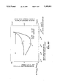
- the minimum dimension at which a punchthrough takes place if a graph is plotted with respect to drain breakdown voltage BVds and a gate length L when the gate is connected to ground, as shown in FIG. 6, and if the gate length L becomes shorter than a certain gate length, BVds starts to decline.
- Such a gate length is set as a minimum dimension L punch at which a punch-through takes place.
- FIGS. 9 and 10 show favorable values with respect to both the deterioration rate of Gm MAX due to hot carriers and the minimum dimension at which a punch-through takes place in accordance with the range of the above-described embodiment.
- This can be considered as follows: The deeper from the substrate surface the maximum concentration of impurities of the n-type layer 106 of low-concentration impurities, the deeper from the substrate surface is the spot at which hot carriers are generated in the vicinity of a drain, so that the rate of deterioration of Gm MAX due to hot carriers becomes small.
- a punch-through is otherwise liable to occur, it is impossible to deepen the maximum concentration location unduly. There is an optimum range for this location.
- the effect of alleviation of an electric field in the vicinity of a drain changes due to the concentration of impurities of the n-type layer 106 of low-concentration impurities, so that the rate of deterioration of Gm MAX also changes.
- the rate of deterioration of Gm MAX due to hot carriers becomes large if this concentration of impurities is too high or too low.
- an optimal range of the location at which the concentration of impurities of the n-type layer 106 of low-concentration impurities becomes maximum can be determined from FIG. 9 to be 0.05 to 0.25 ⁇ m from the surface of the silicon substrate, preferably 0.08 to 0.2 ⁇ m for reducing the deterioration rate of Gm MAX due to hot carriers, and more preferably 0.1 to 0.18 ⁇ m.
- the optimal range of the peak concentration of impurities of the n-type layer 106 of low-concentration impurities can be determined from FIG. 10 to be in the range of 1 ⁇ 10 16 cm -3 to 6 ⁇ 10 18 cm -3 , preferably 2 ⁇ 10 16 cm -3 to 2 ⁇ 10 18 cm -3 for reducing the deterioration rate of Gm MAX due to hot carriers, and more preferably 1 ⁇ 10 17 to 1 ⁇ 10 18 cm -3 .
- FIGS. 7 and 8 show the profile of impurities in the direction of the depth of the n-type layer 106 of low concentration impurities and the p-type impurity layer 104 in this case.
- FIG. 7 shows the profile of impurities where at a depth of 0.15 ⁇ m the concentration of impurities of the n-type layer 106 of low-concentration impurities become maximum and at a depth of 0.55 ⁇ m the concentration of impurities of the p-type impurity layer 104 become maximum.
- FIG. 8 shows the profile of impurities where at a depth of 0.15 ⁇ m the concentration of impurities of the n-type layer 106 of low-concentration impurities become maximum and at a depth of 0.2 ⁇ m the concentration of impurities of the p-type impurity layer 104 become maximum.
- a p-type region having a higher concentration of impurities than that of the silicon substrate is present at a location deeper than the n-type layer 106 of low-concentration impurities.
- both the deterioration rate of Gm MAX due to hot carriers and the minimum dimension at which a punchthrough takes place show favorable values in FIGS. 11 and 12 in the range of the above-described embodiment.
- This can be considered as follows: If a p-type layer 104 having a higher concentration of impurities than that of the silicon substrate 101 is formed at a location deeper than the n-type layer 106 of low-concentration impurities due to the p-type impurity layer 104, the spreading of the drain depletion layer can be held, so that it becomes difficult for a punch-through to take place. However, this does not mean that the location can be set too deep.
- the depth of the p-type impurity layer 104 becomes greater than that of the spreading region of the drain depletion layer, so that it becomes impossible to restrain the spreading of the drain depletion layer, with the adverse result that a punch-through is liable to occur.
- the spot where the avalanche phenomenon occurs in the vicinity of a drain due to a drain electric field is brought to a position deep from the substrate, the deterioration rate of Gm due to hot carriers is lowered. Nevertheless, if the depth of the p-type impurity layer 104 is set lower than a certain position, the spot where the avalanche phenomenon occurs does not change, so that the deterioration rate of Gm MAX is not improved to a remarkable extent.
- the range of the maximum value of the concentration of impurities of the p-type impurity layer 104 can be determined to be in the range of 1 ⁇ 10 16 cm -3 to more preferably 1 ⁇ 10 17 cm -3 to 1 ⁇ 10 18 cm -3 .
- FIG. 13 is a graph illustrating the time dependence of deterioration of Gm due to hot carriers in MOS transistors according to the above-described embodiment of the invention and an example of the prior art, in which A relates to the invention and B relates to the prior art. This diagram reveals that the deterioration rate of Gm in accordance with the invention is approximately 1/5 that of the prior art.
- boron is used as the p-type impurity of the p-type impurity layer 104
- aluminum, gallium, or indium may alternatively be used, or a combination of such impurities, such as boron and aluminum, may be used.
- phosphorous is used as the n-type impurity in the n-type layer 106 of low-concentration impurities, arsenic or antimony may be used, or a combination of such impurities, such as arsenic and phosphorous, may be used.
- a refractory metal such as titanium, molybdenum, or tungsten
- a refractory metal polycide film in which a refractory metal such as titanium, molybdenum, or tungsten or a silicide thereof is formed on a semiconductor film such as a polycrystalline silicon film, or a refractory metal itself or a silicide thereof itself may be used.
- a silicon oxide film formed by the CVD process is used as the side wall insulating film, a silicon oxide film obtained by thermally oxidizing a polycrystalline silicon film may be used, or a silicon nitride film may be used.
- the element isolating region is formed by the LOCOS process
- the trench isolation process in which, after a trench is provided in the semiconductor substrate, the one obtained by embedding the trench with an insulating film such as an oxide film is used as the element isolating region (see FIG. 4).
- the transistor shown in FIG. 1 is used as a transistor constituting a flip-flop of a memory cell of an SRAM, strong protection can be obtained against soft errors caused by d-particles. If d-particles penetrate into the n-type diffusion layer in a drain region of the transistor constituting a flip-flop of an SRAM, pairs of electrons and holes are generated in a depletion layer formed between an n+ diffusion layer and a p-type substrate. The generated electrons are drawn by an electric field in the direction of a drain of the transistor and are injected into the drain diffusion layer.
- the drain diffusion layer is in the high state of the flip-flop, the potential is lowered by the injected electrons, so that the high state turns to the low state. This is the soft error due to d-particles.
- the width of the depletion layer becomes narrow due to the n-type impurity layers 106, 109 and the p-type impurity layer 104.
- MOS transistors can be provided with very short channels up to submicron size, which allows not only high levels of integration and high speed of LSIs to be attained but also the rate of deterioration of characteristics due to hot carriers can be minimized.
- MOS device is used for a memory cell of an SRAM, its protection against soft errors caused by d-particles can be enhanced.
- the present invention plays a large role in improving the reliability of LSIs.
Landscapes
- Insulated Gate Type Field-Effect Transistor (AREA)
Abstract
A semiconductor device composed of: a semiconductor substrate of a first conductivity type having a first impurity concentration; a belt-shaped impurity layer of the first conductivity type which is formed in the substrate so as to be spaced apart from a surface of the substrate and which has a second impurity concentration which is higher than the first concentration at a first depth from the surface of the substrate; a gate electrode formed on the substrate via a first insulating film; a second impurity layer of a second conductive type which is formed in the substrate on both sides of the gate electrode such as to be spaced apart from each other and has a third impurity concentration at a second depth from the surface of the semiconductor substrate, whose lower surface abuts against the first impurity layer or is present thereabove, the second impurity layer having a configuration projecting downward of the gate electrode at a portion thereof adjacent to the first impurity layer; side wall insulating films each formed on a side wall of the gate electrode; and a third impurity layer of the second conductivity type which is formed in the second impurity layer laterally of the side wall insulating film and has a fourth concentration higher than the third concentration.
Description
This is a division of application Ser. No. 07/395,735 filed on Aug. 17, 1989, now U.S. Pat. No. 5,060,033.
The present invention relates to a semiconductor device, and more particularly to the structure of an MOS or MIS semiconductor device and a method of producing the same.
In recent years, the trend toward increasing levels of circuit integration is underway in semiconductor devices. This also applies to MOS transistors, and the circuit dimensions of this type of device have become extremely small, reaching even submicron regions. As such a trend toward smaller circuit dimensions progresses, a phenomenon called punch-through takes place in which a current flows between a source and a drain irrespective of the gate voltage. To solve this problem, a method for increasing the density of impurities in a portion deeper than a substrate surface are known, as disclosed in Japanese Patent Publication No. 16194/1979 and Japanese Patent Laid-Open Applications Nos. 127273/1978, 180167/1985, and 235471/1985. A description will be given of this method with reference to FIG. 2. In FIG. 2, reference numeral 201 denotes a p-type semiconductor substrate, such as a P-type silicon substrate; 202, an element isolating insulation film; 203, a gate insulating film; 209, a source region and a drain region both formed of an n-type layer of high-concentration impurities; 205, a gate electrode; and 204, a p-type layer of impurities having a higher concentration of impurities than the semiconductor substrate 201. Even if the depletion layer of the drain spreads on application of a voltage to the drain, the spreading of the depletion layer is held by the p-type layer of impurities 204, thereby preventing the occurrence of a punch-through.
In addition, if the trend toward smaller circuit dimensions is advanced with a supply voltage fixed, deterioration of characteristics occurs due to hot carriers. To solve this problem, a structure called an LDD (lightly doped drain) was proposed. However, a structure in which further improvements are made on this LDD is disclosed in the following literature 1: Ching-Yeu Wei, J. M. Pimbley, Y. Nissan-Cohen, "Buried and Graded/Buried LDD structures for Improved Hot-Electron Reliability", IEEE Electron Device Lett., Vol. EDL-7, No. 6, pp. 380-382, Jun. 1986. A description of this structure will be given with reference to FIG. 3. In FIG. 3, reference numeral 301 denotes a p-type silicon substrate formed of a p-type semiconductor; 302, an element isolating insulating film formed of an oxide film or the like; 303, a gate insulating film formed of an oxide film or the like; 305, a gate electrode; 309, a source region and a drain region both formed of an n-type layer of high-concentration impurities; 306, a source region and a drain region both formed of an n-type layer of low-concentration impurities; 308, a side wall insulating film; and 304, a p-type layer of impurities having a higher concentration of impurities than the semiconductor substrate 30. The source region and the drain region formed of the n-type layer 306 of low-concentration impurities is deeper than the channel of an MOS-type transistor, and extends inwardly of the gate electrode. As a result, since the passage of a circuit flowing through the channel is bent downward at a drain end, and a spot where hot carriers are generated also moves to the inside of the substrate, it has been known that the frequency at which the generated hot carriers jump into the interface between the gate oxide film and the channel is reduced, thereby minimizing the deterioration rate of the MOS transistor due to hot carriers.
However, since in the conventional example shown in FIG. 2 the concentration of impurities in a portion deeper than the substrate surface is made higher, a punch-through is unlikely to occur, but since no measures have been taken with respect to the concentration of an electric field in the vicinity of a drain, there has been a problem in that the characteristics become deteriorated due to hot carriers.
In addition, although in the conventional example shown in FIG. 3 deterioration of the characteristics due to hot carriers is minimized, there has been a drawback in that since the source region and the drain region project inwardly of the gate electrode, a drain depletion layer and a source depletion layer are liable to be connected to each other, possibly resulting in a punch-through. Furthermore, since the threshold voltage of the MOS transistor is also involved, if the p-type layer 304 having a concentration of impurities higher than that of the semiconductor substrate 301 is formed in the vicinity of the surface of the semiconductor substrate 301, an avalanche phenomenon is liable to occur in the vicinity of the surface, with the adverse result that the deterioration of the MOS transistor becomes great.
Accordingly, an object of the present invention is to provide an MOS transistor which prevents punchthrough even if the circuit dimension thereof becomes very small and the deterioration of characteristics thereof due to hot carriers is minimized, thereby overcoming the above-described drawbacks of the conventional art.
To this end, according to one aspect of the present invention there is provided a semiconductor device comprising: a semiconductor substrate of a first conductivity type having a first concentration; a first belt-shaped impurity layer of the first conductivity type which is formed in the semiconductor substrate such as to be spaced apart from a surface of the semiconductor substrate and which has a second concentration which is higher than that of the first concentration at a first depth from the surface of the semiconductor substrate; a gate electrode formed on the semiconductor substrate via a first insulating film; impurity regions of a second conductivity type which are formed in the semiconductor substrate on both sides of the gate electrode such as to be spaced apart from each other and having a third concentration at a second depth from the surface of the semiconductor substrate, the lower surface of the regions abutting against the first impurity layer or being present thereabove, the impurity regions having a configuration projecting downward of the gate electrode at a portion thereof adjacent to the first impurity layer; side wall insulating films each formed on a side wall of the gate electrode; and a second impurity layer of the second conductivity type which is formed in the impurity regions laterally of the side wall insulating film and having a fourth concentration higher than the third concentration.
According to another aspect of the present invention, there is provided a method of producing a semiconductor device, comprising the steps of: forming a first insulating film on a semiconductor substrate of a first conductivity type; ion-implanting first impurities of the first conductivity type into the semiconductor substrate; forming a gate electrode on the first insulating film; ion-implanting second impurities of a second conductivity type opposite to the first conductive type of the semiconductor substrate into the semiconductor substrate with the gate electrode serving as a mask, in such a manner that a peak of the concentration of the second impurities is lower than a peak of the concentration of the first impurities; forming a side wall insulating film on the gate electrode by means of a second insulating film; and ion-implanting third impurities of the second conductivity type into the semiconductor substrate with the gate electrode and the side wall insulating film serving as masks.
The above and other objects, features and advantages of the present invention will become more apparent from the following detailed description of the invention when read in conjunction with the accompanying drawings.
FIGS. 1(a) to 1(h) are cross-sectional views of stages in a process according to an embodiment of a method of producing a semiconductor device in accordance with the present invention, in which FIG. 1(h) is a schematic cross-sectional view illustrating an embodiment of the semiconductor device in accordance with the present invention.
FIGS. 2 and 3 are schematic cross-sectional views of conventional semiconductor devices.
FIG. 4 is a schematic cross-sectional view illustrating another embodiment of the present invention.
FIG. 5 is a graph explaining GmMAX.
FIG. 6 is a graph explaining Lpunch.
FIGS. 7 and 8 are graphs illustrating a profile of impurities in the direction of the depth of a substrate.
FIGS. 9 to 12 are graphs respectively illustrating deterioration rate of GmMAX due to hot carriers and a minimum dimension Lpunch at which a punch-through takes place.
FIG. 13 is a diagram illustrating the time dependence of deterioration in Gm due to hot carriers of an MOS transistor, in which A relates to an embodiment of the invention, while B relates to a conventional example.
A detailed description will be given of an embodiment of the present invention with reference to FIGS. 1(a) to 1(h). FIG. 1(h) is a cross-sectional view of an MOS transistor in a final process in accordance with the present invention. As shown in FIG. 1(h), the MOS transistor in accordance with the present invention comprises a semiconductor substrate 101, e.g., a p-type silicon substrate; an element isolating separating insulation film 102, e.g., a silicon oxide film; an insulating film 103, such as a gate insulating film constituted by a silicon oxide film; a p-type layer 104 having an impurity concentration higher than that of silicon substrate 101; a gate electrode 105; source and drain regions 106 formed by an n-type layer of low-concentration impurities; a side wall insulating film 108 formed from a silicon oxide film 107 or the like; and source and drain regions 109 formed by an n-type layer of high-concentration impurities. The mark--indicates the location in layer 104 at which the concentration of impurities of the p-type layer of concentration impurities becomes maximum. The mark X indicates the locations where the concentration of impurities of the n-type regions 106 of low-concentration impurities becomes maximum.
First, as shown in FIG. 1(a), a semiconductor substrate of a first conductivity type, i.e., the p-type silicon substrate 101 in this case, is subjected to oxidation at 1,000° C. in an oxidizing atmosphere so as to form a silicon oxide film with a 500 Å thickness. Subsequently, a silicon nitride film with a thickness of 2000 Å is formed by the CVD process. Then, after unnecessary portions of the silicon nitride film are removed by a photoetching process, the silicon substrate 101 is subjected to oxidation at 1,000° C. in a wet atmosphere to form an element isolating insulation film 103 constituted by an oxide film with an approximate 1 μm thickness, and the aforementioned silicon nitride film is then removed. Through these processes, the silicon oxide film which serves as the element isolating insulation film 102 is formed on the p-type silicon substrate 101, as shown in FIG. 1(a).
Subsequently, as shown in FIG. 1(b), the p-type silicon substrate 101 is subjected to oxidation at 1,000° C. in an oxidizing atmosphere, and a gate insulating film 103 constituted by an oxide film with a 200 Å thickness is formed on the p-type silicon substrate 101.
Then, as shown in FIG. 1(c), p-type impurities, e.g., boron, are ion-implanted at a dosage of 1×1012 cm-2 to 1×1014 cm-2 and at an acceleration voltage of 60 KeV to 200 KeV to form the p-type layer 104 having an impurity concentration higher than that of the silicon substrate.
Then, as shown in FIG. 1(d), after a polycrystalline silicon film having a 6,000 Å is formed by the CVD process, unnecessary portions of that film are removed by a photoetching process so as to form the gate electrode 105.
Subsequently, as shown in FIG. 1(e), n-type impurities, e.g., phosphorous are ion-implanted at a dosage of 1×1012 cm-2 to 1×1014 cm-2 and at an acceleration voltage of 80 KeV to 180 KeV with the gate electrode 105 and the element isolating insulation film 102, constituted by the silicon oxide film, serving as masks so as to form the n-type layer 106 of low-concentration impurities for the source and drain regions.
Then, as shown in FIG. 1(f), after the silicon oxide film 107 with a 6000 Å thickness is formed on the semiconductor substrate 101 and the gate electrode 105 by means of the CVD process, reactive ion-etching is performed so as to form the side wall insulating film 108 from the silicon oxide film, as shown in FIG. 1(g).
Subsequently, as shown in FIG. 1(h), n-type impurities, e.g., arsenic, are ion-implanted at a dosage of 1×1012 cm-2 and at an acceleration voltage of 80 KeV with the gate electrode 105, the side wall insulating film 108, and the element isolating insulation film 102 serving as masks so as to form the n-type layer, or regions, 109 of high-concentration impurities for the source and drain regions.
Finally, to activate the ion-implanted layers, the MOS transistor is subjected to annealing at 800° C. to 1100° C. In the case of the MOS transistor thus formed, if the concentration of the p-type impurities of the p-type silicon substrate 101, i.e., the concentration of impurities of boron in this case, is set to 5×1015 cm-3, the maximum value of the concentration of impurities of the n-type layer 106 of low-concentration impurities becomes 1×1016 cm-3 to 6×1018 cm-3, and a location at which the value becomes maximum is 0.05 to 0.25 μm deep from the surface of the silicon substrate, so that the n-type layer 106 of low-concentration impurities projects 0.05 to 0.15 μm inwardly of, or under, the gate electrode 105.
In each of FIGS. 5, 9, 10, 11 and 12, to be described in detail below, there are two curves and two ordinate scales. Each curve is associated with an arrow pointing to its corresponding ordinate scale.
The curves of FIGS. 9, 10, 11, 12 and 13 were all made with a gate voltage, VG, of +3V and a drain voltage, VD, OF +8V relative to the substrate.
FIG. 9 is a graph illustrating the depth of the location at which the concentration of impurities of the n-type layer 106 of low-concentration impurities becomes maximum, the deterioration rate of Gm due to hot carriers, and the minimum dimension at which a punch-through takes place. FIG. 10 is a graph illustrating the maximum value of the concentration of the n-type layer 106 of low-concentration impurities, the deterioration rate of GMAX due to hot carriers, and the minimum dimension at which a punch-through takes place. As for GmMAX referred to herein, the value of Gm is obtained by differentiating ID with VG in the graph of gate voltage VG and drain current ID of the MOS transistor, as shown in FIG. 5, and the maximum value of Gm is set as GmMAX. In addition, as for the minimum dimension at which a punchthrough takes place, if a graph is plotted with respect to drain breakdown voltage BVds and a gate length L when the gate is connected to ground, as shown in FIG. 6, and if the gate length L becomes shorter than a certain gate length, BVds starts to decline. Such a gate length is set as a minimum dimension Lpunch at which a punch-through takes place.
Both FIGS. 9 and 10 show favorable values with respect to both the deterioration rate of GmMAX due to hot carriers and the minimum dimension at which a punch-through takes place in accordance with the range of the above-described embodiment. This can be considered as follows: The deeper from the substrate surface the maximum concentration of impurities of the n-type layer 106 of low-concentration impurities, the deeper from the substrate surface is the spot at which hot carriers are generated in the vicinity of a drain, so that the rate of deterioration of GmMAX due to hot carriers becomes small. However, since a punch-through is otherwise liable to occur, it is impossible to deepen the maximum concentration location unduly. There is an optimum range for this location.
Furthermore, the effect of alleviation of an electric field in the vicinity of a drain changes due to the concentration of impurities of the n-type layer 106 of low-concentration impurities, so that the rate of deterioration of GmMAX also changes. In other words, the rate of deterioration of GmMAX due to hot carriers becomes large if this concentration of impurities is too high or too low.
In addition, since the tendency of occurrence of a punch-through also changes due to this concentration of impurities, there is an optimum range. If it is assumed that the deterioration rate of GmMAX due to hot carriers is 8% or less and the minimum dimension at which a punch-through takes place is 0.8 μm, an optimal range of the location at which the concentration of impurities of the n-type layer 106 of low-concentration impurities becomes maximum can be determined from FIG. 9 to be 0.05 to 0.25 μm from the surface of the silicon substrate, preferably 0.08 to 0.2 μm for reducing the deterioration rate of GmMAX due to hot carriers, and more preferably 0.1 to 0.18 μm.
In addition, if it is assumed that the deterioration rate of GmMAX due to hot carriers is 8% or below and the minimum dimension at which a punch-through takes place is 0.8 μm, the optimal range of the peak concentration of impurities of the n-type layer 106 of low-concentration impurities can be determined from FIG. 10 to be in the range of 1×1016 cm-3 to 6×1018 cm-3, preferably 2×1016 cm-3 to 2×1018 cm-3 for reducing the deterioration rate of GmMAX due to hot carriers, and more preferably 1×10¹⁷ to 1×1018 cm-3.
In accordance with the above-described embodiment, the location at which the concentration of impurities of p-type impurity layer 104 having a concentration higher than that of the silicon substrate becomes a maximum at a depth of 0.2 μm to 0.55 μm. FIGS. 7 and 8 show the profile of impurities in the direction of the depth of the n-type layer 106 of low concentration impurities and the p-type impurity layer 104 in this case. FIG. 7 shows the profile of impurities where at a depth of 0.15 μm the concentration of impurities of the n-type layer 106 of low-concentration impurities become maximum and at a depth of 0.55 μm the concentration of impurities of the p-type impurity layer 104 become maximum. Meanwhile, FIG. 8 shows the profile of impurities where at a depth of 0.15 μm the concentration of impurities of the n-type layer 106 of low-concentration impurities become maximum and at a depth of 0.2 μm the concentration of impurities of the p-type impurity layer 104 become maximum. As can be seen from FIGS. 7 and 8, looking at the overall concentration of impurities in which n-type impurities and p-type impurities are offset with each other, a p-type region having a higher concentration of impurities than that of the silicon substrate is present at a location deeper than the n-type layer 106 of low-concentration impurities. In this case, both the deterioration rate of GmMAX due to hot carriers and the minimum dimension at which a punchthrough takes place show favorable values in FIGS. 11 and 12 in the range of the above-described embodiment. This can be considered as follows: If a p-type layer 104 having a higher concentration of impurities than that of the silicon substrate 101 is formed at a location deeper than the n-type layer 106 of low-concentration impurities due to the p-type impurity layer 104, the spreading of the drain depletion layer can be held, so that it becomes difficult for a punch-through to take place. However, this does not mean that the location can be set too deep. If the location of the p-type impurity layer 104 is set too deep, the depth of the p-type impurity layer 104 becomes greater than that of the spreading region of the drain depletion layer, so that it becomes impossible to restrain the spreading of the drain depletion layer, with the adverse result that a punch-through is liable to occur.
In addition, since the location at which the concentration of impurities of the p-type impurity layer 104 becomes maximum is set deep, the spot where the avalanche phenomenon occurs in the vicinity of a drain due to a drain electric field is brought to a position deep from the substrate, the deterioration rate of Gm due to hot carriers is lowered. Nevertheless, if the depth of the p-type impurity layer 104 is set lower than a certain position, the spot where the avalanche phenomenon occurs does not change, so that the deterioration rate of GmMAX is not improved to a remarkable extent.
From the foregoing description, it can be seen that an optimal range exists with respect to the location where the concentration of impurities of the p-type impurity layer 104 becomes maximum. If it is assumed that the deterioration rate of GmMAX due to hot carriers is 8% or less and that the minimum dimension at which a punch-through takes place is 0.8 μm, that range can be determined from FIG. 11 as being in the range of 0.2 μm to 0.7 μm from the surface of the silicon substrate, preferably 0.25 μm to 0.55 μm, and more preferably 0.3 μm to 0.5 μm from the surface where hot carriers and the punch-through takes place. In addition, FIG. 12 is a graph illustrating the maximum value of the concentration of impurities in the p-type impurity layer 104, the deterioration rate of GmMAX due to hot carriers, and the minimum dimension at which a punch-through takes place. From this graph, the range of the maximum value of the concentration of impurities of the p-type impurity layer 104 can be determined to be in the range of 1×1016 cm-3 to more preferably 1×1017 cm-3 to 1×1018 cm-3.
FIG. 13 is a graph illustrating the time dependence of deterioration of Gm due to hot carriers in MOS transistors according to the above-described embodiment of the invention and an example of the prior art, in which A relates to the invention and B relates to the prior art. This diagram reveals that the deterioration rate of Gm in accordance with the invention is approximately 1/5 that of the prior art.
Although in this embodiment, boron is used as the p-type impurity of the p-type impurity layer 104, aluminum, gallium, or indium may alternatively be used, or a combination of such impurities, such as boron and aluminum, may be used. In addition, although phosphorous is used as the n-type impurity in the n-type layer 106 of low-concentration impurities, arsenic or antimony may be used, or a combination of such impurities, such as arsenic and phosphorous, may be used.
In addition, although in this embodiment a polycrystalline silicon film is used for the gate electrode, a refractory metal such as titanium, molybdenum, or tungsten may be used, or a refractory metal polycide film in which a refractory metal such as titanium, molybdenum, or tungsten or a silicide thereof is formed on a semiconductor film such as a polycrystalline silicon film, or a refractory metal itself or a silicide thereof itself may be used. Furthermore, although in this embodiment a silicon oxide film formed by the CVD process is used as the side wall insulating film, a silicon oxide film obtained by thermally oxidizing a polycrystalline silicon film may be used, or a silicon nitride film may be used. Moreover, although in this embodiment the element isolating region is formed by the LOCOS process, it is possible to use the trench isolation process in which, after a trench is provided in the semiconductor substrate, the one obtained by embedding the trench with an insulating film such as an oxide film is used as the element isolating region (see FIG. 4).
In this embodiment, if the transistor shown in FIG. 1 is used as a transistor constituting a flip-flop of a memory cell of an SRAM, strong protection can be obtained against soft errors caused by d-particles. If d-particles penetrate into the n-type diffusion layer in a drain region of the transistor constituting a flip-flop of an SRAM, pairs of electrons and holes are generated in a depletion layer formed between an n+ diffusion layer and a p-type substrate. The generated electrons are drawn by an electric field in the direction of a drain of the transistor and are injected into the drain diffusion layer. At this time, if the drain diffusion layer is in the high state of the flip-flop, the potential is lowered by the injected electrons, so that the high state turns to the low state. This is the soft error due to d-particles. However, in the embodiment shown in FIG. 1(h), even if the drain diffusion layer is in the high state, the width of the depletion layer becomes narrow due to the n-type impurity layers 106, 109 and the p-type impurity layer 104. In this case, even if d-particles penetrate into the n-type diffusion layer in the drain region, since the width of the aforementioned depletion layer is made narrow, the number of pairs of electrons and holes generated in the depletion layer becomes small, so that strong protection against soft errors caused by d-particles can be obtained.
Although the embodiment described is an n-channel transistor, it goes without saying that a similar effect can be obtained if the present invention is applied to a p-channel transistor.
In accordance with the present invention, since a punch-through phenomenon is unlikely to occur, MOS transistors can be provided with very short channels up to submicron size, which allows not only high levels of integration and high speed of LSIs to be attained but also the rate of deterioration of characteristics due to hot carriers can be minimized. In addition, if the MOS device is used for a memory cell of an SRAM, its protection against soft errors caused by d-particles can be enhanced. Hence, there is an advantage in that the present invention plays a large role in improving the reliability of LSIs.
While the description above refers to particular embodiments of the present invention, it will be understood that many modifications may be made without departing from the spirit thereof. The accompanying claims are intended to cover such modifications as would fall within the true scope and spirit of the present invention.
The presently disclosed embodiments are therefore to be considered in all respects as illustrative and not restrictive, the scope of the invention being indicated by the appended claims, rather than the foregoing description, and all changes which come within the meaning and range of equivalency of the claims are therefore intended to be embraced therein.
Claims (14)
1. A method of producing a semiconductor device comprising the steps of:
forming a first insulating film on a surface of a semiconductor substrate of a first conductivity type;
ion-implanting first impurities of said first conductivity type into said semiconductor substrate to create a first impurity concentration having a peak;
forming a gate electrode on said first insulating film;
ion-implanting second impurities of a second conductivity type opposite to said first conductivity type of said semiconductor substrate into said semiconductor substrate to create a second impurity concentration having a peak, with said gate electrode serving as a mask, in such a manner that the peak of the concentration of said second impurities is at a shallower depth than the peak of the concentration of said first impurities;
forming a side wall insulating film on said gate electrode; and
ion-implanting third impurities of said second conductivity type into said semiconductor substrate with said gate electrode and said side wall insulating film serving as masks.
2. A method of producing a semiconductor device according to claim 1 wherein said side wall insulating film is formed by depositing a second insulating film on said semiconductor substrate and said gate electrode; and anisotropically ion-etching the second insulating film.
3. A method of producing a semiconductor device according to claim 2 wherein the first impurity concentration peak is at a depth from the surface of the semiconductor substrate of 0.2 to 0.7 μm.
4. A method producing a semiconductor device according to claim 3 wherein the peak concentration of said first impurities in said semiconductor substrate is in the range of 1×10¹⁶ to 3×1018 cm-3.
5. A method of producing a semiconductor device according to claim 1 wherein the first impurity concentration peak is at a depth from the surface of the semiconductor substrate of 0.2 to 0.7 μm.
6. A method producing a semiconductor device according to claim 5 wherein the peak concentration of said first impurities in said semiconductor substrate is in the range of 1×10¹⁶ to 3×1018 cm-3.
7. A method producing a semiconductor device according to claim 2 wherein the peak concentration of said first impurities in said semiconductor substrate is in the range of 1×10¹⁶ to 3×1018 cm-3.
8. A method producing a semiconductor device according to claim 1 wherein the peak concentration of said first impurities in said semiconductor substrate is in the range of 1×10¹⁶ to 3×1018 cm-3.
9. A method of producing a semiconductor device according to claim 8 wherein the second impurity concentration peak is at a depth from the surface of said semiconductor substrate of 0.05 to 0.25 μm.
10. A method of producing a semiconductor device according to claim 9 wherein the peak concentration of said second impurities in said semiconductor substrate is in the range of 1×10¹⁶ to 6×1018 cm-3.
11. A method of producing a semiconductor device according to claim 2 wherein the second impurity concentration peak is at a depth from the surface of said semiconductor substrate of 0.05 to 0.25 μm.
12. A method of producing a semiconductor device according to claim 11 wherein the peak concentration of said second impurities in said semiconductor substrate is in the range of 1×10¹⁶ to 6×1018 cm-3.
13. A method of producing a semiconductor device according to claim 1 wherein the second impurity concentration peak is at a depth from the surface of said semiconductor substrate of 0.05 to 0.25 μm.
14. A method of producing a semiconductor device according to claim 1 wherein the peak concentration of said second impurities in said semiconductor substrate is in the range of 1×10¹⁶ to 6×1018 cm-3.
Priority Applications (1)
| Application Number | Priority Date | Filing Date | Title |
|---|---|---|---|
| US07/707,160 US5180682A (en) | 1988-08-18 | 1991-05-28 | Semiconductor device and method of producing semiconductor device |
Applications Claiming Priority (4)
| Application Number | Priority Date | Filing Date | Title |
|---|---|---|---|
| JP63205535A JPH0254537A (en) | 1988-08-18 | 1988-08-18 | Semiconductor device and semiconductor device manufacturing method |
| JP63-205535 | 1988-08-18 | ||
| US07/395,735 US5060033A (en) | 1988-08-18 | 1989-08-17 | Semiconductor device and method of producing semiconductor device |
| US07/707,160 US5180682A (en) | 1988-08-18 | 1991-05-28 | Semiconductor device and method of producing semiconductor device |
Related Parent Applications (1)
| Application Number | Title | Priority Date | Filing Date |
|---|---|---|---|
| US07/395,735 Division US5060033A (en) | 1988-08-18 | 1989-08-17 | Semiconductor device and method of producing semiconductor device |
Publications (1)
| Publication Number | Publication Date |
|---|---|
| US5180682A true US5180682A (en) | 1993-01-19 |
Family
ID=27328512
Family Applications (1)
| Application Number | Title | Priority Date | Filing Date |
|---|---|---|---|
| US07/707,160 Expired - Lifetime US5180682A (en) | 1988-08-18 | 1991-05-28 | Semiconductor device and method of producing semiconductor device |
Country Status (1)
| Country | Link |
|---|---|
| US (1) | US5180682A (en) |
Cited By (3)
| Publication number | Priority date | Publication date | Assignee | Title |
|---|---|---|---|---|
| US5589410A (en) * | 1992-01-07 | 1996-12-31 | Fujitsu Limited | An integrated semiconductor device having a buried semiconductor layer and fabrication method thereof |
| US5635413A (en) * | 1992-08-03 | 1997-06-03 | Mitsubishi Denki Kabushiki Kaisha | Method of manufacturing field effect transistor |
| US20070212861A1 (en) * | 2006-03-07 | 2007-09-13 | International Business Machines Corporation | Laser surface annealing of antimony doped amorphized semiconductor region |
Citations (7)
| Publication number | Priority date | Publication date | Assignee | Title |
|---|---|---|---|---|
| US4577391A (en) * | 1984-07-27 | 1986-03-25 | Monolithic Memories, Inc. | Method of manufacturing CMOS devices |
| US4642878A (en) * | 1984-08-28 | 1987-02-17 | Kabushiki Kaisha Toshiba | Method of making MOS device by sequentially depositing an oxidizable layer and a masking second layer over gated device regions |
| US4818714A (en) * | 1987-12-02 | 1989-04-04 | Advanced Micro Devices, Inc. | Method of making a high performance MOS device having LDD regions with graded junctions |
| US4851257A (en) * | 1987-03-13 | 1989-07-25 | Harris Corporation | Process for the fabrication of a vertical contact |
| US4906588A (en) * | 1988-06-23 | 1990-03-06 | Dallas Semiconductor Corporation | Enclosed buried channel transistor |
| US4943537A (en) * | 1988-06-23 | 1990-07-24 | Dallas Semiconductor Corporation | CMOS integrated circuit with reduced susceptibility to PMOS punchthrough |
| US5024960A (en) * | 1987-06-16 | 1991-06-18 | Texas Instruments Incorporated | Dual LDD submicron CMOS process for making low and high voltage transistors with common gate |
-
1991
- 1991-05-28 US US07/707,160 patent/US5180682A/en not_active Expired - Lifetime
Patent Citations (7)
| Publication number | Priority date | Publication date | Assignee | Title |
|---|---|---|---|---|
| US4577391A (en) * | 1984-07-27 | 1986-03-25 | Monolithic Memories, Inc. | Method of manufacturing CMOS devices |
| US4642878A (en) * | 1984-08-28 | 1987-02-17 | Kabushiki Kaisha Toshiba | Method of making MOS device by sequentially depositing an oxidizable layer and a masking second layer over gated device regions |
| US4851257A (en) * | 1987-03-13 | 1989-07-25 | Harris Corporation | Process for the fabrication of a vertical contact |
| US5024960A (en) * | 1987-06-16 | 1991-06-18 | Texas Instruments Incorporated | Dual LDD submicron CMOS process for making low and high voltage transistors with common gate |
| US4818714A (en) * | 1987-12-02 | 1989-04-04 | Advanced Micro Devices, Inc. | Method of making a high performance MOS device having LDD regions with graded junctions |
| US4906588A (en) * | 1988-06-23 | 1990-03-06 | Dallas Semiconductor Corporation | Enclosed buried channel transistor |
| US4943537A (en) * | 1988-06-23 | 1990-07-24 | Dallas Semiconductor Corporation | CMOS integrated circuit with reduced susceptibility to PMOS punchthrough |
Cited By (3)
| Publication number | Priority date | Publication date | Assignee | Title |
|---|---|---|---|---|
| US5589410A (en) * | 1992-01-07 | 1996-12-31 | Fujitsu Limited | An integrated semiconductor device having a buried semiconductor layer and fabrication method thereof |
| US5635413A (en) * | 1992-08-03 | 1997-06-03 | Mitsubishi Denki Kabushiki Kaisha | Method of manufacturing field effect transistor |
| US20070212861A1 (en) * | 2006-03-07 | 2007-09-13 | International Business Machines Corporation | Laser surface annealing of antimony doped amorphized semiconductor region |
Similar Documents
| Publication | Publication Date | Title |
|---|---|---|
| US7064399B2 (en) | Advanced CMOS using super steep retrograde wells | |
| JP3094293B2 (en) | Method for manufacturing semiconductor device | |
| US6255152B1 (en) | Method of fabricating CMOS using Si-B layer to form source/drain extension junction | |
| US5548143A (en) | Metal oxide semiconductor transistor and a method for manufacturing the same | |
| US5362982A (en) | Insulated gate FET with a particular LDD structure | |
| US4924277A (en) | MIS transistor device | |
| US5060033A (en) | Semiconductor device and method of producing semiconductor device | |
| WO1997023000A1 (en) | SEMICONDUCTOR FIELD EFFECT DEVICE COMPRISING A SiGe LAYER | |
| JPH06342884A (en) | MOS semiconductor device and manufacturing method thereof | |
| JP3394408B2 (en) | Semiconductor device and manufacturing method thereof | |
| US6767778B2 (en) | Low dose super deep source/drain implant | |
| US7087961B2 (en) | Semiconductor device with reduced on-state resistance | |
| US6204543B1 (en) | Semiconductor device having LDD structure and method for producing the same | |
| US20050164439A1 (en) | Low volt/high volt transistor | |
| US5973370A (en) | Preventing boron penetration through thin gate oxide of P-channel devices in advanced CMOS technology | |
| US5504024A (en) | Method for fabricating MOS transistors | |
| US6476430B1 (en) | Integrated circuit | |
| US6885066B2 (en) | SOI type MOSFET | |
| US5180682A (en) | Semiconductor device and method of producing semiconductor device | |
| JP2578662B2 (en) | Method for manufacturing semiconductor device | |
| US6727149B1 (en) | Method of making a hybrid SOI device that suppresses floating body effects | |
| KR100463044B1 (en) | Method of manufacturing semiconductor device | |
| US6541341B1 (en) | Method for fabricating MOS field effect transistor | |
| JP2591518B2 (en) | Semiconductor device | |
| KR100269280B1 (en) | LDD type transistors manufacturing method |
Legal Events
| Date | Code | Title | Description |
|---|---|---|---|
| STCF | Information on status: patent grant |
Free format text: PATENTED CASE |
|
| FEPP | Fee payment procedure |
Free format text: PAYOR NUMBER ASSIGNED (ORIGINAL EVENT CODE: ASPN); ENTITY STATUS OF PATENT OWNER: LARGE ENTITY |
|
| FPAY | Fee payment |
Year of fee payment: 4 |
|
| FPAY | Fee payment |
Year of fee payment: 8 |
|
| FPAY | Fee payment |
Year of fee payment: 12 |