US5166772A - Transfer molded semiconductor device package with integral shield - Google Patents
Transfer molded semiconductor device package with integral shield Download PDFInfo
- Publication number
- US5166772A US5166772A US07/658,810 US65881091A US5166772A US 5166772 A US5166772 A US 5166772A US 65881091 A US65881091 A US 65881091A US 5166772 A US5166772 A US 5166772A
- Authority
- US
- United States
- Prior art keywords
- semiconductor device
- metallization pattern
- device package
- metal screen
- shield
- Prior art date
- Legal status (The legal status is an assumption and is not a legal conclusion. Google has not performed a legal analysis and makes no representation as to the accuracy of the status listed.)
- Expired - Fee Related
Links
Images


Classifications
-
- H10W74/114—
-
- H10W42/20—
-
- H10W42/60—
-
- H10W72/5445—
-
- H10W72/884—
-
- H10W72/932—
-
- H10W74/00—
-
- H10W90/734—
-
- H10W90/754—
Definitions
- This invention relates generally to semiconductor device packages and more specifically to radio frequency shielded semiconductor device packages.
- thermoset or thermoplastic resin This package provides protection from dust, humidity and other environmental factors which can destroy the delicate circuitry.
- shielding systems are generally characterized by a conductive metallic enclosure constructed to surround the device to be shielded. This enclosure acts either to protect the electrical equipment from external RFI or EMI signals or to prevent the escape of RFI or EMI signals generated by the device.
- these shielded enclosures are made from a conductive material that is electrically coupled to the surrounding area.
- the shielded enclosures have been made by attaching a drawn metallic casing over the transfer molded package and soldering the metal casing to a substrate connected to the device.
- Heat generated by the soldering process may be conducted directly to the integrated circuit and can result in damage to the circuit.
- due care is required to control the soldering process in order to prevent jeopardizing the quality of the integrated circuit.
- the increase in the overall size of the shielded package is substantial, due to the additional thickness of the shield. This thickness results in a package that is larger than optimum.
- the step of soldering the shield also requires additional assembly time and labor, adding further cost to the final package. Providing shielding for integrated circuits in this way requires special mounting and holding fixtures for the shield and the integrated circuit package.
- the semiconductor device package comprises a substrate having a metallization pattern, with one portion of the metallization pattern being a circuit ground.
- a semiconductor device is electrically interconnected to a first side of the metallization pattern.
- a perforated metal shield or screen covers the semiconductor device and is electrically and mechanically attached to the metallization circuit ground in order to shield the semiconductor device from radio frequency energy.
- a resin material is transfer molded about the semiconductor device, the electrical interconnections, and the metal screen to form the completed package.
- the method of manufacturing the semiconductor device package comprises the steps of:
- Providing a substrate comprising a sheet of material having a metallization pattern on at least one side;
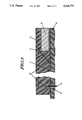
- FIG. 1 is an isometric cut-away view of the shielded semiconductor device package in accordance with the present invention.
- FIG. 2 is a cross-sectional view of the shielded semiconductor device package through section 2--2 of FIG. 1.
- FIG. 3 is a pictorial sequence of the steps involved in manufacturing the shielded semiconductor device package.
- a substrate 10 is provided as a carrier, with a metallization pattern.
- the substrate material may be any one of a number of materials commonly used in the industry, such as polyester, polyimide, polyetherimide, polytetrafluoroethylene, glass reinforced printed circuit board materials, metal, ceramics, or glass, and may be rigid or flexible.
- Substrate thickness may vary from approximately 0.001 inches to 0.250 inches, with thicknesses ranging from 0.005 to 0.075 being preferred.
- the metallization pattern consists of a conventional die mounting pad (not shown) with wire bond pads 12 arranged around the periphery of the die mount pad.
- a semiconductor device 16 is mechanically attached to the metallization pattern by means of a conductive adhesive or solder to bond the semiconductor device 16 to the die mounting pad. Nonconductive adhesives may also be utilized if electrical conductivity between the semiconductor device and the die mounting pad is not required.
- the semiconductor device 16 is then connected to the wire bond pads 12 by wirebonds 17.
- Other means of connecting semiconductor device 16 to the circuit pattern such as flip-chip bonding or tape-automated bonding (TAB) may be used interchangeably and still fall within the scope of the invention. These attachment methods are common in the industry and are well known to those skilled in the art.
- the EMI/RFI shield 18 is added to the package by placing the shield 18 over the semiconductor device 16 and the associated wirebonds 17 and electrical interconnections.
- the shield 18 may be a metal screen made from copper, nickel, chrome, stainless steel or other alloys, and may be plated with other metals to enhance corrosion resistance, improve solderability, or add to electrical shielding efficiency for example, with gold, tin, lead, indium, palladium, platinum, and alloys of these or other metals.
- Other form factors for the shield include a perforated metal sheet preformed into the desired shape.
- the prime requirements for the shield material are that it be conductive, be able to be electrically connected to the circuit ground, and have openings that will permit the transfer molding compounds 14 to pass through the shield 18 to the semiconductor device 16 without unduly restricting the flow of the transfer molding compound 14 during the molding operation.
- the shield 18 is connected to the ground circuit by forming portions of the shield into legs 19.
- the legs 19 are connected to the circuit metallization pattern by placing the legs 19 into plated through holes 13 or onto surface mount pads (not shown) of the substrate 10.
- the legs 19 of the screen 18 are electrically attached to the substrate preferably by use of a conductive adhesive or alternatively by a simple mechanical pressure contact between the legs and a surface mount pad or by reflowing a solder ball or solder paste onto the pad or hole. The electrical attachment may be made prior to the transfer molding operation or after the molding operation.
- the assembly is now encapsulated by placing it into a transfer molding cavity, and transfer molding a thermoplastic or thermoset material about the assembly.
- the molding compound 14 flows through the openings in the metal shield 18 and encapsulates the semiconductor device 16 the same as if the shield 18 were not present.
- the transfer molding compound 14 is on both sides of the metal shield, however the package may be formed such that there is no molding material on the exterior side of the shield, thereby exposing one side of the shield.
- the perforations or openings in the metal shield serve to allow the molding compound easy passage through the shield in order to form a solid monolithic package.
- a substrate 10 is formed to include a metallization pattern with wire bond pads 12.
- a semiconductor device 16 is mechanically attached to the substrate 10 and electrically attached to the substrate by means of wire bonds 17, or by flip chip or TAB attachment techniques.
- the shield 18 is placed over the semiconductor device and associated wirebonds.
- the shield 18 may consist of a wire mesh of a perforated metal sheet, and may be preformed into the desired shape or formed in place.
- the edges 19 of the metal shield are connected to the substrate circuit ground by bonding with a conductive adhesive to the circuit ground. In some cases, portions of the shield may be formed into legs and inserted into plated holes 13 in the substrate, but plated holes are not a requirement.
- the substrate and semiconductor device assembly is encapsulated by transfer molding with a thermoplastic or thermoset transfer molding compound 14 to form a solid mass.
- the transfer molding compound 14 totally encapsulates the semiconductor device 16, the associated wirebonds 17, the metal shield 18, and portions of the metallization pattern and substrate.
- the overall package height is only slightly increased by the shield.
- the size and cost of the package is reduced when compared to the prior art, and significantly reduced in those cases where complex shields are required.
- the method of producing semiconductor packages as elucidated in the present invention clearly realizes a number of advantages over the existing prior art by creating a package that is particularly useful in high density electronic applications, such as radios devices.
- the small size of the package, coupled with the improved shielding capability allow this package to be advantageously employed in applications such as portable radio transmitters, portable telephones, or portable radio receivers.
- FIGS. 1-3 While illustrative, are not meant to be considered limiting and other configurations and shapes of the semiconductor package may be envisioned to fall within the scope of the invention.
Landscapes
- Shielding Devices Or Components To Electric Or Magnetic Fields (AREA)
- Structures Or Materials For Encapsulating Or Coating Semiconductor Devices Or Solid State Devices (AREA)
Abstract
Description
Claims (10)
Priority Applications (1)
| Application Number | Priority Date | Filing Date | Title |
|---|---|---|---|
| US07/658,810 US5166772A (en) | 1991-02-22 | 1991-02-22 | Transfer molded semiconductor device package with integral shield |
Applications Claiming Priority (1)
| Application Number | Priority Date | Filing Date | Title |
|---|---|---|---|
| US07/658,810 US5166772A (en) | 1991-02-22 | 1991-02-22 | Transfer molded semiconductor device package with integral shield |
Publications (1)
| Publication Number | Publication Date |
|---|---|
| US5166772A true US5166772A (en) | 1992-11-24 |
Family
ID=24642801
Family Applications (1)
| Application Number | Title | Priority Date | Filing Date |
|---|---|---|---|
| US07/658,810 Expired - Fee Related US5166772A (en) | 1991-02-22 | 1991-02-22 | Transfer molded semiconductor device package with integral shield |
Country Status (1)
| Country | Link |
|---|---|
| US (1) | US5166772A (en) |
Cited By (175)
| Publication number | Priority date | Publication date | Assignee | Title |
|---|---|---|---|---|
| US5309321A (en) * | 1992-09-22 | 1994-05-03 | Microelectronics And Computer Technology Corporation | Thermally conductive screen mesh for encapsulated integrated circuit packages |
| US5326932A (en) * | 1992-01-14 | 1994-07-05 | Goldstar Electron Co., Ltd. | Semiconductor package |
| WO1994018707A1 (en) * | 1993-02-04 | 1994-08-18 | Motorola, Inc. | Thermally conductive integrated circuit package with radio frequency shielding |
| US5353195A (en) * | 1993-07-09 | 1994-10-04 | General Electric Company | Integral power and ground structure for multi-chip modules |
| US5355016A (en) * | 1993-05-03 | 1994-10-11 | Motorola, Inc. | Shielded EPROM package |
| US5399902A (en) * | 1993-03-04 | 1995-03-21 | International Business Machines Corporation | Semiconductor chip packaging structure including a ground plane |
| US5406117A (en) * | 1993-12-09 | 1995-04-11 | Dlugokecki; Joseph J. | Radiation shielding for integrated circuit devices using reconstructed plastic packages |
| US5436203A (en) * | 1994-07-05 | 1995-07-25 | Motorola, Inc. | Shielded liquid encapsulated semiconductor device and method for making the same |
| US5455456A (en) * | 1993-09-15 | 1995-10-03 | Lsi Logic Corporation | Integrated circuit package lid |
| US5471088A (en) * | 1992-11-07 | 1995-11-28 | Goldstar Electron Co., Ltd. | Semiconductor package and method for manufacturing the same |
| US5473112A (en) * | 1993-09-13 | 1995-12-05 | Vlsi Technology, Inc. | Security circuitry with select line and data line shielding |
| US5525834A (en) * | 1994-10-17 | 1996-06-11 | W. L. Gore & Associates, Inc. | Integrated circuit package |
| US5530202A (en) * | 1995-01-09 | 1996-06-25 | At&T Corp. | Metallic RF or thermal shield for automatic vacuum placement |
| US5561265A (en) * | 1993-03-24 | 1996-10-01 | Northern Telecom Limited | Integrated circuit packaging |
| US5639989A (en) * | 1994-04-19 | 1997-06-17 | Motorola Inc. | Shielded electronic component assembly and method for making the same |
| US5668406A (en) * | 1994-05-31 | 1997-09-16 | Nec Corporation | Semiconductor device having shielding structure made of electrically conductive paste |
| US5701032A (en) * | 1994-10-17 | 1997-12-23 | W. L. Gore & Associates, Inc. | Integrated circuit package |
| US5744869A (en) * | 1995-12-05 | 1998-04-28 | Motorola, Inc. | Apparatus for mounting a flip-chip semiconductor device |
| US5761054A (en) * | 1995-03-28 | 1998-06-02 | Intel Corporation | Integrated circuit assembly preventing intrusions into electronic circuitry |
| EP0853340A3 (en) * | 1993-12-29 | 1998-08-05 | Nec Corporation | Semiconductor package |
| US5929375A (en) * | 1996-05-10 | 1999-07-27 | Ford Motor Company | EMI protection and CTE control of three-dimensional circuitized substrates |
| US5998867A (en) * | 1996-02-23 | 1999-12-07 | Honeywell Inc. | Radiation enhanced chip encapsulant |
| US6147876A (en) * | 1993-09-14 | 2000-11-14 | Kabushiki Kaisha Toshiba | Multi-chip module having printed wiring board comprising circuit pattern for IC chip |
| US6252159B1 (en) | 1999-01-21 | 2001-06-26 | Sony Corporation | EMI/RFI and vibration resistant electronics enclosure |
| US6262362B1 (en) | 1994-04-01 | 2001-07-17 | Maxwell Electronic Components Group, Inc. | Radiation shielding of three dimensional multi-chip modules |
| US6262477B1 (en) | 1993-03-19 | 2001-07-17 | Advanced Interconnect Technologies | Ball grid array electronic package |
| US6261508B1 (en) | 1994-04-01 | 2001-07-17 | Maxwell Electronic Components Group, Inc. | Method for making a shielding composition |
| US6288344B1 (en) | 1999-08-20 | 2001-09-11 | Cardiac Pacemakers, Inc. | Integrated EMI shield utilizing a hybrid edge |
| WO2002017394A1 (en) * | 2000-08-22 | 2002-02-28 | Conexant Systems, Inc. | Molded shield structures and method for their fabrication |
| US6368899B1 (en) | 2000-03-08 | 2002-04-09 | Maxwell Electronic Components Group, Inc. | Electronic device packaging |
| EP1198000A1 (en) | 1994-04-28 | 2002-04-17 | Fujitsu Limited | Semiconductor device and assembly board |
| KR100327926B1 (en) * | 1993-03-24 | 2002-06-20 | 블레이어 에프.모리슨 | Integrated Circuit Packaging |
| US6414383B1 (en) * | 1999-07-16 | 2002-07-02 | Agere Systems Guardian Corp. | Very low magnetic field integrated circuit |
| US6448632B1 (en) * | 2000-08-28 | 2002-09-10 | National Semiconductor Corporation | Metal coated markings on integrated circuit devices |
| US6455864B1 (en) | 1994-04-01 | 2002-09-24 | Maxwell Electronic Components Group, Inc. | Methods and compositions for ionizing radiation shielding |
| US20020167060A1 (en) * | 2001-03-02 | 2002-11-14 | Buijsman Adrianus Alphonsus Jozef | Module and electronic device |
| US6504095B1 (en) * | 1999-11-23 | 2003-01-07 | Telefonaktiebolaget Lm Ericsson (Publ) | Module cover element |
| US6545212B1 (en) * | 1998-10-27 | 2003-04-08 | Murata Manufacturing Co., Ltd. | Radiation noise suppressing component attachment structure |
| US6562655B1 (en) | 2001-04-20 | 2003-05-13 | Amkor Technology, Inc. | Heat spreader with spring IC package fabrication method |
| US6573590B1 (en) * | 2002-02-11 | 2003-06-03 | Sun Microsystems, Inc. | Integrated circuit package with EMI containment features |
| US6580167B1 (en) | 2001-04-20 | 2003-06-17 | Amkor Technology, Inc. | Heat spreader with spring IC package |
| US6608390B2 (en) | 2001-11-13 | 2003-08-19 | Kulicke & Soffa Investments, Inc. | Wirebonded semiconductor package structure and method of manufacture |
| US6614102B1 (en) | 2001-05-04 | 2003-09-02 | Amkor Technology, Inc. | Shielded semiconductor leadframe package |
| US6613978B2 (en) | 1993-06-18 | 2003-09-02 | Maxwell Technologies, Inc. | Radiation shielding of three dimensional multi-chip modules |
| US6630623B1 (en) * | 2000-04-12 | 2003-10-07 | Vishay Infrared Components, Inc. | Electrically-conductive grid shield for semiconductors |
| WO2004010499A1 (en) * | 2002-07-19 | 2004-01-29 | Matsushita Electric Industrial Co., Ltd. | Module component |
| US6686649B1 (en) | 2001-05-14 | 2004-02-03 | Amkor Technology, Inc. | Multi-chip semiconductor package with integral shield and antenna |
| US6707168B1 (en) | 2001-05-04 | 2004-03-16 | Amkor Technology, Inc. | Shielded semiconductor package with single-sided substrate and method for making the same |
| US20040052027A1 (en) * | 2002-09-18 | 2004-03-18 | Sun Microsystems, Inc. | Heat sink and electromagnetic interference reduction device |
| US20040056334A1 (en) * | 2002-09-25 | 2004-03-25 | Maxwell Electronic Components Group, Inc. | Method and apparatus for shielding an integrated circuit from radiation |
| US6720493B1 (en) | 1994-04-01 | 2004-04-13 | Space Electronics, Inc. | Radiation shielding of integrated circuits and multi-chip modules in ceramic and metal packages |
| US6737750B1 (en) | 2001-12-07 | 2004-05-18 | Amkor Technology, Inc. | Structures for improving heat dissipation in stacked semiconductor packages |
| US20040135239A1 (en) * | 2003-01-15 | 2004-07-15 | Sergiu Radu | EMI heatspreader/lid for integrated circuit packages |
| US20040251522A1 (en) * | 2003-06-10 | 2004-12-16 | Legaspi Severino A. | Electromagnetic interference package protection |
| US20040262749A1 (en) * | 2003-06-30 | 2004-12-30 | Matayabas J. Christopher | Wire-bonded package with electrically insulating wire encapsulant and thermally conductive overmold |
| WO2005010989A1 (en) * | 2003-07-30 | 2005-02-03 | Koninklijke Philips Electronics, N.V. | Ground arch for wirebond ball grid arrays |
| US20050040501A1 (en) * | 2003-08-20 | 2005-02-24 | Hagen Deborah A. | Wirebonded assemblage method and apparatus |
| US20050067676A1 (en) * | 2003-09-25 | 2005-03-31 | Mahadevan Dave S. | Method of forming a semiconductor package and structure thereof |
| US6909043B1 (en) | 2003-11-12 | 2005-06-21 | Sun Microsystems, Inc. | EMI seal for system chassis |
| US6956285B2 (en) | 2003-01-15 | 2005-10-18 | Sun Microsystems, Inc. | EMI grounding pins for CPU/ASIC chips |
| US20060185893A1 (en) * | 2005-02-22 | 2006-08-24 | Alps Electric Co., Ltd. | Surface-mounting type electronic circuit unit without detachment of solder |
| US20060220238A1 (en) * | 2003-11-19 | 2006-10-05 | Joinset Co., Ltd. | Multi-functional metal shield case and method for making the same |
| US7126218B1 (en) | 2001-08-07 | 2006-10-24 | Amkor Technology, Inc. | Embedded heat spreader ball grid array |
| US7145084B1 (en) * | 2005-08-30 | 2006-12-05 | Freescale Semiconductor, Inc. | Radiation shielded module and method of shielding microelectronic device |
| US7164587B1 (en) | 2004-01-14 | 2007-01-16 | Sun Microsystems, Inc. | Integral heatsink grounding arrangement |
| US7239507B1 (en) | 2004-03-24 | 2007-07-03 | Sun Microsystems, Inc. | Slot frame with guide tabs for reducing EMI gaps |
| US20070200225A1 (en) * | 2006-02-28 | 2007-08-30 | Ruzaini Ibrahim | Heat sink for semiconductor package |
| US20070241440A1 (en) * | 2004-03-04 | 2007-10-18 | Skyworks Solutions, Inc. | Overmolded semiconductor package with a wirebond cage for EMI shielding |
| US20080009104A1 (en) * | 2006-07-04 | 2008-01-10 | Jau-Shoung Chen | Semiconductor package having electromagnetic interference shielding and fabricating method thereof |
| US20080067656A1 (en) * | 2006-09-15 | 2008-03-20 | Hong Kong Applied Science | Stacked multi-chip package with EMI shielding |
| US20080251895A1 (en) * | 2003-07-16 | 2008-10-16 | Janet Patterson | Apparatus for shielding integrated circuit devices |
| US7480153B2 (en) | 2005-04-05 | 2009-01-20 | Hong Fu Jin Precision Industry (Shenzhen) Co., Ltd. | EMI shielding package and method for making the same |
| US20090086439A1 (en) * | 2007-09-28 | 2009-04-02 | David Whitton | Integrated electrical shield in a heat sink |
| US20090091894A1 (en) * | 2007-10-03 | 2009-04-09 | Shoji Sakurai | Multichip module |
| US20090146268A1 (en) * | 2007-12-07 | 2009-06-11 | Rui Huang | Integrated circuit package system for electromagnetic isolation |
| US20090146269A1 (en) * | 2007-12-07 | 2009-06-11 | Seng Guan Chow | Integrated circuit package system with shield |
| US20090184403A1 (en) * | 2004-09-28 | 2009-07-23 | Freescale Semiconductor. Inc. | Method of forming a semiconductor package and structure thereof |
| US20090256244A1 (en) * | 2008-02-05 | 2009-10-15 | Kuo-Hsien Liao | Semiconductor device packages with electromagnetic interference shielding |
| US7651889B2 (en) | 2007-09-13 | 2010-01-26 | Freescale Semiconductor, Inc. | Electromagnetic shield formation for integrated circuit die package |
| US20100109132A1 (en) * | 2008-10-31 | 2010-05-06 | Advanced Semiconductor Engineering, Inc. | Chip package and manufacturing method thereof |
| US20100127376A1 (en) * | 2008-11-25 | 2010-05-27 | Karim Nozad O | System and method to provide rf shielding for a mems microphone package |
| US7745910B1 (en) | 2007-07-10 | 2010-06-29 | Amkor Technology, Inc. | Semiconductor device having RF shielding and method therefor |
| US20100207259A1 (en) * | 2008-02-05 | 2010-08-19 | Advanced Semiconductor Engineering, Inc. | Semiconductor device packages with electromagnetic interference shielding |
| US20100207258A1 (en) * | 2009-02-19 | 2010-08-19 | Advanced Semiconductor Engineering, Inc. | Chip package and manufacturing method thereof |
| US20100207257A1 (en) * | 2009-02-17 | 2010-08-19 | Advanced Semiconductor Engineering, Inc. | Semiconductor package and manufacturing method thereof |
| US7851894B1 (en) | 2008-12-23 | 2010-12-14 | Amkor Technology, Inc. | System and method for shielding of package on package (PoP) assemblies |
| US20110012257A1 (en) * | 2009-07-14 | 2011-01-20 | Freescale Semiconductor, Inc | Heat spreader for semiconductor package |
| US7898066B1 (en) | 2007-05-25 | 2011-03-01 | Amkor Technology, Inc. | Semiconductor device having EMI shielding and method therefor |
| US20110049685A1 (en) * | 2009-08-26 | 2011-03-03 | Sung Sun Park | Semiconductor device with electromagnetic interference shielding |
| US20110127654A1 (en) * | 2009-11-27 | 2011-06-02 | Advanced Semiconductor Engineering, Inc.., | Semiconductor Package and Manufacturing Methods Thereof |
| US7960818B1 (en) | 2009-03-04 | 2011-06-14 | Amkor Technology, Inc. | Conformal shield on punch QFN semiconductor package |
| US20110175210A1 (en) * | 2010-01-18 | 2011-07-21 | Siliconware Precision Industries Co., Ltd. | Emi shielding package structure and method for fabricating the same |
| US20110198737A1 (en) * | 2010-02-12 | 2011-08-18 | Siliconware Precision Industries Co., Ltd. | Quad flat non-leaded package structure with electromagnetic interference shielding function and method for fabricating the same |
| US8008753B1 (en) | 2008-04-22 | 2011-08-30 | Amkor Technology, Inc. | System and method to reduce shorting of radio frequency (RF) shielding |
| US8012868B1 (en) | 2008-12-15 | 2011-09-06 | Amkor Technology Inc | Semiconductor device having EMI shielding and method therefor |
| US8022511B2 (en) | 2008-02-05 | 2011-09-20 | Advanced Semiconductor Engineering, Inc. | Semiconductor device packages with electromagnetic interference shielding |
| US8030750B2 (en) | 2009-11-19 | 2011-10-04 | Advanced Semiconductor Engineering, Inc. | Semiconductor device packages with electromagnetic interference shielding |
| US8084300B1 (en) | 2010-11-24 | 2011-12-27 | Unisem (Mauritius) Holdings Limited | RF shielding for a singulated laminate semiconductor device package |
| US8093691B1 (en) | 2009-07-14 | 2012-01-10 | Amkor Technology, Inc. | System and method for RF shielding of a semiconductor package |
| US8102032B1 (en) | 2008-12-09 | 2012-01-24 | Amkor Technology, Inc. | System and method for compartmental shielding of stacked packages |
| US20120023743A1 (en) * | 2009-03-04 | 2012-02-02 | Apple Inc. | Methods and apparatus for shielding circuitry from interference |
| US8129824B1 (en) | 2008-12-03 | 2012-03-06 | Amkor Technology, Inc. | Shielding for a semiconductor package |
| US20120061859A1 (en) * | 2010-09-15 | 2012-03-15 | Hye Ran Lee | Integrated circuit packaging system with encapsulant containment and method of manufacture thereof |
| US8199518B1 (en) | 2010-02-18 | 2012-06-12 | Amkor Technology, Inc. | Top feature package and method |
| US8212340B2 (en) | 2009-07-13 | 2012-07-03 | Advanced Semiconductor Engineering, Inc. | Chip package and manufacturing method thereof |
| US20120170162A1 (en) * | 2011-01-05 | 2012-07-05 | Siliconware Precision Industries Co., Ltd. | Semiconductor package and fabrication method thereof |
| US8264070B2 (en) | 2010-09-23 | 2012-09-11 | Siliconware Precision Industries Co., Ltd. | Package structure with ESD and EMI preventing functions |
| US8299610B1 (en) | 2006-02-28 | 2012-10-30 | Amkor Technology, Inc. | Semiconductor device having RF shielding and method therefor |
| US8350367B2 (en) | 2008-02-05 | 2013-01-08 | Advanced Semiconductor Engineering, Inc. | Semiconductor device packages with electromagnetic interference shielding |
| US8362597B1 (en) * | 2004-11-17 | 2013-01-29 | Amkor Technology, Inc. | Shielded package having shield lid |
| US8368185B2 (en) | 2009-11-19 | 2013-02-05 | Advanced Semiconductor Engineering, Inc. | Semiconductor device packages with electromagnetic interference shielding |
| US8378466B2 (en) | 2009-11-19 | 2013-02-19 | Advanced Semiconductor Engineering, Inc. | Wafer-level semiconductor device packages with electromagnetic interference shielding |
| US8410584B2 (en) | 2008-08-08 | 2013-04-02 | Advanced Semiconductor Engineering, Inc. | Semiconductor device packages with electromagnetic interference shielding |
| US20130114235A1 (en) * | 2011-11-04 | 2013-05-09 | Invensas Corporation | Emi shield |
| US8466539B2 (en) | 2011-02-23 | 2013-06-18 | Freescale Semiconductor Inc. | MRAM device and method of assembling same |
| US8508023B1 (en) | 2010-06-17 | 2013-08-13 | Amkor Technology, Inc. | System and method for lowering contact resistance of the radio frequency (RF) shield to ground |
| US8536684B2 (en) | 2010-07-21 | 2013-09-17 | Freescale Semiconductor. Inc | Method of assembling shielded integrated circuit device |
| US8541883B2 (en) | 2011-11-29 | 2013-09-24 | Advanced Semiconductor Engineering, Inc. | Semiconductor device having shielded conductive vias |
| US8547677B2 (en) | 2005-03-01 | 2013-10-01 | X2Y Attenuators, Llc | Method for making internally overlapped conditioners |
| US8587915B2 (en) | 1997-04-08 | 2013-11-19 | X2Y Attenuators, Llc | Arrangement for energy conditioning |
| US20140016277A1 (en) * | 2012-07-13 | 2014-01-16 | Skyworks Solutions, Inc. | Racetrack design in radio frequency shielding applications |
| US8643172B2 (en) | 2007-06-08 | 2014-02-04 | Freescale Semiconductor, Inc. | Heat spreader for center gate molding |
| US8653634B2 (en) | 2012-06-11 | 2014-02-18 | Advanced Semiconductor Engineering, Inc. | EMI-shielded semiconductor devices and methods of making |
| US8704341B2 (en) | 2012-05-15 | 2014-04-22 | Advanced Semiconductor Engineering, Inc. | Semiconductor packages with thermal dissipation structures and EMI shielding |
| US8766416B2 (en) | 2012-03-08 | 2014-07-01 | Siliconware Precision Industries Co., Ltd. | Semiconductor package and fabrication method thereof |
| CN103928443A (en) * | 2013-01-11 | 2014-07-16 | 日月光半导体制造股份有限公司 | Stacked package module, manufacturing method thereof, and electronic device |
| US8786060B2 (en) | 2012-05-04 | 2014-07-22 | Advanced Semiconductor Engineering, Inc. | Semiconductor package integrated with conformal shield and antenna |
| US8836110B2 (en) | 2012-08-31 | 2014-09-16 | Freescale Semiconductor, Inc. | Heat spreader for use within a packaged semiconductor device |
| US8832931B2 (en) | 2004-03-04 | 2014-09-16 | Skyworks Solutions, Inc. | Overmolded electronic module with an integrated electromagnetic shield using SMT shield wall components |
| US8884424B2 (en) | 2010-01-13 | 2014-11-11 | Advanced Semiconductor Engineering, Inc. | Semiconductor package with single sided substrate design and manufacturing methods thereof |
| US8937376B2 (en) | 2012-04-16 | 2015-01-20 | Advanced Semiconductor Engineering, Inc. | Semiconductor packages with heat dissipation structures and related methods |
| US8941222B2 (en) | 2010-11-11 | 2015-01-27 | Advanced Semiconductor Engineering Inc. | Wafer level semiconductor package and manufacturing methods thereof |
| US8946886B1 (en) | 2010-05-13 | 2015-02-03 | Amkor Technology, Inc. | Shielded electronic component package and method |
| US8948712B2 (en) | 2012-05-31 | 2015-02-03 | Skyworks Solutions, Inc. | Via density and placement in radio frequency shielding applications |
| US9007273B2 (en) | 2010-09-09 | 2015-04-14 | Advances Semiconductor Engineering, Inc. | Semiconductor package integrated with conformal shield and antenna |
| US9036319B2 (en) | 1997-04-08 | 2015-05-19 | X2Y Attenuators, Llc | Arrangement for energy conditioning |
| US9041472B2 (en) | 2012-06-14 | 2015-05-26 | Skyworks Solutions, Inc. | Power amplifier modules including related systems, devices, and methods |
| US9054094B2 (en) | 1997-04-08 | 2015-06-09 | X2Y Attenuators, Llc | Energy conditioning circuit arrangement for integrated circuit |
| US9070793B2 (en) | 2010-08-02 | 2015-06-30 | Advanced Semiconductor Engineering, Inc. | Semiconductor device packages having electromagnetic interference shielding and related methods |
| US9111945B2 (en) | 2010-11-26 | 2015-08-18 | Siliconware Precision Industries Co., Ltd. | Package having ESD and EMI preventing functions and fabrication method thereof |
| US9129954B2 (en) | 2013-03-07 | 2015-09-08 | Advanced Semiconductor Engineering, Inc. | Semiconductor package including antenna layer and manufacturing method thereof |
| US9153542B2 (en) | 2012-08-01 | 2015-10-06 | Advanced Semiconductor Engineering, Inc. | Semiconductor package having an antenna and manufacturing method thereof |
| US9172131B2 (en) | 2013-03-15 | 2015-10-27 | Advanced Semiconductor Engineering, Inc. | Semiconductor structure having aperture antenna |
| CN105140190A (en) * | 2015-07-29 | 2015-12-09 | 三星半导体(中国)研究开发有限公司 | Semiconductor package and method of manufacturing same |
| US9236356B2 (en) | 2013-07-31 | 2016-01-12 | Advanced Semiconductor Engineering, Inc. | Semiconductor package with grounding and shielding layers |
| US9349611B2 (en) | 2010-03-22 | 2016-05-24 | Advanced Semiconductor Engineering, Inc. | Stackable semiconductor package and manufacturing method thereof |
| US9406658B2 (en) | 2010-12-17 | 2016-08-02 | Advanced Semiconductor Engineering, Inc. | Embedded component device and manufacturing methods thereof |
| US20170033025A1 (en) * | 2015-07-29 | 2017-02-02 | Samsung Electronics Co., Ltd. | Semiconductor package |
| CN104103631B (en) * | 2013-04-03 | 2017-02-15 | 环旭电子股份有限公司 | Electronic module and manufacturing method thereof |
| WO2017112247A1 (en) * | 2015-12-22 | 2017-06-29 | Intel Corporation | Perforated conductive material for emi shielding |
| US9837701B2 (en) | 2013-03-04 | 2017-12-05 | Advanced Semiconductor Engineering, Inc. | Semiconductor package including antenna substrate and manufacturing method thereof |
| US20180033736A1 (en) * | 2016-07-28 | 2018-02-01 | Universal Scientific Industrial (Shanghai) Co., Ltd. | Semiconductor device packages |
| US9953929B2 (en) * | 2016-03-18 | 2018-04-24 | Intel Corporation | Systems and methods for electromagnetic interference shielding |
| US9978688B2 (en) | 2013-02-28 | 2018-05-22 | Advanced Semiconductor Engineering, Inc. | Semiconductor package having a waveguide antenna and manufacturing method thereof |
| US10076023B2 (en) | 2016-09-30 | 2018-09-11 | Avago Technologies General Ip (Singapore) Pte. Ltd. | Systems and methods for providing electromagnetic interference (EMI) compartment shielding for components disposed inside of system electronic packages |
| WO2018206596A1 (en) * | 2017-05-12 | 2018-11-15 | Magna Powertrain Bad Homburg GmbH | Component having emc protection for electronic circuit board |
| WO2018206594A1 (en) | 2017-05-12 | 2018-11-15 | Magna Powertrain Bad Homburg GmbH | Component having emv protection for an electronic board |
| US10177095B2 (en) | 2017-03-24 | 2019-01-08 | Amkor Technology, Inc. | Semiconductor device and method of manufacturing thereof |
| DE102017115662A1 (en) * | 2017-07-12 | 2019-01-17 | Endress+Hauser Conducta Gmbh+Co. Kg | Electronic assembly and field device comprising such |
| CN109346457A (en) * | 2018-09-29 | 2019-02-15 | 华侨大学 | An IGBT power module with electromagnetic isolation function |
| US10271421B2 (en) | 2016-09-30 | 2019-04-23 | Avago Technologies International Sales Pte. Limited | Systems and methods for providing electromagnetic interference (EMI) shielding between inductors of a radio frequency (RF) module |
| US10497650B2 (en) | 2017-04-13 | 2019-12-03 | Amkor Technology, Inc. | Semiconductor device and manufacturing method thereof |
| US10593634B2 (en) | 2016-12-30 | 2020-03-17 | Analog Devices, Inc. | Packaged devices with integrated antennas |
| US10654709B1 (en) | 2018-10-30 | 2020-05-19 | Nxp Usa, Inc. | Shielded semiconductor device and lead frame therefor |
| US10825781B2 (en) | 2018-08-01 | 2020-11-03 | Nxp B.V. | Semiconductor device with conductive film shielding |
| US10847480B2 (en) | 2018-11-28 | 2020-11-24 | Shiann-Tsong Tsai | Semiconductor package with in-package compartmental shielding and fabrication method thereof |
| US10892229B2 (en) | 2019-04-05 | 2021-01-12 | Nxp Usa, Inc. | Media shield with EMI capability for pressure sensor |
| US10896880B2 (en) * | 2018-11-28 | 2021-01-19 | Shiann-Tsong Tsai | Semiconductor package with in-package compartmental shielding and fabrication method thereof |
| US10923435B2 (en) | 2018-11-28 | 2021-02-16 | Shiann-Tsong Tsai | Semiconductor package with in-package compartmental shielding and improved heat-dissipation performance |
| US11049817B2 (en) | 2019-02-25 | 2021-06-29 | Nxp B.V. | Semiconductor device with integral EMI shield |
| US11107807B1 (en) | 2020-02-13 | 2021-08-31 | Nanya Technology Corporation | IC package having a metal die for ESP protection |
| US11211340B2 (en) | 2018-11-28 | 2021-12-28 | Shiann-Tsong Tsai | Semiconductor package with in-package compartmental shielding and active electro-magnetic compatibility shielding |
| US11239179B2 (en) | 2018-11-28 | 2022-02-01 | Shiann-Tsong Tsai | Semiconductor package and fabrication method thereof |
| US11984423B2 (en) | 2011-09-02 | 2024-05-14 | Skyworks Solutions, Inc. | Radio frequency transmission line with finish plating on conductive layer |
| DE102023204910A1 (en) * | 2023-05-25 | 2024-11-28 | Volkswagen Aktiengesellschaft | Method for producing a power electronic device and use of such a device in a motor vehicle |
Citations (5)
| Publication number | Priority date | Publication date | Assignee | Title |
|---|---|---|---|---|
| US4177480A (en) * | 1975-10-02 | 1979-12-04 | Licentia Patent-Verwaltungs-G.M.B.H. | Integrated circuit arrangement with means for avoiding undesirable capacitive coupling between leads |
| US4661837A (en) * | 1982-05-28 | 1987-04-28 | Fujitsu Limited | Resin-sealed radiation shield for a semiconductor device |
| US4675985A (en) * | 1983-01-12 | 1987-06-30 | Fujitsu Limited | Method for manufacturing a semiconductor memory device having a high radiation resistance |
| US4680617A (en) * | 1984-05-23 | 1987-07-14 | Ross Milton I | Encapsulated electronic circuit device, and method and apparatus for making same |
| US4967315A (en) * | 1990-01-02 | 1990-10-30 | General Electric Company | Metallized ceramic circuit package |
-
1991
- 1991-02-22 US US07/658,810 patent/US5166772A/en not_active Expired - Fee Related
Patent Citations (5)
| Publication number | Priority date | Publication date | Assignee | Title |
|---|---|---|---|---|
| US4177480A (en) * | 1975-10-02 | 1979-12-04 | Licentia Patent-Verwaltungs-G.M.B.H. | Integrated circuit arrangement with means for avoiding undesirable capacitive coupling between leads |
| US4661837A (en) * | 1982-05-28 | 1987-04-28 | Fujitsu Limited | Resin-sealed radiation shield for a semiconductor device |
| US4675985A (en) * | 1983-01-12 | 1987-06-30 | Fujitsu Limited | Method for manufacturing a semiconductor memory device having a high radiation resistance |
| US4680617A (en) * | 1984-05-23 | 1987-07-14 | Ross Milton I | Encapsulated electronic circuit device, and method and apparatus for making same |
| US4967315A (en) * | 1990-01-02 | 1990-10-30 | General Electric Company | Metallized ceramic circuit package |
Cited By (281)
| Publication number | Priority date | Publication date | Assignee | Title |
|---|---|---|---|---|
| US5326932A (en) * | 1992-01-14 | 1994-07-05 | Goldstar Electron Co., Ltd. | Semiconductor package |
| US5309321A (en) * | 1992-09-22 | 1994-05-03 | Microelectronics And Computer Technology Corporation | Thermally conductive screen mesh for encapsulated integrated circuit packages |
| US5471088A (en) * | 1992-11-07 | 1995-11-28 | Goldstar Electron Co., Ltd. | Semiconductor package and method for manufacturing the same |
| WO1994018707A1 (en) * | 1993-02-04 | 1994-08-18 | Motorola, Inc. | Thermally conductive integrated circuit package with radio frequency shielding |
| EP0682812A4 (en) * | 1993-02-04 | 1998-04-15 | Motorola Inc | RADIOELECTRIC SHIELDED THERMAL CONDUCTOR INTEGRATED CIRCUIT MODULE. |
| US5480841A (en) * | 1993-03-04 | 1996-01-02 | International Business Machines Corporation | Process of multilayer conductor chip packaging |
| US5399902A (en) * | 1993-03-04 | 1995-03-21 | International Business Machines Corporation | Semiconductor chip packaging structure including a ground plane |
| US6262477B1 (en) | 1993-03-19 | 2001-07-17 | Advanced Interconnect Technologies | Ball grid array electronic package |
| KR100327926B1 (en) * | 1993-03-24 | 2002-06-20 | 블레이어 에프.모리슨 | Integrated Circuit Packaging |
| US5561265A (en) * | 1993-03-24 | 1996-10-01 | Northern Telecom Limited | Integrated circuit packaging |
| US5355016A (en) * | 1993-05-03 | 1994-10-11 | Motorola, Inc. | Shielded EPROM package |
| US6613978B2 (en) | 1993-06-18 | 2003-09-02 | Maxwell Technologies, Inc. | Radiation shielding of three dimensional multi-chip modules |
| US20040031618A1 (en) * | 1993-06-18 | 2004-02-19 | Maxwell Electronic Components Group, Inc. | Radiation shielding of three dimensional multi-chip modules |
| US6858795B2 (en) | 1993-06-18 | 2005-02-22 | Maxwell Technologies, Inc. | Radiation shielding of three dimensional multi-chip modules |
| US5353195A (en) * | 1993-07-09 | 1994-10-04 | General Electric Company | Integral power and ground structure for multi-chip modules |
| US5473112A (en) * | 1993-09-13 | 1995-12-05 | Vlsi Technology, Inc. | Security circuitry with select line and data line shielding |
| US6147876A (en) * | 1993-09-14 | 2000-11-14 | Kabushiki Kaisha Toshiba | Multi-chip module having printed wiring board comprising circuit pattern for IC chip |
| US6418030B1 (en) | 1993-09-14 | 2002-07-09 | Kabushiki Kaisha Toshiba | Multi-chip module |
| US5455456A (en) * | 1993-09-15 | 1995-10-03 | Lsi Logic Corporation | Integrated circuit package lid |
| US5406117A (en) * | 1993-12-09 | 1995-04-11 | Dlugokecki; Joseph J. | Radiation shielding for integrated circuit devices using reconstructed plastic packages |
| EP0853340A3 (en) * | 1993-12-29 | 1998-08-05 | Nec Corporation | Semiconductor package |
| US6261508B1 (en) | 1994-04-01 | 2001-07-17 | Maxwell Electronic Components Group, Inc. | Method for making a shielding composition |
| US6720493B1 (en) | 1994-04-01 | 2004-04-13 | Space Electronics, Inc. | Radiation shielding of integrated circuits and multi-chip modules in ceramic and metal packages |
| US6262362B1 (en) | 1994-04-01 | 2001-07-17 | Maxwell Electronic Components Group, Inc. | Radiation shielding of three dimensional multi-chip modules |
| US6455864B1 (en) | 1994-04-01 | 2002-09-24 | Maxwell Electronic Components Group, Inc. | Methods and compositions for ionizing radiation shielding |
| US5639989A (en) * | 1994-04-19 | 1997-06-17 | Motorola Inc. | Shielded electronic component assembly and method for making the same |
| EP1198000A1 (en) | 1994-04-28 | 2002-04-17 | Fujitsu Limited | Semiconductor device and assembly board |
| US5668406A (en) * | 1994-05-31 | 1997-09-16 | Nec Corporation | Semiconductor device having shielding structure made of electrically conductive paste |
| US5436203A (en) * | 1994-07-05 | 1995-07-25 | Motorola, Inc. | Shielded liquid encapsulated semiconductor device and method for making the same |
| US5525834A (en) * | 1994-10-17 | 1996-06-11 | W. L. Gore & Associates, Inc. | Integrated circuit package |
| US5701032A (en) * | 1994-10-17 | 1997-12-23 | W. L. Gore & Associates, Inc. | Integrated circuit package |
| US5530202A (en) * | 1995-01-09 | 1996-06-25 | At&T Corp. | Metallic RF or thermal shield for automatic vacuum placement |
| US6438825B1 (en) | 1995-03-28 | 2002-08-27 | Intel Corporation | Method to prevent intrusions into electronic circuitry |
| US5761054A (en) * | 1995-03-28 | 1998-06-02 | Intel Corporation | Integrated circuit assembly preventing intrusions into electronic circuitry |
| US5744869A (en) * | 1995-12-05 | 1998-04-28 | Motorola, Inc. | Apparatus for mounting a flip-chip semiconductor device |
| US5998867A (en) * | 1996-02-23 | 1999-12-07 | Honeywell Inc. | Radiation enhanced chip encapsulant |
| US5929375A (en) * | 1996-05-10 | 1999-07-27 | Ford Motor Company | EMI protection and CTE control of three-dimensional circuitized substrates |
| US9373592B2 (en) | 1997-04-08 | 2016-06-21 | X2Y Attenuators, Llc | Arrangement for energy conditioning |
| US8587915B2 (en) | 1997-04-08 | 2013-11-19 | X2Y Attenuators, Llc | Arrangement for energy conditioning |
| US9019679B2 (en) | 1997-04-08 | 2015-04-28 | X2Y Attenuators, Llc | Arrangement for energy conditioning |
| US9036319B2 (en) | 1997-04-08 | 2015-05-19 | X2Y Attenuators, Llc | Arrangement for energy conditioning |
| US9054094B2 (en) | 1997-04-08 | 2015-06-09 | X2Y Attenuators, Llc | Energy conditioning circuit arrangement for integrated circuit |
| US6545212B1 (en) * | 1998-10-27 | 2003-04-08 | Murata Manufacturing Co., Ltd. | Radiation noise suppressing component attachment structure |
| US6252159B1 (en) | 1999-01-21 | 2001-06-26 | Sony Corporation | EMI/RFI and vibration resistant electronics enclosure |
| US6414383B1 (en) * | 1999-07-16 | 2002-07-02 | Agere Systems Guardian Corp. | Very low magnetic field integrated circuit |
| US6288344B1 (en) | 1999-08-20 | 2001-09-11 | Cardiac Pacemakers, Inc. | Integrated EMI shield utilizing a hybrid edge |
| US6865804B2 (en) | 1999-08-20 | 2005-03-15 | Cardiac Pacemakers, Inc. | Method for integrated EMI shielding |
| US20020050401A1 (en) * | 1999-08-20 | 2002-05-02 | Cardiac Pacemakers, Inc. | Integrated EMI shield utilizing a hybrid edge |
| US6504095B1 (en) * | 1999-11-23 | 2003-01-07 | Telefonaktiebolaget Lm Ericsson (Publ) | Module cover element |
| US20030013235A1 (en) * | 2000-03-08 | 2003-01-16 | Michael Featherby | Electronic device packaging |
| US6368899B1 (en) | 2000-03-08 | 2002-04-09 | Maxwell Electronic Components Group, Inc. | Electronic device packaging |
| US6963125B2 (en) | 2000-03-08 | 2005-11-08 | Sony Corporation | Electronic device packaging |
| US6787380B2 (en) | 2000-04-12 | 2004-09-07 | Vishay Infrared Components, Inc. | Electrically-conductive grid shield for semiconductors |
| US6630623B1 (en) * | 2000-04-12 | 2003-10-07 | Vishay Infrared Components, Inc. | Electrically-conductive grid shield for semiconductors |
| US20040035598A1 (en) * | 2000-04-12 | 2004-02-26 | Vishay Infrared Components, Inc., A California Corporation | Electrically-conductive grid shield for semiconductors |
| US6757181B1 (en) * | 2000-08-22 | 2004-06-29 | Skyworks Solutions, Inc. | Molded shield structures and method for their fabrication |
| WO2002017394A1 (en) * | 2000-08-22 | 2002-02-28 | Conexant Systems, Inc. | Molded shield structures and method for their fabrication |
| US6448632B1 (en) * | 2000-08-28 | 2002-09-10 | National Semiconductor Corporation | Metal coated markings on integrated circuit devices |
| US6861731B2 (en) * | 2001-03-02 | 2005-03-01 | Koninklijke Philips Electronics N.V. | Module and electronic device |
| US20020167060A1 (en) * | 2001-03-02 | 2002-11-14 | Buijsman Adrianus Alphonsus Jozef | Module and electronic device |
| US6562655B1 (en) | 2001-04-20 | 2003-05-13 | Amkor Technology, Inc. | Heat spreader with spring IC package fabrication method |
| US6580167B1 (en) | 2001-04-20 | 2003-06-17 | Amkor Technology, Inc. | Heat spreader with spring IC package |
| US6707168B1 (en) | 2001-05-04 | 2004-03-16 | Amkor Technology, Inc. | Shielded semiconductor package with single-sided substrate and method for making the same |
| US6614102B1 (en) | 2001-05-04 | 2003-09-02 | Amkor Technology, Inc. | Shielded semiconductor leadframe package |
| US6686649B1 (en) | 2001-05-14 | 2004-02-03 | Amkor Technology, Inc. | Multi-chip semiconductor package with integral shield and antenna |
| US7049682B1 (en) | 2001-05-14 | 2006-05-23 | Amkor Technology, Inc. | Multi-chip semiconductor package with integral shield and antenna |
| US7126218B1 (en) | 2001-08-07 | 2006-10-24 | Amkor Technology, Inc. | Embedded heat spreader ball grid array |
| US6608390B2 (en) | 2001-11-13 | 2003-08-19 | Kulicke & Soffa Investments, Inc. | Wirebonded semiconductor package structure and method of manufacture |
| US6737750B1 (en) | 2001-12-07 | 2004-05-18 | Amkor Technology, Inc. | Structures for improving heat dissipation in stacked semiconductor packages |
| US6919631B1 (en) | 2001-12-07 | 2005-07-19 | Amkor Technology, Inc. | Structures for improving heat dissipation in stacked semiconductor packages |
| US6573590B1 (en) * | 2002-02-11 | 2003-06-03 | Sun Microsystems, Inc. | Integrated circuit package with EMI containment features |
| WO2004010499A1 (en) * | 2002-07-19 | 2004-01-29 | Matsushita Electric Industrial Co., Ltd. | Module component |
| US7161252B2 (en) | 2002-07-19 | 2007-01-09 | Matsushita Electric Industrial Co., Ltd. | Module component |
| US20040052027A1 (en) * | 2002-09-18 | 2004-03-18 | Sun Microsystems, Inc. | Heat sink and electromagnetic interference reduction device |
| US7115817B2 (en) | 2002-09-18 | 2006-10-03 | Sun Microsystems, Inc. | Heat sink and electromagnetic interference reduction device |
| US20040056334A1 (en) * | 2002-09-25 | 2004-03-25 | Maxwell Electronic Components Group, Inc. | Method and apparatus for shielding an integrated circuit from radiation |
| US7382043B2 (en) | 2002-09-25 | 2008-06-03 | Maxwell Technologies, Inc. | Method and apparatus for shielding an integrated circuit from radiation |
| US6943436B2 (en) | 2003-01-15 | 2005-09-13 | Sun Microsystems, Inc. | EMI heatspreader/lid for integrated circuit packages |
| US6956285B2 (en) | 2003-01-15 | 2005-10-18 | Sun Microsystems, Inc. | EMI grounding pins for CPU/ASIC chips |
| US20040135239A1 (en) * | 2003-01-15 | 2004-07-15 | Sergiu Radu | EMI heatspreader/lid for integrated circuit packages |
| US20040251522A1 (en) * | 2003-06-10 | 2004-12-16 | Legaspi Severino A. | Electromagnetic interference package protection |
| US6867480B2 (en) * | 2003-06-10 | 2005-03-15 | Lsi Logic Corporation | Electromagnetic interference package protection |
| US20040266068A1 (en) * | 2003-06-30 | 2004-12-30 | Matayabas J. Christopher | Wire-bonded package with electrically insulating wire encapsulant and thermally conductive overmold |
| US20040262749A1 (en) * | 2003-06-30 | 2004-12-30 | Matayabas J. Christopher | Wire-bonded package with electrically insulating wire encapsulant and thermally conductive overmold |
| US7332797B2 (en) * | 2003-06-30 | 2008-02-19 | Intel Corporation | Wire-bonded package with electrically insulating wire encapsulant and thermally conductive overmold |
| US7141454B2 (en) | 2003-06-30 | 2006-11-28 | Intel Corporation | Wire-bonded package with electrically insulating wire encapsulant and thermally conductive overmold |
| US8018739B2 (en) | 2003-07-16 | 2011-09-13 | Maxwell Technologies, LLC | Apparatus for shielding integrated circuit devices |
| US20100155912A1 (en) * | 2003-07-16 | 2010-06-24 | Maxwell Technologies, Inc. | Apparatus for shielding integrated circuit devices |
| US7696610B2 (en) | 2003-07-16 | 2010-04-13 | Maxwell Technologies, Inc. | Apparatus for shielding integrated circuit devices |
| US20080251895A1 (en) * | 2003-07-16 | 2008-10-16 | Janet Patterson | Apparatus for shielding integrated circuit devices |
| WO2005010989A1 (en) * | 2003-07-30 | 2005-02-03 | Koninklijke Philips Electronics, N.V. | Ground arch for wirebond ball grid arrays |
| CN100438016C (en) * | 2003-07-30 | 2008-11-26 | Nxp股份有限公司 | Method for Wire Bonding Solder Ball Arrays Using Ground Vaults |
| US20050040501A1 (en) * | 2003-08-20 | 2005-02-24 | Hagen Deborah A. | Wirebonded assemblage method and apparatus |
| US7088009B2 (en) | 2003-08-20 | 2006-08-08 | Freescale Semiconductor, Inc. | Wirebonded assemblage method and apparatus |
| US20050067676A1 (en) * | 2003-09-25 | 2005-03-31 | Mahadevan Dave S. | Method of forming a semiconductor package and structure thereof |
| US7030469B2 (en) | 2003-09-25 | 2006-04-18 | Freescale Semiconductor, Inc. | Method of forming a semiconductor package and structure thereof |
| US6909043B1 (en) | 2003-11-12 | 2005-06-21 | Sun Microsystems, Inc. | EMI seal for system chassis |
| US20060220238A1 (en) * | 2003-11-19 | 2006-10-05 | Joinset Co., Ltd. | Multi-functional metal shield case and method for making the same |
| US7745925B2 (en) * | 2003-11-19 | 2010-06-29 | Joinset Co., Ltd. | Multi-functional metal shield case and method for making the same |
| US7164587B1 (en) | 2004-01-14 | 2007-01-16 | Sun Microsystems, Inc. | Integral heatsink grounding arrangement |
| US11166399B2 (en) | 2004-03-04 | 2021-11-02 | Skyworks Solutions, Inc. | Overmolded electronic module with an integrated electromagnetic shield using SMT shield wall components |
| US9041168B2 (en) | 2004-03-04 | 2015-05-26 | Skyworks Solutions, Inc. | Overmolded semiconductor package with wirebonds for electromagnetic shielding |
| US10349568B2 (en) | 2004-03-04 | 2019-07-09 | Skyworks Solutions, Inc. | Overmolded electronic module with an integrated electromagnetic shield using SMT shield wall components |
| US8399972B2 (en) * | 2004-03-04 | 2013-03-19 | Skyworks Solutions, Inc. | Overmolded semiconductor package with a wirebond cage for EMI shielding |
| US20070241440A1 (en) * | 2004-03-04 | 2007-10-18 | Skyworks Solutions, Inc. | Overmolded semiconductor package with a wirebond cage for EMI shielding |
| US20110084368A1 (en) * | 2004-03-04 | 2011-04-14 | Skyworks Solutions, Inc. | Overmolded semiconductor package with a wirebond cage for emi shielding |
| US9054115B2 (en) | 2004-03-04 | 2015-06-09 | Skyworks Solutions, Inc. | Methods for fabricating an overmolded semiconductor package with wirebonds for electromagnetic shielding |
| US8832931B2 (en) | 2004-03-04 | 2014-09-16 | Skyworks Solutions, Inc. | Overmolded electronic module with an integrated electromagnetic shield using SMT shield wall components |
| US8071431B2 (en) * | 2004-03-04 | 2011-12-06 | Skyworks Solutions, Inc. | Overmolded semiconductor package with a wirebond cage for EMI shielding |
| US7239507B1 (en) | 2004-03-24 | 2007-07-03 | Sun Microsystems, Inc. | Slot frame with guide tabs for reducing EMI gaps |
| US20090184403A1 (en) * | 2004-09-28 | 2009-07-23 | Freescale Semiconductor. Inc. | Method of forming a semiconductor package and structure thereof |
| US8138584B2 (en) | 2004-09-28 | 2012-03-20 | Freescale Semiconductor, Inc. | Method of forming a semiconductor package and structure thereof |
| US8552539B1 (en) | 2004-11-17 | 2013-10-08 | Amkor Technology, Inc. | Shielded package having shield lid |
| US9123718B1 (en) | 2004-11-17 | 2015-09-01 | Amkor Technology, Inc. | Shielded package having shield lid |
| US8362597B1 (en) * | 2004-11-17 | 2013-01-29 | Amkor Technology, Inc. | Shielded package having shield lid |
| US20060185893A1 (en) * | 2005-02-22 | 2006-08-24 | Alps Electric Co., Ltd. | Surface-mounting type electronic circuit unit without detachment of solder |
| US7368666B2 (en) * | 2005-02-22 | 2008-05-06 | Alps Electric Co., Ltd | Surface-mounting type electronic circuit unit without detachment of solder |
| US9001486B2 (en) | 2005-03-01 | 2015-04-07 | X2Y Attenuators, Llc | Internally overlapped conditioners |
| US8547677B2 (en) | 2005-03-01 | 2013-10-01 | X2Y Attenuators, Llc | Method for making internally overlapped conditioners |
| US7480153B2 (en) | 2005-04-05 | 2009-01-20 | Hong Fu Jin Precision Industry (Shenzhen) Co., Ltd. | EMI shielding package and method for making the same |
| US7145084B1 (en) * | 2005-08-30 | 2006-12-05 | Freescale Semiconductor, Inc. | Radiation shielded module and method of shielding microelectronic device |
| US8299610B1 (en) | 2006-02-28 | 2012-10-30 | Amkor Technology, Inc. | Semiconductor device having RF shielding and method therefor |
| US20070200225A1 (en) * | 2006-02-28 | 2007-08-30 | Ruzaini Ibrahim | Heat sink for semiconductor package |
| US20080009104A1 (en) * | 2006-07-04 | 2008-01-10 | Jau-Shoung Chen | Semiconductor package having electromagnetic interference shielding and fabricating method thereof |
| US7514774B2 (en) | 2006-09-15 | 2009-04-07 | Hong Kong Applied Science Technology Research Institute Company Limited | Stacked multi-chip package with EMI shielding |
| US20080067656A1 (en) * | 2006-09-15 | 2008-03-20 | Hong Kong Applied Science | Stacked multi-chip package with EMI shielding |
| US7898066B1 (en) | 2007-05-25 | 2011-03-01 | Amkor Technology, Inc. | Semiconductor device having EMI shielding and method therefor |
| US8643172B2 (en) | 2007-06-08 | 2014-02-04 | Freescale Semiconductor, Inc. | Heat spreader for center gate molding |
| US7745910B1 (en) | 2007-07-10 | 2010-06-29 | Amkor Technology, Inc. | Semiconductor device having RF shielding and method therefor |
| US7651889B2 (en) | 2007-09-13 | 2010-01-26 | Freescale Semiconductor, Inc. | Electromagnetic shield formation for integrated circuit die package |
| US7529095B2 (en) * | 2007-09-28 | 2009-05-05 | Visteon Global Technologies, Inc. | Integrated electrical shield in a heat sink |
| US20090086439A1 (en) * | 2007-09-28 | 2009-04-02 | David Whitton | Integrated electrical shield in a heat sink |
| US20090091894A1 (en) * | 2007-10-03 | 2009-04-09 | Shoji Sakurai | Multichip module |
| US20090146268A1 (en) * | 2007-12-07 | 2009-06-11 | Rui Huang | Integrated circuit package system for electromagnetic isolation |
| US20090146269A1 (en) * | 2007-12-07 | 2009-06-11 | Seng Guan Chow | Integrated circuit package system with shield |
| US7902644B2 (en) | 2007-12-07 | 2011-03-08 | Stats Chippac Ltd. | Integrated circuit package system for electromagnetic isolation |
| US20110133316A1 (en) * | 2007-12-07 | 2011-06-09 | Rui Huang | Integrated circuit package system for electromagnetic isolation and method for manufacturing thereof |
| US8507319B2 (en) | 2007-12-07 | 2013-08-13 | Stats Chippac Ltd. | Integrated circuit package system with shield |
| US8269320B2 (en) | 2007-12-07 | 2012-09-18 | Stats Chippac Ltd. | Integrated circuit package system for electromagnetic isolation and method for manufacturing thereof |
| US20100207259A1 (en) * | 2008-02-05 | 2010-08-19 | Advanced Semiconductor Engineering, Inc. | Semiconductor device packages with electromagnetic interference shielding |
| US8653633B2 (en) | 2008-02-05 | 2014-02-18 | Advanced Semiconductor Engineering, Inc. | Semiconductor device packages with electromagnetic interference shielding |
| US20090256244A1 (en) * | 2008-02-05 | 2009-10-15 | Kuo-Hsien Liao | Semiconductor device packages with electromagnetic interference shielding |
| US8212339B2 (en) | 2008-02-05 | 2012-07-03 | Advanced Semiconductor Engineering, Inc. | Semiconductor device packages with electromagnetic interference shielding |
| US8022511B2 (en) | 2008-02-05 | 2011-09-20 | Advanced Semiconductor Engineering, Inc. | Semiconductor device packages with electromagnetic interference shielding |
| US8350367B2 (en) | 2008-02-05 | 2013-01-08 | Advanced Semiconductor Engineering, Inc. | Semiconductor device packages with electromagnetic interference shielding |
| US7989928B2 (en) | 2008-02-05 | 2011-08-02 | Advanced Semiconductor Engineering Inc. | Semiconductor device packages with electromagnetic interference shielding |
| US8008753B1 (en) | 2008-04-22 | 2011-08-30 | Amkor Technology, Inc. | System and method to reduce shorting of radio frequency (RF) shielding |
| US8410584B2 (en) | 2008-08-08 | 2013-04-02 | Advanced Semiconductor Engineering, Inc. | Semiconductor device packages with electromagnetic interference shielding |
| US20100109132A1 (en) * | 2008-10-31 | 2010-05-06 | Advanced Semiconductor Engineering, Inc. | Chip package and manufacturing method thereof |
| US8592958B2 (en) | 2008-10-31 | 2013-11-26 | Advanced Semiconductor Engineering, Inc. | Chip package and manufacturing method thereof |
| US8093690B2 (en) | 2008-10-31 | 2012-01-10 | Advanced Semiconductor Engineering, Inc. | Chip package and manufacturing method thereof |
| US20100110656A1 (en) * | 2008-10-31 | 2010-05-06 | Advanced Semiconductor Engineering, Inc. | Chip package and manufacturing method thereof |
| US20100127376A1 (en) * | 2008-11-25 | 2010-05-27 | Karim Nozad O | System and method to provide rf shielding for a mems microphone package |
| US7915715B2 (en) | 2008-11-25 | 2011-03-29 | Amkor Technology, Inc. | System and method to provide RF shielding for a MEMS microphone package |
| US8129824B1 (en) | 2008-12-03 | 2012-03-06 | Amkor Technology, Inc. | Shielding for a semiconductor package |
| US8102032B1 (en) | 2008-12-09 | 2012-01-24 | Amkor Technology, Inc. | System and method for compartmental shielding of stacked packages |
| US8012868B1 (en) | 2008-12-15 | 2011-09-06 | Amkor Technology Inc | Semiconductor device having EMI shielding and method therefor |
| US7851894B1 (en) | 2008-12-23 | 2010-12-14 | Amkor Technology, Inc. | System and method for shielding of package on package (PoP) assemblies |
| US20100207257A1 (en) * | 2009-02-17 | 2010-08-19 | Advanced Semiconductor Engineering, Inc. | Semiconductor package and manufacturing method thereof |
| US20100207258A1 (en) * | 2009-02-19 | 2010-08-19 | Advanced Semiconductor Engineering, Inc. | Chip package and manufacturing method thereof |
| US8110902B2 (en) | 2009-02-19 | 2012-02-07 | Advanced Semiconductor Engineering, Inc. | Chip package and manufacturing method thereof |
| US7960818B1 (en) | 2009-03-04 | 2011-06-14 | Amkor Technology, Inc. | Conformal shield on punch QFN semiconductor package |
| US8881387B2 (en) * | 2009-03-04 | 2014-11-11 | Apple Inc. | Methods and apparatus for shielding circuitry from interference |
| US8729682B1 (en) | 2009-03-04 | 2014-05-20 | Amkor Technology, Inc. | Conformal shield on punch QFN semiconductor package |
| US20120023743A1 (en) * | 2009-03-04 | 2012-02-02 | Apple Inc. | Methods and apparatus for shielding circuitry from interference |
| US8212340B2 (en) | 2009-07-13 | 2012-07-03 | Advanced Semiconductor Engineering, Inc. | Chip package and manufacturing method thereof |
| US8093691B1 (en) | 2009-07-14 | 2012-01-10 | Amkor Technology, Inc. | System and method for RF shielding of a semiconductor package |
| US20110012257A1 (en) * | 2009-07-14 | 2011-01-20 | Freescale Semiconductor, Inc | Heat spreader for semiconductor package |
| US20110049685A1 (en) * | 2009-08-26 | 2011-03-03 | Sung Sun Park | Semiconductor device with electromagnetic interference shielding |
| US8362598B2 (en) | 2009-08-26 | 2013-01-29 | Amkor Technology Inc | Semiconductor device with electromagnetic interference shielding |
| US8378466B2 (en) | 2009-11-19 | 2013-02-19 | Advanced Semiconductor Engineering, Inc. | Wafer-level semiconductor device packages with electromagnetic interference shielding |
| US8030750B2 (en) | 2009-11-19 | 2011-10-04 | Advanced Semiconductor Engineering, Inc. | Semiconductor device packages with electromagnetic interference shielding |
| US8368185B2 (en) | 2009-11-19 | 2013-02-05 | Advanced Semiconductor Engineering, Inc. | Semiconductor device packages with electromagnetic interference shielding |
| US20110127654A1 (en) * | 2009-11-27 | 2011-06-02 | Advanced Semiconductor Engineering, Inc.., | Semiconductor Package and Manufacturing Methods Thereof |
| US9196597B2 (en) | 2010-01-13 | 2015-11-24 | Advanced Semiconductor Engineering, Inc. | Semiconductor package with single sided substrate design and manufacturing methods thereof |
| US8884424B2 (en) | 2010-01-13 | 2014-11-11 | Advanced Semiconductor Engineering, Inc. | Semiconductor package with single sided substrate design and manufacturing methods thereof |
| US9425152B2 (en) | 2010-01-18 | 2016-08-23 | Siliconware Precision Industries Co., Ltd. | Method for fabricating EMI shielding package structure |
| US8963298B2 (en) | 2010-01-18 | 2015-02-24 | Siliconware Precision Industries Co., Ltd. | EMI shielding package structure and method for fabricating the same |
| US20110175210A1 (en) * | 2010-01-18 | 2011-07-21 | Siliconware Precision Industries Co., Ltd. | Emi shielding package structure and method for fabricating the same |
| US20110198737A1 (en) * | 2010-02-12 | 2011-08-18 | Siliconware Precision Industries Co., Ltd. | Quad flat non-leaded package structure with electromagnetic interference shielding function and method for fabricating the same |
| US8736030B2 (en) * | 2010-02-12 | 2014-05-27 | Siliconware Precision Industries Co., Ltd. | Quad flat non-leaded package structure with electromagnetic interference shielding function and method for fabricating the same |
| US9190387B2 (en) | 2010-02-12 | 2015-11-17 | Siliconware Precision Industries Co., Ltd. | Method for fabricating quad flat non-leaded package structure with electromagnetic interference shielding function |
| US9433117B1 (en) | 2010-02-18 | 2016-08-30 | Amkor Technology, Inc. | Shield lid interconnect package and method |
| US11646290B2 (en) | 2010-02-18 | 2023-05-09 | Amkor Technology Singapore Holding Pte. Ltd. | Shielded electronic component package |
| US12040305B2 (en) | 2010-02-18 | 2024-07-16 | Amkor Technology Singapore Holding Pte. Ltd. | Shielded electronic component package |
| US10424556B2 (en) | 2010-02-18 | 2019-09-24 | Amkor Technology, Inc. | Shielded electronic component package |
| US11031366B2 (en) | 2010-02-18 | 2021-06-08 | Amkor Technology Singapore Pte. Ltd. | Shielded electronic component package |
| US8199518B1 (en) | 2010-02-18 | 2012-06-12 | Amkor Technology, Inc. | Top feature package and method |
| US9349611B2 (en) | 2010-03-22 | 2016-05-24 | Advanced Semiconductor Engineering, Inc. | Stackable semiconductor package and manufacturing method thereof |
| US8946886B1 (en) | 2010-05-13 | 2015-02-03 | Amkor Technology, Inc. | Shielded electronic component package and method |
| US8508023B1 (en) | 2010-06-17 | 2013-08-13 | Amkor Technology, Inc. | System and method for lowering contact resistance of the radio frequency (RF) shield to ground |
| US8536684B2 (en) | 2010-07-21 | 2013-09-17 | Freescale Semiconductor. Inc | Method of assembling shielded integrated circuit device |
| US9070793B2 (en) | 2010-08-02 | 2015-06-30 | Advanced Semiconductor Engineering, Inc. | Semiconductor device packages having electromagnetic interference shielding and related methods |
| US9007273B2 (en) | 2010-09-09 | 2015-04-14 | Advances Semiconductor Engineering, Inc. | Semiconductor package integrated with conformal shield and antenna |
| US20120061859A1 (en) * | 2010-09-15 | 2012-03-15 | Hye Ran Lee | Integrated circuit packaging system with encapsulant containment and method of manufacture thereof |
| US8227903B2 (en) * | 2010-09-15 | 2012-07-24 | Stats Chippac Ltd | Integrated circuit packaging system with encapsulant containment and method of manufacture thereof |
| US8264070B2 (en) | 2010-09-23 | 2012-09-11 | Siliconware Precision Industries Co., Ltd. | Package structure with ESD and EMI preventing functions |
| US8941222B2 (en) | 2010-11-11 | 2015-01-27 | Advanced Semiconductor Engineering Inc. | Wafer level semiconductor package and manufacturing methods thereof |
| US9343333B2 (en) | 2010-11-11 | 2016-05-17 | Advanced Semiconductor Engineering, Inc. | Wafer level semiconductor package and manufacturing methods thereof |
| US8084300B1 (en) | 2010-11-24 | 2011-12-27 | Unisem (Mauritius) Holdings Limited | RF shielding for a singulated laminate semiconductor device package |
| US9111945B2 (en) | 2010-11-26 | 2015-08-18 | Siliconware Precision Industries Co., Ltd. | Package having ESD and EMI preventing functions and fabrication method thereof |
| US10062582B2 (en) | 2010-11-26 | 2018-08-28 | Siliconware Precision Industries Co., Ltd. | Fabrication method of package having ESD and EMI preventing functions |
| US9406658B2 (en) | 2010-12-17 | 2016-08-02 | Advanced Semiconductor Engineering, Inc. | Embedded component device and manufacturing methods thereof |
| CN102593104B (en) * | 2011-01-05 | 2014-07-16 | 矽品精密工业股份有限公司 | Semiconductor package and manufacturing method thereof |
| CN102593104A (en) * | 2011-01-05 | 2012-07-18 | 矽品精密工业股份有限公司 | Semiconductor package and manufacturing method thereof |
| US20120170162A1 (en) * | 2011-01-05 | 2012-07-05 | Siliconware Precision Industries Co., Ltd. | Semiconductor package and fabrication method thereof |
| US8466539B2 (en) | 2011-02-23 | 2013-06-18 | Freescale Semiconductor Inc. | MRAM device and method of assembling same |
| US11984423B2 (en) | 2011-09-02 | 2024-05-14 | Skyworks Solutions, Inc. | Radio frequency transmission line with finish plating on conductive layer |
| US20130114235A1 (en) * | 2011-11-04 | 2013-05-09 | Invensas Corporation | Emi shield |
| US9196588B2 (en) * | 2011-11-04 | 2015-11-24 | Invensas Corporation | EMI shield |
| US8541883B2 (en) | 2011-11-29 | 2013-09-24 | Advanced Semiconductor Engineering, Inc. | Semiconductor device having shielded conductive vias |
| US8766416B2 (en) | 2012-03-08 | 2014-07-01 | Siliconware Precision Industries Co., Ltd. | Semiconductor package and fabrication method thereof |
| US8937376B2 (en) | 2012-04-16 | 2015-01-20 | Advanced Semiconductor Engineering, Inc. | Semiconductor packages with heat dissipation structures and related methods |
| US8786060B2 (en) | 2012-05-04 | 2014-07-22 | Advanced Semiconductor Engineering, Inc. | Semiconductor package integrated with conformal shield and antenna |
| US8704341B2 (en) | 2012-05-15 | 2014-04-22 | Advanced Semiconductor Engineering, Inc. | Semiconductor packages with thermal dissipation structures and EMI shielding |
| US9871599B2 (en) | 2012-05-31 | 2018-01-16 | Skyworks Solutions, Inc. | Via density in radio frequency shielding applications |
| US9203529B2 (en) | 2012-05-31 | 2015-12-01 | Skyworks Solutions, Inc. | Via placement in radio frequency shielding applications |
| US8948712B2 (en) | 2012-05-31 | 2015-02-03 | Skyworks Solutions, Inc. | Via density and placement in radio frequency shielding applications |
| US8653634B2 (en) | 2012-06-11 | 2014-02-18 | Advanced Semiconductor Engineering, Inc. | EMI-shielded semiconductor devices and methods of making |
| US9847755B2 (en) | 2012-06-14 | 2017-12-19 | Skyworks Solutions, Inc. | Power amplifier modules with harmonic termination circuit and related systems, devices, and methods |
| US12143077B2 (en) | 2012-06-14 | 2024-11-12 | Skyworks Solutions, Inc. | Power amplifier modules including semiconductor resistor and tantalum nitride terminated through wafer via |
| US10771024B2 (en) | 2012-06-14 | 2020-09-08 | Skyworks Solutions, Inc. | Power amplifier modules including transistor with grading and semiconductor resistor |
| US9520835B2 (en) | 2012-06-14 | 2016-12-13 | Skyworks Solutions, Inc. | Power amplifier modules including bipolar transistor with grading and related systems, devices, and methods |
| US9660584B2 (en) | 2012-06-14 | 2017-05-23 | Skyworks Solutions, Inc. | Power amplifier modules including wire bond pad and related systems, devices, and methods |
| US9692357B2 (en) | 2012-06-14 | 2017-06-27 | Skyworks Solutions, Inc. | Power amplifier modules with bifet and harmonic termination and related systems, devices, and methods |
| US9041472B2 (en) | 2012-06-14 | 2015-05-26 | Skyworks Solutions, Inc. | Power amplifier modules including related systems, devices, and methods |
| US11451199B2 (en) | 2012-06-14 | 2022-09-20 | Skyworks Solutions, Inc. | Power amplifier systems with control interface and bias circuit |
| US10090812B2 (en) | 2012-06-14 | 2018-10-02 | Skyworks Solutions, Inc. | Power amplifier modules with bonding pads and related systems, devices, and methods |
| US9755592B2 (en) | 2012-06-14 | 2017-09-05 | Skyworks Solutions, Inc. | Power amplifier modules including tantalum nitride terminated through wafer via and related systems, devices, and methods |
| US9887668B2 (en) | 2012-06-14 | 2018-02-06 | Skyworks Solutions, Inc. | Power amplifier modules with power amplifier and transmission line and related systems, devices, and methods |
| US20140016277A1 (en) * | 2012-07-13 | 2014-01-16 | Skyworks Solutions, Inc. | Racetrack design in radio frequency shielding applications |
| US10579766B2 (en) | 2012-07-13 | 2020-03-03 | Skyworks Solutions, Inc. | Radio frequency isolation structure |
| US9295157B2 (en) * | 2012-07-13 | 2016-03-22 | Skyworks Solutions, Inc. | Racetrack design in radio frequency shielding applications |
| US10242143B2 (en) | 2012-07-13 | 2019-03-26 | Skyworks Solutions, Inc. | Radio frequency isolation structure with racetrack |
| US10061885B2 (en) | 2012-07-13 | 2018-08-28 | Skyworks Solutions, Inc. | Racetrack layout for radio frequency isolation structure |
| US9703913B2 (en) | 2012-07-13 | 2017-07-11 | Skyworks Solutions, Inc. | Racetrack layout for radio frequency shielding |
| US10586010B2 (en) | 2012-07-13 | 2020-03-10 | Skyworks Solutions, Inc. | Methods of determining racetrack layout for radio frequency isolation structure |
| US9153542B2 (en) | 2012-08-01 | 2015-10-06 | Advanced Semiconductor Engineering, Inc. | Semiconductor package having an antenna and manufacturing method thereof |
| US8836110B2 (en) | 2012-08-31 | 2014-09-16 | Freescale Semiconductor, Inc. | Heat spreader for use within a packaged semiconductor device |
| CN103928443A (en) * | 2013-01-11 | 2014-07-16 | 日月光半导体制造股份有限公司 | Stacked package module, manufacturing method thereof, and electronic device |
| US9978688B2 (en) | 2013-02-28 | 2018-05-22 | Advanced Semiconductor Engineering, Inc. | Semiconductor package having a waveguide antenna and manufacturing method thereof |
| US11664580B2 (en) | 2013-03-04 | 2023-05-30 | Advanced Semiconductor Engineering, Inc. | Semiconductor package including antenna substrate and manufacturing method thereof |
| US9837701B2 (en) | 2013-03-04 | 2017-12-05 | Advanced Semiconductor Engineering, Inc. | Semiconductor package including antenna substrate and manufacturing method thereof |
| US9129954B2 (en) | 2013-03-07 | 2015-09-08 | Advanced Semiconductor Engineering, Inc. | Semiconductor package including antenna layer and manufacturing method thereof |
| US9172131B2 (en) | 2013-03-15 | 2015-10-27 | Advanced Semiconductor Engineering, Inc. | Semiconductor structure having aperture antenna |
| CN104103631B (en) * | 2013-04-03 | 2017-02-15 | 环旭电子股份有限公司 | Electronic module and manufacturing method thereof |
| US9236356B2 (en) | 2013-07-31 | 2016-01-12 | Advanced Semiconductor Engineering, Inc. | Semiconductor package with grounding and shielding layers |
| CN105140190A (en) * | 2015-07-29 | 2015-12-09 | 三星半导体(中国)研究开发有限公司 | Semiconductor package and method of manufacturing same |
| US20170033025A1 (en) * | 2015-07-29 | 2017-02-02 | Samsung Electronics Co., Ltd. | Semiconductor package |
| US9871016B2 (en) * | 2015-07-29 | 2018-01-16 | Samsung Electronics Co., Ltd. | Semiconductor package |
| WO2017112247A1 (en) * | 2015-12-22 | 2017-06-29 | Intel Corporation | Perforated conductive material for emi shielding |
| DE112016005921B4 (en) | 2015-12-22 | 2024-07-11 | Intel Corporation | Perforated conductive material for EMI shielding |
| US9704811B1 (en) | 2015-12-22 | 2017-07-11 | Intel Corporation | Perforated conductive material for EMI shielding of semiconductor device and components |
| US9953929B2 (en) * | 2016-03-18 | 2018-04-24 | Intel Corporation | Systems and methods for electromagnetic interference shielding |
| US10615128B2 (en) | 2016-03-18 | 2020-04-07 | Intel Corporation | Systems and methods for electromagnetic interference shielding |
| US10373916B2 (en) * | 2016-07-28 | 2019-08-06 | Universal Scientific Industrial (Shanghai) Co., Ltd. | Semiconductor device packages |
| US20180033736A1 (en) * | 2016-07-28 | 2018-02-01 | Universal Scientific Industrial (Shanghai) Co., Ltd. | Semiconductor device packages |
| US10271421B2 (en) | 2016-09-30 | 2019-04-23 | Avago Technologies International Sales Pte. Limited | Systems and methods for providing electromagnetic interference (EMI) shielding between inductors of a radio frequency (RF) module |
| US10076023B2 (en) | 2016-09-30 | 2018-09-11 | Avago Technologies General Ip (Singapore) Pte. Ltd. | Systems and methods for providing electromagnetic interference (EMI) compartment shielding for components disposed inside of system electronic packages |
| US10593634B2 (en) | 2016-12-30 | 2020-03-17 | Analog Devices, Inc. | Packaged devices with integrated antennas |
| US10410973B2 (en) | 2017-03-24 | 2019-09-10 | Amkor Technology, Inc. | Semiconductor device and method of manufacturing thereof |
| US10177095B2 (en) | 2017-03-24 | 2019-01-08 | Amkor Technology, Inc. | Semiconductor device and method of manufacturing thereof |
| US12341107B2 (en) | 2017-03-24 | 2025-06-24 | Amkor Technology Singapore Holding Pte. Ltd. | Semiconductor device and method of manufacturing thereof |
| US11063001B2 (en) | 2017-03-24 | 2021-07-13 | Amkor Technology Singapore Holding Pte. Ltd. | Semiconductor device and method of manufacturing thereof |
| US10497650B2 (en) | 2017-04-13 | 2019-12-03 | Amkor Technology, Inc. | Semiconductor device and manufacturing method thereof |
| WO2018206594A1 (en) | 2017-05-12 | 2018-11-15 | Magna Powertrain Bad Homburg GmbH | Component having emv protection for an electronic board |
| DE102017208075A1 (en) * | 2017-05-12 | 2018-11-15 | Magna Powertrain Bad Homburg GmbH | Component with EMC protection for electronic board |
| WO2018206596A1 (en) * | 2017-05-12 | 2018-11-15 | Magna Powertrain Bad Homburg GmbH | Component having emc protection for electronic circuit board |
| DE102017115662A1 (en) * | 2017-07-12 | 2019-01-17 | Endress+Hauser Conducta Gmbh+Co. Kg | Electronic assembly and field device comprising such |
| US10825781B2 (en) | 2018-08-01 | 2020-11-03 | Nxp B.V. | Semiconductor device with conductive film shielding |
| CN109346457A (en) * | 2018-09-29 | 2019-02-15 | 华侨大学 | An IGBT power module with electromagnetic isolation function |
| US10654709B1 (en) | 2018-10-30 | 2020-05-19 | Nxp Usa, Inc. | Shielded semiconductor device and lead frame therefor |
| US11239179B2 (en) | 2018-11-28 | 2022-02-01 | Shiann-Tsong Tsai | Semiconductor package and fabrication method thereof |
| US11211340B2 (en) | 2018-11-28 | 2021-12-28 | Shiann-Tsong Tsai | Semiconductor package with in-package compartmental shielding and active electro-magnetic compatibility shielding |
| US10923435B2 (en) | 2018-11-28 | 2021-02-16 | Shiann-Tsong Tsai | Semiconductor package with in-package compartmental shielding and improved heat-dissipation performance |
| US10896880B2 (en) * | 2018-11-28 | 2021-01-19 | Shiann-Tsong Tsai | Semiconductor package with in-package compartmental shielding and fabrication method thereof |
| US10847480B2 (en) | 2018-11-28 | 2020-11-24 | Shiann-Tsong Tsai | Semiconductor package with in-package compartmental shielding and fabrication method thereof |
| US11049817B2 (en) | 2019-02-25 | 2021-06-29 | Nxp B.V. | Semiconductor device with integral EMI shield |
| US10892229B2 (en) | 2019-04-05 | 2021-01-12 | Nxp Usa, Inc. | Media shield with EMI capability for pressure sensor |
| US11107807B1 (en) | 2020-02-13 | 2021-08-31 | Nanya Technology Corporation | IC package having a metal die for ESP protection |
| DE102023204910A1 (en) * | 2023-05-25 | 2024-11-28 | Volkswagen Aktiengesellschaft | Method for producing a power electronic device and use of such a device in a motor vehicle |
Similar Documents
| Publication | Publication Date | Title |
|---|---|---|
| US5166772A (en) | Transfer molded semiconductor device package with integral shield | |
| US5557142A (en) | Shielded semiconductor device package | |
| EP0682812B1 (en) | Thermally conductive integrated circuit package with radio frequency shielding | |
| US5436203A (en) | Shielded liquid encapsulated semiconductor device and method for making the same | |
| JP3032964B2 (en) | Ball grid array semiconductor package and manufacturing method | |
| US5397917A (en) | Semiconductor package capable of spreading heat | |
| US5355016A (en) | Shielded EPROM package | |
| US6683795B1 (en) | Shield cap and semiconductor package including shield cap | |
| KR100231276B1 (en) | Semiconductor package structure and its manufacturing method | |
| EP1374305B1 (en) | Enhanced die-down ball grid array and method for making the same | |
| EP1652234B1 (en) | Ground arch for wirebonded ball grid arrays | |
| KR100590382B1 (en) | Electronic package and manufacturing method thereof | |
| US7268426B2 (en) | High-frequency chip packages | |
| US5153379A (en) | Shielded low-profile electronic component assembly | |
| US7928538B2 (en) | Package-level electromagnetic interference shielding | |
| US7327015B2 (en) | Semiconductor device package | |
| US7482686B2 (en) | Multipiece apparatus for thermal and electromagnetic interference (EMI) shielding enhancement in die-up array packages and method of making the same | |
| US7432586B2 (en) | Apparatus and method for thermal and electromagnetic interference (EMI) shielding enhancement in die-up array packages | |
| US7700411B2 (en) | Semiconductor device package and manufacturing method | |
| US7217993B2 (en) | Stacked-type semiconductor device | |
| CN101317268B (en) | Stacked multi-chip package with EMI shielding | |
| US7236373B2 (en) | Electronic device capable of preventing electromagnetic wave from being radiated | |
| US20080042301A1 (en) | Semiconductor device package and manufacturing method | |
| US6383838B2 (en) | Substrateless chip scale package and method of making same | |
| US11373960B2 (en) | Electronic component module |
Legal Events
| Date | Code | Title | Description |
|---|---|---|---|
| AS | Assignment |
Owner name: MOTOROLA, INC., SCHAUMBURG, IL A CORP OF DE Free format text: ASSIGNMENT OF ASSIGNORS INTEREST.;ASSIGNORS:SOLDNER, KEITH D.;JUSKEY, FRANK J.;FREYMAN, BRUCE J.;AND OTHERS;REEL/FRAME:005631/0039;SIGNING DATES FROM 19910214 TO 19910215 |
|
| FPAY | Fee payment |
Year of fee payment: 4 |
|
| FPAY | Fee payment |
Year of fee payment: 8 |
|
| AS | Assignment |
Owner name: FREESCALE SEMICONDUCTOR, INC., TEXAS Free format text: ASSIGNMENT OF ASSIGNORS INTEREST;ASSIGNOR:MOTOROLA, INC.;REEL/FRAME:015698/0657 Effective date: 20040404 Owner name: FREESCALE SEMICONDUCTOR, INC.,TEXAS Free format text: ASSIGNMENT OF ASSIGNORS INTEREST;ASSIGNOR:MOTOROLA, INC.;REEL/FRAME:015698/0657 Effective date: 20040404 |
|
| REMI | Maintenance fee reminder mailed | ||
| LAPS | Lapse for failure to pay maintenance fees | ||
| STCH | Information on status: patent discontinuation |
Free format text: PATENT EXPIRED DUE TO NONPAYMENT OF MAINTENANCE FEES UNDER 37 CFR 1.362 |
|
| FP | Lapsed due to failure to pay maintenance fee |
Effective date: 20041124 |