US5132648A - Large array MMIC feedthrough - Google Patents
Large array MMIC feedthrough Download PDFInfo
- Publication number
- US5132648A US5132648A US07/540,964 US54096490A US5132648A US 5132648 A US5132648 A US 5132648A US 54096490 A US54096490 A US 54096490A US 5132648 A US5132648 A US 5132648A
- Authority
- US
- United States
- Prior art keywords
- mmic
- layers
- vias
- ceramic
- microwave integrated
- Prior art date
- Legal status (The legal status is an assumption and is not a legal conclusion. Google has not performed a legal analysis and makes no representation as to the accuracy of the status listed.)
- Expired - Lifetime
Links
Images


Classifications
-
- H—ELECTRICITY
- H01—ELECTRIC ELEMENTS
- H01P—WAVEGUIDES; RESONATORS, LINES, OR OTHER DEVICES OF THE WAVEGUIDE TYPE
- H01P5/00—Coupling devices of the waveguide type
- H01P5/12—Coupling devices having more than two ports
Definitions
- the present invention relates to radio frequency or microwave circuits and antennas and more particularly to a method and apparatus for transferring radio frequency and phase control signals between a backplate support structure and monolithic microwave integrated circuits.
- the invention further relates to integration of monolithic via holes on the backside of monolithic integrated circuits with hybrid conductive vias in a backplate which incorporates material exhibiting high mechanical stability and thermal conductivity, and also supports phase control logic integrated circuits.
- MMIC Monolithic Microwave Integrated Circuit
- Advanced phased-array applications generally dictate a very large number of antenna elements in the array to support high gain or large sweep angle requirements.
- EHF Extra High Frequency
- a given array consists of from 3000 to 5000 antenna elements in a rectangular array.
- the face of each array is also covered with the associated amplifier and phase shifter elements which are interspersed between the antenna elements.
- the antenna element spacing is about one half of the desired free-space wavelength.
- the wavelength is about 0.295 inches, which requires an array on the order of 8-10 inches on a side to accommodate the desired number of elements.
- monolithic phased-element-arrays for use in extremely high frequency transmitters and receivers represent an application of MMIC technology that is also being developed using backplate technology. That is, an array of MMICs with their individual or sub-arrays of antenna elements, and associated integrated circuit components, are supported on a backplate to provide a rigid support and electronic signal transfer and interconnection structure.
- Signals for controlling individual MMIC amplifier functions and phase shifter operations, as well as the desired radio frequency signals to be processed, must be routed to each MMIC in the array supported by the backplate, and each MMIC element in a sub-array.
- Most MMICs have electrical contact pads or connection points along their top edges, to allow for connection to very fine bond wires, ribbons, or miniature cables.
- the bond wires are used to connect the MMICs to various DC biasing or control signal sources.
- small coaxial cables are employed to transfer RF type signals and prevent or reduce interference for adjacent antenna elements.
- the present MMIC interconnection structures are very labor intensive to construct and inspect. For large arrays having thousands of elements, the cost of labor often becomes prohibitive for all but advanced military applications. Even with modern automated assembly equipment, the construction time is very lengthy because the interconnection scheme is highly complex. Complexity and labor intensive fabrication also reduces functioning array or sub-array yield. At the same time, the large number of jumper type connections decreases array reliability by increasing damage due to handling and mechanical stress.
- arrays In addition to interconnection problems, many arrays must accommodate high power signals and temperature variations between -54° C. to +71° C., which also requires some form of thermal stabilization to counter material stress. Antenna arrays may also need to have sufficient physical strength to act as load bearing surfaces, such as in airplane skins, and match certain surface configurations.
- Improved fabrication is realized by providing a low cost and reliable RF feed and DC biasing interconnection network for a large MMIC array.
- An advantage of the present invention is that it provides MMIC arrays with increased reliability and array-to-array reproducibility.
- Another advantage of the present invention is that it can provide a more complex interconnection scheme at lower cost with reduced manufacturing complexity or time.
- the present invention also provides the advantage of increased thermal stability and reduced mechanical stress.
- Yet another purpose of the invention is to provide a method of reducing interconnection requirements for off-array processing.
- the invention further provides a MMIC array structure that can have a variety of conformal profiles.
- the support backplate can be tested independent of sensitive MMIC sub-arrays, and handling concerns are greatly reduced since all critical RF and DC lines are buried within backplate layers.
- a backplate apparatus for supporting an array of Monolithic Microwave Integrated Circuits which comprises a plurality of electrically insulating material layers, with electrical interconnection circuits or networks formed thereon, secured together to form a multi-layer interface and support board.
- Each layer has conductive vias extending through the layer at locations corresponding to preselected electrical contact points for circuitry on the MMICs.
- the interconnection circuits are configured for connection to selected ones of the conductive vias.
- the uppermost insulating layer is also provided with a means for securing MMICs in place on the interface board.
- each of the insulating material layers are preferably made from a ceramic material, such as an alumina compound, in order to improve thermal expansion properties of the interface board.
- the insulating layers are substantially planar ceramic layers which can be curved or molded during manufacture to configure to specialized surface shapes where desired.
- the multi-layer ceramic interface board is preferably manufactured using a plurality of uncured ceramic material layers, each having a predetermined thickness, on which desired conduction circuits are deposited.
- An exemplary form of ceramic is uncured or green ceramic tape.
- Vias are formed in the ceramic layers, using techniques such as stamping, at locations determined by the relative position of each layer in the interface board and contact points for the MMICs.
- the vias are filled with a conductive material which is deposited in the vias so as to extend through the layers in which the vias reside.
- Exemplary conductive materials are silver, platinum/gold, gold, or other high conductivity compounds in liquid or ink-type form.
- the ceramic layers are stacked on each other and aligned so that selected ones of the conductive vias in one or more layers are aligned with corresponding conductive vias in adjacent layers. This structure is then co-fired to fuse the individual layers into a single or unitized multi-layer board and form linked conductive vias extending through the board.
- each material layer is aligned with mating conductive vias in adjacent material layers so as to form composite electrically conductive vias extending through the material layers along a direction transverse to the layers.
- each composite via begins in a preselected lower material layer and extends through the material layers along a single direction only and terminates in an uppermost layer adjacent to the MMICs.
- the interconnection circuits are formed from electrically conductive material deposited on each ceramic layer in the form of a preselected electrical interconnection pattern associated with the MMIC contacts.
- Exemplary conductive materials are thick film silver, platinum/gold, or gold.
- At least one of the electrical interconnection circuits deposited on one insulating layer forms a power divider for connection of a single RF transfer line to selected conductive vias which correspond to a plurality of RF transfer contacts for the MMIC. At least one of the electrical interconnection circuits deposited on an adjacent insulating layer acts as a ground plane for the power divider. In many applications, it is preferable to employ a single RF corporate feed structure.
- a layer of solder material such as an Indium solder compound, is used to join the MMIC module to an upper layer of the interface board.
- solder material such as an Indium solder compound
- other materials may be employed.
- the preferred embodiment of the invention further comprises phase control elements or devices mounted on a periphery portion of the interface board on one or more of the material layers.
- the phase control devices provide signals for controlling phase shifting functions on the MMICs.
- Exemplary phase control devices are integrated circuit logic elements or devices.
- the material layers used to support phase control devices are manufactured to extend beyond the dimensions of MMICs to be supported by the interface board.
- the phase control devices are electrically connected to the MMICs through at least one of the interconnection circuits deposited on an insulating layer.
- a desired MMIC assembly or module which is to be connected to the ceramic interface board, is formed using known circuit fabrication techniques.
- the monolithic microwave integrated circuit is typically manufactured as a MMIC module in which a desired monolithic microwave integrated circuit is formed on a generally planar substrate.
- the module substrate is made from an electrically semi-insulating or insulating material, such as a predetermined thickness of GaAs.
- the module is made with a series of conductive vias extending through the substrate at locations corresponding to, and in alignment with, desired contact points or pads for the monolithic microwave integrated circuit elements.
- the contacts provide transfer points for RF, DC bias, and phase control signals processed by the MMIC.
- the module vias are manufactured using conventional etching techniques with surface contacts typically operating as stop-etch controls.
- the conductive vias generally have a frustra-conical configuration with a narrower upper portion which is positioned adjacent to the MMIC contacts.
- the wider via base is positioned to contact the interface board.
- the entire back surface of the MMIC module is coated with a conductive material such as chrome, which fills or coats the vias to provide contact with the MMIC contact pads.
- the conductive coating is deposited with insulating or isolation gaps surrounding each via to prevent direct electrical interconnection or shorting to adjacent vias.
- the etched vias are first coated or filled with an electrically conductive material such as thick film silver, gold, or platinum/gold.
- the MMIC module substrate is aligned with the ceramic interface board so that conductive vias in the interface board are in alignment with corresponding vias in the substrate.
- the board and substrate are then joined together by soldering.
- Solder material is applied to an upper metal layer on the ceramic board which is generally heated to provide uniform solder flow while the substrate, with the conductive coating bonded to the lower surface, is applied to the ceramic board.
- FIG. 1 illustrates a perspective view of a MMIC array and backplate assembly constructed according to the present invention
- FIG. 2 illustrates a MMIC module for use in the array of FIG. 1, with via holes etched through the module substrate;
- FIG. 3 illustrates a bottom view of an exemplary via pattern for the substrate of FIG. 2;
- FIG. 4 illustrates a process flowchart for the manufacture of the assembly of FIG. 1;
- FIG. 5 illustrates an exploded, cut-away, side view of a backplate structure useful for manufacturing the assembly of FIG. 1 with the MMIC circuit modules of FIG. 2;
- FIG. 6 illustrates a cut-away side view of the MMIC module of FIG. 2 bonded to the backplate of FIG. 4;
- FIG. 7 illustrates a top view of the RF feed network employed in the backplate and module assembly of FIG. 5.
- the present invention provides a method and apparatus for constructing large MMIC arrays which are useful for transmitting or receiving antenna systems.
- the invention uses established RF power distribution structures in combination with advanced fabrication and assembly techniques to eliminate individually fabricated RF feedthroughs.
- Known monolithic microwave integrated circuit elements are manufactured on a substrate to form a MMIC assembly or module which is secured to a multi-layered ceramic backplate structure for physical rigidity and electrical interconnection.
- the backplate uses a multi-layer hybrid technique in conjunction with via holes on the MMIC assembly substrate to form a low cost and reliable feeding network for a large MMIC array, such as a phased-array. Portions of the backplate also support phase control IC devices to reduce off-board connection requirements.
- MMIC patterns and functional elements have been developed by various manufacturers and researchers which provide signal transmission or reception, amplification, and phase control.
- Such circuits comprise a variety of antenna elements of differing size and configuration, associated signal coupling and feedline structures, low noise amplifiers, specialized FETs, delay lines, and phase shifter components. These circuits are well known in the art and are not described in detail here. A review of these types of circuits can be seen in the article entitled "Monolithic Phased Arrays for EHF Communications Terminals" written by John F. Mcllvenna, as it appeared in the Microwave Journal in March 1988, on pages 113-125, and which is incorporated herein by reference.
- FIG. 1 An exemplary phased-array antenna structure using MMIC elements and constructed according to the present invention, is illustrated in perspective view in FIG. 1.
- a complete MMIC array and backplate assembly 10 is shown having a rectangular array of MMIC elements 12 distributed across the surface of a support backplate 16.
- the MMIC elements 12 are illustrated as squares which include antenna elements and associated circuit elements.
- the MMIC elements 12 are grouped together into sub-arrays of four or more MMICs manufactured on a common substrate to form MMIC modules 14.
- Those skilled in the art will recognize that various sizes of sub-arrays may be employed as determined by useful substrate dimensions, the MMIC element dimensions, required antenna element separation, and desirable MMIC interconnections.
- the MMIC elements 12 are shown as arrays of individual elements in the lower right corner of the array assembly 10 and simply as sub-arrays of elements with decreasing detail across the remainder of the assembly.
- the MMIC modules 14 are secured to the upper surface of the support and interconnection backplate 16.
- the backplate or interface board 16 is a multi-layered structure with interconnection circuits or material 18 interposed between layers of insulating material 20. Each layer 20 also has a series of conductive vias, not shown, extending through it to provide for electrical connections to selected adjacent layers or the MMIC modules 14. Conductors in the backplate 16, further connect the interconnection circuits 18 to one or more electronic signal connectors 22 and 24 which are used to transfer signals between the array assembly 10 and external apparatus.
- the backplate 16 is shown as having a larger areal dimension than the grouped MMIC modules 14. This larger area is used to define a support region 26 around the periphery of the array assembly 10 to support a series of phase-control logic devices 28.
- the devices 28 are connected to various MMIC elements 12 through some of the interconnection circuits 18 in the backplate 16.
- the devices 28 act to control phase-shifters or similar elements to affect signal phase control.
- a representative MMIC module 14 is illustrated in further detail in the side view of FIG. 2.
- the MMIC module 14 employs a support substrate 30 on which individual MMICs or circuit elements are manufactured.
- the individual MMICs 12 are constructed by using known integrated circuit fabrication or manufacturing techniques (photoresist deposition, developing, masking, etching, ion implantation, planarization, etc.) to form desired microwave circuit elements on, or embedded in, the wafer or substrate 30.
- the MMIC substrate or wafer 30 provides a large amount of interconnection between circuit elements. This interconnection includes conduction paths for RF and DC bias signals.
- the present invention utilizes conventional design principles for the MMICs except for provisions for off-chip signal transfer.
- signal transfer is accomplished through deposited contact points or plated contact pads 32 that are located across the substrate 30 surface and not just along the edges.
- contact pads 32 allows reduced complexity for circuit conduction paths and decreases the area required for accommodating signal transfer.
- the substrate 30 comprises known materials such as, but not limited to, Gallium Arsenide (GaAs). GaAs is a preferred material because of its electrical characteristics at extra high frequencies and excellent thermal properties for interfacing with ceramic materials, as disclosed below. While those skilled in the art will readily understand that GaAs has advantages for many applications, other semiconductor or insulating material combinations such as silicon, indium phosphide, or silicon-on-sapphire may be used within the teaching of this invention. The materials employed depend upon the manufacturing and circuit requirements of the specific application. In addition, by using techniques such as ion doping or molecular beam epitaxy, the substrate 30 can be doped or deposited in layers, or deposited in combination with varying concentrations of other materials, such as aluminum (GaAlAs). This allows a great deal of flexibility in manufacturing desired monolithic microwave circuit elements.
- GaAs Gallium Arsenide
- the desired circuitry has been deposited, etched, or otherwise established on the substrate 30, it is thinned, such as by lapping and polishing, to a thickness of about 125 ⁇ m.
- the exact thickness is generally not critical, except that structural integrity for a given application must be maintained, but a minimum amount of material is desired. It is desirable to provide a very thin surface through which vias are etched in later steps.
- a series of conduction or contact vias 34-40 are created that extend through the substrate 30.
- the vias 34-40 extend down to the MMIC circuit level wherever a control, bias, RF, or other signal feedthrough to a MMIC circuit contact 32 is desired.
- some vias, not shown, may extend completely through the substrate 30 solely for alignment or off-surface contact or bonding purposes.
- the vias 34 are formed using techniques known to those skilled in the art for etching and patterning GaAs, or materials comprising the substrate 30.
- the vias are typically formed by etching the substrate and using the deposited or plated metal contact pads 32 as a stop-etch during this process to simplify manufacturing control.
- the conductive vias 34-40 are generally frustra-conical in shape and flare out at the bottom of each via where it will interface with a corresponding backplate via.
- FIG. 3 presents a partial bottom view of one module 14 and represents only a portion of the large number of vias that would be used in a large array.
- the embodiment of FIG. 3 uses RF conductive vias surrounded by a series of DC amplifier and phase control vias. The separation distance between the RF and DC vias is relatively large to minimize interference or signal coupling. This pattern allows efficient use of area while keeping adjacent RF vias isolated.
- the vias 34a-34c are used to provide a series of amplifier contacts while the vias 36a and 36b are reserved for RF signal feedthrough.
- the vias 38a-38f are provided for control signals, such as for phase control, with the vias 40 being provided for other types of control or selection signals.
- the back or bottom surface, non MMIC element side, of the substrate 30 is plated with a metallic material to provide a conductive coating 42.
- This metal layer extends both across the substantially planar bottom surface of the substrate 30 as well as along the walls of the vias 34-40. Chrome has been found useful for this coating due to its high strength which is useful in subsequent bonding steps. However, those skilled in the art will recognize that other metals or metallic compounds and alloys can be employed for the coating 42 within the teachings of the invention.
- a small annular gap 44 is formed or etched in the layer or plating 42 around each via hole 34-40 to provide necessary ground, RF, and DC bias isolation, except for ground connection vias.
- the ground for the bottom of the MMIC module 14 represents both RF and DC type grounds.
- the array backplate 16 of the present invention uses a plurality of electrically insulating material layers interposed with electrically conductive layers that are processed to create a unitary backplate "board" with multiple layers of embedded circuitry.
- the traditional labor intensive vertical pins or cables found in current backplate designs are replaced with a new hybrid conductor structure to provide improved performance, improved reliability, and lower cost.
- the insulating material layers consist of a series of ceramic layers interposed with conductive layers which are then fired to create a unitary ceramic "board".
- a ceramic material is preferred for its thermal and mechanical properties.
- the array backplate 16 utilizes a stripline corporate feed network to provide RF signal connections for the MMIC modules 14.
- RF signals received by individual antenna elements are combined to provide a central RF output.
- RF signals are power divided from a single RF source to yield individual array power for each radiating element.
- the construction of stripline RF feeds and circuits on insulating material such as ceramic is a well understood EHF technology.
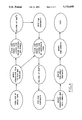
- Steps used in the construction of an exemplary backplate assembly 16, are illustrated in FIG. 4.
- the resulting structure of the backplate 16 is illustrated in more detail in FIGS. 5 and 6.
- the vias 92-102, in these figures are illustrated as positioned adjacent to each other in a straight line only for purposes of clarity. These vias may have a variety of configurations as disclosed above.
- a complete backplate structure requires RF signal feeds, logic control lines for phase shifters, and DC bias lines at a minimum.
- the backplate assembly 16 is shown having 7 layers of ceramic material 50-62 interposed between 8 metallic or conductive layers 70-84 to meet these requirements.
- layers may be employed within the teachings of the invention depending upon the specific application or circuit designs contemplated.
- the backplate 16 is constructed by preparing a series of individual ceramic layers using uncured, or green, ceramic material.
- the ceramic is chosen to have a thermal expansion roughly that of the MMIC wafer to minimize breaking and warping of MMIC sub-arrays.
- An exemplary material is an alumina compound in the form of uncured ceramic tape. While other ceramic materials can be employed, alumina compounds provide desirable Coefficients of Thermal Expansion (CTE) and structural properties. Alumina compounds can also be lapped or polished to achieve precision tolerances and are widely available at low cost. As an example, a 94% alumina compound has a CTE of about 6.0 (PPM/°C) and GaAs can be made with a CTE of about 5.8, which provides an excellent thermal match.
- CTE Coefficients of Thermal Expansion
- Each layer of ceramic 50-62 is generally provided in a thickness which is determined by particular signal isolation requirements of circuits positioned adjacent to that layer, such as voltage standoff, dielectric constant, and capacitance. Exemplary layer thicknesses for EHF applications are about 0.014-0.015 inches, although others may be used.
- the layers associated with the RF network are illustrated as being thicker than the remaining layers, to satisfy isolation and dielectric constant constraints. All layers typically have the same planar dimensions so that a uniform sized ceramic board is formed. However, the layers can be tailored for different shapes or specialized configurations.
- Each ceramic layer has one or more conduction via holes 92-102 stamped, drilled, or otherwise formed in it which are then filled with a conductive material 86 in liquid or fluid form.
- the vias are typically circular in cross-section but can have other geometric shapes where desired.
- the conductive material 86 forms interconnections between opposite sides of each layer and, therefore, between adjacent ceramic layers. These interconnections form hybrid conductive vias which are combined to provide a vast array of interconnections for the MMIC circuits 12 through which RF, DC bias, and control signals will be transferred.
- a preferred conductive material 86 is a conductive ink such as, but not limited, to a liquid gold or silver ink. The ink forms a solid at elevated temperatures when the ceramic material is heated or fired.
- the diameter or cross-sectional size of the vias 94-102 depends on the signal transfer requirements and include parameters such as resistance, current capacity, inductance, etc. For EHF applications, vias on the order of 0.013 inches are typical.
- Circuit patterns or interconnections for interfacing with or controlling a given set of MMIC elements or functions are formed on each interior ceramic layer. This is accomplished using known deposition, coating, or plating techniques to place metallic layers in the form of predetermined conductive patterns on the ceramic.
- An exemplary method uses conductive ink, which is deposited using known masking techniques. The ink is then dried during processing and forms a solid metal pattern. The metallic material can also be etched using known techniques. Each conductive ink, like any metal, has a different resistivity which determines its application. Inks found useful in realizing the invention are thick film silver, gold, or platinum/gold with resistivities on the order of 1.8, 12.7, and 85 milli-ohms per centimeter respectively.
- a small area of conductive material 90 is left adjacent to where the conductive vias 92-102 extend through the layers 50-60, respectively.
- This small, typically circular, conductive layer or button completes the connection between adjacent ceramic layers when the backplate 16 is assembled into a unitary structure.
- the contact area or button 90 is preferably wider than the cross-section of the vias to reduce alignment constraints and assure proper contact.
- An isolation gap 88 is provided around the via contacts 90 for adjacent surface contact isolation.
- an uppermost ceramic layer 50 closest to the MMIC, is used to support a RF ground plane or circuit 70 for a RF corporate stripline feed.
- a center conductor or interconnection circuit 72 for the RF feed is placed on the next ceramic material layer, 52.
- the pattern for the interconnection circuit can be adjusted to fit specific applications or requirements.
- One useful configuration is illustrated in general form in FIG. 7.
- a single RF input/output line is shown being power divided into a series of successively subdivided RF transfer lines in the case of a transmit array, and combined with preceding RF transfer lines in the case of a receive array.
- This structure allows the RF signal to be efficiently transferred between a single signal line and the thousands of elements found in a typical array.
- RF feed striplines are typically about 0.0005 inches thick and 0.016-0.030 inches wide to achieve a 40-50 ohms input/output line.
- junction structures can be employed for the power divider/combiner and for interfacing with the conductive vias, see below, as will be readily apparent to those skilled in the art. Junctions such as the Wilkinson Junction have been found useful to meet transfer needs or desired efficiencies at required bandwidth.
- the connections of the RF stripline conductors to the MMIC module 14 are provided by the conductive vias 92.
- the next adjacent ceramic layer 54 supports a second ground plane 74 to complete the overall RF stripline.
- the stripline is a low loss shielded structure in which susceptibility to external RF interference is minimized. RF coupling is typically less than -90 dB. This structure is also less susceptible to electromagnetic interference and electromagnetic coupling.
- the ceramic layers 56 and 58 support first and second amplifier bias connection layers or circuits 76 and 78, respectively, for amplifier drain and gate connections.
- the amplifier drain or ground bias is the same as one previously discussed RF ground which will reduce cross-talk among RF lines.
- each DC bias is connected by a via 96 or 98 which extends through the backplate 16, including the stripline RF feed 72. Once a given DC bias feedthrough reaches the MMIC module, it is connected to all amplifiers. This is illustrated using the vias 98a and 98b in FIG. 6. However, those skilled in the art will readily recognize that where a particular application desires separation of this connection, additional separately-connected conduction/ceramic layers can be provided.
- All of the ceramic layers separating the amplifier and phase control inputs are made thick enough to reduce phase control line capacitance and to increase the physical strength of the backplate 16 or arrays 10.
- Subsequent ceramic layers typically support control lines or conductive strips 80 and 82 for element phase control.
- the control lines 80 connect the phase control feedthrough vias 100 and 102 to the edge of the backplate 16 where they connect with phase control gate array integrated circuits 28.
- the integrated circuits 28 perform signal multiplexing or phase shifting, and are then connected to external circuitry through a unified connector.
- the last ceramic layer generally supports a metallic layer 84 which comprises an independent ground or shielding plane.
- phase control cabling is greatly reduced.
- every 4 MMIC elements 12 would require four cables and result in 4096 cables for an array of 4096 elements.
- 32 commercially available gate array logic integrated circuits are used on the array, typically eight on a side, only sixteen phase control cables or connections to external apparatus are needed.
- the use of backplate mounted and interconnected control logic by the present invention allows the number of cable wires to the backplate assembly to be reduced by a factor of about 100 or more.
- the phase control lines in the backplate 16 are surrounded by high thermal conductivity ceramic which allows for improved cooling. This is desirable because of the high data rates typically employed. For example, changing phase every 62.5 microseconds requires loading three to four bits per element at a 16 MHz rate.
- interconnection circuitry is deposited or formed on the separate layers, or as each is finished, they are aligned and stacked together into one form and "co-fired” at a high temperature to cure. This also causes the ceramic layers to fuse together to form a unitary multi-layer ceramic board with the RF, DC bias, and phase control networks embedded between layers. Alternatively, the individual layers can be "co-fired” as each additional layer is built or bonded using other known techniques once they are separately fired.
- the invention provides a greatly simplified electrical connection structure for an array apparatus because it can use one RF and one control and power connector.
- the off-array connections generally only require sixteen control, three power, and one ground connection each, respectively.
- the inventive method greatly reduces concerns over backplate handling since all critical RF and DC lines are buried within backplate layers.
- the ceramic backplate 16 is now joined to each MMIC module 14 by application of a thin layer of a solder compound 110 to the top of the RF ground layer 70. While the ceramic board is being heated to melt the solder 110, the MMIC module 14 is aligned and mounted on the backplate 16.
- An exemplary solder is indium solder which has a melting point of about 157° C.
- the alignment can be made optically through use of various edge alignment techniques, optical marks placed on the MMIC and ceramic during manufacture, or using notches or similar devices.
- each MMIC substrate 30 is also provided with the ground layer 42 which is firmly bonded to the GaAs material.
- the solder 110 acts to bond the two ground layers, 42 and 70, and, thus, the modules 14 and backplate 16 together. While less useful for thermodynamic reasons, other materials such as epoxy can be used to bond each MMIC module 14 to the backplate 16 for low thermal loading applications.
- FIG. 6 A composite view of an array structure is illustrated in FIG. 6.
- the backplate 16 and MMIC modules 14 are assembled together to form one phased array structure 10.
- a separate cold plate 112 is attached to the underside of the ceramic backplate 16.
- the cooling plate 112 is preferably an air-cooled heat sink with air channels 114.
- the cooling plate 112 provides both structural rigidity and heat dissipation for the array 10. By maintaining a low temperature, typically less than 100° C., the reliability of the MMIC elements 12 or modules 14 are greatly increased. Mechanical stress due to thermal build-up is also reduced.
- the plate 112 also offers a strong surface for mounting of electrical connectors for RF, DC bias, and any related control signals.
- the material used to manufacture the plate 112 needs to have a coefficient of expansion similar to that of the ceramic to prevent stress or warping.
- One method of addressing this problem is to use a metal laminate structure. This type of structure allows the composition of the heat sink to be adjusted to approximate or match the CTE of the ceramic. This leads to reduced stress from thermal loading and reduces backplate distortion of the heat sink to less than about 0.03 inches, or misalignment of the MMIC elements through substrate deflection to less than about 6 millionths of an inch. This in turn decreases array assembly 10 failure due to thermal or stress problems limiting reliability problems to the individual MMIC elements.
- An exemplary metal structure would be a copper-molybdinum-copper alloy with concentrations ranging between about 20/60/20 and 25/50/25 which provides CTE values of about 6.8 to 7.9 which compares well with the CTE values for the GaAs and ceramic materials discussed above.
- the overall thickness for the array 10 with the plate 112 added is typically on the order of 1.0 inch. This forms an array assembly thin enough to fit in confined or restricted spaces. At the same time, the array is light enough, between about 13 to 48 pounds for most applications, to meet most weight limitations and yet strong enough to handle most surface loads.
- the array 10 or sub-array 14 can also be curved or otherwise configured to various surface shapes by shaping the cooling plate 112 and the ceramic layers prior to curing. At the same time, the array 10 can obtain an extremely flat profile.
- the monolithic via hole technology on a ceramic substrate provides a low cost and reliable backplate.
- the construction method requires no wiring which simplifies fabrication, creates significant labor/cost savings and improves reliability.
- the invention uses standard commerically available batch processing approaches and will solve many of the problems associated with making a massive amount of electrical interconnections for a large array of MMIC elements. It will also help with the process of assembling a large array from many sub-arrays.
- the invention achieves array-to-array performance consistency.
- the inventive structure also allows the backplate to be tested independent of sensitive MMIC sub-arrays.
- the assembly is not only easier to test, but as previously discussed can be tested in stages to monitor manufacturing operations. This reduces loss of MMICs due to pre-existing backplate damage while increasing delivered product reliability.
- RF feed and bias network configurations have been illustrated, and other configurations are possible. Additional ceramic layers or circuit feeding networks may be used for other array applications. This general feeding approach can also be extended to other transmission line applications. For example, a microstrip line can be deposited on a single layer of ceramic for an RF and DC feed network. In this case, a thinner ceramic backplate is used dependent upon applicable structural support requirements.
Landscapes
- Variable-Direction Aerials And Aerial Arrays (AREA)
Abstract
Description
Claims (13)
Priority Applications (1)
| Application Number | Priority Date | Filing Date | Title |
|---|---|---|---|
| US07/540,964 US5132648A (en) | 1990-06-08 | 1990-06-08 | Large array MMIC feedthrough |
Applications Claiming Priority (1)
| Application Number | Priority Date | Filing Date | Title |
|---|---|---|---|
| US07/540,964 US5132648A (en) | 1990-06-08 | 1990-06-08 | Large array MMIC feedthrough |
Publications (1)
| Publication Number | Publication Date |
|---|---|
| US5132648A true US5132648A (en) | 1992-07-21 |
Family
ID=24157641
Family Applications (1)
| Application Number | Title | Priority Date | Filing Date |
|---|---|---|---|
| US07/540,964 Expired - Lifetime US5132648A (en) | 1990-06-08 | 1990-06-08 | Large array MMIC feedthrough |
Country Status (1)
| Country | Link |
|---|---|
| US (1) | US5132648A (en) |
Cited By (40)
| Publication number | Priority date | Publication date | Assignee | Title |
|---|---|---|---|---|
| US5327152A (en) * | 1991-10-25 | 1994-07-05 | Itt Corporation | Support apparatus for an active aperture radar antenna |
| US5359488A (en) * | 1993-06-21 | 1994-10-25 | Westinghouse Electric Corporation | Packaging system for a standard electronic module |
| US5373299A (en) * | 1993-05-21 | 1994-12-13 | Trw Inc. | Low-profile wideband mode forming network |
| US5672083A (en) * | 1993-06-22 | 1997-09-30 | Candescent Technologies Corporation | Fabrication of flat panel device having backplate that includes ceramic layer |
| US5774340A (en) * | 1996-08-28 | 1998-06-30 | International Business Machines Corporation | Planar redistribution structure and printed wiring device |
| US5898412A (en) * | 1996-08-02 | 1999-04-27 | Ericsson Inc. | Transmit/receive antenna mounting enclosure |
| US6324755B1 (en) * | 1999-06-17 | 2001-12-04 | Raytheon Company | Solid interface module |
| US6421253B1 (en) * | 2000-09-08 | 2002-07-16 | Powerwave Technologies, Inc. | Durable laminated electronics assembly using epoxy preform |
| US20020167070A1 (en) * | 2000-06-30 | 2002-11-14 | Motorola, Inc. | Hybrid semiconductor structure and device |
| US6512431B2 (en) | 2001-02-28 | 2003-01-28 | Lockheed Martin Corporation | Millimeterwave module compact interconnect |
| WO2003009421A1 (en) * | 2001-07-16 | 2003-01-30 | Motorola, Inc. | Apparatus for effecting transfer of electromagnetic energy |
| US6555946B1 (en) | 2000-07-24 | 2003-04-29 | Motorola, Inc. | Acoustic wave device and process for forming the same |
| US20030122638A1 (en) * | 2001-12-27 | 2003-07-03 | Yukinobu Tarui | Stacked radio-frequency module |
| US6590236B1 (en) | 2000-07-24 | 2003-07-08 | Motorola, Inc. | Semiconductor structure for use with high-frequency signals |
| US6589856B2 (en) | 2001-08-06 | 2003-07-08 | Motorola, Inc. | Method and apparatus for controlling anti-phase domains in semiconductor structures and devices |
| US20030169134A1 (en) * | 2002-03-05 | 2003-09-11 | Xytrans, Inc. | Millimeter wave (MMW) radio frequency transceiver module and method of forming same |
| US6639249B2 (en) | 2001-08-06 | 2003-10-28 | Motorola, Inc. | Structure and method for fabrication for a solid-state lighting device |
| US6638838B1 (en) | 2000-10-02 | 2003-10-28 | Motorola, Inc. | Semiconductor structure including a partially annealed layer and method of forming the same |
| US6646293B2 (en) | 2001-07-18 | 2003-11-11 | Motorola, Inc. | Structure for fabricating high electron mobility transistors utilizing the formation of complaint substrates |
| US6645790B2 (en) * | 2001-01-03 | 2003-11-11 | Anadigics, Inc. | System and method for prototyping and fabricating complex microwave circuits |
| US20030224559A1 (en) * | 2002-05-28 | 2003-12-04 | Applied Materials, Inc. | Micromachined structures including glass vias with internal conductive layers anodically bonded to silicon-containing substrates |
| US6667196B2 (en) | 2001-07-25 | 2003-12-23 | Motorola, Inc. | Method for real-time monitoring and controlling perovskite oxide film growth and semiconductor structure formed using the method |
| US6673667B2 (en) | 2001-08-15 | 2004-01-06 | Motorola, Inc. | Method for manufacturing a substantially integral monolithic apparatus including a plurality of semiconductor materials |
| US6673646B2 (en) | 2001-02-28 | 2004-01-06 | Motorola, Inc. | Growth of compound semiconductor structures on patterned oxide films and process for fabricating same |
| US6693298B2 (en) | 2001-07-20 | 2004-02-17 | Motorola, Inc. | Structure and method for fabricating epitaxial semiconductor on insulator (SOI) structures and devices utilizing the formation of a compliant substrate for materials used to form same |
| US6693033B2 (en) | 2000-02-10 | 2004-02-17 | Motorola, Inc. | Method of removing an amorphous oxide from a monocrystalline surface |
| US6709989B2 (en) | 2001-06-21 | 2004-03-23 | Motorola, Inc. | Method for fabricating a semiconductor structure including a metal oxide interface with silicon |
| US20040182513A1 (en) * | 2003-03-21 | 2004-09-23 | Barnes Ted W. | Measurement of etching |
| US6977950B1 (en) * | 1999-11-29 | 2005-12-20 | Lucent Technologies Inc. | Power distribution network for optoelectronic circuits |
| US20060182386A1 (en) * | 2005-02-15 | 2006-08-17 | Stenger Peter A | Transmission line to waveguide interconnect and method of forming same |
| US20090135085A1 (en) * | 2007-09-17 | 2009-05-28 | Raby Scott A | Rhombic shaped, modularly expandable phased array antenna and method therefor |
| US7696062B2 (en) | 2007-07-25 | 2010-04-13 | Northrop Grumman Systems Corporation | Method of batch integration of low dielectric substrates with MMICs |
| US20110102967A1 (en) * | 2009-10-29 | 2011-05-05 | Medtronic, Inc. | Implantable co-fired electrical feedthroughs |
| WO2013032813A1 (en) * | 2011-08-30 | 2013-03-07 | Harris Corporation | Phased array antenna module and method of making same |
| US20140198832A1 (en) * | 2010-07-12 | 2014-07-17 | Blackberry Limited | Multiple Input Multiple Output Antenna Module and Associated Method |
| US9136595B2 (en) | 2011-07-15 | 2015-09-15 | Blackberry Limited | Diversity antenna module and associated method for a user equipment (UE) device |
| US20150303586A1 (en) * | 2014-04-17 | 2015-10-22 | The Boeing Company | Modular antenna assembly |
| US9748668B2 (en) | 2011-07-15 | 2017-08-29 | Blackberry Limited | Diversity antenna module and associated method for a user equipment (UE) device |
| CN108462475A (en) * | 2017-02-21 | 2018-08-28 | 波音公司 | 3D small throughputs, high power mmic amplifier |
| US20180309210A1 (en) * | 2017-04-24 | 2018-10-25 | Murata Manufacturing Co., Ltd. | Array antenna |
Citations (12)
| Publication number | Priority date | Publication date | Assignee | Title |
|---|---|---|---|---|
| US3777220A (en) * | 1972-06-30 | 1973-12-04 | Ibm | Circuit panel and method of construction |
| US4371744A (en) * | 1977-10-03 | 1983-02-01 | Compagnie Internationale Pour L'informatique Cii-Honeywell Bull (Societe Anonyme) | Substrate for interconnecting electronic integrated circuit components having a repair arrangement enabling modification of connections to a mounted chip device |
| US4407007A (en) * | 1981-05-28 | 1983-09-27 | International Business Machines Corporation | Process and structure for minimizing delamination in the fabrication of multi-layer ceramic substrate |
| US4636755A (en) * | 1984-07-26 | 1987-01-13 | Motorola, Inc. | High-ratio, isolated microwave branch coupler with power divider, phase shifters, and quadrature hybrid |
| US4724283A (en) * | 1985-09-27 | 1988-02-09 | Nec Corporation | Multi-layer circuit board having a large heat dissipation |
| US4725925A (en) * | 1983-12-26 | 1988-02-16 | Hitachi, Ltd. | Circuit board |
| US4821142A (en) * | 1986-06-06 | 1989-04-11 | Hitachi, Ltd. | Ceramic multilayer circuit board and semiconductor module |
| US4837408A (en) * | 1987-05-21 | 1989-06-06 | Ngk Spark Plug Co., Ltd. | High density multilayer wiring board and the manufacturing thereof |
| US4899118A (en) * | 1988-12-27 | 1990-02-06 | Hughes Aircraft Company | Low temperature cofired ceramic packages for microwave and millimeter wave gallium arsenide integrated circuits |
| US4907128A (en) * | 1988-12-15 | 1990-03-06 | Grumman Aerospace Corporation | Chip to multilevel circuit board bonding |
| US4922377A (en) * | 1987-11-16 | 1990-05-01 | Hitachi, Ltd. | Module and a substrate for the module |
| US4929959A (en) * | 1988-03-08 | 1990-05-29 | Communications Satellite Corporation | Dual-polarized printed circuit antenna having its elements capacitively coupled to feedlines |
-
1990
- 1990-06-08 US US07/540,964 patent/US5132648A/en not_active Expired - Lifetime
Patent Citations (12)
| Publication number | Priority date | Publication date | Assignee | Title |
|---|---|---|---|---|
| US3777220A (en) * | 1972-06-30 | 1973-12-04 | Ibm | Circuit panel and method of construction |
| US4371744A (en) * | 1977-10-03 | 1983-02-01 | Compagnie Internationale Pour L'informatique Cii-Honeywell Bull (Societe Anonyme) | Substrate for interconnecting electronic integrated circuit components having a repair arrangement enabling modification of connections to a mounted chip device |
| US4407007A (en) * | 1981-05-28 | 1983-09-27 | International Business Machines Corporation | Process and structure for minimizing delamination in the fabrication of multi-layer ceramic substrate |
| US4725925A (en) * | 1983-12-26 | 1988-02-16 | Hitachi, Ltd. | Circuit board |
| US4636755A (en) * | 1984-07-26 | 1987-01-13 | Motorola, Inc. | High-ratio, isolated microwave branch coupler with power divider, phase shifters, and quadrature hybrid |
| US4724283A (en) * | 1985-09-27 | 1988-02-09 | Nec Corporation | Multi-layer circuit board having a large heat dissipation |
| US4821142A (en) * | 1986-06-06 | 1989-04-11 | Hitachi, Ltd. | Ceramic multilayer circuit board and semiconductor module |
| US4837408A (en) * | 1987-05-21 | 1989-06-06 | Ngk Spark Plug Co., Ltd. | High density multilayer wiring board and the manufacturing thereof |
| US4922377A (en) * | 1987-11-16 | 1990-05-01 | Hitachi, Ltd. | Module and a substrate for the module |
| US4929959A (en) * | 1988-03-08 | 1990-05-29 | Communications Satellite Corporation | Dual-polarized printed circuit antenna having its elements capacitively coupled to feedlines |
| US4907128A (en) * | 1988-12-15 | 1990-03-06 | Grumman Aerospace Corporation | Chip to multilevel circuit board bonding |
| US4899118A (en) * | 1988-12-27 | 1990-02-06 | Hughes Aircraft Company | Low temperature cofired ceramic packages for microwave and millimeter wave gallium arsenide integrated circuits |
Non-Patent Citations (2)
| Title |
|---|
| Mcllvenna, "Monolithic Phased Arrays for EHF Communications Terminals", Microwave Journal, Mar. 1988, pp. 113-117, 121-124. |
| Mcllvenna, Monolithic Phased Arrays for EHF Communications Terminals , Microwave Journal, Mar. 1988, pp. 113 117, 121 124. * |
Cited By (56)
| Publication number | Priority date | Publication date | Assignee | Title |
|---|---|---|---|---|
| US5327152A (en) * | 1991-10-25 | 1994-07-05 | Itt Corporation | Support apparatus for an active aperture radar antenna |
| US5373299A (en) * | 1993-05-21 | 1994-12-13 | Trw Inc. | Low-profile wideband mode forming network |
| US5359488A (en) * | 1993-06-21 | 1994-10-25 | Westinghouse Electric Corporation | Packaging system for a standard electronic module |
| US5672083A (en) * | 1993-06-22 | 1997-09-30 | Candescent Technologies Corporation | Fabrication of flat panel device having backplate that includes ceramic layer |
| US5686790A (en) * | 1993-06-22 | 1997-11-11 | Candescent Technologies Corporation | Flat panel device with ceramic backplate |
| US5898412A (en) * | 1996-08-02 | 1999-04-27 | Ericsson Inc. | Transmit/receive antenna mounting enclosure |
| US5774340A (en) * | 1996-08-28 | 1998-06-30 | International Business Machines Corporation | Planar redistribution structure and printed wiring device |
| US6324755B1 (en) * | 1999-06-17 | 2001-12-04 | Raytheon Company | Solid interface module |
| US6977950B1 (en) * | 1999-11-29 | 2005-12-20 | Lucent Technologies Inc. | Power distribution network for optoelectronic circuits |
| US6693033B2 (en) | 2000-02-10 | 2004-02-17 | Motorola, Inc. | Method of removing an amorphous oxide from a monocrystalline surface |
| US20020167070A1 (en) * | 2000-06-30 | 2002-11-14 | Motorola, Inc. | Hybrid semiconductor structure and device |
| US6555946B1 (en) | 2000-07-24 | 2003-04-29 | Motorola, Inc. | Acoustic wave device and process for forming the same |
| US6590236B1 (en) | 2000-07-24 | 2003-07-08 | Motorola, Inc. | Semiconductor structure for use with high-frequency signals |
| US6421253B1 (en) * | 2000-09-08 | 2002-07-16 | Powerwave Technologies, Inc. | Durable laminated electronics assembly using epoxy preform |
| US6638838B1 (en) | 2000-10-02 | 2003-10-28 | Motorola, Inc. | Semiconductor structure including a partially annealed layer and method of forming the same |
| US6645790B2 (en) * | 2001-01-03 | 2003-11-11 | Anadigics, Inc. | System and method for prototyping and fabricating complex microwave circuits |
| US6512431B2 (en) | 2001-02-28 | 2003-01-28 | Lockheed Martin Corporation | Millimeterwave module compact interconnect |
| US6673646B2 (en) | 2001-02-28 | 2004-01-06 | Motorola, Inc. | Growth of compound semiconductor structures on patterned oxide films and process for fabricating same |
| US6709989B2 (en) | 2001-06-21 | 2004-03-23 | Motorola, Inc. | Method for fabricating a semiconductor structure including a metal oxide interface with silicon |
| WO2003009421A1 (en) * | 2001-07-16 | 2003-01-30 | Motorola, Inc. | Apparatus for effecting transfer of electromagnetic energy |
| US6646293B2 (en) | 2001-07-18 | 2003-11-11 | Motorola, Inc. | Structure for fabricating high electron mobility transistors utilizing the formation of complaint substrates |
| US6693298B2 (en) | 2001-07-20 | 2004-02-17 | Motorola, Inc. | Structure and method for fabricating epitaxial semiconductor on insulator (SOI) structures and devices utilizing the formation of a compliant substrate for materials used to form same |
| US6667196B2 (en) | 2001-07-25 | 2003-12-23 | Motorola, Inc. | Method for real-time monitoring and controlling perovskite oxide film growth and semiconductor structure formed using the method |
| US6589856B2 (en) | 2001-08-06 | 2003-07-08 | Motorola, Inc. | Method and apparatus for controlling anti-phase domains in semiconductor structures and devices |
| US6639249B2 (en) | 2001-08-06 | 2003-10-28 | Motorola, Inc. | Structure and method for fabrication for a solid-state lighting device |
| US6673667B2 (en) | 2001-08-15 | 2004-01-06 | Motorola, Inc. | Method for manufacturing a substantially integral monolithic apparatus including a plurality of semiconductor materials |
| US20030122638A1 (en) * | 2001-12-27 | 2003-07-03 | Yukinobu Tarui | Stacked radio-frequency module |
| US6657523B2 (en) * | 2001-12-27 | 2003-12-02 | Mitsubishi Denki Kabushiki Kaisha | Stacked radio-frequency module |
| US20050024166A1 (en) * | 2002-03-05 | 2005-02-03 | Xytrans, Inc. | Millimeter wave (MMW) radio frequency transceiver module and method of forming same |
| US6788171B2 (en) | 2002-03-05 | 2004-09-07 | Xytrans, Inc. | Millimeter wave (MMW) radio frequency transceiver module and method of forming same |
| US20030169134A1 (en) * | 2002-03-05 | 2003-09-11 | Xytrans, Inc. | Millimeter wave (MMW) radio frequency transceiver module and method of forming same |
| US7180394B2 (en) | 2002-03-05 | 2007-02-20 | Xytrans, Inc. | Millimeter wave (MMW) radio frequency transceiver module and method of forming same |
| US6759309B2 (en) | 2002-05-28 | 2004-07-06 | Applied Materials, Inc. | Micromachined structures including glass vias with internal conductive layers anodically bonded to silicon-containing substrates |
| US20030224559A1 (en) * | 2002-05-28 | 2003-12-04 | Applied Materials, Inc. | Micromachined structures including glass vias with internal conductive layers anodically bonded to silicon-containing substrates |
| US20040182513A1 (en) * | 2003-03-21 | 2004-09-23 | Barnes Ted W. | Measurement of etching |
| US7494596B2 (en) * | 2003-03-21 | 2009-02-24 | Hewlett-Packard Development Company, L.P. | Measurement of etching |
| US20090127225A1 (en) * | 2003-03-21 | 2009-05-21 | Barnes Ted W | Measurement of etching |
| US8173032B2 (en) | 2003-03-21 | 2012-05-08 | Hewlett-Packard Development Company, L.P. | Measurement of etching |
| US20060182386A1 (en) * | 2005-02-15 | 2006-08-17 | Stenger Peter A | Transmission line to waveguide interconnect and method of forming same |
| US7479841B2 (en) | 2005-02-15 | 2009-01-20 | Northrop Grumman Corporation | Transmission line to waveguide interconnect and method of forming same including a heat spreader |
| US7696062B2 (en) | 2007-07-25 | 2010-04-13 | Northrop Grumman Systems Corporation | Method of batch integration of low dielectric substrates with MMICs |
| US8081134B2 (en) * | 2007-09-17 | 2011-12-20 | The Boeing Company | Rhomboidal shaped, modularly expandable phased array antenna and method therefor |
| US20090135085A1 (en) * | 2007-09-17 | 2009-05-28 | Raby Scott A | Rhombic shaped, modularly expandable phased array antenna and method therefor |
| US20110102967A1 (en) * | 2009-10-29 | 2011-05-05 | Medtronic, Inc. | Implantable co-fired electrical feedthroughs |
| US8373075B2 (en) | 2009-10-29 | 2013-02-12 | Medtronic, Inc. | Implantable co-fired electrical feedthroughs |
| US9319155B2 (en) * | 2010-07-12 | 2016-04-19 | Blackberry Limited | Multiple input multiple output antenna module and associated method |
| US20140198832A1 (en) * | 2010-07-12 | 2014-07-17 | Blackberry Limited | Multiple Input Multiple Output Antenna Module and Associated Method |
| US9136595B2 (en) | 2011-07-15 | 2015-09-15 | Blackberry Limited | Diversity antenna module and associated method for a user equipment (UE) device |
| US9748668B2 (en) | 2011-07-15 | 2017-08-29 | Blackberry Limited | Diversity antenna module and associated method for a user equipment (UE) device |
| US8786515B2 (en) | 2011-08-30 | 2014-07-22 | Harris Corporation | Phased array antenna module and method of making same |
| WO2013032813A1 (en) * | 2011-08-30 | 2013-03-07 | Harris Corporation | Phased array antenna module and method of making same |
| US20150303586A1 (en) * | 2014-04-17 | 2015-10-22 | The Boeing Company | Modular antenna assembly |
| US10658758B2 (en) * | 2014-04-17 | 2020-05-19 | The Boeing Company | Modular antenna assembly |
| CN108462475A (en) * | 2017-02-21 | 2018-08-28 | 波音公司 | 3D small throughputs, high power mmic amplifier |
| CN108462475B (en) * | 2017-02-21 | 2023-08-04 | 波音公司 | 3D Low-Throughput, High-Power MMIC Amplifier |
| US20180309210A1 (en) * | 2017-04-24 | 2018-10-25 | Murata Manufacturing Co., Ltd. | Array antenna |
Similar Documents
| Publication | Publication Date | Title |
|---|---|---|
| US5132648A (en) | Large array MMIC feedthrough | |
| US11757203B2 (en) | Low profile antenna apparatus | |
| US6175287B1 (en) | Direct backside interconnect for multiple chip assemblies | |
| KR100758554B1 (en) | 2-channel microwave transmit / receive module for active aperture in radar systems | |
| US12080661B2 (en) | Integrated structures with antenna elements and IC chips employing edge contact connections | |
| JP2018093491A (en) | Wireless communications package with integrated antenna array | |
| US20050219137A1 (en) | Antenna apparatus and method | |
| KR20220071979A (en) | Antenna device with integrated antenna array and low loss multilayer interposer | |
| JP7524478B2 (en) | Integrated antenna array with beamformer IC chip having multiple surface boundaries - Patents.com | |
| US20060270279A1 (en) | Electrical connector apparatus and method | |
| WO2000039893A1 (en) | Phased array antenna and its manufacturing method | |
| US5262794A (en) | Monolithic gallium arsenide phased array using integrated gold post interconnects | |
| US20240154320A1 (en) | Antenna apparatus employing coplanar waveguide interconnect between rf components | |
| WO2024054268A1 (en) | Method of creating embedded components on an antenna substrate and antenna apparatus formed with same |
Legal Events
| Date | Code | Title | Description |
|---|---|---|---|
| AS | Assignment |
Owner name: ROCKWELL INTERNATIONAL CORPORATION Free format text: ASSIGNMENT OF ASSIGNORS INTEREST.;ASSIGNORS:TRINH, TRANG N.;SMITH, ELROY C. JR.;REEL/FRAME:005379/0317 Effective date: 19900604 |
|
| STCF | Information on status: patent grant |
Free format text: PATENTED CASE |
|
| FPAY | Fee payment |
Year of fee payment: 4 |
|
| FEPP | Fee payment procedure |
Free format text: PAYOR NUMBER ASSIGNED (ORIGINAL EVENT CODE: ASPN); ENTITY STATUS OF PATENT OWNER: LARGE ENTITY |
|
| AS | Assignment |
Owner name: CREDIT SUISSE FIRST BOSTON, NEW YORK Free format text: SECURITY INTEREST;ASSIGNORS:CONEXANT SYSTEMS, INC.;BROOKTREE CORPORATION;BROOKTREE WORLDWIDE SALES CORPORATION;AND OTHERS;REEL/FRAME:009719/0537 Effective date: 19981221 |
|
| AS | Assignment |
Owner name: CONEXANT SYSTEMS, INC., CALIFORNIA Free format text: ASSIGNMENT OF ASSIGNORS INTEREST;ASSIGNOR:ROCKWELL SCIENCE CENTER, LLC;REEL/FRAME:010415/0761 Effective date: 19981210 |
|
| FPAY | Fee payment |
Year of fee payment: 8 |
|
| AS | Assignment |
Owner name: BOEING COMPANY, THE, CALIFORNIA Free format text: MERGER;ASSIGNORS:ROCKWELL INTERNATIONAL CORPORATION;BOEING NORTH AMERICAN, INC.;REEL/FRAME:011164/0426;SIGNING DATES FROM 19961206 TO 19991230 |
|
| AS | Assignment |
Owner name: CONEXANT SYSTEMS, INC., CALIFORNIA Free format text: RELEASE OF SECURITY INTEREST;ASSIGNOR:CREDIT SUISSE FIRST BOSTON;REEL/FRAME:012252/0413 Effective date: 20011018 Owner name: BROOKTREE CORPORATION, CALIFORNIA Free format text: RELEASE OF SECURITY INTEREST;ASSIGNOR:CREDIT SUISSE FIRST BOSTON;REEL/FRAME:012252/0413 Effective date: 20011018 Owner name: BROOKTREE WORLDWIDE SALES CORPORATION, CALIFORNIA Free format text: RELEASE OF SECURITY INTEREST;ASSIGNOR:CREDIT SUISSE FIRST BOSTON;REEL/FRAME:012252/0413 Effective date: 20011018 Owner name: CONEXANT SYSTEMS WORLDWIDE, INC., CALIFORNIA Free format text: RELEASE OF SECURITY INTEREST;ASSIGNOR:CREDIT SUISSE FIRST BOSTON;REEL/FRAME:012252/0413 Effective date: 20011018 |
|
| AS | Assignment |
Owner name: CONEXANT SYSTEMS, INC., CALIFORNIA Free format text: SECURITY INTEREST;ASSIGNOR:ALPHA INDUSTRIES, INC.;REEL/FRAME:013240/0860 Effective date: 20020625 |
|
| AS | Assignment |
Owner name: ALPHA INDUSTRIES, INC., MASSACHUSETTS Free format text: RELEASE AND RECONVEYANCE/SECURITY INTEREST;ASSIGNOR:CONEXANT SYSTEMS, INC.;REEL/FRAME:014580/0880 Effective date: 20030307 |
|
| FPAY | Fee payment |
Year of fee payment: 12 |