US4763018A - Transistor constant bias circuits - Google Patents
Transistor constant bias circuits Download PDFInfo
- Publication number
- US4763018A US4763018A US07/011,098 US1109887A US4763018A US 4763018 A US4763018 A US 4763018A US 1109887 A US1109887 A US 1109887A US 4763018 A US4763018 A US 4763018A
- Authority
- US
- United States
- Prior art keywords
- collector
- transistor
- bias
- circuit
- npn
- Prior art date
- Legal status (The legal status is an assumption and is not a legal conclusion. Google has not performed a legal analysis and makes no representation as to the accuracy of the status listed.)
- Expired - Lifetime
Links
Images

Classifications
-
- G—PHYSICS
- G05—CONTROLLING; REGULATING
- G05F—SYSTEMS FOR REGULATING ELECTRIC OR MAGNETIC VARIABLES
- G05F3/00—Non-retroactive systems for regulating electric variables by using an uncontrolled element, or an uncontrolled combination of elements, such element or such combination having self-regulating properties
- G05F3/02—Regulating voltage or current
- G05F3/08—Regulating voltage or current wherein the variable is DC
- G05F3/10—Regulating voltage or current wherein the variable is DC using uncontrolled devices with non-linear characteristics
- G05F3/16—Regulating voltage or current wherein the variable is DC using uncontrolled devices with non-linear characteristics being semiconductor devices
- G05F3/20—Regulating voltage or current wherein the variable is DC using uncontrolled devices with non-linear characteristics being semiconductor devices using diode- transistor combinations
- G05F3/30—Regulators using the difference between the base-emitter voltages of two bipolar transistors operating at different current densities
Definitions
- the present invention concerns improvements in or relating to bias circuits, notably circuits that will provide constant bias current and will operate from a low supply voltage--e.g. a supply voltage of the order 0.9 volts.
- bias circuit When designing circuits, the need often arises to generate a supply-independent current bias.
- FIG. 1 A known design of bias circuit is shown in FIG. 1. The arrangement is that described in United Kingdom Patent Application GB No. 2007055.
- the circuit shown comprises a bias transistor T1, the collector load of which includes a pair of resistors R1, R2, which latter serve as a voltage/current divider. Feedback voltage/current is taken from the junction of the pair of resistors R1, R2 and is applied to the base of the bias transistor T1.
- the voltage/current, at the collector output of the bias transistor T1 is referred to the base of a drive transistor T2.
- the first resistor R1 is connected to the supply voltage rail Vs, and the emitters of the two transistors T1, T2, both NPN type bipolar transistors, are connected to circuit earth.
- the drive transistor T2 serves thus as a current sink.
- This bias circuit has a peaked current versus supply voltage characteristic, the characteristic C1 shown in FIG. 3. For practical purposes this bias circuit thus provides current that is reasonably constant over a limited range of supply voltage in the region of the characteristic maximum.
- the resistor values are chosen so that the range of supply voltage matches the working range of the circuit application, but because of the peaked nature of the characteristic the working range is necessarily much restricted, and applications therefore severely limited.
- the current value may be scaled by appropriate choice of the ratio of transistor emitter areas.
- the PNP inverse of the above circuit is also known, and may be employed as a current source.
- the circuit of figure comprises a PNP bias circuit including a bias transistor T1', a pair of collector load and base feedback resistors R1', R2' and a drive transistor T2'.
- This circuit is cascaded to the NPN circuit of FIG. 1 just described, the drive transistor T2' replacing the first resistor R1.
- This circuit has a twin-peaked characteristic--characteristic C2 shown in FIG. 3. Although this has an improved response, the peaking can be most pronounced when the circuit is overcompensated, and great care therefore must be taken in selecting the circuit components.
- the present invention is intended to provide a bias circuit capable of operation at low supply voltage--e.g. a supply voltage of the order 0.9 volts--and of supplying bias current reasonably constant in value independent of supply voltage and transistor parameters.
- a bias circuit comprising:
- a resistor in the collector path of the bias transistor, connected to apply feedback to the base of the
- an NPN-type bipolar drive transistor the base of which is connected to the collector of the bias transistor;
- a start-up current bias circuit connected to a point in the ring configuration.
- start-up circuit a circuit comprising: a bias transistor; a pair of resistors, in the collector path of the bias transistor, and connected to apply feedback to the base of the bias transistor; and, a drive transistor, the base of which is connected to the collector of the start-up bias transistor, the collector of which is connected to the point in the ring configuration.
- the start-up transistors may be NPN-type, for example, and may be connected thus to the collector of the NPN drive transistor of the bias circuit.
- FIGS. 1 and 2 are circuit diagrams for two known types of bias circuit
- FIG. 3 is a graph showing the current-voltage characteristics of the two circuits shown in the preceding FIGS. 1 and 2;
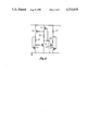
- FIG. 4 is a circuit diagram for a bias circuit modified in accord with this invention.
- a first bias transistor T1 has a feedback resistor R2 in its collector path, and the base of a first drive transistor T2 is connected to the collector output of the first bias transistor T1. Both these transistors are of NPN bipolar type and the end of the resistor R2 furthest from the collector is connected to the base of the first bias transistor to provide feedback. These components, which together form a first peaking current bias sub-circuit, are combined with a second peaking current bias sub-circuit, the PNP inverse of the first.
- This latter thus comprises a pair of PNP-type bipolar transistors, namely a second bias transistor T1' and a second drive transistor T2', the base of the latter T2' being connected to the collector output of the former T1' and a second resistor R2' being included in the collector path of the second bias transistor T1' and connected to the base of this transistor for feedback.
- the two peaking current bias sub-circuits are connected together in a ring configuration, the drive transistors T2, T2', in each case, being connected in the collector path of the bias transistors T1', T1, respectively, of the other sub-circuit.
- any suitable start-up circuit may be used for this purpose. It is convenient however to use a peaking current bias circuit of a somewhat similar construction to the first mentioned sub-circuit, this start-up circuit comprising a third bias transistor T1" and a third drive transistor T2" the base of which is connected to the collector of the third bias transistor T1" and the collector of which is connected to a point in the ring configuration--eg. to the collector of the first drive transistor T2, as shown.
- the collector path of the third transistor T1" includes a pair of third resistors R1", R2" which are connected in series between the collector and the supply rail Vs. Feedback is taken from the junction of these two resistors R1", R2" and applied to the base of the third bias transistor T1".
- a feature of the start-up circuit is that the value of the intermediate resistor R2" is inordinately high and such therefore that the characteristic of this start-up circuit peaks sharply and at very low supply voltage.
- This start-up circuit will thus provide a current peak as the supply voltage increases at start-up and no appreciable current loading thereafter as the supply voltage attains normal operating value.
- the intended application for the above described circuits is to integrated circuit design for Radio Paging Receivers.
- the circuit design for such devices is not straight forward due to low battery voltage requirements (end life 0.9 v) and low current consumption.
- the invention will find application to other low supply, low current circuits.
Landscapes
- Engineering & Computer Science (AREA)
- Microelectronics & Electronic Packaging (AREA)
- Physics & Mathematics (AREA)
- Power Engineering (AREA)
- Nonlinear Science (AREA)
- Electromagnetism (AREA)
- General Physics & Mathematics (AREA)
- Radar, Positioning & Navigation (AREA)
- Automation & Control Theory (AREA)
- Amplifiers (AREA)
Abstract
Description
______________________________________
R1" = 184 ohm;
              R2" = 89K ohm; T1" /T2" = 1:2
              R2' = 3K6 ohm; T1'/T2' = 1:4
              R2 = 1K8 ohm; T1/T2 = 1:1
______________________________________
Claims (3)
Applications Claiming Priority (2)
| Application Number | Priority Date | Filing Date | Title |
|---|---|---|---|
| GB8603112 | 1986-02-07 | ||
| GB8603112A GB2186756B (en) | 1986-02-07 | 1986-02-07 | Bias circuit |
Publications (1)
| Publication Number | Publication Date |
|---|---|
| US4763018A true US4763018A (en) | 1988-08-09 |
Family
ID=10592717
Family Applications (1)
| Application Number | Title | Priority Date | Filing Date |
|---|---|---|---|
| US07/011,098 Expired - Lifetime US4763018A (en) | 1986-02-07 | 1987-02-05 | Transistor constant bias circuits |
Country Status (2)
| Country | Link |
|---|---|
| US (1) | US4763018A (en) |
| GB (1) | GB2186756B (en) |
Cited By (9)
| Publication number | Priority date | Publication date | Assignee | Title |
|---|---|---|---|---|
| US4797577A (en) * | 1986-12-29 | 1989-01-10 | Motorola, Inc. | Bandgap reference circuit having higher-order temperature compensation |
| US5886570A (en) * | 1997-10-22 | 1999-03-23 | Analog Devices Inc | Inverter circuit biased to limit the maximum drive current to a following stage and method |
| US7026860B1 (en) * | 2003-05-08 | 2006-04-11 | O2Micro International Limited | Compensated self-biasing current generator |
| US20120047160A1 (en) * | 2010-08-17 | 2012-02-23 | Fujitsu Limited | Querying sensor data stored as binary decision diagrams |
| US20120046913A1 (en) * | 2010-08-17 | 2012-02-23 | Fujitsu Limited | Representing sensor data as binary decision diagrams |
| US9002781B2 (en) | 2010-08-17 | 2015-04-07 | Fujitsu Limited | Annotating environmental data represented by characteristic functions |
| US9075908B2 (en) | 2011-09-23 | 2015-07-07 | Fujitsu Limited | Partitioning medical binary decision diagrams for size optimization |
| US9138143B2 (en) | 2010-08-17 | 2015-09-22 | Fujitsu Limited | Annotating medical data represented by characteristic functions |
| US9176819B2 (en) | 2011-09-23 | 2015-11-03 | Fujitsu Limited | Detecting sensor malfunctions using compression analysis of binary decision diagrams |
Families Citing this family (2)
| Publication number | Priority date | Publication date | Assignee | Title |
|---|---|---|---|---|
| US5545978A (en) * | 1994-06-27 | 1996-08-13 | International Business Machines Corporation | Bandgap reference generator having regulation and kick-start circuits |
| US11867571B2 (en) * | 2021-10-01 | 2024-01-09 | Nxp B.V. | Self-turn-on temperature detector circuit |
Citations (4)
| Publication number | Priority date | Publication date | Assignee | Title |
|---|---|---|---|---|
| US3939434A (en) * | 1974-08-23 | 1976-02-17 | Tektronix, Inc. | Wideband DC current amplifier |
| US3955108A (en) * | 1972-09-15 | 1976-05-04 | Rca Corporation | Transistor amplifier stage with device in its temperature compensated bias network used as preliminary amplifier |
| US4016435A (en) * | 1974-03-11 | 1977-04-05 | U.S. Philips Corporation | Current stabilizing arrangement |
| US4029974A (en) * | 1975-03-21 | 1977-06-14 | Analog Devices, Inc. | Apparatus for generating a current varying with temperature |
-
1986
- 1986-02-07 GB GB8603112A patent/GB2186756B/en not_active Expired
-
1987
- 1987-02-05 US US07/011,098 patent/US4763018A/en not_active Expired - Lifetime
Patent Citations (4)
| Publication number | Priority date | Publication date | Assignee | Title |
|---|---|---|---|---|
| US3955108A (en) * | 1972-09-15 | 1976-05-04 | Rca Corporation | Transistor amplifier stage with device in its temperature compensated bias network used as preliminary amplifier |
| US4016435A (en) * | 1974-03-11 | 1977-04-05 | U.S. Philips Corporation | Current stabilizing arrangement |
| US3939434A (en) * | 1974-08-23 | 1976-02-17 | Tektronix, Inc. | Wideband DC current amplifier |
| US4029974A (en) * | 1975-03-21 | 1977-06-14 | Analog Devices, Inc. | Apparatus for generating a current varying with temperature |
Cited By (11)
| Publication number | Priority date | Publication date | Assignee | Title |
|---|---|---|---|---|
| US4797577A (en) * | 1986-12-29 | 1989-01-10 | Motorola, Inc. | Bandgap reference circuit having higher-order temperature compensation |
| US5886570A (en) * | 1997-10-22 | 1999-03-23 | Analog Devices Inc | Inverter circuit biased to limit the maximum drive current to a following stage and method |
| US7026860B1 (en) * | 2003-05-08 | 2006-04-11 | O2Micro International Limited | Compensated self-biasing current generator |
| US20120047160A1 (en) * | 2010-08-17 | 2012-02-23 | Fujitsu Limited | Querying sensor data stored as binary decision diagrams |
| US20120046913A1 (en) * | 2010-08-17 | 2012-02-23 | Fujitsu Limited | Representing sensor data as binary decision diagrams |
| US8874607B2 (en) * | 2010-08-17 | 2014-10-28 | Fujitsu Limited | Representing sensor data as binary decision diagrams |
| US8930394B2 (en) * | 2010-08-17 | 2015-01-06 | Fujitsu Limited | Querying sensor data stored as binary decision diagrams |
| US9002781B2 (en) | 2010-08-17 | 2015-04-07 | Fujitsu Limited | Annotating environmental data represented by characteristic functions |
| US9138143B2 (en) | 2010-08-17 | 2015-09-22 | Fujitsu Limited | Annotating medical data represented by characteristic functions |
| US9075908B2 (en) | 2011-09-23 | 2015-07-07 | Fujitsu Limited | Partitioning medical binary decision diagrams for size optimization |
| US9176819B2 (en) | 2011-09-23 | 2015-11-03 | Fujitsu Limited | Detecting sensor malfunctions using compression analysis of binary decision diagrams |
Also Published As
| Publication number | Publication date |
|---|---|
| GB2186756B (en) | 1989-11-01 |
| GB2186756A (en) | 1987-08-19 |
| GB8603112D0 (en) | 1986-03-12 |
Similar Documents
| Publication | Publication Date | Title |
|---|---|---|
| US6784743B2 (en) | High frequency amplifier and frequency mixer | |
| US3743850A (en) | Integrated current supply circuit | |
| US4763018A (en) | Transistor constant bias circuits | |
| US3090926A (en) | Transistor amplifier with tunnel diode in emitter circuit | |
| US3392342A (en) | Transistor amplifier with gain stability | |
| US4078199A (en) | Device for supplying a regulated current | |
| US4833344A (en) | Low voltage bias circuit | |
| US4063147A (en) | Stabilized power supply circuit | |
| US4688001A (en) | High Efficiency, low distortion amplifier | |
| US4870533A (en) | Transistor protection circuit | |
| US4429270A (en) | Switched current source for sourcing current to and sinking current from an output node | |
| US4786856A (en) | Temperature compensated current source | |
| US4977336A (en) | Schmitt-trigger circuit having no discrete resistor | |
| US4221979A (en) | Non-inverting buffer circuits | |
| US3778646A (en) | Semiconductor logic circuit | |
| GB1324837A (en) | Negative voltage regulator adapted to be constructed as an integrated circuit | |
| US3636381A (en) | Transistorized load control circuit comprising high- and low-parallel voltage sources | |
| US4369380A (en) | Circuit for controlling a transistor static switch for d.c. loads with high turn-on current | |
| US4213068A (en) | Transistor saturation control | |
| US4460864A (en) | Voltage reference circuit | |
| US3978350A (en) | Dual mode solid state power switch | |
| US7012469B2 (en) | Integrated circuit device having high efficiency at the time of low power output | |
| WO1983004351A1 (en) | Current limiter and method for limiting current | |
| US3739292A (en) | Amplifier circuit using complementary symmetry transistors | |
| EP1262852B1 (en) | Current source |
Legal Events
| Date | Code | Title | Description |
|---|---|---|---|
| AS | Assignment |
Owner name: PLESSEY OVERSEAS LIMITED, VICARAGE LANE, ILFORD, E Free format text: ASSIGNMENT OF ASSIGNORS INTEREST.;ASSIGNOR:MOON, PHILIP A. K.;REEL/FRAME:004709/0061 Effective date: 19870205 |
|
| STCF | Information on status: patent grant |
Free format text: PATENTED CASE |
|
| FPAY | Fee payment |
Year of fee payment: 4 |
|
| AS | Assignment |
Owner name: PLESSEY SEMICONDUCTORS LIMITED, ENGLAND Free format text: ASSIGNMENT OF ASSIGNORS INTEREST.;ASSIGNOR:PLESSEY OVERSEAS LIMITED;REEL/FRAME:006258/0010 Effective date: 19920629 |
|
| FPAY | Fee payment |
Year of fee payment: 8 |
|
| AS | Assignment |
Owner name: CANADIAN IMPERIAL BANK OF COMMERCE, AS SECURED PAR Free format text: SECURITY INTEREST;ASSIGNOR:MITEL CORPORATION, A CORPORATION UNDER THE LAWS OF CANADA;REEL/FRAME:009445/0299 Effective date: 19980212 |
|
| AS | Assignment |
Owner name: CANADIAN IMPERIAL BANK OF COMMERCE, AS SECURED PAR Free format text: RE-RECORD TO CORRECT THE ASSIGNOR PREVIOUSLY RECORDED ON REEL 9445 FRAME 0299.;ASSIGNOR:MITEL SEMICONDUCTOR LIMITED;REEL/FRAME:009798/0040 Effective date: 19980212 |
|
| FPAY | Fee payment |
Year of fee payment: 12 |
|
| AS | Assignment |
Owner name: MITEL CORPORATION, CANADA Free format text: RELEASE BY SECURED PARTY;ASSIGNOR:CANADIAN IMPERIAL BANK OF COMMERCE;REEL/FRAME:011590/0406 Effective date: 20010216 Owner name: MITEL, INC., A DELAWARE CORPORATION, CANADA Free format text: RELEASE BY SECURED PARTY;ASSIGNOR:CANADIAN IMPERIAL BANK OF COMMERCE;REEL/FRAME:011590/0406 Effective date: 20010216 Owner name: MITEL SEMICONDUCTOR, INC., A DELAWARE CORPORATION, Free format text: RELEASE BY SECURED PARTY;ASSIGNOR:CANADIAN IMPERIAL BANK OF COMMERCE;REEL/FRAME:011590/0406 Effective date: 20010216 Owner name: MITEL SEMICONDUCTOR, LIMITED, CANADA Free format text: RELEASE BY SECURED PARTY;ASSIGNOR:CANADIAN IMPERIAL BANK OF COMMERCE;REEL/FRAME:011590/0406 Effective date: 20010216 Owner name: MITEL TELCOM LIMITED CORPORATION, CANADA Free format text: RELEASE BY SECURED PARTY;ASSIGNOR:CANADIAN IMPERIAL BANK OF COMMERCE;REEL/FRAME:011590/0406 Effective date: 20010216 Owner name: MITEL SEMICONDUCTOR AMERICAS, INC., A DELAWARE COR Free format text: RELEASE BY SECURED PARTY;ASSIGNOR:CANADIAN IMPERIAL BANK OF COMMERCE;REEL/FRAME:011590/0406 Effective date: 20010216 |
|
| AS | Assignment |
Owner name: INTEL CORPORATION, CALIFORNIA Free format text: ASSIGNMENT OF ASSIGNORS INTEREST;ASSIGNOR:ZARLINK SEMICONDUCTOR LIMITED;REEL/FRAME:018087/0174 Effective date: 20060714 |
|
| FEPP | Fee payment procedure |
Free format text: PAYOR NUMBER ASSIGNED (ORIGINAL EVENT CODE: ASPN); ENTITY STATUS OF PATENT OWNER: LARGE ENTITY |