US4711701A - Self-aligned transistor method - Google Patents
Self-aligned transistor method Download PDFInfo
- Publication number
- US4711701A US4711701A US06/908,071 US90807186A US4711701A US 4711701 A US4711701 A US 4711701A US 90807186 A US90807186 A US 90807186A US 4711701 A US4711701 A US 4711701A
- Authority
- US
- United States
- Prior art keywords
- metal
- dielectric
- layer
- substrate
- regions
- Prior art date
- Legal status (The legal status is an assumption and is not a legal conclusion. Google has not performed a legal analysis and makes no representation as to the accuracy of the status listed.)
- Expired - Fee Related
Links
Images


Classifications
-
- H—ELECTRICITY
- H10—SEMICONDUCTOR DEVICES; ELECTRIC SOLID-STATE DEVICES NOT OTHERWISE PROVIDED FOR
- H10D—INORGANIC ELECTRIC SEMICONDUCTOR DEVICES
- H10D30/00—Field-effect transistors [FET]
- H10D30/01—Manufacture or treatment
- H10D30/061—Manufacture or treatment of FETs having Schottky gates
- H10D30/0612—Manufacture or treatment of FETs having Schottky gates of lateral single-gate Schottky FETs
- H10D30/0614—Manufacture or treatment of FETs having Schottky gates of lateral single-gate Schottky FETs using processes wherein the final gate is made after the completion of the source and drain regions, e.g. gate-last processes using dummy gates
-
- H10P50/667—
Definitions
- the present invention relates to electronic semiconductor devices, and, more particularly, to methods of fabrication of self-aligned MESFET and vertical bipolar transistors.
- Metal semiconductor field effect transistors are commonly used in gallium arsenide (GaAs) digital integrated circuits and one of the factors restricting switching speeds is the parasitic source and drain resistance.
- the parasitic resistances can be lessened by decreasing the gate-to-source and gate-to-drain distances to much less than 1 ⁇ m; and such small distances typically require some sort of self-alignment of the gate with respect to the source and drain.
- vertical bipolar transistors silicon and GaAs
- the base resistance limits high frequency response but it can be lessened by decreasing the distance between the emitter and the external base contact. Again, self-alignment of the emitter with respect to the base contact is required for distance much less than 1 ⁇ m.
- Digest 194 covers a dummy SiO 2 gate with 0.1 ⁇ m of PCVD Si 3 N 4 , implants through the nitride to form the source and drain with the dummy gate and the vertical sidewalls of nitride masking the implant; thus the thickness of the nitride determines the distance from the dummy gate to the source and drain; and lastly the dummy gate is replaced with a Ti/Al gate.
- K. Yamasaki et al Self-Align Implantation for n + -Layer Technology (SAINT) for High-Speed GaAs ICs, 18 Elec. Lett.
- the SAINT method has a resist structure that does not stand up well to temperature during the SiO 2 sputter deposition and requires a difficult sidewall removal of SiO 2 that must avoid undercutting the FPM and etching nitride underneath.
- One variation that avoids the difficult sidewall SiO 2 removal is the substitution of SiO 2 evaporation for the second SiO 2 sputter deposition; but SiO 2 evaporation is itself a difficult step.
- the present invention provides a method of fabrication of self-aligned MESFET and vertical bipolar transistors by use of a dummy gate or emitter made with aluminum overhanging on titanium:tungsten, the aluminum determines source/drain or base implants and the titanium:tungsten determines the gate or emitter.
- the use of a two-metal dummy structure solves the problems of a resist dummy structure sensitivity to processing temperatures and of sidewall SiO 2 removal leading to undercutting of a resist dummy structure.
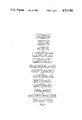
- FIG. 1 is a flow graph for a first preferred embodiment method of fabrication:
- FIGS. 2A-F illustrate the SAINT method in cross sectional elevation view
- FIGS. 3A-C illustrate the first preferred embodiment method in cross sectional elevation view
- FIGS. 4A-C illustrate the second preferred embodiment method in cross sectional elevation view.
- FIG. 1 is a flow graph for the steps of a first preferred embodiment method of fabrication for a GaAs MESFET. Details of the steps are described in connection with the discussion of FIGS. 3A-C, but first an explanation of the SAINT method is necessary.
- FIGS. 2A-F illustrate in schematic cross sectional elevation view the steps in the SAINT method:
- tri-level resist 40 consists of 0.8 ⁇ m thick layer 42 of spun-on FPM (or PMMA), 0.3 ⁇ m thick layer 44 of sputtered SiO 2 (or germanium), and a top layer 46 of spun-on photoresist. See FIG. 2B.
- Source 52 and drain 54 are now formed by implanting a dose of about 4 ⁇ 10 13 /cm 2 at 200 keV through silicon nitride layer 38 and using SiO 2 layer 44 as the implant mask; the overhang of layer 44 determines the distance between the foot of dummy gate 50 (FPM 42) and source 52 and drain 54. Then 0.3 ⁇ m thick layer 62 of SiO 2 is sputter deposited; this deposition also creates sidewall SiO 2 64 which is typically 100 ⁇ thick on FPM 42 and breadloaf-type SiO 2 deposits 66 on layer 44. See FIG. 2D. Note that dummy gate 50 may sag due to the temperatures of the SiO 2 sputter deposition. Deposition of SiO 2 62 under the overhang of layer 44 at the foot of dummy gate 50 is necessary to provide the eventual gate-to-source separation, so a perfectly vertical deposition is unworkable and sidewall SiO 2 64 is effectively unavoidable.
- Dummy gate 50 can be removed by dissolving FPM 42 to lift-off SiO 2 44 and 66, but first sidewall SiO 2 64 must be removed to expose FPM 42.
- a short etch with buffered HF Common Oxide Etch
- HF Common Oxide Etch
- the etch also undercuts the FPM base of dummy gate 50 (note that sidewall SiO 2 64 is thinner at the foot of dummy gate 50) and attacks silicon nitride 38.
- dummy gate 50 is removed by dissolution of FPM 42; see FIG. 2E.
- the implants are activated by an anneal at 800° C.; source and drain contact openings are cut in SiO 2 62/silicon nitride 38: ohmic metal 68 is deposited and lifted off; plasma etch the exposed portion of silicon nitride layer 38 down to GaAs 36 with SiO 2 62 providing the mask; and gate 70 is formed by titanium/platinum/gold deposition and lift-off. See FIG. 2F for completed MESFET 30.
- the first preferred embodiment method of fabrication is analogous to the SAINT method but uses a two-level metal resist instead of the tri-level resist 40 as follows:
- the active area 36 is formed (FIG. 2A) and silicon nitride layer 38 of thickness 0.05 ⁇ m is deposited as in SAINT.
- two-level resist 140 is formed by sputter deposition of alloy of 90% tungsten with 10% titanium (TiW) 142 to a thickness of 0.3 ⁇ m followed by spinning on and patterning photoresist for deposition and liftoff of 0.1 ⁇ m thick aluminum 144.
- the pattern of aluminum 144 regions defines the source and drain areas analogous to the patterning of photoresist 46 in SAINT step (c); see FIG. 3A in which the length (left to right) of aluminum 144 in the center of the figure is 1.5 ⁇ m.
- the aluminum 144 lift-off can be either silicon nitride assisted or with single or double level deep ultraviolet exposed resists; if nitride assisted lift-off is used, then the nitride is plasma etched off after the aluminum is lifted off.
- the titanium is alloyed with the tungsten to lessen the brittleness of the tungsten.
- TiW 142 is etched using a 30% solution of H 2 O 2 ; this undercuts aluminum 144 and is a very slow, highly controllable etch to form dummy gate 150.
- the 0.3 ⁇ m of TiW takes about twenty minutes to etch, and thus the amount of undercut can be easily adjusted. See FIG. 3B in which the foot of dummy gate 150 is 1.0 ⁇ m long.
- Source 52 and drain 54 are formed by implanting Si through silicon nitride layer 38; by adjusting the implant energy, the Si can also penetrate aluminum 144 to form a lighter doped extensions 53 and 55 of source 52 and drain 54, respectively, to improve the breakdown voltage of resulting MESFET 30. Note that for digital circuitry MESFETs do not have applied voltages greater than about 1 volt, so the depletion region in the GaAs about the Schottky gate effectively prevents lighter doped extensions 53 and 55 from forming short circuits to the gate.
- SiO 2 62 is sputter deposited to a thickness of 0.15 ⁇ m; as in SAINT, SiO 2 64 deposits on the sidewalls of TiW 142 and forms a breadloaf-type deposit 66 on aluminum 144. See FIG. 3C. Note that dummy gate 150 is all metal and is not affected by the sputtering temperatures. Alternatively, the SiO 2 could be deposited by plasma CVD or evaporation.
- step (d) Sidewall SiO 2 64 is removed by a short etch (about ten seconds) in dilute buffered HF. Note that TiW 142 is impervious to this etch and adheres very well to nitride layer 38, so no undercutting occurs. Once sidewall SiO 2 64 is removed, aluminum 144 is dissolved in an aqueous solution of NaOH, and TiW 142 is disolved in H 2 O 2 . This leaves the same structure as the completion of step (e) of SAINT; see FIG. 2E. The annealing, ohmic contacts, and Schottky gate formation are as in SAINT; see FIG. 2F. Note that silicon nitride 38 provides a cap on the GaAs during the annealing.
- the resulting MESFET 30 has a gate length of 1.0 ⁇ m with a gate-to-source and gate-to-drain separation of 0.25 ⁇ m.
- the Be implant must be of sufficient dose to convert the implanted portion of layer 135 to p + .
- the dimensions and shapes of the layers and the dummy structures could be varied widely, such as the 1.0 ⁇ m long foot of dummy gate 150 could be reduced to 0.2 ⁇ m by extending the undercut of the TiW. In this manner submicron features may be fabricated with optical lithography.
- Another example is the use of plasma etching in place of the wet etches of the preferred embodiments, such as CHCl 3 for plasma etching aluminum. The selectivity of the etches is probability better with wet etches, but selectivities do not have to be extraordinary because the dimensions of the structure can be designed to compensate for lower selectivity.
- the GaAs substrate could be Al xGa 1-x As, GaP, CdTe, Si or other semiconductors or more complex structures such as epitaxially GaAs grown on Si or GaAs on Si-on-sapphire; and the silicon dioxide and silicon nitride could be replaced by two other dielectrics provided that the appropriate selective etches are available.
- a third (or more) layer could be added to the dummy structure; and the silicon nitride layer could be omitted, except without the silicon nitride acting as a cap during the annealing of the implants some other provision such as an arsenic atmosphere would be needed.
- the silicon dioxide could be replaced by silicon nitride.
- MESFETs with offset gates can also be formed with the inventive method by using a angled deposition of aluminum after the dummy gate 150 has been removed; the shadow of the silicon dioxide 62 will leave an offset opening in the deposited aluminum which is then used to etch an opening in the silicon nitride 38 for the gate metal to contact the channel.
- the inventive methods have the advantages of metal dummy structures which are not affected like resists by high temperature processing and have good adherence to avoid undercutting during etching of the sidewall deposits.
Landscapes
- Junction Field-Effect Transistors (AREA)
Abstract
Description
Claims (10)
Priority Applications (1)
| Application Number | Priority Date | Filing Date | Title |
|---|---|---|---|
| US06/908,071 US4711701A (en) | 1986-09-16 | 1986-09-16 | Self-aligned transistor method |
Applications Claiming Priority (1)
| Application Number | Priority Date | Filing Date | Title |
|---|---|---|---|
| US06/908,071 US4711701A (en) | 1986-09-16 | 1986-09-16 | Self-aligned transistor method |
Publications (1)
| Publication Number | Publication Date |
|---|---|
| US4711701A true US4711701A (en) | 1987-12-08 |
Family
ID=25425119
Family Applications (1)
| Application Number | Title | Priority Date | Filing Date |
|---|---|---|---|
| US06/908,071 Expired - Fee Related US4711701A (en) | 1986-09-16 | 1986-09-16 | Self-aligned transistor method |
Country Status (1)
| Country | Link |
|---|---|
| US (1) | US4711701A (en) |
Cited By (43)
| Publication number | Priority date | Publication date | Assignee | Title |
|---|---|---|---|---|
| US4787958A (en) * | 1987-08-28 | 1988-11-29 | Motorola Inc. | Method of chemically etching TiW and/or TiWN |
| US4808545A (en) * | 1987-04-20 | 1989-02-28 | International Business Machines Corporation | High speed GaAs MESFET having refractory contacts and a self-aligned cold gate fabrication process |
| US4818712A (en) * | 1987-10-13 | 1989-04-04 | Northrop Corporation | Aluminum liftoff masking process and product |
| EP0220605A3 (en) * | 1985-10-21 | 1989-05-31 | Itt Industries Inc. | Method of making self-aligned gaas digital integrated circuits |
| US4874713A (en) * | 1989-05-01 | 1989-10-17 | Ncr Corporation | Method of making asymmetrically optimized CMOS field effect transistors |
| US5011785A (en) * | 1990-10-30 | 1991-04-30 | The United States Of America As Represented By The Secretary Of The Navy | Insulator assisted self-aligned gate junction |
| US5093272A (en) * | 1990-01-08 | 1992-03-03 | Siemens Aktiengesellschaft | Manufacturing method for a self-aligned emitter-base-complex for heterobipolar transistors |
| US5211807A (en) * | 1991-07-02 | 1993-05-18 | Microelectronics Computer & Technology | Titanium-tungsten etching solutions |
| US5278105A (en) * | 1992-08-19 | 1994-01-11 | Intel Corporation | Semiconductor device with dummy features in active layers |
| US5830797A (en) * | 1996-06-20 | 1998-11-03 | Cypress Semiconductor Corporation | Interconnect methods and apparatus |
| US5858843A (en) * | 1996-09-27 | 1999-01-12 | Intel Corporation | Low temperature method of forming gate electrode and gate dielectric |
| US5861676A (en) * | 1996-11-27 | 1999-01-19 | Cypress Semiconductor Corp. | Method of forming robust interconnect and contact structures in a semiconductor and/or integrated circuit |
| US5911887A (en) * | 1996-07-19 | 1999-06-15 | Cypress Semiconductor Corporation | Method of etching a bond pad |
| US6004874A (en) * | 1996-06-26 | 1999-12-21 | Cypress Semiconductor Corporation | Method for forming an interconnect |
| US6087208A (en) * | 1998-03-31 | 2000-07-11 | Advanced Micro Devices, Inc. | Method for increasing gate capacitance by using both high and low dielectric gate material |
| US6091129A (en) * | 1996-06-19 | 2000-07-18 | Cypress Semiconductor Corporation | Self-aligned trench isolated structure |
| DE19936005A1 (en) * | 1999-08-04 | 2001-02-08 | Daimler Chrysler Ag | FETs, especially for h.f. components, are produced by a low temperature self-aligned dummy gate sidewall-spaced process allowing various gate designs |
| US6187667B1 (en) | 1998-06-17 | 2001-02-13 | Cypress Semiconductor Corp. | Method of forming metal layer(s) and/or antireflective coating layer(s) on an integrated circuit |
| US6331495B1 (en) | 1998-01-22 | 2001-12-18 | Micron Technology, Inc. | Semiconductor structure useful in a self-aligned contact etch and method for making same |
| US6486066B2 (en) | 2001-02-02 | 2002-11-26 | Matrix Semiconductor, Inc. | Method of generating integrated circuit feature layout for improved chemical mechanical polishing |
| US6639257B2 (en) * | 1999-08-19 | 2003-10-28 | Hitachi, Ltd. | Hetero-junction bipolar transistor having a dummy electrode |
| US6673714B2 (en) * | 2002-04-25 | 2004-01-06 | Hewlett-Packard Development Company, L.P. | Method of fabricating a sub-lithographic sized via |
| US20040171244A1 (en) * | 1997-07-30 | 2004-09-02 | Micron Technology, Inc. | Selective spacer technology to prevent metal oxide formation during polycide reoxidation |
| US20050247976A1 (en) * | 2004-05-06 | 2005-11-10 | Ting Steve M | Notched spacer for CMOS transistors |
| US20080169512A1 (en) * | 2004-08-10 | 2008-07-17 | Doyle Brian S | Non-planar pMOS structure with a strained channel region and an integrated strained CMOS flow |
| US20080258176A1 (en) * | 2007-04-18 | 2008-10-23 | Yeong-Chang Chou | Antimonide-based compound semiconductor with titanium tungsten stack |
| US20090061572A1 (en) * | 2003-06-27 | 2009-03-05 | Intel Corporation | Nonplanar semiconductor device with partially or fully wrapped around gate electrode and methods of fabrication |
| US7736956B2 (en) | 2005-08-17 | 2010-06-15 | Intel Corporation | Lateral undercut of metal gate in SOI device |
| US7781771B2 (en) | 2004-03-31 | 2010-08-24 | Intel Corporation | Bulk non-planar transistor having strained enhanced mobility and methods of fabrication |
| US7858481B2 (en) * | 2005-06-15 | 2010-12-28 | Intel Corporation | Method for fabricating transistor with thinned channel |
| US7879675B2 (en) | 2005-03-14 | 2011-02-01 | Intel Corporation | Field effect transistor with metal source/drain regions |
| US7898041B2 (en) | 2005-06-30 | 2011-03-01 | Intel Corporation | Block contact architectures for nanoscale channel transistors |
| US7902014B2 (en) | 2005-09-28 | 2011-03-08 | Intel Corporation | CMOS devices with a single work function gate electrode and method of fabrication |
| US7989280B2 (en) | 2005-11-30 | 2011-08-02 | Intel Corporation | Dielectric interface for group III-V semiconductor device |
| US8067818B2 (en) | 2004-10-25 | 2011-11-29 | Intel Corporation | Nonplanar device with thinned lower body portion and method of fabrication |
| US8071983B2 (en) | 2005-06-21 | 2011-12-06 | Intel Corporation | Semiconductor device structures and methods of forming semiconductor structures |
| US8084818B2 (en) | 2004-06-30 | 2011-12-27 | Intel Corporation | High mobility tri-gate devices and methods of fabrication |
| US8183646B2 (en) | 2005-02-23 | 2012-05-22 | Intel Corporation | Field effect transistor with narrow bandgap source and drain regions and method of fabrication |
| US8268709B2 (en) | 2004-09-29 | 2012-09-18 | Intel Corporation | Independently accessed double-gate and tri-gate transistors in same process flow |
| US8362566B2 (en) | 2008-06-23 | 2013-01-29 | Intel Corporation | Stress in trigate devices using complimentary gate fill materials |
| US8405164B2 (en) | 2003-06-27 | 2013-03-26 | Intel Corporation | Tri-gate transistor device with stress incorporation layer and method of fabrication |
| US8617945B2 (en) | 2006-08-02 | 2013-12-31 | Intel Corporation | Stacking fault and twin blocking barrier for integrating III-V on Si |
| US20140011349A1 (en) * | 2012-07-05 | 2014-01-09 | Mitsubishi Electric Corporation | Method for manufacturing semiconductor device |
Citations (6)
| Publication number | Priority date | Publication date | Assignee | Title |
|---|---|---|---|---|
| US4387145A (en) * | 1981-09-28 | 1983-06-07 | Fairchild Camera & Instrument Corp. | Lift-off shadow mask |
| US4503599A (en) * | 1982-01-29 | 1985-03-12 | Hitachi, Ltd. | Method of fabricating field effect transistors |
| US4532004A (en) * | 1983-08-01 | 1985-07-30 | Kabushiki Kaisha Toshiba | Method of manufacturing a semiconductor device |
| US4561169A (en) * | 1982-07-30 | 1985-12-31 | Hitachi, Ltd. | Method of manufacturing semiconductor device utilizing multilayer mask |
| US4569124A (en) * | 1984-05-22 | 1986-02-11 | Hughes Aircraft Company | Method for forming thin conducting lines by ion implantation and preferential etching |
| US4597827A (en) * | 1984-02-29 | 1986-07-01 | Oki Electric Industry Co., Ltd. | Method of making MIS field effect transistor having a lightly-doped region |
-
1986
- 1986-09-16 US US06/908,071 patent/US4711701A/en not_active Expired - Fee Related
Patent Citations (6)
| Publication number | Priority date | Publication date | Assignee | Title |
|---|---|---|---|---|
| US4387145A (en) * | 1981-09-28 | 1983-06-07 | Fairchild Camera & Instrument Corp. | Lift-off shadow mask |
| US4503599A (en) * | 1982-01-29 | 1985-03-12 | Hitachi, Ltd. | Method of fabricating field effect transistors |
| US4561169A (en) * | 1982-07-30 | 1985-12-31 | Hitachi, Ltd. | Method of manufacturing semiconductor device utilizing multilayer mask |
| US4532004A (en) * | 1983-08-01 | 1985-07-30 | Kabushiki Kaisha Toshiba | Method of manufacturing a semiconductor device |
| US4597827A (en) * | 1984-02-29 | 1986-07-01 | Oki Electric Industry Co., Ltd. | Method of making MIS field effect transistor having a lightly-doped region |
| US4569124A (en) * | 1984-05-22 | 1986-02-11 | Hughes Aircraft Company | Method for forming thin conducting lines by ion implantation and preferential etching |
Cited By (81)
| Publication number | Priority date | Publication date | Assignee | Title |
|---|---|---|---|---|
| EP0220605A3 (en) * | 1985-10-21 | 1989-05-31 | Itt Industries Inc. | Method of making self-aligned gaas digital integrated circuits |
| US4808545A (en) * | 1987-04-20 | 1989-02-28 | International Business Machines Corporation | High speed GaAs MESFET having refractory contacts and a self-aligned cold gate fabrication process |
| US4787958A (en) * | 1987-08-28 | 1988-11-29 | Motorola Inc. | Method of chemically etching TiW and/or TiWN |
| US4818712A (en) * | 1987-10-13 | 1989-04-04 | Northrop Corporation | Aluminum liftoff masking process and product |
| US4874713A (en) * | 1989-05-01 | 1989-10-17 | Ncr Corporation | Method of making asymmetrically optimized CMOS field effect transistors |
| US5093272A (en) * | 1990-01-08 | 1992-03-03 | Siemens Aktiengesellschaft | Manufacturing method for a self-aligned emitter-base-complex for heterobipolar transistors |
| US5011785A (en) * | 1990-10-30 | 1991-04-30 | The United States Of America As Represented By The Secretary Of The Navy | Insulator assisted self-aligned gate junction |
| US5211807A (en) * | 1991-07-02 | 1993-05-18 | Microelectronics Computer & Technology | Titanium-tungsten etching solutions |
| US5278105A (en) * | 1992-08-19 | 1994-01-11 | Intel Corporation | Semiconductor device with dummy features in active layers |
| US6091129A (en) * | 1996-06-19 | 2000-07-18 | Cypress Semiconductor Corporation | Self-aligned trench isolated structure |
| US5830797A (en) * | 1996-06-20 | 1998-11-03 | Cypress Semiconductor Corporation | Interconnect methods and apparatus |
| US6004874A (en) * | 1996-06-26 | 1999-12-21 | Cypress Semiconductor Corporation | Method for forming an interconnect |
| US5911887A (en) * | 1996-07-19 | 1999-06-15 | Cypress Semiconductor Corporation | Method of etching a bond pad |
| US5858843A (en) * | 1996-09-27 | 1999-01-12 | Intel Corporation | Low temperature method of forming gate electrode and gate dielectric |
| US5861676A (en) * | 1996-11-27 | 1999-01-19 | Cypress Semiconductor Corp. | Method of forming robust interconnect and contact structures in a semiconductor and/or integrated circuit |
| US7009264B1 (en) * | 1997-07-30 | 2006-03-07 | Micron Technology, Inc. | Selective spacer to prevent metal oxide formation during polycide reoxidation |
| US7067411B2 (en) | 1997-07-30 | 2006-06-27 | Micron Technology, Inc. | Method to prevent metal oxide formation during polycide reoxidation |
| US20040171244A1 (en) * | 1997-07-30 | 2004-09-02 | Micron Technology, Inc. | Selective spacer technology to prevent metal oxide formation during polycide reoxidation |
| US6331495B1 (en) | 1998-01-22 | 2001-12-18 | Micron Technology, Inc. | Semiconductor structure useful in a self-aligned contact etch and method for making same |
| US6087208A (en) * | 1998-03-31 | 2000-07-11 | Advanced Micro Devices, Inc. | Method for increasing gate capacitance by using both high and low dielectric gate material |
| US6187667B1 (en) | 1998-06-17 | 2001-02-13 | Cypress Semiconductor Corp. | Method of forming metal layer(s) and/or antireflective coating layer(s) on an integrated circuit |
| DE19936005A1 (en) * | 1999-08-04 | 2001-02-08 | Daimler Chrysler Ag | FETs, especially for h.f. components, are produced by a low temperature self-aligned dummy gate sidewall-spaced process allowing various gate designs |
| US6639257B2 (en) * | 1999-08-19 | 2003-10-28 | Hitachi, Ltd. | Hetero-junction bipolar transistor having a dummy electrode |
| US6486066B2 (en) | 2001-02-02 | 2002-11-26 | Matrix Semiconductor, Inc. | Method of generating integrated circuit feature layout for improved chemical mechanical polishing |
| US6730931B2 (en) | 2001-02-02 | 2004-05-04 | Matix Semiconductor | Integrated circuit feature layout for improved chemical mechanical polishing |
| US20040173904A1 (en) * | 2001-02-02 | 2004-09-09 | Cleeves James M. | Integrated circuit feature layout for improved chemical mechanical polishing |
| US6982476B2 (en) | 2001-02-02 | 2006-01-03 | Matrix Semiconductor | Integrated circuit feature layout for improved chemical mechanical polishing |
| US6673714B2 (en) * | 2002-04-25 | 2004-01-06 | Hewlett-Packard Development Company, L.P. | Method of fabricating a sub-lithographic sized via |
| US8405164B2 (en) | 2003-06-27 | 2013-03-26 | Intel Corporation | Tri-gate transistor device with stress incorporation layer and method of fabrication |
| US20090061572A1 (en) * | 2003-06-27 | 2009-03-05 | Intel Corporation | Nonplanar semiconductor device with partially or fully wrapped around gate electrode and methods of fabrication |
| US7820513B2 (en) | 2003-06-27 | 2010-10-26 | Intel Corporation | Nonplanar semiconductor device with partially or fully wrapped around gate electrode and methods of fabrication |
| US8273626B2 (en) | 2003-06-27 | 2012-09-25 | Intel Corporationn | Nonplanar semiconductor device with partially or fully wrapped around gate electrode and methods of fabrication |
| US7781771B2 (en) | 2004-03-31 | 2010-08-24 | Intel Corporation | Bulk non-planar transistor having strained enhanced mobility and methods of fabrication |
| US20050247976A1 (en) * | 2004-05-06 | 2005-11-10 | Ting Steve M | Notched spacer for CMOS transistors |
| US8084818B2 (en) | 2004-06-30 | 2011-12-27 | Intel Corporation | High mobility tri-gate devices and methods of fabrication |
| US7960794B2 (en) | 2004-08-10 | 2011-06-14 | Intel Corporation | Non-planar pMOS structure with a strained channel region and an integrated strained CMOS flow |
| US20080169512A1 (en) * | 2004-08-10 | 2008-07-17 | Doyle Brian S | Non-planar pMOS structure with a strained channel region and an integrated strained CMOS flow |
| US8399922B2 (en) | 2004-09-29 | 2013-03-19 | Intel Corporation | Independently accessed double-gate and tri-gate transistors |
| US8268709B2 (en) | 2004-09-29 | 2012-09-18 | Intel Corporation | Independently accessed double-gate and tri-gate transistors in same process flow |
| US8067818B2 (en) | 2004-10-25 | 2011-11-29 | Intel Corporation | Nonplanar device with thinned lower body portion and method of fabrication |
| US8502351B2 (en) | 2004-10-25 | 2013-08-06 | Intel Corporation | Nonplanar device with thinned lower body portion and method of fabrication |
| US10236356B2 (en) | 2004-10-25 | 2019-03-19 | Intel Corporation | Nonplanar device with thinned lower body portion and method of fabrication |
| US9741809B2 (en) | 2004-10-25 | 2017-08-22 | Intel Corporation | Nonplanar device with thinned lower body portion and method of fabrication |
| US9190518B2 (en) | 2004-10-25 | 2015-11-17 | Intel Corporation | Nonplanar device with thinned lower body portion and method of fabrication |
| US8749026B2 (en) | 2004-10-25 | 2014-06-10 | Intel Corporation | Nonplanar device with thinned lower body portion and method of fabrication |
| US9614083B2 (en) | 2005-02-23 | 2017-04-04 | Intel Corporation | Field effect transistor with narrow bandgap source and drain regions and method of fabrication |
| US10121897B2 (en) | 2005-02-23 | 2018-11-06 | Intel Corporation | Field effect transistor with narrow bandgap source and drain regions and method of fabrication |
| US9368583B2 (en) | 2005-02-23 | 2016-06-14 | Intel Corporation | Field effect transistor with narrow bandgap source and drain regions and method of fabrication |
| US9748391B2 (en) | 2005-02-23 | 2017-08-29 | Intel Corporation | Field effect transistor with narrow bandgap source and drain regions and method of fabrication |
| US8368135B2 (en) | 2005-02-23 | 2013-02-05 | Intel Corporation | Field effect transistor with narrow bandgap source and drain regions and method of fabrication |
| US9048314B2 (en) | 2005-02-23 | 2015-06-02 | Intel Corporation | Field effect transistor with narrow bandgap source and drain regions and method of fabrication |
| US8816394B2 (en) | 2005-02-23 | 2014-08-26 | Intel Corporation | Field effect transistor with narrow bandgap source and drain regions and method of fabrication |
| US8183646B2 (en) | 2005-02-23 | 2012-05-22 | Intel Corporation | Field effect transistor with narrow bandgap source and drain regions and method of fabrication |
| US8664694B2 (en) | 2005-02-23 | 2014-03-04 | Intel Corporation | Field effect transistor with narrow bandgap source and drain regions and method of fabrication |
| US7879675B2 (en) | 2005-03-14 | 2011-02-01 | Intel Corporation | Field effect transistor with metal source/drain regions |
| US9806195B2 (en) | 2005-06-15 | 2017-10-31 | Intel Corporation | Method for fabricating transistor with thinned channel |
| US11978799B2 (en) | 2005-06-15 | 2024-05-07 | Tahoe Research, Ltd. | Method for fabricating transistor with thinned channel |
| US9337307B2 (en) | 2005-06-15 | 2016-05-10 | Intel Corporation | Method for fabricating transistor with thinned channel |
| US7858481B2 (en) * | 2005-06-15 | 2010-12-28 | Intel Corporation | Method for fabricating transistor with thinned channel |
| US10367093B2 (en) | 2005-06-15 | 2019-07-30 | Intel Corporation | Method for fabricating transistor with thinned channel |
| US10937907B2 (en) | 2005-06-15 | 2021-03-02 | Intel Corporation | Method for fabricating transistor with thinned channel |
| US8933458B2 (en) | 2005-06-21 | 2015-01-13 | Intel Corporation | Semiconductor device structures and methods of forming semiconductor structures |
| US9761724B2 (en) | 2005-06-21 | 2017-09-12 | Intel Corporation | Semiconductor device structures and methods of forming semiconductor structures |
| US8581258B2 (en) | 2005-06-21 | 2013-11-12 | Intel Corporation | Semiconductor device structures and methods of forming semiconductor structures |
| US9385180B2 (en) | 2005-06-21 | 2016-07-05 | Intel Corporation | Semiconductor device structures and methods of forming semiconductor structures |
| US8071983B2 (en) | 2005-06-21 | 2011-12-06 | Intel Corporation | Semiconductor device structures and methods of forming semiconductor structures |
| US7898041B2 (en) | 2005-06-30 | 2011-03-01 | Intel Corporation | Block contact architectures for nanoscale channel transistors |
| US7736956B2 (en) | 2005-08-17 | 2010-06-15 | Intel Corporation | Lateral undercut of metal gate in SOI device |
| US7902014B2 (en) | 2005-09-28 | 2011-03-08 | Intel Corporation | CMOS devices with a single work function gate electrode and method of fabrication |
| US8294180B2 (en) | 2005-09-28 | 2012-10-23 | Intel Corporation | CMOS devices with a single work function gate electrode and method of fabrication |
| US7989280B2 (en) | 2005-11-30 | 2011-08-02 | Intel Corporation | Dielectric interface for group III-V semiconductor device |
| US8617945B2 (en) | 2006-08-02 | 2013-12-31 | Intel Corporation | Stacking fault and twin blocking barrier for integrating III-V on Si |
| US8421121B2 (en) * | 2007-04-18 | 2013-04-16 | Northrop Grumman Systems Corporation | Antimonide-based compound semiconductor with titanium tungsten stack |
| US20080258176A1 (en) * | 2007-04-18 | 2008-10-23 | Yeong-Chang Chou | Antimonide-based compound semiconductor with titanium tungsten stack |
| US9450092B2 (en) | 2008-06-23 | 2016-09-20 | Intel Corporation | Stress in trigate devices using complimentary gate fill materials |
| US9224754B2 (en) | 2008-06-23 | 2015-12-29 | Intel Corporation | Stress in trigate devices using complimentary gate fill materials |
| US8741733B2 (en) | 2008-06-23 | 2014-06-03 | Intel Corporation | Stress in trigate devices using complimentary gate fill materials |
| US9806193B2 (en) | 2008-06-23 | 2017-10-31 | Intel Corporation | Stress in trigate devices using complimentary gate fill materials |
| US8362566B2 (en) | 2008-06-23 | 2013-01-29 | Intel Corporation | Stress in trigate devices using complimentary gate fill materials |
| US8987125B2 (en) * | 2012-07-05 | 2015-03-24 | Mitsubishi Electric Corporation | Method for manufacturing semiconductor device |
| US20140011349A1 (en) * | 2012-07-05 | 2014-01-09 | Mitsubishi Electric Corporation | Method for manufacturing semiconductor device |
Similar Documents
| Publication | Publication Date | Title |
|---|---|---|
| US4711701A (en) | Self-aligned transistor method | |
| US4711858A (en) | Method of fabricating a self-aligned metal-semiconductor FET having an insulator spacer | |
| US4656076A (en) | Self-aligned recessed gate process | |
| US4745082A (en) | Method of making a self-aligned MESFET using a substitutional gate with side walls | |
| JP2778600B2 (en) | Method for manufacturing semiconductor device | |
| US4997778A (en) | Process for forming a self-aligned FET having a T-shaped gate structure | |
| US4908325A (en) | Method of making heterojunction transistors with wide band-gap stop etch layer | |
| US4679311A (en) | Method of fabricating self-aligned field-effect transistor having t-shaped gate electrode, sub-micron gate length and variable drain to gate spacing | |
| JPH02148740A (en) | Semiconductor device and manufacture thereof | |
| JP2609267B2 (en) | Method of manufacturing self-aligned gallium arsenide device | |
| EP0338251A1 (en) | Method of manufacturing metal-semiconductor field effect transistors | |
| JP2677401B2 (en) | Method of manufacturing self-aligned gate FET | |
| US4616400A (en) | Process for fabricating a double recess channel field effect transistor | |
| US5550065A (en) | Method of fabricating self-aligned FET structure having a high temperature stable T-shaped Schottky gate contact | |
| JPH022142A (en) | Field effect transistor and its manufacturing method | |
| US5362658A (en) | Method for producing semiconductor device | |
| US5192701A (en) | Method of manufacturing field effect transistors having different threshold voltages | |
| US4642259A (en) | Source-side self-aligned gate process | |
| US4936781A (en) | Method of fabrication of a P+nn+ diode and of a bipolar transistor incorporating this diode utilizing the effect of neutralization of donor atoms by atomic hydrogen | |
| US5837570A (en) | Heterostructure semiconductor device and method of fabricating same | |
| US5640029A (en) | Field-effect transistor and method of producing same | |
| JPS58123779A (en) | Schottky gate field-effect transistor and its manufacture | |
| KR950000157B1 (en) | Manufacturing Method of Field Effect Transistor | |
| KR950005490B1 (en) | Enhancement/deplection type fet and its making method | |
| JPS62115782A (en) | Manufacture of semiconductor device |
Legal Events
| Date | Code | Title | Description |
|---|---|---|---|
| AS | Assignment |
Owner name: TEXAS INSTRUMENTS INCORPORATED, 13500 NORTH CENTRA Free format text: ASSIGNMENT OF ASSIGNORS INTEREST.;ASSIGNOR:MC LEVIGE, WILLIAM V.;REEL/FRAME:004604/0157 Effective date: 19860915 |
|
| FEPP | Fee payment procedure |
Free format text: PAYOR NUMBER ASSIGNED (ORIGINAL EVENT CODE: ASPN); ENTITY STATUS OF PATENT OWNER: LARGE ENTITY |
|
| FPAY | Fee payment |
Year of fee payment: 4 |
|
| FPAY | Fee payment |
Year of fee payment: 8 |
|
| REMI | Maintenance fee reminder mailed | ||
| LAPS | Lapse for failure to pay maintenance fees | ||
| FP | Lapsed due to failure to pay maintenance fee |
Effective date: 19991208 |
|
| STCH | Information on status: patent discontinuation |
Free format text: PATENT EXPIRED DUE TO NONPAYMENT OF MAINTENANCE FEES UNDER 37 CFR 1.362 |