US4497106A - Semiconductor device and a method of manufacturing the same - Google Patents
Semiconductor device and a method of manufacturing the same Download PDFInfo
- Publication number
- US4497106A US4497106A US06/315,903 US31590381A US4497106A US 4497106 A US4497106 A US 4497106A US 31590381 A US31590381 A US 31590381A US 4497106 A US4497106 A US 4497106A
- Authority
- US
- United States
- Prior art keywords
- forming
- bipolar transistor
- semiconductor device
- layer
- region
- Prior art date
- Legal status (The legal status is an assumption and is not a legal conclusion. Google has not performed a legal analysis and makes no representation as to the accuracy of the status listed.)
- Expired - Lifetime
Links
- 239000004065 semiconductor Substances 0.000 title claims abstract description 51
- 238000004519 manufacturing process Methods 0.000 title claims description 15
- 239000000758 substrate Substances 0.000 claims abstract description 23
- 238000000034 method Methods 0.000 claims description 32
- 239000012535 impurity Substances 0.000 claims description 19
- 239000005360 phosphosilicate glass Substances 0.000 claims description 14
- 229910052782 aluminium Inorganic materials 0.000 claims description 7
- XAGFODPZIPBFFR-UHFFFAOYSA-N aluminium Chemical compound [Al] XAGFODPZIPBFFR-UHFFFAOYSA-N 0.000 claims description 7
- 238000010438 heat treatment Methods 0.000 claims description 3
- XUIMIQQOPSSXEZ-UHFFFAOYSA-N Silicon Chemical compound [Si] XUIMIQQOPSSXEZ-UHFFFAOYSA-N 0.000 description 25
- 229910052710 silicon Inorganic materials 0.000 description 25
- 239000010703 silicon Substances 0.000 description 25
- VYPSYNLAJGMNEJ-UHFFFAOYSA-N Silicium dioxide Chemical compound O=[Si]=O VYPSYNLAJGMNEJ-UHFFFAOYSA-N 0.000 description 12
- 238000009792 diffusion process Methods 0.000 description 10
- 230000015572 biosynthetic process Effects 0.000 description 6
- 239000000377 silicon dioxide Substances 0.000 description 6
- 230000003321 amplification Effects 0.000 description 5
- 238000003199 nucleic acid amplification method Methods 0.000 description 5
- 108091006146 Channels Proteins 0.000 description 4
- 238000002955 isolation Methods 0.000 description 4
- 229920002120 photoresistant polymer Polymers 0.000 description 4
- OAICVXFJPJFONN-UHFFFAOYSA-N Phosphorus Chemical compound [P] OAICVXFJPJFONN-UHFFFAOYSA-N 0.000 description 3
- 238000005468 ion implantation Methods 0.000 description 3
- 230000003647 oxidation Effects 0.000 description 3
- 238000007254 oxidation reaction Methods 0.000 description 3
- 229910052698 phosphorus Inorganic materials 0.000 description 3
- 239000011574 phosphorus Substances 0.000 description 3
- 229910021420 polycrystalline silicon Inorganic materials 0.000 description 3
- 229920005591 polysilicon Polymers 0.000 description 3
- VEXZGXHMUGYJMC-UHFFFAOYSA-N Hydrochloric acid Chemical compound Cl VEXZGXHMUGYJMC-UHFFFAOYSA-N 0.000 description 2
- 229910052751 metal Inorganic materials 0.000 description 2
- 239000002184 metal Substances 0.000 description 2
- 108090000699 N-Type Calcium Channels Proteins 0.000 description 1
- 102000004129 N-Type Calcium Channels Human genes 0.000 description 1
- 108010075750 P-Type Calcium Channels Proteins 0.000 description 1
- 238000005275 alloying Methods 0.000 description 1
- 239000004020 conductor Substances 0.000 description 1
- 238000005530 etching Methods 0.000 description 1
- IXCSERBJSXMMFS-UHFFFAOYSA-N hcl hcl Chemical compound Cl.Cl IXCSERBJSXMMFS-UHFFFAOYSA-N 0.000 description 1
- 238000007654 immersion Methods 0.000 description 1
- 239000012212 insulator Substances 0.000 description 1
- 238000012986 modification Methods 0.000 description 1
- 230000004048 modification Effects 0.000 description 1
- 229910021421 monocrystalline silicon Inorganic materials 0.000 description 1
- 230000001590 oxidative effect Effects 0.000 description 1
- 238000000206 photolithography Methods 0.000 description 1
- 230000002250 progressing effect Effects 0.000 description 1
- 235000012239 silicon dioxide Nutrition 0.000 description 1
Images


Classifications
-
- H—ELECTRICITY
- H01—ELECTRIC ELEMENTS
- H01L—SEMICONDUCTOR DEVICES NOT COVERED BY CLASS H10
- H01L23/00—Details of semiconductor or other solid state devices
- H01L23/52—Arrangements for conducting electric current within the device in operation from one component to another, i.e. interconnections, e.g. wires, lead frames
- H01L23/522—Arrangements for conducting electric current within the device in operation from one component to another, i.e. interconnections, e.g. wires, lead frames including external interconnections consisting of a multilayer structure of conductive and insulating layers inseparably formed on the semiconductor body
- H01L23/532—Arrangements for conducting electric current within the device in operation from one component to another, i.e. interconnections, e.g. wires, lead frames including external interconnections consisting of a multilayer structure of conductive and insulating layers inseparably formed on the semiconductor body characterised by the materials
- H01L23/53204—Conductive materials
- H01L23/53271—Conductive materials containing semiconductor material, e.g. polysilicon
-
- H—ELECTRICITY
- H01—ELECTRIC ELEMENTS
- H01L—SEMICONDUCTOR DEVICES NOT COVERED BY CLASS H10
- H01L21/00—Processes or apparatus adapted for the manufacture or treatment of semiconductor or solid state devices or of parts thereof
- H01L21/02—Manufacture or treatment of semiconductor devices or of parts thereof
- H01L21/04—Manufacture or treatment of semiconductor devices or of parts thereof the devices having potential barriers, e.g. a PN junction, depletion layer or carrier concentration layer
- H01L21/18—Manufacture or treatment of semiconductor devices or of parts thereof the devices having potential barriers, e.g. a PN junction, depletion layer or carrier concentration layer the devices having semiconductor bodies comprising elements of Group IV of the Periodic Table or AIIIBV compounds with or without impurities, e.g. doping materials
- H01L21/22—Diffusion of impurity materials, e.g. doping materials, electrode materials, into or out of a semiconductor body, or between semiconductor regions; Interactions between two or more impurities; Redistribution of impurities
- H01L21/225—Diffusion of impurity materials, e.g. doping materials, electrode materials, into or out of a semiconductor body, or between semiconductor regions; Interactions between two or more impurities; Redistribution of impurities using diffusion into or out of a solid from or into a solid phase, e.g. a doped oxide layer
- H01L21/2251—Diffusion into or out of group IV semiconductors
- H01L21/2254—Diffusion into or out of group IV semiconductors from or through or into an applied layer, e.g. photoresist, nitrides
- H01L21/2257—Diffusion into or out of group IV semiconductors from or through or into an applied layer, e.g. photoresist, nitrides the applied layer being silicon or silicide or SIPOS, e.g. polysilicon, porous silicon
-
- H—ELECTRICITY
- H01—ELECTRIC ELEMENTS
- H01L—SEMICONDUCTOR DEVICES NOT COVERED BY CLASS H10
- H01L21/00—Processes or apparatus adapted for the manufacture or treatment of semiconductor or solid state devices or of parts thereof
- H01L21/02—Manufacture or treatment of semiconductor devices or of parts thereof
- H01L21/04—Manufacture or treatment of semiconductor devices or of parts thereof the devices having potential barriers, e.g. a PN junction, depletion layer or carrier concentration layer
- H01L21/18—Manufacture or treatment of semiconductor devices or of parts thereof the devices having potential barriers, e.g. a PN junction, depletion layer or carrier concentration layer the devices having semiconductor bodies comprising elements of Group IV of the Periodic Table or AIIIBV compounds with or without impurities, e.g. doping materials
- H01L21/28—Manufacture of electrodes on semiconductor bodies using processes or apparatus not provided for in groups H01L21/20 - H01L21/268
- H01L21/283—Deposition of conductive or insulating materials for electrodes conducting electric current
- H01L21/285—Deposition of conductive or insulating materials for electrodes conducting electric current from a gas or vapour, e.g. condensation
- H01L21/28506—Deposition of conductive or insulating materials for electrodes conducting electric current from a gas or vapour, e.g. condensation of conductive layers
- H01L21/28512—Deposition of conductive or insulating materials for electrodes conducting electric current from a gas or vapour, e.g. condensation of conductive layers on semiconductor bodies comprising elements of Group IV of the Periodic Table
- H01L21/28525—Deposition of conductive or insulating materials for electrodes conducting electric current from a gas or vapour, e.g. condensation of conductive layers on semiconductor bodies comprising elements of Group IV of the Periodic Table the conductive layers comprising semiconducting material
-
- H—ELECTRICITY
- H10—SEMICONDUCTOR DEVICES; ELECTRIC SOLID-STATE DEVICES NOT OTHERWISE PROVIDED FOR
- H10D—INORGANIC ELECTRIC SEMICONDUCTOR DEVICES
- H10D84/00—Integrated devices formed in or on semiconductor substrates that comprise only semiconducting layers, e.g. on Si wafers or on GaAs-on-Si wafers
- H10D84/01—Manufacture or treatment
- H10D84/0107—Integrating at least one component covered by H10D12/00 or H10D30/00 with at least one component covered by H10D8/00, H10D10/00 or H10D18/00, e.g. integrating IGFETs with BJTs
- H10D84/0109—Integrating at least one component covered by H10D12/00 or H10D30/00 with at least one component covered by H10D8/00, H10D10/00 or H10D18/00, e.g. integrating IGFETs with BJTs the at least one component covered by H10D12/00 or H10D30/00 being a MOS device
-
- H—ELECTRICITY
- H10—SEMICONDUCTOR DEVICES; ELECTRIC SOLID-STATE DEVICES NOT OTHERWISE PROVIDED FOR
- H10D—INORGANIC ELECTRIC SEMICONDUCTOR DEVICES
- H10D84/00—Integrated devices formed in or on semiconductor substrates that comprise only semiconducting layers, e.g. on Si wafers or on GaAs-on-Si wafers
- H10D84/01—Manufacture or treatment
- H10D84/02—Manufacture or treatment characterised by using material-based technologies
- H10D84/03—Manufacture or treatment characterised by using material-based technologies using Group IV technology, e.g. silicon technology or silicon-carbide [SiC] technology
- H10D84/038—Manufacture or treatment characterised by using material-based technologies using Group IV technology, e.g. silicon technology or silicon-carbide [SiC] technology using silicon technology, e.g. SiGe
-
- H—ELECTRICITY
- H10—SEMICONDUCTOR DEVICES; ELECTRIC SOLID-STATE DEVICES NOT OTHERWISE PROVIDED FOR
- H10D—INORGANIC ELECTRIC SEMICONDUCTOR DEVICES
- H10D84/00—Integrated devices formed in or on semiconductor substrates that comprise only semiconducting layers, e.g. on Si wafers or on GaAs-on-Si wafers
- H10D84/40—Integrated devices formed in or on semiconductor substrates that comprise only semiconducting layers, e.g. on Si wafers or on GaAs-on-Si wafers characterised by the integration of at least one component covered by groups H10D12/00 or H10D30/00 with at least one component covered by groups H10D10/00 or H10D18/00, e.g. integration of IGFETs with BJTs
- H10D84/401—Combinations of FETs or IGBTs with BJTs
-
- H—ELECTRICITY
- H01—ELECTRIC ELEMENTS
- H01L—SEMICONDUCTOR DEVICES NOT COVERED BY CLASS H10
- H01L2924/00—Indexing scheme for arrangements or methods for connecting or disconnecting semiconductor or solid-state bodies as covered by H01L24/00
- H01L2924/0001—Technical content checked by a classifier
- H01L2924/0002—Not covered by any one of groups H01L24/00, H01L24/00 and H01L2224/00
-
- H—ELECTRICITY
- H01—ELECTRIC ELEMENTS
- H01L—SEMICONDUCTOR DEVICES NOT COVERED BY CLASS H10
- H01L2924/00—Indexing scheme for arrangements or methods for connecting or disconnecting semiconductor or solid-state bodies as covered by H01L24/00
- H01L2924/30—Technical effects
- H01L2924/301—Electrical effects
- H01L2924/3011—Impedance
Definitions
- This invention relates to a semiconductor device, and especially to a semiconductor device in which a bipolar transistor and a MIS FET are formed in an epitaxial growth layer on the same semiconductor substrate and to a method of manufacturing the above device.
- an integrated circuit device which comprises a bipolar transistor capable of conducting a large current and a MIS FET having a high input impedance, has many advantages with regard to circuit design, the process of manufacturing it is very complicated, so that there are many difficulties in putting it into practical use.
- a further object of the present invention is to provide a semiconductor device and a method of manufacturing it which make it possible to independently control the current amplification factor h FE of the bipolar transistor and the threshold voltage V TH of the MIS FET at desired values.
- a semiconductor device comprising at least one bipolar transistor and at least one MIS FET integrated in a single semiconductor substrate.
- an electrode which comprises a polycrystal semiconductor layer and an electrode metal layer formed upon the polycrystal semiconductor layer.
- the polycrystal semiconductor layer in each region has the same conductivity type as the corresponding underlying region, thereby forming an ohmic contact between the electrode metal layer and the surface of the corresponding region.
- a method of manufacturing the above-mentioned semiconductor device comprising process steps of: forming a base region of a bipolar transistor and source and drain regions of a MIS FET in a semiconductor substrate, forming a gate insulating film of the MIS FET on the semiconductor substrate, and then forming an emitter region of the bipolar transistor in the semiconductor substrate.
- the method also comprises the process steps of: after forming the gate insulating film on the surface of the substrate and providing at least a window for forming the emitter region of the bipolar transistor, forming a polycrystal semiconductor layer covering at least the emitter window of the bipolar transistor and the gate insulating film, introducing an impurity through the emitter window into the substrate to form the emitter region of the bipolar transistor.
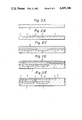
- FIG. 1A illustrates the principal sectional view of a semiconductor device in accordance with an embodiment of the present invention
- FIGS. 1B and 1C illustrate respectively the principal sectional views of semiconductor devices in accordance with other embodiments of the present invention.
- FIGS. 2A through 2K illustrate the sectional views of the semiconductor device of FIG. 1A in various process steps in the method of manufacturing the semiconductor device in accordance with the present invention.
- FIG. 1A The principal sectional view of a semiconductor device in accordance with an embodiment of the present invention is illustrated in FIG. 1A.
- an n-type epitaxially grown layer 5 is formed upon the p-type silicon substrate 1, and in the epitaxial layer 5 an npn type bipolar transistor I, an n-channel MOS FET II, and a p-channel MOS FET III that is, a C MOS FETs are constructed.
- FIGS. 2A through 2K The process steps of manufacturing the semiconductor device are illustrated in FIGS. 2A through 2K in sequence.
- FIG. 2A a p-type single crystal silicon substrate 1 oriented in the (100) plane with a resistivity of 10 to 20 ⁇ -cm is illustrated.
- n + -type islands 2' are formed by using an ordinary method of a selective diffusion, and then a p + -type region 3' for forming an isolation region and a p + -type island 4' for forming a p-well are formed as illustrated in FIG. 2B.
- a p-type epitaxial layer 5 with a resistivity of 4 to 5 ⁇ -cm is grown up to about 10 ⁇ m in thickness.
- the n-type and p-type regions 2', 3' and 4' are buried into the epitaxial layer 5 and form buried layers 2, 3 and 4 as illustrated in FIG. 2C.
- a p-type island 6 for the formation of a p-well and a n + -type island 7 for the formation of a collector-leading region are formed on the surface of the epitaxial layer 5, and then by the thermal oxidation of the surface of the epitaxial layer 5, a silicon dioxide (SiO 2 ) film, that is, an insulating film 8, is formed as shown in FIG. 2D.
- SiO 2 silicon dioxide
- a p-type isolation 9 and a p-well 11 are formed by carrying out a drive-in process.
- the n-type collector contact region 12 is formed as illustrated in FIG. 2E.
- the region I surrounded by the isolation area 9 is the region for forming the npn type transistor
- the region II divided by the isolation area 9 and the p-well 11 is the region for forming the p channel MOS FET
- the region III defined by the p-well 11 is the region for forming the n channel MOS FET.
- the source and drain regions 13, 14 of the n channel MOS FET (n MOS) and the n-type channel stopper 15 of the p channel MOS FET (p MOS) are formed, as illustrated in FIG. 2F.
- the base region 16 of the npn type transistor, the source and drain regions 17, 18 of the p MOS, and the p-type channel stopper 19 of the n MOS are formed, as illustrated in FIG. 2G.
- the SiO 2 film 8 at the positions for forming the gate regions of the p MOS and the n MOS is removed, and after further heating and oxidizing the exposed surface of the epitaxial layer, the gate oxide films 20, 20', with about 1000 ⁇ in thickness, are formed, as illustrated in FIG. 2H.
- the above-mentioned process step be carried out by using the hydrochloric acid oxidation method in which the oxidation is effected in an atmosphere containing a hydrochloric acid (HCl) gas.
- the substrate is annealed at a temperature of about 1100° C.
- a collector electrode window 21 is opened on the surface of the collector-leading region 12
- an emitter electrode window 22 and a base electrode window 23 are opened on the surface of the base region 16
- a source electrode window 24 and a drain electrode window 25 are opened respectively in the source and drain regions 17, 18 of the p MOS
- a source electrode window 26 and a drain electrode window 27 are opened respectively in the source and drain regions 13, 14 of the n MOS.
- an undoped polycrystal silicon layer 28 is formed upon all the surface of the substrate including its portions on the above-mentioned electrode windows 21 through 27 as illustrated in FIG. 2I.
- the thickness of the polycrystal silicon layer 28 is usually made about 2000 ⁇ . However this thickness may be made about 4000 ⁇ (thicker than 2000 ⁇ ) in order to gain a so-called silicon gate characteristic, or it may be made 500 ⁇ (thinner than 2000 ⁇ ) in order to gain a so-called aluminum gate characteristic.
- the PSG film 29 is selectively removed at the positions of the base electrode window 23, and the source and drain electrode windows 24, 25 of the n MOS, to which positions the n-type impurity should not be introduced.
- the PSG film 29 selectively removed by using a conventional photolithography technique.
- the n-type impurity phosphorus (P) is diffused from the remaining PSG film 29 through the polycrystal silicon layer 28 into the surface of the epitaxial layer at positions under the collector electrode window 21, the emitter electrode window 22, and the source and drain electrode windows 26, 27 of the n MOS.
- a collector contact layer 30, an emitter region 31, a source contact layer 32 and a drain contact layer 33 of the n MOS, all of which are of a high impurity concentration n-type, are formed as illustrated in FIG. 2J. Then, the remaining areas of the PSG layer 29 are all removed by using an etching solution.
- the phosphorus (P) is introduced into the area of the polycrystal silicon layer 28 directly under the PSG film 29 so that this area becomes n-type, while into the areas of the polycrystal silicon layer 28 of the base electrode window 23, the source and drain electrode windows 24, 25 of the p MOS, which make contact directly with the p-type regions, the p-type impurity contained in these p-type regions is diffused so that these areas of the polycrystal silicon layer become p-type.
- the areas of the polycrystal silicon layer 28 in contact with the respective regions through the respective electrode windows 21 through 27, have the same conductivity type as those of the corresponding underlying regions, and these areas are connected favorably by ohmic contact with their corresponding regions and can be used for the electrode contacts of these regions as they are.
- an aluminum (Al) layer is formed to cover the polycrystal silicon layer 28, and the aluminum layer and the polycrystal silicon layer 28 under the aluminum layer are selectively removed to form a desired conductor wiring pattern, so that electrodes 34 though 42 composed of Al are formed, and finally the semiconductor device of FIG. 1A according to the present invention is obtained as illustrated in FIG. 2K.
- the polycrystal silicon layer is coated; furthermore the PSG layer is coated over the electrode windows of the n-type regions, and by carrying out a so-called diffusion of impurity through the polysilicon method, in which the PSG layer is used as a source of impurity and the polycrystal silicon layer is used as a medium of impurity diffusion, the n-type impurity is diffused through only the desired electrode windows.
- the polycrystal silicon layer can be used as a protection film and therefore the thickness of the gate oxide film is kept unchanged during the above-mentioned diffusion of impurity through polysilicon. Furthermore, in the case of removing the PSG layer, the polycrystal silicon layer also serves as a protection film so that the thickness of the gate oxide film is kept unchanged. Accordingly, in the above-mentioned semiconductor device, the current amplification factor h FE of the bipolar transistor and the threshold voltages V TH of the p MOS and n MOS can be controlled independently.
- the Al electrodes of all the regions are attached to the surface of the regions through the polycrystal silicon layer which are connected favorably in ohmic contact with the surface so that, so-called Al immersion which would otherwise be caused by an excessive alloying with the substrate silicon, is prevented. Therefore no pn junction near the surface is destroyed.
- the method of manufacturing a semiconductor device according to the present invention is not limited by one embodiment described above, and may be executed in various modifications.
- the thickness of the polycrystal silicon layer 28 may be as thin as 500 ⁇ , and over the gate insulating film the polycrystal silicon layer 28 may be reacted with the Al layer upon the layer 28 so that an Al gate MOS characteristics may be obtained.
- the semiconductor device obtained finally is that illustrated in FIG. 1B.
- the thickness of the polycrystal silicon layer may be as thick as 4000 ⁇ , and finally the Al layer on the polycrystal silicon layer may be removed to form a silicon gate. In this case, a semiconductor device as illustrated in FIG. 1C is obtained.
- a photo resist film which covers all the area of the surface except the portion on which the PSG layer 29 has been coated, is formed (refer to FIG. 2J).
- the photo resist film is used as a mask and an n-type impurity such as phosphorus (P) is implanted into the exposed polycrystal silicon layer and into the epitaxial layer under it by the ion implantation method. Then the photo resist film is removed and the substrate is annealed.
- a SiO 2 film is formed instead of the photo resist film of the above-mentioned method and the n-type impurity is introduced by the selective diffusion method using the SiO 2 film as a mask.
- the method of manufacturing a semiconductor device according to the present invention can be applicable to any combination of a bipolar transistor and a MIS FET other than that of a npn transistor and a C MOS, as illustrated in FIG. 1A, for example that of a pnp transistor and a C MOS.
- the emitter region of the bipolar transistor and the gate insulating film can be formed as desired by a simple manufacturing process without their having a mutual bad influence on each other. Therefore, there can be provided a semiconductor device in which the current amplification factor h FE of the bipolar transistor and the threshold voltage V TH of the MIS FET can be controlled independently, and also there is provided a method of manufacturing it.
Landscapes
- Engineering & Computer Science (AREA)
- Physics & Mathematics (AREA)
- Condensed Matter Physics & Semiconductors (AREA)
- General Physics & Mathematics (AREA)
- Computer Hardware Design (AREA)
- Microelectronics & Electronic Packaging (AREA)
- Power Engineering (AREA)
- Manufacturing & Machinery (AREA)
- Bipolar Transistors (AREA)
- Metal-Oxide And Bipolar Metal-Oxide Semiconductor Integrated Circuits (AREA)
Abstract
Description
Claims (4)
Applications Claiming Priority (2)
| Application Number | Priority Date | Filing Date | Title |
|---|---|---|---|
| JP55151557A JPS5775453A (en) | 1980-10-29 | 1980-10-29 | Semiconductor device and manufacture thereof |
| JP55-151557 | 1980-10-29 |
Publications (1)
| Publication Number | Publication Date |
|---|---|
| US4497106A true US4497106A (en) | 1985-02-05 |
Family
ID=15521122
Family Applications (1)
| Application Number | Title | Priority Date | Filing Date |
|---|---|---|---|
| US06/315,903 Expired - Lifetime US4497106A (en) | 1980-10-29 | 1981-10-28 | Semiconductor device and a method of manufacturing the same |
Country Status (4)
| Country | Link |
|---|---|
| US (1) | US4497106A (en) |
| EP (1) | EP0052450B1 (en) |
| JP (1) | JPS5775453A (en) |
| DE (1) | DE3171338D1 (en) |
Cited By (33)
| Publication number | Priority date | Publication date | Assignee | Title |
|---|---|---|---|---|
| US4569123A (en) * | 1983-09-09 | 1986-02-11 | Kabushiki Kaisha Toshiba | Method of manufacturing a semiconductor device utilizing simultaneous diffusion from an ion implanted polysilicon layer |
| US4724221A (en) * | 1981-10-28 | 1988-02-09 | U.S. Philips Corporation | High-speed, low-power-dissipation integrated circuits |
| US4806499A (en) * | 1985-06-13 | 1989-02-21 | Oki Electric Industry Co., Ltd. | Method of manufacturing Bi-CMOS semiconductor IC devices using dopant rediffusion |
| US4814288A (en) * | 1986-07-14 | 1989-03-21 | Hitachi, Ltd. | Method of fabricating semiconductor devices which include vertical elements and control elements |
| US4818720A (en) * | 1983-10-07 | 1989-04-04 | Kabushiki Kaisha Toshiba | Method for manufacturing a BiCMOS device |
| US4859630A (en) * | 1986-03-26 | 1989-08-22 | U.S. Philips Corporation | Method of manufacturing a semiconductor device |
| US4960726A (en) * | 1989-10-19 | 1990-10-02 | International Business Machines Corporation | BiCMOS process |
| US4970174A (en) * | 1987-09-15 | 1990-11-13 | Samsung Electronics Co., Ltd. | Method for making a BiCMOS semiconductor device |
| US4980303A (en) * | 1987-08-19 | 1990-12-25 | Fujitsu Limited | Manufacturing method of a Bi-MIS semiconductor device |
| US4994887A (en) * | 1987-11-13 | 1991-02-19 | Texas Instruments Incorporated | High voltage merged bipolar/CMOS technology |
| US5001081A (en) * | 1988-01-19 | 1991-03-19 | National Semiconductor Corp. | Method of manufacturing a polysilicon emitter and a polysilicon gate using the same etch of polysilicon on a thin gate oxide |
| US5008208A (en) * | 1988-12-07 | 1991-04-16 | Honeywell Inc. | Method of making planarized, self-aligned bipolar integrated circuits |
| US5013677A (en) * | 1989-06-19 | 1991-05-07 | Sony Corporation | Method for manufacture of semiconductor device |
| US5013678A (en) * | 1986-11-18 | 1991-05-07 | Siemens Aktiengesellschaft | Method of making an integrated circuit comprising load resistors arranged on the field oxide zones which separate the active transistor zones |
| US5030588A (en) * | 1988-04-05 | 1991-07-09 | Seiko Instruments Inc. | Method of making semiconductor device with film resistor |
| US5082796A (en) * | 1990-07-24 | 1992-01-21 | National Semiconductor Corporation | Use of polysilicon layer for local interconnect in a CMOS or BiCMOS technology incorporating sidewall spacers |
| US5100824A (en) * | 1985-04-01 | 1992-03-31 | National Semiconductor Corporation | Method of making small contactless RAM cell |
| US5124817A (en) * | 1988-01-19 | 1992-06-23 | National Semiconductor Corporation | Polysilicon emitter and a polysilicon gate using the same etch of polysilicon on a thin gate oxide |
| US5160985A (en) * | 1989-01-06 | 1992-11-03 | Mitsubishi Denki Kabushiki Kaisha | Insulated gate bipolar transistor |
| US5179031A (en) * | 1988-01-19 | 1993-01-12 | National Semiconductor Corporation | Method of manufacturing a polysilicon emitter and a polysilicon gate using the same etch of polysilicon on a thin gate oxide |
| US5280188A (en) * | 1985-03-07 | 1994-01-18 | Kabushiki Kaisha Toshiba | Method of manufacturing a semiconductor integrated circuit device having at least one bipolar transistor and a plurality of MOS transistors |
| US5340762A (en) * | 1985-04-01 | 1994-08-23 | Fairchild Semiconductor Corporation | Method of making small contactless RAM cell |
| WO1995030897A1 (en) * | 1994-05-09 | 1995-11-16 | Olin Corporation | Broad range moisture analyzer and method |
| US5484739A (en) * | 1993-12-17 | 1996-01-16 | Samsung Electronics Co., Ltd. | Method for manufacturing a CMOS semiconductor device |
| US5508549A (en) * | 1982-11-24 | 1996-04-16 | Hitachi, Ltd. | Semiconductor integrated circuit device and a method for manufacturing the same |
| US5556796A (en) * | 1995-04-25 | 1996-09-17 | Micrel, Inc. | Self-alignment technique for forming junction isolation and wells |
| US5668037A (en) * | 1995-10-06 | 1997-09-16 | Micron Technology, Inc. | Method of forming a resistor and integrated circuitry having a resistor construction |
| US5736447A (en) * | 1994-06-13 | 1998-04-07 | Samsung Electronics Co., Ltd. | Method for manufacturing a bipolar junction transistor having a polysilicon emitter |
| US5923078A (en) * | 1996-07-11 | 1999-07-13 | Micron Technology, Inc. | Method of forming a resistor and integrated circuitry having a resistor construction |
| US6130137A (en) * | 1997-10-20 | 2000-10-10 | Micron Technology, Inc. | Method of forming a resistor and integrated circuitry having a resistor construction |
| US6208010B1 (en) * | 1985-09-25 | 2001-03-27 | Hitachi, Ltd. | Semiconductor memory device |
| US6218253B1 (en) * | 1996-02-28 | 2001-04-17 | Nec Corporation | Method of manufacturing a bipolar transistor by using only two mask layers |
| US20030178699A1 (en) * | 1985-09-25 | 2003-09-25 | Shinji Nakazato | Semiconductor memory device |
Families Citing this family (16)
| Publication number | Priority date | Publication date | Assignee | Title |
|---|---|---|---|---|
| JPS58225663A (en) * | 1982-06-23 | 1983-12-27 | Toshiba Corp | Manufacturing method of semiconductor device |
| DE3230077A1 (en) * | 1982-08-12 | 1984-02-16 | Siemens AG, 1000 Berlin und 8000 München | SEMICONDUCTOR CIRCUIT CONTAINING INTEGRATED BIPOLAR AND MOS TRANSISTORS ON A CHIP AND METHOD FOR THEIR PRODUCTION |
| JPS5931052A (en) * | 1982-08-13 | 1984-02-18 | Hitachi Ltd | Method for manufacturing semiconductor integrated circuit device |
| JPS5955052A (en) * | 1982-09-24 | 1984-03-29 | Hitachi Ltd | Semiconductor integrated circuit device and manufacture thereof |
| JPS5987850A (en) * | 1982-11-11 | 1984-05-21 | Matsushita Electronics Corp | semiconductor equipment |
| DE3369030D1 (en) * | 1983-04-18 | 1987-02-12 | Itt Ind Gmbh Deutsche | Method of making a monolithic integrated circuit comprising at least one insulated gate field-effect transistor |
| GB2143083B (en) * | 1983-07-06 | 1987-11-25 | Standard Telephones Cables Ltd | Semiconductor structures |
| JPS60158655A (en) * | 1984-01-27 | 1985-08-20 | Rohm Co Ltd | Semiconductor device and its manufacturing method |
| JPH0691197B2 (en) * | 1984-02-08 | 1994-11-14 | 株式会社日立製作所 | Semiconductor integrated circuit device |
| CA1258320A (en) * | 1985-04-01 | 1989-08-08 | Madhukar B. Vora | Small contactless ram cell |
| GB2193036B (en) * | 1986-07-24 | 1990-05-02 | Mitsubishi Electric Corp | Method of fabricating a semiconductor integrated circuit device |
| JP2538600B2 (en) * | 1987-07-23 | 1996-09-25 | 富士通株式会社 | Method for manufacturing semiconductor device |
| US5121185A (en) * | 1987-10-09 | 1992-06-09 | Hitachi, Ltd. | Monolithic semiconductor IC device including blocks having different functions with different breakdown voltages |
| DE3914910C2 (en) * | 1988-05-10 | 1999-11-25 | Northern Telecom Ltd | Method of making an integrated circuit |
| GB8810973D0 (en) * | 1988-05-10 | 1988-06-15 | Stc Plc | Improvements in integrated circuits |
| JPH04237160A (en) * | 1991-01-22 | 1992-08-25 | Nec Corp | Bipolar cmos composite type semiconductor device |
Citations (5)
| Publication number | Priority date | Publication date | Assignee | Title |
|---|---|---|---|---|
| JPS51148380A (en) * | 1975-06-14 | 1976-12-20 | Fujitsu Ltd | Manufacturing method of electric field semiconductor device |
| US4120707A (en) * | 1977-03-30 | 1978-10-17 | Harris Corporation | Process of fabricating junction isolated IGFET and bipolar transistor integrated circuit by diffusion |
| US4125426A (en) * | 1975-04-29 | 1978-11-14 | Fujitsu Limited | Method of manufacturing semiconductor device |
| GB2011173A (en) * | 1977-12-21 | 1979-07-04 | Tokyo Shibaura Electric Co | Semiconductor device and method of producing the same |
| US4233615A (en) * | 1977-08-25 | 1980-11-11 | Matsushita Electric Industrial Co., Ltd. | Semiconductor integrated circuit device |
-
1980
- 1980-10-29 JP JP55151557A patent/JPS5775453A/en active Pending
-
1981
- 1981-10-28 US US06/315,903 patent/US4497106A/en not_active Expired - Lifetime
- 1981-10-29 DE DE8181305120T patent/DE3171338D1/en not_active Expired
- 1981-10-29 EP EP81305120A patent/EP0052450B1/en not_active Expired
Patent Citations (5)
| Publication number | Priority date | Publication date | Assignee | Title |
|---|---|---|---|---|
| US4125426A (en) * | 1975-04-29 | 1978-11-14 | Fujitsu Limited | Method of manufacturing semiconductor device |
| JPS51148380A (en) * | 1975-06-14 | 1976-12-20 | Fujitsu Ltd | Manufacturing method of electric field semiconductor device |
| US4120707A (en) * | 1977-03-30 | 1978-10-17 | Harris Corporation | Process of fabricating junction isolated IGFET and bipolar transistor integrated circuit by diffusion |
| US4233615A (en) * | 1977-08-25 | 1980-11-11 | Matsushita Electric Industrial Co., Ltd. | Semiconductor integrated circuit device |
| GB2011173A (en) * | 1977-12-21 | 1979-07-04 | Tokyo Shibaura Electric Co | Semiconductor device and method of producing the same |
Non-Patent Citations (4)
| Title |
|---|
| IBM Technical Disclosure Bulletin, "NPN N-Channel Bipolar FET Devices", vol. 17, No. 10, Mar. 1975, pp. 2935-2936. |
| IBM Technical Disclosure Bulletin, NPN N Channel Bipolar FET Devices , vol. 17, No. 10, Mar. 1975, pp. 2935 2936. * |
| Patent Abstracts of Japan, vol. 5, No. 55, Apr. 16, 1981, (JP A 56 007462). * |
| Patent Abstracts of Japan, vol. 5, No. 55, Apr. 16, 1981, (JP-A-56-007462). |
Cited By (41)
| Publication number | Priority date | Publication date | Assignee | Title |
|---|---|---|---|---|
| US4724221A (en) * | 1981-10-28 | 1988-02-09 | U.S. Philips Corporation | High-speed, low-power-dissipation integrated circuits |
| US5508549A (en) * | 1982-11-24 | 1996-04-16 | Hitachi, Ltd. | Semiconductor integrated circuit device and a method for manufacturing the same |
| US4569123A (en) * | 1983-09-09 | 1986-02-11 | Kabushiki Kaisha Toshiba | Method of manufacturing a semiconductor device utilizing simultaneous diffusion from an ion implanted polysilicon layer |
| US4818720A (en) * | 1983-10-07 | 1989-04-04 | Kabushiki Kaisha Toshiba | Method for manufacturing a BiCMOS device |
| US4965220A (en) * | 1983-10-07 | 1990-10-23 | Kabushiki Kaisha Toshiba | Method of manufacturing a semiconductor integrated circuit device comprising an MOS transistor and a bipolar transistor |
| US5280188A (en) * | 1985-03-07 | 1994-01-18 | Kabushiki Kaisha Toshiba | Method of manufacturing a semiconductor integrated circuit device having at least one bipolar transistor and a plurality of MOS transistors |
| US5100824A (en) * | 1985-04-01 | 1992-03-31 | National Semiconductor Corporation | Method of making small contactless RAM cell |
| US5340762A (en) * | 1985-04-01 | 1994-08-23 | Fairchild Semiconductor Corporation | Method of making small contactless RAM cell |
| US4806499A (en) * | 1985-06-13 | 1989-02-21 | Oki Electric Industry Co., Ltd. | Method of manufacturing Bi-CMOS semiconductor IC devices using dopant rediffusion |
| US20030178699A1 (en) * | 1985-09-25 | 2003-09-25 | Shinji Nakazato | Semiconductor memory device |
| US6740958B2 (en) | 1985-09-25 | 2004-05-25 | Renesas Technology Corp. | Semiconductor memory device |
| US6208010B1 (en) * | 1985-09-25 | 2001-03-27 | Hitachi, Ltd. | Semiconductor memory device |
| US6864559B2 (en) | 1985-09-25 | 2005-03-08 | Renesas Technology Corp. | Semiconductor memory device |
| US4859630A (en) * | 1986-03-26 | 1989-08-22 | U.S. Philips Corporation | Method of manufacturing a semiconductor device |
| US4814288A (en) * | 1986-07-14 | 1989-03-21 | Hitachi, Ltd. | Method of fabricating semiconductor devices which include vertical elements and control elements |
| US5013678A (en) * | 1986-11-18 | 1991-05-07 | Siemens Aktiengesellschaft | Method of making an integrated circuit comprising load resistors arranged on the field oxide zones which separate the active transistor zones |
| US4980303A (en) * | 1987-08-19 | 1990-12-25 | Fujitsu Limited | Manufacturing method of a Bi-MIS semiconductor device |
| US4970174A (en) * | 1987-09-15 | 1990-11-13 | Samsung Electronics Co., Ltd. | Method for making a BiCMOS semiconductor device |
| US4994887A (en) * | 1987-11-13 | 1991-02-19 | Texas Instruments Incorporated | High voltage merged bipolar/CMOS technology |
| US5179031A (en) * | 1988-01-19 | 1993-01-12 | National Semiconductor Corporation | Method of manufacturing a polysilicon emitter and a polysilicon gate using the same etch of polysilicon on a thin gate oxide |
| US5124817A (en) * | 1988-01-19 | 1992-06-23 | National Semiconductor Corporation | Polysilicon emitter and a polysilicon gate using the same etch of polysilicon on a thin gate oxide |
| US5001081A (en) * | 1988-01-19 | 1991-03-19 | National Semiconductor Corp. | Method of manufacturing a polysilicon emitter and a polysilicon gate using the same etch of polysilicon on a thin gate oxide |
| US5030588A (en) * | 1988-04-05 | 1991-07-09 | Seiko Instruments Inc. | Method of making semiconductor device with film resistor |
| US5008208A (en) * | 1988-12-07 | 1991-04-16 | Honeywell Inc. | Method of making planarized, self-aligned bipolar integrated circuits |
| US5160985A (en) * | 1989-01-06 | 1992-11-03 | Mitsubishi Denki Kabushiki Kaisha | Insulated gate bipolar transistor |
| US5013677A (en) * | 1989-06-19 | 1991-05-07 | Sony Corporation | Method for manufacture of semiconductor device |
| US4960726A (en) * | 1989-10-19 | 1990-10-02 | International Business Machines Corporation | BiCMOS process |
| US5082796A (en) * | 1990-07-24 | 1992-01-21 | National Semiconductor Corporation | Use of polysilicon layer for local interconnect in a CMOS or BiCMOS technology incorporating sidewall spacers |
| US5484739A (en) * | 1993-12-17 | 1996-01-16 | Samsung Electronics Co., Ltd. | Method for manufacturing a CMOS semiconductor device |
| WO1995030897A1 (en) * | 1994-05-09 | 1995-11-16 | Olin Corporation | Broad range moisture analyzer and method |
| US5736447A (en) * | 1994-06-13 | 1998-04-07 | Samsung Electronics Co., Ltd. | Method for manufacturing a bipolar junction transistor having a polysilicon emitter |
| WO1996036067A3 (en) * | 1995-04-25 | 1997-01-16 | Micrel Inc | Self-alignment technique for junction isolation and wells |
| WO1996036067A2 (en) * | 1995-04-25 | 1996-11-14 | Micrel, Incorporated | Self-alignment technique for junction isolation and wells |
| US5556796A (en) * | 1995-04-25 | 1996-09-17 | Micrel, Inc. | Self-alignment technique for forming junction isolation and wells |
| US5780920A (en) * | 1995-10-06 | 1998-07-14 | Micron Technology, Inc. | Method of forming a resistor and integrated circuitry having a resistor construction |
| US5821150A (en) * | 1995-10-06 | 1998-10-13 | Micron Technology, Inc. | Method of forming a resistor and integrated circuitry having a resistor construction |
| US5940712A (en) * | 1995-10-06 | 1999-08-17 | Micron Technology, Inc. | Method of forming a resistor and integrated circuitry having a resistor construction |
| US5668037A (en) * | 1995-10-06 | 1997-09-16 | Micron Technology, Inc. | Method of forming a resistor and integrated circuitry having a resistor construction |
| US6218253B1 (en) * | 1996-02-28 | 2001-04-17 | Nec Corporation | Method of manufacturing a bipolar transistor by using only two mask layers |
| US5923078A (en) * | 1996-07-11 | 1999-07-13 | Micron Technology, Inc. | Method of forming a resistor and integrated circuitry having a resistor construction |
| US6130137A (en) * | 1997-10-20 | 2000-10-10 | Micron Technology, Inc. | Method of forming a resistor and integrated circuitry having a resistor construction |
Also Published As
| Publication number | Publication date |
|---|---|
| JPS5775453A (en) | 1982-05-12 |
| DE3171338D1 (en) | 1985-08-14 |
| EP0052450B1 (en) | 1985-07-10 |
| EP0052450A1 (en) | 1982-05-26 |
Similar Documents
| Publication | Publication Date | Title |
|---|---|---|
| US4497106A (en) | Semiconductor device and a method of manufacturing the same | |
| US5065208A (en) | Integrated bipolar and CMOS transistor with titanium nitride interconnections | |
| US4486942A (en) | Method of manufacturing semiconductor integrated circuit BI-MOS device | |
| US3909320A (en) | Method for forming MOS structure using double diffusion | |
| EP0110313B1 (en) | Semiconductor integrated circuit device and a method for manufacturing the same | |
| US4346512A (en) | Integrated circuit manufacturing method | |
| GB1567197A (en) | Methods of manufacturing semiconductor devices | |
| US5019523A (en) | Process for making polysilicon contacts to IC mesas | |
| EP0278619B1 (en) | Integrated bipolar and CMOS transistor fabrication process | |
| US4353085A (en) | Integrated semiconductor device having insulated gate field effect transistors with a buried insulating film | |
| KR910006672B1 (en) | Semiconductor integrated circuit device and manufacturing method thereof | |
| US4507846A (en) | Method for making complementary MOS semiconductor devices | |
| EP0183624A2 (en) | L-fast fabrication process for high speed bipolar analog large scale integrated circuits | |
| US4965216A (en) | Method of fabricating a bi-CMOS device | |
| US4277882A (en) | Method of producing a metal-semiconductor field-effect transistor | |
| US5242849A (en) | Method for the fabrication of MOS devices | |
| EP0030147A1 (en) | Method for manufacturing a semiconductor integrated circuit | |
| US4426766A (en) | Method of fabricating high density high breakdown voltage CMOS devices | |
| EP0337823A2 (en) | MOS field effect transistor having high breakdown voltage | |
| JPS5843912B2 (en) | Method for manufacturing semiconductor integrated circuit device | |
| US4722912A (en) | Method of forming a semiconductor structure | |
| EP0405063A2 (en) | An insulated-gate fet on an soi-structure | |
| US4528581A (en) | High density CMOS devices with conductively interconnected wells | |
| JPH0239091B2 (en) | ||
| JP2910369B2 (en) | Manufacturing method of floating gate type semiconductor memory device |
Legal Events
| Date | Code | Title | Description |
|---|---|---|---|
| AS | Assignment |
Owner name: FUJITSU LIMITED 1015 KAMIKODANAKA NAKAHARA-KU KAWA Free format text: ASSIGNMENT OF ASSIGNORS INTEREST.;ASSIGNORS:MOMMA, YOSHINOBU;FUNATSU, TSUNEO;SASAKI, ATUSI;REEL/FRAME:003941/0692 Effective date: 19811016 |
|
| STCF | Information on status: patent grant |
Free format text: PATENTED CASE |
|
| FPAY | Fee payment |
Year of fee payment: 4 |
|
| FEPP | Fee payment procedure |
Free format text: PAYOR NUMBER ASSIGNED (ORIGINAL EVENT CODE: ASPN); ENTITY STATUS OF PATENT OWNER: LARGE ENTITY |
|
| FPAY | Fee payment |
Year of fee payment: 8 |
|
| FEPP | Fee payment procedure |
Free format text: PAYOR NUMBER ASSIGNED (ORIGINAL EVENT CODE: ASPN); ENTITY STATUS OF PATENT OWNER: LARGE ENTITY |
|
| FPAY | Fee payment |
Year of fee payment: 12 |