US4463273A - Electronic circuits and structures employing enhancement and depletion type IGFETs - Google Patents
Electronic circuits and structures employing enhancement and depletion type IGFETs Download PDFInfo
- Publication number
- US4463273A US4463273A US06/314,849 US31484981A US4463273A US 4463273 A US4463273 A US 4463273A US 31484981 A US31484981 A US 31484981A US 4463273 A US4463273 A US 4463273A
- Authority
- US
- United States
- Prior art keywords
- igfet
- source
- conductivity type
- transistor
- conduction path
- Prior art date
- Legal status (The legal status is an assumption and is not a legal conclusion. Google has not performed a legal analysis and makes no representation as to the accuracy of the status listed.)
- Expired - Lifetime
Links
Images


Classifications
-
- H—ELECTRICITY
- H03—ELECTRONIC CIRCUITRY
- H03K—PULSE TECHNIQUE
- H03K19/00—Logic circuits, i.e. having at least two inputs acting on one output; Inverting circuits
- H03K19/02—Logic circuits, i.e. having at least two inputs acting on one output; Inverting circuits using specified components
- H03K19/08—Logic circuits, i.e. having at least two inputs acting on one output; Inverting circuits using specified components using semiconductor devices
- H03K19/094—Logic circuits, i.e. having at least two inputs acting on one output; Inverting circuits using specified components using semiconductor devices using field-effect transistors
- H03K19/096—Synchronous circuits, i.e. using clock signals
- H03K19/0963—Synchronous circuits, i.e. using clock signals using transistors of complementary type
-
- H—ELECTRICITY
- H03—ELECTRONIC CIRCUITRY
- H03K—PULSE TECHNIQUE
- H03K19/00—Logic circuits, i.e. having at least two inputs acting on one output; Inverting circuits
- H03K19/02—Logic circuits, i.e. having at least two inputs acting on one output; Inverting circuits using specified components
- H03K19/08—Logic circuits, i.e. having at least two inputs acting on one output; Inverting circuits using specified components using semiconductor devices
- H03K19/094—Logic circuits, i.e. having at least two inputs acting on one output; Inverting circuits using specified components using semiconductor devices using field-effect transistors
- H03K19/0944—Logic circuits, i.e. having at least two inputs acting on one output; Inverting circuits using specified components using semiconductor devices using field-effect transistors using MOSFET or insulated gate field-effect transistors, i.e. IGFET
- H03K19/0948—Logic circuits, i.e. having at least two inputs acting on one output; Inverting circuits using specified components using semiconductor devices using field-effect transistors using MOSFET or insulated gate field-effect transistors, i.e. IGFET using CMOS or complementary insulated gate field-effect transistors
- H03K19/09482—Logic circuits, i.e. having at least two inputs acting on one output; Inverting circuits using specified components using semiconductor devices using field-effect transistors using MOSFET or insulated gate field-effect transistors, i.e. IGFET using CMOS or complementary insulated gate field-effect transistors using a combination of enhancement and depletion transistors
- H03K19/09485—Logic circuits, i.e. having at least two inputs acting on one output; Inverting circuits using specified components using semiconductor devices using field-effect transistors using MOSFET or insulated gate field-effect transistors, i.e. IGFET using CMOS or complementary insulated gate field-effect transistors using a combination of enhancement and depletion transistors with active depletion transistors
Definitions
- This invention relates to inverters employing insulated-gate, field-effect transistors (IGFETs).
- IGFETs insulated-gate, field-effect transistors
- a single transistor transmission gate often is used to selectively couple signals from one circuit to another.
- the gating transistor operates in the grounded mode--i.e., common source or common emitter--for one value of input signal and in the follower mode--i.e., as a source follower or emitter follower--for another value of input signal, and this can cause problems.
- the voltage transmitted to the receiving point does not reach the full value of the sending voltage because of the threshold characteristic of the gating transistor.
- this mode there is a voltage offset (V T or V BE ) between the control electrode (gate or base) of the transistor and one end of its conduction path and this same offset appears across the conduction path of the transistor.
- V T threshold voltage
- the voltage actually transmitted to the receiving point may be insufficient to trigger (or turn-off) a circuit or element connected at the receiving point.
- Another solution is to overdrive the transmission gate by pulses having an amplitude equal to at least the sum of the signal and threshold voltage. Overdriving the gate transistor is not feasible in all instances and, in practice, may require more than one power supply to generate control signals of large amplitude. Moreover, overdriving increases the power consumption and the noise level in the circuit and these are serious disadvantages.
- One aspect of the present invention involves the use of a controllable impedance means connected in series with the conduction path of transistors forming a complementary inverter for selectively "skewing" the inverter in a direction to center its toggle point with respect to the signals applied to the inverter input.
- the "skewed” inverter is thereby compensated for offsets or asymmetry in its input signals.
- skewed inverters are used to form memory cells which can be easily placed in either binary condition.
- Still another aspect of the invention is the use of the controllable impedances as "cross-unders” to enable the fabrication of "skewable” inverters requiring very little space.
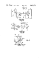
- FIGS. 1A and 1B are schematic diagrams of prior art transmission gate circuits
- FIGS. 2A and 2B are schematic diagrams of circuits embodying the invention.
- FIG. 3 is a drawing of the transfer characteristics of inverter circuits embodying the invention.
- FIGS. 4A and 4B are schematic diagrams of memory cell circuits embodying the invention.
- FIG. 5 is a schematic drawing of another memory cell circuit embodying the invention.
- FIG. 6 is a top view of a portion of an integrated circuit including a memory cell of the type shown in FIG. 5;
- FIG. 7 is a cross section of the portion of the integrated circuit shown in FIG. 6 taken along the line 7--7 of FIG. 6;
- FIG. 8 is a cross section of the position of the integrated circuit shown in FIG. 6 taken along the line 8--8 of FIG. 6.
- IGFETs insulated-gate field-effect transistors
- enhancement IGFETs of P conductivity type are identified by the letter P followed by a particular reference numeral
- depletion IGFETs of P conductivity type are identified by the letters PD.
- IGFETs of P conductivity type are also identified by an arrow pointing towards the body of the transistor.
- Enhancement IGFETs of N conductivity type are identified by the letter N followed by a particular reference numeral while depletion IGFETs are identified by the letters ND.
- Each IGFET of N conductivity type is also identified by an arrow pointing away from the body of the transistor.
- the IGFETs used have first and second electrodes which define the ends of a conduction path and a control electrode (gate) whose applied potential determines the conductivity of the conduction path.
- the first and second electrodes of an IGFET are referred to as the source and drain electrodes.
- the source electrode is defined as that one of the first and second electrodes having the more positive (higher) potential applied thereto.
- the source electrode is defined as that one of the first and second electrodes having the less positive (lower) potential applied thereto.
- V GS gate-to-source potential
- V T threshold voltage
- Conduction exists even with zero gate-to-source potential. Conduction may be increased by applying a forward bias between the gate and source or may be decreased (and eventually stopped) by applying a substantial reverse bias between the gate and source electrodes.
- IGFETs are bidirectional in the sense that when an enabling signal is applied to the control electrode, current can flow in either direction in the conduction path between the first and second electrodes, i.e. the source and drain are interchangeable.
- V S the voltage at the source electrode
- V G the threshold voltage of the device
- FIG. 1A shows a known transmission gate arrangement.
- An input or sending source represented by box 10 produces signals at its output terminal 12 by means of a switch S1 having a switch arm which may be connected either to a terminal 16 which is connected directly to ground or to a terminal 18 to which is applied a potential of +V volts.
- a switch arm is at terminal 18, the voltage (V 12 ) at sending point 12 is +V volts and if the switch arm is at terminal 16, V 12 is 0 volt.
- a transmission gate comprising a P-type field-effect transistor P3 has its conduction path, whose ends are defined by electrodes 34 and 36, connected between sending terminal 12 and receiving terminal 24.
- the gate electrode 38 of P3 is connected to a terminal 40, to which is applied a control signal (V C ) having a potential of either zero volts or +V volts.
- V C control signal
- Transistor P3 is turned-off (disabled) when V C is at +V volts, and is turned-on (enabled) when V C is lower than the potential at its source electrode by an amount exceeding the V T of P3.
- a load 26 whose input impedance includes a (distributed or discrete) capacitor 28 is connected to the receiving terminal 24.
- the load 26 includes a complementary inverter I1 comprised of transistors N1 and P1.
- Transistors N1 and P1 have their drain electrodes connected in common to output point or node 30, their source electrodes connected to ground and +V, respectively, and their gate electrodes connected to input node 24.
- V 36 the initial voltage at electrode 36 is +V volts (capacitor 28 is fully charged).
- V 12 and V C are set to ground potential, and P3 now operates as a source follower, with electrode 36 functioning as the source electrode.
- V 24 When P3 is initially rendered conductive, V 24 is at +V volts and a differential of V volts exists between source electrode 36 and gate electrode 38. As capacitor 28 discharges, the potential difference between source (36) and gate (38) decreases, causing an increase in the impedance of the conduction channel of P3. When the capacitor 28 is discharged such that V 24 has a value equal to the V T of P3, P3 becomes non-conducting and the capacitor 28 discharges no further (except for leakage current). Thus, with the input grounded, V 24 remains at a potential level equal to V T .
- the receiving terminal 24 charges up to the value of the input (+V volts) but for the other direction of conduction the receiving terminal does not discharge to the value of the input (0 volt); i.e. terminal 24 remains charged up to V T volts where V T is the offset of the gating transistor.
- both P1 (which was to be turned-on) and N1 (which was intended to be turned-off) conduct at the same time.
- P1 and N1 thus provide a low impedance conduction path between +V and ground which results in a high level of power dissipation.
- the output level at output 30 is undefined being somewhere between +V volts and ground depending on the conduction level through P1 and N1 and the impedance ratio of P1 to N1.
- FIG. 2A illustrates an embodiment of the invention in which certain limitations and disadvantages associated with the use of a single gating transistor are avoided.
- the circuit of FIG. 2A includes input source 10 and gating transistor P3 which are connected, and perform, as in FIG. 1A. Also, the gate electrodes of P1 and N1 are connected to terminal 24 with the source of P1 being connected to +V and the drains of P1 and N1 being connected to output terminal 30 as in FIG. 1A.
- the circuit includes a controllable impedance comprising a depletion IGFET ND connected at its drain electrode to the source of N1, connected at its source electrode to ground, and having its gate electrode connected to the gate electrode of P3.
- P1, N1 and ND form an inverter I1A.
- ND functions as a controllable impedance which enables the toggle, quiescent, or switching point of inverter I1A to be selectively changed as discussed below.
- V Q The shape of the transfer curve and hence the switching point (V Q ) of a complementary inverter is dependent (among others) on the characteristics and impedances of the N and P transistors forming the inverter.
- Curve C represents the transfer characteristic of an inverter whose P and N IGFETs have equal impedances for the same value of gate to source voltage (V GS ).
- inverter I1A When ND in FIG. 2A has +V volts applied to its gate (with its source at zero volts) the ON impedance of its conduction path is very low. For this condition the source of N1 is returned to ground via a relatively low impedance path, and the transfer characteristic of inverter I1A may be assumed to be as shown in waveform C of FIG. 3.
- P3 when enabled, can charge terminal 24 to +V volts when V 12 is at +V volts, but P3 can only discharge terminal 24 to V T volts when V 12 is at zero volt.
- the boundary values (+V and V T ) of V 24 are asymmetrical with respect to +V and ground and with respect to the input signal at terminal 12. Whereas the range of voltage at node 12 is centered about V/2, the center value of V 24 (due to the V T offset of P3) is shifted to [V+V T ]/2.
- inverter I1A (responsive to the signal at node 24) is "skewed" by applying a control signal of 0 volt to the gate of ND when a signal is coupled via P3 to the input of I1A.
- This substantially increases the effective impedance of the conduction path between output terminal 30 and ground in comparison to the impedance of the conduction path between terminal 30 and +V but since ND is a depletion device it remains conducting.
- a depletion device can conduct even with a V GS of zero volt as in the present example.
- the impedance of its conduction path is substantially greater than when a forward bias (i.e.
- inverter I1A for the condition when the V GS of ND is zero is shown in curve A of FIG. 3. Indeed, the quiescent point (V QA ) of inverter I1A is significantly more positive than V/2.
- I1A is "skewed” such that its output will have one binary value (e.g. "low”) for signals at node 24 more positive than [V+V T ]/2 and its output will have the other binary value (e.g. "high”) for signals at node 24 less positive than [V+V T ]/2.
- Varying the impedance of ND as described above enhances the operation of the circuit of FIG. 2A briefly discussed below.
- the OFF impedance of P1 is several orders of magnitude greater than the impedance of ND with its V GS equal to zero volt.
- N1 and ND which are ON and conducting can discharge terminal 30 to ground and cause e 0 to be at or close to zero volts.
- N1 with its gate at V T volts and its source returned to via the realtively high impedance of ND to ground also presents a relatively high source-to-drain impedance.
- N1 and ND present a very high impedance between terminal 30 and ground allowing e 0 at terminal 30 to be very close to +V volts. Therefore, the output of I1A is well defined due to the role of ND and the power dissipation of the inverter is relatively small.
- the circuit of FIG. 2B includes input source 10 and gating transistor N3 which are connected and perform as in FIG. 1B. Also, the gate electrodes of transistors P1 and N1 are connected to terminal 24, with the source of N1 being connected to ground and the drains of P1 and N1 being connected to terminal 30 as in FIG. 1B. However, in this circuit the source-to-drain path of a P type depletion transistor PD is connected between the source of P1 and +V volts, and the gate electrode of PD is connected to the gate electrode of N3.
- the control signal V C which swings between 0 and +V volts is applied to the gate electrodes of N3 and P3.
- PD, P1 and N1 form inverter I1B.
- the addition of PD and the ability to alter its gate voltage enables the toggle or quiescent point of inverter I1B to be selectively changed.
- V C +V volts
- node 24 can be driven to ground when V 12 is grounded, but node 24 can only be changed to [+V-V T ] volts when V 12 is at +V volts. Therefore, with +V applied to the gate of N3 and with V 12 varying between 0 and +V volts, V 24 varies between 0 and [V-V T ] volts. To compensate for the V T offset at node 24 the quiescent point of inverter I1B is made settable to the mid range of the voltage at node 24; i.e., [V-V T ]/2.
- the addition of PD enables the quiescent point of inverter I1B to be shifted by controlling the potential applied to the gate of PD.
- PD When 0 volt is applied to the gate of PD, PD is turned-on hard and its source-to-drain impedance is very low whereby the source of P1 is coupled to +V via a very low impedance.
- the transfer characteristic of FIG. I1B may be assumed to be as shown in waveform C of FIG. 3.
- Increasing the impedance of PD increases the effective impedance between node 30 and +V volts since the conduction paths of P1 and PD are connected in series.
- Increasing the effective impedance of PD causes the switching point (V QB ) of inverter I1B to be shifted and set substantially below V/2 as illustrated by waveform B of FIG. 3.
- the V QB of inverter I1B is shifted from V/2 (see waveform C) to well below V/2 (see waveform B) by making the effective impedance of P1 and PD substantially greater than the effective impedance of N1 whenever information is coupled to inverter I1B via P3.
- N3 When N3 is enabled by V 12 is at ground, N3 conducts in the common source mode and node 24 is discharged to ground turning-off N1, while P1 and PD are turned-on. Since N1 is turned-off its source-to-drain path presents an extremely high impedance between output 30 and ground. Therefore, although PD with its V GS equal to zero functions as a relatively "high" impedance, its impedance is at least an order of magnitude lower than the OFF impedance of N1. Hence, the ratio of the series impedance of P1 and PD between +V and terminal 30 is sufficiently less than the OFF impedance of N1 to cause e 0 to be driven all the way to +V volts.
- N3 When N3 is enabled and V 12 is at +V volts, N3 conducts in the source follower mode and node 24 is driven to only (V-V T ) volts. However, the conduction of N1 is sufficiently greater than the conduction of P1 and PD to enable the output 30 to go very close to ground. This may be demonstrated, by way of example, by referring to waveform B of FIG. 3. As soon as V 24 (V IN to inverter I1B) rises above 2.0 volts, the output of inverter I1B is driven below 2.0 volts.
- inverter I1B For values of V 24 at or close to (V-V T ) volts the output of inverter I1B is well defined and since P1 and PD present a high series impedance between +V and terminal 30 there is little power dissipation. Therefore, the output of inverter I1B is well defined even though N3 does not couple the full input signal (V 12 ) to the input (V 24 ) of the inverter.
- the gate electrodes of ND and PD were directly connected to the gate electrode of their respective gating transistors N3 and P3. It should be appreciated that the gate electrodes of ND and PD could be driven by a signal source or potential other than the one driving the gate electrode of the gating transistor.
- the gate electrode of PD and ND could be driven by logic means responsive to the control voltage (V C ) and the value of the input signal in order to place a depletion transistor in a high impedance condition only when its associated gating transistor conducts in the source follower mode.
- the gate electrodes of the gating and depletion transistors could be driven by a ramp to provide a varying impedance.
- the "skewable" inverters of FIGS. 2A and 2B are particularly useful in the design of memory cells.
- Known 5 transistor memory cells as shown and discussed in U.S. Pat. Nos. 3,521,242 and 4,063,225, have some significant advantages in that they are small (use few components) and very few lines are required to access the cells.
- 4 transistors are interconnected to form a flip-flop while the fifth "gating" transistor functions as a single transistor transmission gate having its conduction path connected between a bit or input line and a single input-output line to the flip-flop.
- the gating transistor conducts in the source follower mode there is a voltage offset across the conduction path of the transistor.
- the impedance of the conduction path of a transistor conducting in the source follower mode is significantly greater than the impedance of its conduction path when it conducts in the common source mode, for the same value of turn-on gate voltage.
- a gating transistor, conducting in the source follower mode couples to the flip-flop a "new" signal of opposite binary value to the one stored in the flip-flop, the gating transistor must overcome one of the flip-flop transistors conducting in the common source mode. There is a voltage divider action between the two transistors which reduces the effect of the write in signal.
- FIG. 4A corresponds to that of FIG. 2B with the addition of a complementary inverter I2 connected at its input to the output (30) of inverter I1B and at its output to the input (24) of inverter I1B.
- I2 and I1B are thus cross coupled and form a static storage circuit (flip-flop) 41 while N3 functions as the gating element used to selectively write information into, or to selectively read information out of, the storage element 41.
- the combination of N3 and flip-flop 41 form a memory cell 45, which may be any cell of a memory array (not shown).
- I2 is comprised of P2 and N2 whose source electrodes are connected to +V volts and ground, respectively, whose gate electrodes are connected to terminal 30 to which is connected the drains of transistors P1 and N1, and whose drain electrodes are connected to terminal 24.
- the transistors other than PD are of the enhancement type. Hence, PD differs from the remaining transistors of the circuit in that it conducts even when its V GS is zero volt.
- the function of PD as a controllable impedance altering the switching point of inverter I1B to compensate for the offset of gating transistor N3 is further detailed below.
- the storage of a "1" or “high” is arbitrarily defined as node 24 being at or close to +V volts with node 30 at or close to ground.
- the storage of a "0" or “low” is arbitrarily defined as node 24 being at or close to zero volts with node 30 at or close to +V.
- word line 43 is at zero volt causing PD to be turned-on hard and providing a low impedance conduction path between the source of P1 and +V volts.
- PD does not significantly affect the operation of the memory cell, which functions in a similar manner to known 5 transistor memory cells.
- PD functions to weaken the storage of the "LOW" condition in element 41 to make it easier to write a "HIGH"--i.e. that condition for which N3 conducts in the source follower mode.
- word line 43 is driven to +V volts turning on N3 and applying a V GS of 0 volt to PD.
- the conduction of PD is then significantly decreased which is equivalent to placing a relatively high impedance between the source electrode of P1 and +V volts.
- Increasing the impedance of PD causes the impedance of inverter I1B between +V and terminal 30 to be made significantly greater than the impedance between terminal 30 and ground for the same value of forward bias to P1 and N1.
- V 30 is high so that N2 is ON, conducting in the common source mode, and providing a low impedance connection between node 24 and ground.
- N3 When bit line 41 and word line 43 are then set to +V volts, N3 is enabled and conducts in the source follower mode charging node 24 towards [V DD -V T ] volts. That is electrode 46 of N3 now functions as the source electrode.
- N3 when N3 is turned-on, the input voltage (V volts) on bit line 41 is divided across the conduction paths of N3 and N2.
- the voltage developed at node 24 is then a function of the impedance of N3 operating as a source follower to the impedance of N2 conducting in the common source mode. Since N3 is conducting in the source-follower mode its effective impedance is relatively large compared to its effective impedance when conducting in the common source mode, giving rise to the problem discussed above.
- V GS of PD when N3 is turned-on, the V GS of PD is set to 0 volt and PD functions as a high impedance connected between the source electrode of P1 and +V volts. Concurrent with increasing the impedance of PD and shifting the transfer characteristic of inverter I1B the voltage at node 24 is increasing. The increasing voltage at node 24 tends to turn-on N1 and turn-off P1. As soon as N1 begins to conduct, the effect of the high impedance of PD and the increasing impedance of P1 causes the voltage (V30) at output terminal 30 to drop sharply from the +V volt level toward ground. The drop in V30 decreases the conduction of N2 and initiates conduction in P2.
- N1 is ON, V30 is ground potential, P2 is fully ON clamping node 24 to +V volts, and N2 is fully OFF.
- N3 cannot itself drive node 24 to +V when operating in the source follower mode, that result is achieved by the regeneratively coupled inverters I1B, I2.
- the writing of a " 1" into the cell is then completed.
- Storage element 41 is thus driven to a quiescent condition in which all levels are well defined and in which there is no quiescent power dissipation since P1 and N2 are OFF (except for leakage currents).
- N3 When N3 is enabled, with line 41 at zero volt, N3 conducts in the common source mode and it discharges node 24 quickly and easily from +V volts towards ground. This causes P1 to turn-on and decreaes the conduction through N1. The turn-on of P1 and the decreased conduction of N1 causes V30 to rise towards +V volts causing N2 to turn-on and decreasing the conduction through P2.
- the information stored in the memory cell can be selectively read out in various ways without disturbing the contents of the cell and need not be detailed.
- FIG. 4B illustrates the condition where the gating transistor (P3) is of P conductivity type.
- the circuit of FIG. 4B is like that of FIG. 2A with the addition of an inverter I2, the replacement of line 12 with a bit line 41, and the control voltage V C being supplied by a word line 43 connected to the gate electrodes of P3 and ND.
- Inverter I2 comprised of transistors P2 and N2 is connected at its input (the gate electrodes of P2 and N2) to terminal 30 (the drains of P1 and N1), and at its output (the drains of N2 and P2) to node 24.
- the source of P2 is connected to +V volts and the source of N2 is connected to ground.
- Inverters I1A and I2 form the storage element of the memory cell and P3 is the gating transistor suitable for selectively writing information into the memory cell or for selectively reading information from the memory cell.
- Binary signals are applied to bit line 41 having a value of either +V volts (logic "1") or 0 volts (logic "0").
- the control signal (V C ) applied to word line 43 also varies between +V volts and ground.
- P3 When P3 is enabled and the bit line is at 0 volts while terminal 24 is charged to +V volts, P3 conducts in the source follower mode.
- P3 When P3 is enabled, 0 volt is applied to the gate and source of ND and it is placed in a high impedance condition. However, ND can still conduct, since a reverse bias is needed to turn-it-off.
- the operation of the circuit is similar to that of FIG. 2A with the addition of the regenerative feedback provided by inverter I2 and is of a complementary nature to the operation of the circuit of FIG. 4A described above.
- FIGS. 4A and 4B a single depletion transistor of opposite conductivity type to the conductivity of the gating transistor, is connected in circuit with a complementary inverter to which input signals were applied via the gating transistor.
- FIG. 5 illustrates that a circuit embodying the invention may include an inverter I3 comprised of: (1) a depletion IGFET PD and an enhancement IGFET P1 having their conduction paths connected in series between an output terminal 30 and a first power terminal 51 to which is applied V DD volts; and (2) a depletion IGFET ND and an enhancement IGFET N1 having their conduction paths connected in series between terminal 30 and a second power terminal 53 to which is applied ground potential.
- Inverter I3 is like inverter I1A or I1B except that the conduction path of a depletion transistor is connected in series with each enhancement transistor.
- the gate electrodes of P1 and N1 are connected to the "signal" input node 24.
- the gate electrodes of PD and ND are connected in common to a source 55 of control voltage V C .
- Source 55 may be common to the control source driving word line 43 or may be a separate and independent voltage control source.
- An inverter I2 is connected at its input to the output (terminal 30) of inverter I3, and at its output to the signal input (node 24) of inverter I3.
- the conduction path of a gating transistor N3 is connected between a bit line 41 and node 24.
- N2 is on resulting in voltage divider action between transistors N3 and N2 and the voltage at node 24 being a function of the impedance of N3 to that of N2.
- V DD volts is applied to the gates of ND and PD, whereby the conduction of ND is increased while the conduction of PD is decreased.
- This is equivalent to connecting the source of P1 via a relatively high series impedance to V DD while connecting the source of N1 via a significantly lower impedance to ground. This enables a shift in the transfer characteristic of I3.
- N2 When V 30 goes below V T volts, N2 is turned-off and P2 can charge node 24 to V DD volts. P1 and P2 are then turned-off and N1 and ND can discharge node 30 to ground. With node 30 at ground potential, P2-ON conducts in the common source mode and clamps node 24 to V DD volts. This effectively turns-off P1 and the writing of a "1" into the cell is completed. After a "1" is written into the memory cell word line 43 can return to zero volt and the "1" remains stored in the cell, even though PD is turned-on hard and ND is set to a high impedance condition.
- V 24 With V 24 at, or close to, V DD volts P1 is turned-off and prevents conduction through PD such that there is no current (except for leakage) between terminal 51 and node 30.
- the OFF impedance of P1 is much greater than the impedance, albeit high, of ND. Therefore, V 30 is held at, or close to, ground potential. Accordingly, P2 remains turned-on hard clamping node 24 to V DD and N1 and ND remain turned-on.
- a "one" can be written into a memory cell formerly containing a "zero” and the "one” once written into the memory cell will be retained in the cell after the turn-off of the gating transistor.
- V DD is applied to the gate electrodes of N3, ND and PD.
- This turns-on N3, causing PD to assume a relatively high impedance, and ND to assume a relatively low impedance.
- N3 conducts in the common source mode and quickly causes V 24 to decrease causing P1 to be turned-on and the conduction through N1 to decrease. This causes the potential at node 30 to rise causing N2 to turn-on and decreasing the conduction through P2. Decreasing the conduction through P2 with N2 and N3 conducting enables the potential at node 24 to go still further towards ground.
- N1 is turned-off inhibiting conduction through ND.
- the OFF impedance of N1 is now very high such that the impedance between node 30 and ground is much greater than the impedance between node 30 and V DD even though PD has V DD volts applied to its gate and source and is in a high impedance condition.
- P2 is turned-off while N2, conducting in the common source mode, is turned-on hard clamping node 24 to ground.
- the one or the zero can be read out from the memory cell without disturbing its contents in various ways and need not be detailed.
- FIGS. 2 through 5 the use of the depletion transistors (PD and/or ND) in a novel manner was demonstrated. It is now shown in FIGS. 6 through 8 that the depletion transistors provide a significant advantage in the construction of complementary inverters and/or of memory cells of the type shown in FIG. 5.
- FIG. 6 presents a modified plan view of the memory cell layout and FIGS. 7 and 8 present cross sectional views of parts of the memory cell of FIG. 5 manufactured using, by way of example, the SOS technology. (With appropriate modifications the cells may be manufactured in bulk silicon.)
- the cell comprises a sapphire substrate 61 having a silicon epitaxial layer formed thereon.
- IGFETS P1, PD, N1, ND, P2, N2 and N3 are formed in the silicon epitaxial layer.
- P+ epitaxial (“epi”) regions in FIG. 6 are shown using small dots whereas N+ epi regions are shown with larger circular dots. All oxide layers are omitted from FIG. 6, but are present in FIGS. 7 and 8 to help clarify the structure of the memory cell devices.
- FIG. 7 shows the N+ doped epi source 71 of transistor ND separated from its N+ doped epi drain region 73 by an N- channel region 75.
- the drain region 73 of transistor ND functions as the source region of transistor N1.
- Region 73 of transistor N1 is separated from its N+ drain region 77 by a P- channel region 79.
- Region 77 abuts a region 77a of like N+ conductivity type to which a [direct] polysilicon contact 30 is made.
- a polysilicon gate which is connected to word line 43.
- a polysilicon conductor which contacts node 24.
- Transistor PD is shown with its P+ doped epi source region 81 separated from its P+ drain region 83 by a P- channel region 85. Region 83 also functions as the source region of transistor P1.
- the source of P1 is separated from its P+ drain region 87 by an N- channel region 89.
- Drain region 87 abuts a region 87a of P+ conductivity type to which a polysilicon contact 30 (connecting drain of P1 to drain of N1) is made.
- Overlying the P-channel region 85 is a polysilicon, or metal gate, electrode connected to word line 43.
- Overlying region 89 is a polysilicon gate electrode connected to node 24.
- the drains 92 and 94 of P2 and N2, respectively, are connected to a contact 24 which connects to a polysilicon line which extends over the channel regions of P1 and N1 and forms their gate electrodes.
- the drains of P1 and N1 make contact to a polysilicon line at contact 30 which extends over the channel regions of P2 and N2 and forms their gate electrodes.
- Contact 24 or node 24 also makes contact to the source/drain region 46 of gating transistor N3 while the drain/source region 44 of transistor N3 is connected to, or makes contact with, bit line 41.
- the significance of the memory cell structure shown in FIG. 6 is that it is very compact and requires very little space. The compactness of the layout results because the depletion transistors PD and ND are used as "crossunders" below the polysilicon word line 43 and thereby provide an additional level of interconnect which consumes effectively no area.
- a complementary inverter comprising transistors P1 and N1 is coupled to V DD and ground by means of depletion type transistor interconnects. That is the source of P1 is connected via the conduction path of transistor PD to the V DD supply line while the source of N1 is connected to the ground or negative supply line via the conduction path of depletion type transistor ND. It should be evident that the use of depletion transistors as "crossunders" is applicable to interconnect any inverter.
- depletion type transistors can be used as resistive elements of fixed, or variable, value to couple voltages or currents, without the need of an additional metal or polysilicon layer.
- the substrate 61 is shown to be sapphire but it could also be any other insulator such as spinel or monocrystalline aluminum oxide.
- the circuits of the invention can as well be formed in bulk silicon.
- the N conductivity type transistors would be formed in a P-well region formed in an N type substrate and the P conductivity type transistors would be formed in the N type substrate.
- An N depletion transistor would be formed with two N+ regions separated by a N- surface region.
- a P depletion transistor would be formed with two P+ regions separated by a P- surface region.
Landscapes
- Engineering & Computer Science (AREA)
- Power Engineering (AREA)
- Physics & Mathematics (AREA)
- Computer Hardware Design (AREA)
- Computing Systems (AREA)
- General Engineering & Computer Science (AREA)
- Mathematical Physics (AREA)
- Logic Circuits (AREA)
Abstract
Description
Claims (22)
Priority Applications (1)
| Application Number | Priority Date | Filing Date | Title |
|---|---|---|---|
| US06/314,849 US4463273A (en) | 1981-10-26 | 1981-10-26 | Electronic circuits and structures employing enhancement and depletion type IGFETs |
Applications Claiming Priority (1)
| Application Number | Priority Date | Filing Date | Title |
|---|---|---|---|
| US06/314,849 US4463273A (en) | 1981-10-26 | 1981-10-26 | Electronic circuits and structures employing enhancement and depletion type IGFETs |
Publications (1)
| Publication Number | Publication Date |
|---|---|
| US4463273A true US4463273A (en) | 1984-07-31 |
Family
ID=23221720
Family Applications (1)
| Application Number | Title | Priority Date | Filing Date |
|---|---|---|---|
| US06/314,849 Expired - Lifetime US4463273A (en) | 1981-10-26 | 1981-10-26 | Electronic circuits and structures employing enhancement and depletion type IGFETs |
Country Status (1)
| Country | Link |
|---|---|
| US (1) | US4463273A (en) |
Cited By (18)
| Publication number | Priority date | Publication date | Assignee | Title |
|---|---|---|---|---|
| US4504747A (en) * | 1983-11-10 | 1985-03-12 | Motorola, Inc. | Input buffer circuit for receiving multiple level input voltages |
| US4506164A (en) * | 1981-11-26 | 1985-03-19 | Fujitsu Limited | CMIS Level shift circuit |
| US4595845A (en) * | 1984-03-13 | 1986-06-17 | Mostek Corporation | Non-overlapping clock CMOS circuit with two threshold voltages |
| US4617476A (en) * | 1984-10-16 | 1986-10-14 | Zilog, Inc. | High speed clocked, latched, and bootstrapped buffer |
| US4645944A (en) * | 1983-09-05 | 1987-02-24 | Matsushita Electric Industrial Co., Ltd. | MOS register for selecting among various data inputs |
| US4672243A (en) * | 1985-05-28 | 1987-06-09 | American Telephone And Telegraph Company, At&T Bell Laboratories | Zero standby current TTL to CMOS input buffer |
| US4703196A (en) * | 1984-08-13 | 1987-10-27 | Fujitsu Limited | High voltage precharging circuit |
| US4717846A (en) * | 1981-04-08 | 1988-01-05 | Nippon Electric Co. Ltd. | Tri-state output circuit provided with means for protecting against abnormal voltage applied to output terminal |
| US4805148A (en) * | 1985-11-22 | 1989-02-14 | Diehl Nagle Sherra E | High impendance-coupled CMOS SRAM for improved single event immunity |
| US4835423A (en) * | 1986-11-21 | 1989-05-30 | Thomson Semiconducteurs | MOS technology voltage switch-over circuit |
| US5263198A (en) * | 1991-11-05 | 1993-11-16 | Honeywell Inc. | Resonant loop resistive FET mixer |
| US5274276A (en) * | 1992-06-26 | 1993-12-28 | Micron Technology, Inc. | Output driver circuit comprising a programmable circuit for determining the potential at the output node and the method of implementing the circuit |
| US5629638A (en) * | 1993-11-17 | 1997-05-13 | Hewlett-Packard Company | Adaptive threshold voltage CMOS circuits |
| US6339347B1 (en) * | 2000-03-30 | 2002-01-15 | Intel Corporation | Method and apparatus for ratioed logic structure that uses zero or negative threshold voltage |
| US6380769B1 (en) * | 2000-05-30 | 2002-04-30 | Semiconductor Components Industries Llc | Low voltage output drive circuit |
| US20050174242A1 (en) * | 2004-02-02 | 2005-08-11 | Mobile Reach Media Inc. | Monitoring method and system |
| WO2019040318A1 (en) * | 2017-08-23 | 2019-02-28 | Teradyne, Inc. | Reducing timing skew in a circuit path |
| US10276229B2 (en) | 2017-08-23 | 2019-04-30 | Teradyne, Inc. | Adjusting signal timing |
Citations (10)
| Publication number | Priority date | Publication date | Assignee | Title |
|---|---|---|---|---|
| US3509379A (en) * | 1966-04-15 | 1970-04-28 | Rca Corp | Multivibrators employing transistors of opposite conductivity types |
| US3675144A (en) * | 1969-09-04 | 1972-07-04 | Rca Corp | Transmission gate and biasing circuits |
| US3900746A (en) * | 1974-05-03 | 1975-08-19 | Ibm | Voltage level conversion circuit |
| US3984703A (en) * | 1975-06-02 | 1976-10-05 | National Semiconductor Corporation | CMOS Schmitt trigger |
| US4063225A (en) * | 1976-03-08 | 1977-12-13 | Rca Corporation | Memory cell and array |
| US4075690A (en) * | 1976-03-15 | 1978-02-21 | Rca Corporation | Write enhancement circuit |
| US4110633A (en) * | 1977-06-30 | 1978-08-29 | International Business Machines Corporation | Depletion/enhancement mode FET logic circuit |
| US4196443A (en) * | 1978-08-25 | 1980-04-01 | Rca Corporation | Buried contact configuration for CMOS/SOS integrated circuits |
| US4216390A (en) * | 1978-10-04 | 1980-08-05 | Rca Corporation | Level shift circuit |
| US4256974A (en) * | 1978-09-29 | 1981-03-17 | Rockwell International Corporation | Metal oxide semiconductor (MOS) input circuit with hysteresis |
-
1981
- 1981-10-26 US US06/314,849 patent/US4463273A/en not_active Expired - Lifetime
Patent Citations (10)
| Publication number | Priority date | Publication date | Assignee | Title |
|---|---|---|---|---|
| US3509379A (en) * | 1966-04-15 | 1970-04-28 | Rca Corp | Multivibrators employing transistors of opposite conductivity types |
| US3675144A (en) * | 1969-09-04 | 1972-07-04 | Rca Corp | Transmission gate and biasing circuits |
| US3900746A (en) * | 1974-05-03 | 1975-08-19 | Ibm | Voltage level conversion circuit |
| US3984703A (en) * | 1975-06-02 | 1976-10-05 | National Semiconductor Corporation | CMOS Schmitt trigger |
| US4063225A (en) * | 1976-03-08 | 1977-12-13 | Rca Corporation | Memory cell and array |
| US4075690A (en) * | 1976-03-15 | 1978-02-21 | Rca Corporation | Write enhancement circuit |
| US4110633A (en) * | 1977-06-30 | 1978-08-29 | International Business Machines Corporation | Depletion/enhancement mode FET logic circuit |
| US4196443A (en) * | 1978-08-25 | 1980-04-01 | Rca Corporation | Buried contact configuration for CMOS/SOS integrated circuits |
| US4256974A (en) * | 1978-09-29 | 1981-03-17 | Rockwell International Corporation | Metal oxide semiconductor (MOS) input circuit with hysteresis |
| US4216390A (en) * | 1978-10-04 | 1980-08-05 | Rca Corporation | Level shift circuit |
Cited By (21)
| Publication number | Priority date | Publication date | Assignee | Title |
|---|---|---|---|---|
| US4717846A (en) * | 1981-04-08 | 1988-01-05 | Nippon Electric Co. Ltd. | Tri-state output circuit provided with means for protecting against abnormal voltage applied to output terminal |
| US4506164A (en) * | 1981-11-26 | 1985-03-19 | Fujitsu Limited | CMIS Level shift circuit |
| US4645944A (en) * | 1983-09-05 | 1987-02-24 | Matsushita Electric Industrial Co., Ltd. | MOS register for selecting among various data inputs |
| US4504747A (en) * | 1983-11-10 | 1985-03-12 | Motorola, Inc. | Input buffer circuit for receiving multiple level input voltages |
| WO1985002308A1 (en) * | 1983-11-10 | 1985-05-23 | Motorola, Inc. | Input buffer circuit for receiving multiple level input voltages |
| US4595845A (en) * | 1984-03-13 | 1986-06-17 | Mostek Corporation | Non-overlapping clock CMOS circuit with two threshold voltages |
| US4703196A (en) * | 1984-08-13 | 1987-10-27 | Fujitsu Limited | High voltage precharging circuit |
| US4617476A (en) * | 1984-10-16 | 1986-10-14 | Zilog, Inc. | High speed clocked, latched, and bootstrapped buffer |
| US4672243A (en) * | 1985-05-28 | 1987-06-09 | American Telephone And Telegraph Company, At&T Bell Laboratories | Zero standby current TTL to CMOS input buffer |
| US4805148A (en) * | 1985-11-22 | 1989-02-14 | Diehl Nagle Sherra E | High impendance-coupled CMOS SRAM for improved single event immunity |
| US4835423A (en) * | 1986-11-21 | 1989-05-30 | Thomson Semiconducteurs | MOS technology voltage switch-over circuit |
| US5263198A (en) * | 1991-11-05 | 1993-11-16 | Honeywell Inc. | Resonant loop resistive FET mixer |
| US5274276A (en) * | 1992-06-26 | 1993-12-28 | Micron Technology, Inc. | Output driver circuit comprising a programmable circuit for determining the potential at the output node and the method of implementing the circuit |
| US5629638A (en) * | 1993-11-17 | 1997-05-13 | Hewlett-Packard Company | Adaptive threshold voltage CMOS circuits |
| US6339347B1 (en) * | 2000-03-30 | 2002-01-15 | Intel Corporation | Method and apparatus for ratioed logic structure that uses zero or negative threshold voltage |
| US6380769B1 (en) * | 2000-05-30 | 2002-04-30 | Semiconductor Components Industries Llc | Low voltage output drive circuit |
| US20050174242A1 (en) * | 2004-02-02 | 2005-08-11 | Mobile Reach Media Inc. | Monitoring method and system |
| WO2019040318A1 (en) * | 2017-08-23 | 2019-02-28 | Teradyne, Inc. | Reducing timing skew in a circuit path |
| US10276229B2 (en) | 2017-08-23 | 2019-04-30 | Teradyne, Inc. | Adjusting signal timing |
| KR20200035166A (en) * | 2017-08-23 | 2020-04-01 | 테라다인 인코퍼레이티드 | Reduced timing skew in the circuit path |
| US12041713B2 (en) | 2017-08-23 | 2024-07-16 | Teradyne, Inc. | Reducing timing skew in a circuit path |
Similar Documents
| Publication | Publication Date | Title |
|---|---|---|
| US4463273A (en) | Electronic circuits and structures employing enhancement and depletion type IGFETs | |
| US4216390A (en) | Level shift circuit | |
| KR100368346B1 (en) | Circuit driver on soi for merged logic and memory circuits | |
| US4071783A (en) | Enhancement/depletion mode field effect transistor driver | |
| US3431433A (en) | Digital storage devices using field effect transistor bistable circuits | |
| US4450371A (en) | Speed up circuit | |
| US3675144A (en) | Transmission gate and biasing circuits | |
| US4176289A (en) | Driving circuit for integrated circuit semiconductor memory | |
| EP0774836A2 (en) | Latch circuit for receiving small amplitude signals | |
| US4461963A (en) | MOS Power-on reset circuit | |
| US4156940A (en) | Memory array with bias voltage generator | |
| US4663543A (en) | Voltage level shifting depletion mode FET logical circuit | |
| US4112506A (en) | Random access memory using complementary field effect devices | |
| US4810969A (en) | High speed logic circuit having feedback to prevent current in the output stage | |
| EP0292713B1 (en) | Low voltage swing CMOS receiver circuit | |
| US4469962A (en) | High-speed MESFET circuits using depletion mode MESFET signal transmission gates | |
| US4406957A (en) | Input buffer circuit | |
| US4417162A (en) | Tri-state logic buffer circuit | |
| US4123669A (en) | Logical OR circuit for programmed logic arrays | |
| US4321491A (en) | Level shift circuit | |
| US4093875A (en) | Field effect transistor (FET) circuit utilizing substrate potential for turning off depletion mode devices | |
| EP0063216B1 (en) | Driver circuit | |
| US4096401A (en) | Sense circuit for an MNOS array using a pair of CMOS inverters cross-coupled via CMOS gates which are responsive to the input sense signals | |
| US3971004A (en) | Memory cell with decoupled supply voltage while writing | |
| US4321492A (en) | Two input sense circuit |
Legal Events
| Date | Code | Title | Description |
|---|---|---|---|
| AS | Assignment |
Owner name: RCA CORPORATION, A CORP.OF DE. Free format text: ASSIGNMENT OF ASSIGNORS INTEREST.;ASSIGNOR:DINGWALL, ANDREW G. F.;REEL/FRAME:003942/0776 Effective date: 19811021 Owner name: RCA CORPORATION, A CORP.OF, DELAWARE Free format text: ASSIGNMENT OF ASSIGNORS INTEREST;ASSIGNOR:DINGWALL, ANDREW G. F.;REEL/FRAME:003942/0776 Effective date: 19811021 |
|
| STCF | Information on status: patent grant |
Free format text: PATENTED CASE |
|
| CC | Certificate of correction | ||
| FPAY | Fee payment |
Year of fee payment: 4 |
|
| FPAY | Fee payment |
Year of fee payment: 8 |
|
| FEPP | Fee payment procedure |
Free format text: PAYOR NUMBER ASSIGNED (ORIGINAL EVENT CODE: ASPN); ENTITY STATUS OF PATENT OWNER: LARGE ENTITY |
|
| FPAY | Fee payment |
Year of fee payment: 12 |
|
| AS | Assignment |
Owner name: INTERSIL CORPORATION, FLORIDA Free format text: ASSIGNMENT OF ASSIGNORS INTEREST;ASSIGNOR:HARRIS SEMICONDUCTOR PATENTS, INC.;REEL/FRAME:010247/0161 Effective date: 19990813 |
|
| AS | Assignment |
Owner name: CREDIT SUISSE FIRST BOSTON, AS COLLATERAL AGENT, N Free format text: SECURITY INTEREST;ASSIGNOR:INTERSIL CORPORATION;REEL/FRAME:010351/0410 Effective date: 19990813 |