US4439014A - Low voltage electro-optic modulator - Google Patents
Low voltage electro-optic modulator Download PDFInfo
- Publication number
- US4439014A US4439014A US06/321,065 US32106581A US4439014A US 4439014 A US4439014 A US 4439014A US 32106581 A US32106581 A US 32106581A US 4439014 A US4439014 A US 4439014A
- Authority
- US
- United States
- Prior art keywords
- modulator
- beams
- crystal
- cell
- input
- Prior art date
- Legal status (The legal status is an assumption and is not a legal conclusion. Google has not performed a legal analysis and makes no representation as to the accuracy of the status listed.)
- Expired - Fee Related
Links
Images

Classifications
-
- G—PHYSICS
- G02—OPTICS
- G02F—OPTICAL DEVICES OR ARRANGEMENTS FOR THE CONTROL OF LIGHT BY MODIFICATION OF THE OPTICAL PROPERTIES OF THE MEDIA OF THE ELEMENTS INVOLVED THEREIN; NON-LINEAR OPTICS; FREQUENCY-CHANGING OF LIGHT; OPTICAL LOGIC ELEMENTS; OPTICAL ANALOGUE/DIGITAL CONVERTERS
- G02F1/00—Devices or arrangements for the control of the intensity, colour, phase, polarisation or direction of light arriving from an independent light source, e.g. switching, gating or modulating; Non-linear optics
- G02F1/01—Devices or arrangements for the control of the intensity, colour, phase, polarisation or direction of light arriving from an independent light source, e.g. switching, gating or modulating; Non-linear optics for the control of the intensity, phase, polarisation or colour
- G02F1/03—Devices or arrangements for the control of the intensity, colour, phase, polarisation or direction of light arriving from an independent light source, e.g. switching, gating or modulating; Non-linear optics for the control of the intensity, phase, polarisation or colour based on ceramics or electro-optical crystals, e.g. exhibiting Pockels effect or Kerr effect
- G02F1/0305—Constructional arrangements
- G02F1/0322—Arrangements comprising two or more independently controlled crystals
Definitions
- This invention relates to electro-optic modulation systems. Still more particularly, this invention relates to low voltage laser modulators using two crystals.
- the system of this invention was intially developed in the context of laser-based space communication systems. In such systems, it is necessary to obtain maximum performance, that is, high data rate, with minimal power consumption. Minimizing the power consumption of the system has several beneficial effects: power supply requirements are reduced; heat dissipation problems are reduced; and the reliability-lifetime of the system will be increased due to the lower switching voltages utilized.
- Modulation systems based on the electro-optic polarization of light beams have been in existence for many years. Most of these systems are based on the Kerr effect in which electrically induced birefringence in either a liquid or a crystal, proportional to the applied field squared, causes a rotation of the plane of polarization of the light beam upon application of a suitable electric field.
- Devices which employ two capacitor plates inserted in a glass cell containing a suitable liquid are called Kerr cells.
- the device is usually called a Pockels cell.
- the crystal or Pockels cell is the more commonly employed device. Such devices have been employed in a variety of different configurations to modulate light beams.
- the system of this invention comprises an electro-optic modulator which comprises a means for delivering a collimated beam of coherent light to the input of the modulator; a means for splitting the input beam into two intermediate beams, wherein a first intermediate beam is linearly polarized in a first direction and a second intermediate beam is polarized in a second direction which is perpendicular to the first direction, comprising an input prism; a first Pockels cell wherein the most efficient electro-optical axis of the cell is oriented parallel to the polarization vector of the first intermediate beam which is transmitted through the cell; a second Pockels cell wherein the most efficient electro-optical axis of the cell is also oriented parallel to the polarization vector of the second intermediate beam which is transmitted through the cell; a modulation means comprising a voltage source controlled in relation to a modulating signal wherein the two cells are electrically connected between the voltage source and ground such that the electrical connections to the crystal faces produce an electro-optical phase shift for each cell that is opposite in sign; means
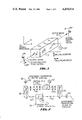
- FIG. 1 is an isometric sketch showing a conventional Pockels cell
- FIG. 2 is a sketch diagram of the physical organization of the system of this invention employing two Pockels cell modulators;
- FIG. 3 is a sketch diagram of an operating embodiment of the system of this invention.
- the system of this invention is a two-crystal electro-optic modulator using components of a conventional Pockels cell but configured so as to efficiently utilize the electro-optic effect of each of the two cells.
- the two crystal modulator Using LiTaO 3 crystals as the modulating medium for the Pockels effect, the two crystal modulator has been shown to have a full modulation switching voltage that is approximately one third of that required for a conventional Pockels cell configuration. As mentioned above, this greatly reduced power requirement has substantial advantages when compared to prior art modulation systems for almost all applications.
- FIG. 1 shows a conventional Pockels cell.
- the input laser beam 18 is polarized at an angle 14, here 45° to the C axis of the LiTaO 3 crystal.
- the crystal here has the three crystal axes 22 as shown in FIG. 1 with axis C being hereinafter referred to as the optical axis of the crystal.
- the crystal resolves this 45° input beam into an ordinary (O) component 26 with O being perpendicular to the C axis and an extraordinary (E) component 28 with E being parallel to the C axis of the crystal such that both the E and O components are of equal amplitude.
- O ordinary
- E extraordinary
- the O and E components Upon emerging from the crystal 10, the O and E components recombine to reproduce some output polarization state of the output beam 20, depending upon the net retardation, ⁇ , which is the difference in phase shift between the two components, E and O. If ⁇ is equal to some even number of half waves (n ⁇ /radians) the output polarization is linear and parallel to the input; but, if ⁇ is equal to an odd number of half waves, the sign of one component is reversed and the output polarization is linear and perpendicular to the input polarization direction. This case is illustrated in FIG. 1 with the output electrical field vector being oriented at -45° relative to the C axis of the crystal and the input electrical field vector of the beam being oriented at +45° to the C axis of the crystal.
- the transmission of a conventional modulator between crossed polarizers is:
- n e and n o are the extraordinary and ordinary refractive indices
- r 33 and r 13 are the electro-optic coefficients
- V is the applied voltage
- d is the crystal thickness
- the two-crystal modulator system of this invention achieves an approximately three-fold reduction in switching voltage by using two separate crystals in a configuration that uses the full electro-optic effect for the E polarization alone in both crystals.
- a diagram of the physical layout of this system is shown schematically in FIG. 2.
- the input beam 30 is resolved into two linearly polarized components of equal intensity 32 and 34 by a beam splitting polarization prism 36.
- the beams are focused into the two crystals by a means shown here as a single input lens 49 before the prism 36.
- These beams 32 and 34 then enter the two crystal modulators 38 and 40 where both beams propagate as pure E waves.
- the output beams 42 and 44 are then recombined by an ouput prism 46 which is substantially identical to the input prism 36.
- the output from the output prism is then recollimated by an output lens 50.
- the two crystals may be incorporated into traveling wave structures as a means to maximize wide band operation when connected as shown in the figure. However, such a construction is not necessary for low voltage operation.
- the modulation of the crystals is accomplished by impressing an effective voltage, V s , 52 across the crystal faces of each crystal which are perpendicular to the C optical axes of the respective crystals.
- the voltage is applied in opposite senses to the two crystals with respect to the positive C axis such that the phase shifts are in opposite directions. This can be accomplished by orienting the two crystals so the positive directions of the C axis are opposite.
- the phase shifts V v and V h induced in the vertically and horizontally polarized arms are given by: ##EQU4##
- the modulator crystals used in the experiment when treated as individual Pockels cells, should have full switching voltages of 57 volts when operated in a conventional manner.
- the full switching voltage for each crystal was 52 volts for crystal no. 1 and 56 volts for crystal no. 2.
- the ratio for equation (8) is equal to: ##EQU8##
- FIG. 3 An operational low voltage laser modulator system was then constructed along the lines shown in FIG. 3. This also was built as a traveling-wave structure to demonstrate the feasibility of ultra-high speed binary polarization modulation. This particular operating embodiment was modified slightly to facilitate fabrication and optical alignment when compared to the diagram shown in FIG. 2.
- the two modulator crystals 72 were bonded to a substrate and connected to a microstrip 70 to form the electrical transmission line.
- the input optical beam 60 was split into two equal intensity components by the polarization beam splitter 62.
- the half wave plate ( ⁇ /2 plate) 64 rotates the polarization of the light in the upper leg of the optical transmission path by 90° such that the laser light travels as pure E waves in both crystals.
- the optical time delay 66 provides proper timing of the optical signal and electrical wave form at the lower crystal.
- the timing at the upper crystal can be adjusted electrically.
- the light along each leg is then focused into the appropriate crystal by action of the respective lenses 68.
- the output beams from the crystals are then transmitted through the respective lenses 69.
- the beam then travels through another optical delay device 66 and then enters the polarization beam combiner 67.
- the output in the lower leg after transmission through the output lens 69 enters another half wave plate 64 and then into the polarization beam combiner 67 where it combines with the output beam from the upper leg to form the modulated output beam 72.
- the crystal ends have been anit-reflection coated.
- the use of a Brewster cut on the crystal faces is also possible and would entail only a mechanical redesign of the modulator.
- This particular prototype was electrically driven by a two-gigabit-per-second (Gbps) psuedo-noise (PN) source.
- the modulated optical signal was passed through another polarization beam splitter and detected using a high speed silicon avalanche photo diode.
- the results of the operation of this modulator demonstrated that effective ultra high speed optical modulation was obtainable through the use of this invention.
Landscapes
- Physics & Mathematics (AREA)
- Nonlinear Science (AREA)
- Chemical & Material Sciences (AREA)
- Engineering & Computer Science (AREA)
- Ceramic Engineering (AREA)
- Crystallography & Structural Chemistry (AREA)
- General Physics & Mathematics (AREA)
- Optics & Photonics (AREA)
- Optical Modulation, Optical Deflection, Nonlinear Optics, Optical Demodulation, Optical Logic Elements (AREA)
Abstract
Description
I.sub.t =I.sub.o Sin.sup.2 (Γ/2) (1)
Claims (9)
Priority Applications (1)
| Application Number | Priority Date | Filing Date | Title |
|---|---|---|---|
| US06/321,065 US4439014A (en) | 1981-11-13 | 1981-11-13 | Low voltage electro-optic modulator |
Applications Claiming Priority (1)
| Application Number | Priority Date | Filing Date | Title |
|---|---|---|---|
| US06/321,065 US4439014A (en) | 1981-11-13 | 1981-11-13 | Low voltage electro-optic modulator |
Publications (1)
| Publication Number | Publication Date |
|---|---|
| US4439014A true US4439014A (en) | 1984-03-27 |
Family
ID=23249036
Family Applications (1)
| Application Number | Title | Priority Date | Filing Date |
|---|---|---|---|
| US06/321,065 Expired - Fee Related US4439014A (en) | 1981-11-13 | 1981-11-13 | Low voltage electro-optic modulator |
Country Status (1)
| Country | Link |
|---|---|
| US (1) | US4439014A (en) |
Cited By (43)
| Publication number | Priority date | Publication date | Assignee | Title |
|---|---|---|---|---|
| US4850041A (en) * | 1987-05-13 | 1989-07-18 | Ford Aerospace & Communications Corporation | Laser radar with adjustable local oscillator |
| EP0422956A2 (en) * | 1989-10-13 | 1991-04-17 | Xerox Corporation | Multiple beam exposure control |
| EP0422957A2 (en) * | 1989-10-13 | 1991-04-17 | Xerox Corporation | Multiple beam optical modulation system |
| US5202789A (en) * | 1987-10-16 | 1993-04-13 | Kabushiki Kaisha Toshiba | Optical system for preserving a state of polarization of light beam |
| WO2000072079A2 (en) * | 1999-05-24 | 2000-11-30 | Marconi Applied Technologies Limited | Electro-optic devices |
| US20020167070A1 (en) * | 2000-06-30 | 2002-11-14 | Motorola, Inc. | Hybrid semiconductor structure and device |
| US6498358B1 (en) | 2001-07-20 | 2002-12-24 | Motorola, Inc. | Structure and method for fabricating an electro-optic system having an electrochromic diffraction grating |
| US20030022430A1 (en) * | 2001-07-24 | 2003-01-30 | Motorola, Inc. | Structure and method for fabricating configurable transistor devices utilizing the formation of a compliant substrate for materials used to form the same |
| US20030036217A1 (en) * | 2001-08-16 | 2003-02-20 | Motorola, Inc. | Microcavity semiconductor laser coupled to a waveguide |
| US6555946B1 (en) | 2000-07-24 | 2003-04-29 | Motorola, Inc. | Acoustic wave device and process for forming the same |
| US6589856B2 (en) | 2001-08-06 | 2003-07-08 | Motorola, Inc. | Method and apparatus for controlling anti-phase domains in semiconductor structures and devices |
| US6590236B1 (en) | 2000-07-24 | 2003-07-08 | Motorola, Inc. | Semiconductor structure for use with high-frequency signals |
| US6638838B1 (en) | 2000-10-02 | 2003-10-28 | Motorola, Inc. | Semiconductor structure including a partially annealed layer and method of forming the same |
| US6639249B2 (en) | 2001-08-06 | 2003-10-28 | Motorola, Inc. | Structure and method for fabrication for a solid-state lighting device |
| US20030207589A1 (en) * | 2002-05-03 | 2003-11-06 | Thoughtbeam, Inc. | Method for growing a monocrystalline oxide layer and for fabricating a semiconductor device on a monocrystalline substrate |
| US6646293B2 (en) | 2001-07-18 | 2003-11-11 | Motorola, Inc. | Structure for fabricating high electron mobility transistors utilizing the formation of complaint substrates |
| US6667196B2 (en) | 2001-07-25 | 2003-12-23 | Motorola, Inc. | Method for real-time monitoring and controlling perovskite oxide film growth and semiconductor structure formed using the method |
| US6673646B2 (en) | 2001-02-28 | 2004-01-06 | Motorola, Inc. | Growth of compound semiconductor structures on patterned oxide films and process for fabricating same |
| US6673667B2 (en) | 2001-08-15 | 2004-01-06 | Motorola, Inc. | Method for manufacturing a substantially integral monolithic apparatus including a plurality of semiconductor materials |
| US20040012037A1 (en) * | 2002-07-18 | 2004-01-22 | Motorola, Inc. | Hetero-integration of semiconductor materials on silicon |
| US6693298B2 (en) | 2001-07-20 | 2004-02-17 | Motorola, Inc. | Structure and method for fabricating epitaxial semiconductor on insulator (SOI) structures and devices utilizing the formation of a compliant substrate for materials used to form same |
| US6693033B2 (en) | 2000-02-10 | 2004-02-17 | Motorola, Inc. | Method of removing an amorphous oxide from a monocrystalline surface |
| US6709989B2 (en) | 2001-06-21 | 2004-03-23 | Motorola, Inc. | Method for fabricating a semiconductor structure including a metal oxide interface with silicon |
| US20040069991A1 (en) * | 2002-10-10 | 2004-04-15 | Motorola, Inc. | Perovskite cuprate electronic device structure and process |
| US20040070312A1 (en) * | 2002-10-10 | 2004-04-15 | Motorola, Inc. | Integrated circuit and process for fabricating the same |
| US20040150043A1 (en) * | 2003-02-03 | 2004-08-05 | Motorola, Inc. | Structure and method for fabricating semiconductor microresonator devices |
| US20040151463A1 (en) * | 2003-02-03 | 2004-08-05 | Motorola, Inc. | Optical waveguide structure and method for fabricating the same |
| US20040150076A1 (en) * | 2000-02-10 | 2004-08-05 | Motorola, Inc. | Semiconductor structure, semiconductor device, communicating device, integrated circuit, and process for fabricating the same |
| US20040164315A1 (en) * | 2003-02-25 | 2004-08-26 | Motorola, Inc. | Structure and device including a tunneling piezoelectric switch and method of forming same |
| US20040217444A1 (en) * | 2001-10-17 | 2004-11-04 | Motorola, Inc. | Method and apparatus utilizing monocrystalline insulator |
| US20040232431A1 (en) * | 2001-07-16 | 2004-11-25 | Motorola, Inc. | Semiconductor structure and method for implementing cross-point switch functionality |
| US20050023622A1 (en) * | 2000-05-31 | 2005-02-03 | Motorola | Semiconductor device and method |
| US20050056210A1 (en) * | 2000-07-24 | 2005-03-17 | Motorola | Heterojunction tunneling diodes and process for fabricating same |
| US6885065B2 (en) | 2002-11-20 | 2005-04-26 | Freescale Semiconductor, Inc. | Ferromagnetic semiconductor structure and method for forming the same |
| US20050135437A1 (en) * | 2003-12-18 | 2005-06-23 | Rice Robert R. | Bessel free electron laser device |
| US20050194593A1 (en) * | 2001-01-19 | 2005-09-08 | Freescale Semiconductor, Inc. | Structure and method for fabricating GaN devices utilizing the formation of a compliant substrate |
| US6992321B2 (en) | 2001-07-13 | 2006-01-31 | Motorola, Inc. | Structure and method for fabricating semiconductor structures and devices utilizing piezoelectric materials |
| US7019332B2 (en) | 2001-07-20 | 2006-03-28 | Freescale Semiconductor, Inc. | Fabrication of a wavelength locker within a semiconductor structure |
| US7045815B2 (en) | 2001-04-02 | 2006-05-16 | Freescale Semiconductor, Inc. | Semiconductor structure exhibiting reduced leakage current and method of fabricating same |
| US7161227B2 (en) | 2001-08-14 | 2007-01-09 | Motorola, Inc. | Structure and method for fabricating semiconductor structures and devices for detecting an object |
| US7169619B2 (en) | 2002-11-19 | 2007-01-30 | Freescale Semiconductor, Inc. | Method for fabricating semiconductor structures on vicinal substrates using a low temperature, low pressure, alkaline earth metal-rich process |
| US20100142046A1 (en) * | 2008-12-08 | 2010-06-10 | Gao Peiliang | Optical Isolator, Shutter, Variable Optical Attenuator and Modulator Device |
| WO2016008771A1 (en) * | 2014-07-14 | 2016-01-21 | University Of Copenhagen | Optical device having efficient light-matter interface for quantum simulations |
Citations (7)
| Publication number | Priority date | Publication date | Assignee | Title |
|---|---|---|---|---|
| US3429636A (en) * | 1964-02-07 | 1969-02-25 | Westinghouse Electric Corp | Electro-optical light modulation means using birefringent crystals |
| US3495892A (en) * | 1966-01-21 | 1970-02-17 | Rca Corp | Split beam light modulator |
| US3532890A (en) * | 1967-09-11 | 1970-10-06 | Bell Telephone Labor Inc | Optical multiplexing and demultiplexing systems |
| US3638024A (en) * | 1970-02-25 | 1972-01-25 | Bell Telephone Labor Inc | Optical pulse interval modulation system |
| US3684350A (en) * | 1970-08-17 | 1972-08-15 | Westinghouse Electric Corp | Light beam polarization modulator |
| US3956626A (en) * | 1973-06-14 | 1976-05-11 | Mcdonnell Douglas Corporation | Pulse quaternary communication means |
| US4145607A (en) * | 1976-12-16 | 1979-03-20 | Harry Bates | System and method for shaping pulses of optical radiation |
-
1981
- 1981-11-13 US US06/321,065 patent/US4439014A/en not_active Expired - Fee Related
Patent Citations (7)
| Publication number | Priority date | Publication date | Assignee | Title |
|---|---|---|---|---|
| US3429636A (en) * | 1964-02-07 | 1969-02-25 | Westinghouse Electric Corp | Electro-optical light modulation means using birefringent crystals |
| US3495892A (en) * | 1966-01-21 | 1970-02-17 | Rca Corp | Split beam light modulator |
| US3532890A (en) * | 1967-09-11 | 1970-10-06 | Bell Telephone Labor Inc | Optical multiplexing and demultiplexing systems |
| US3638024A (en) * | 1970-02-25 | 1972-01-25 | Bell Telephone Labor Inc | Optical pulse interval modulation system |
| US3684350A (en) * | 1970-08-17 | 1972-08-15 | Westinghouse Electric Corp | Light beam polarization modulator |
| US3956626A (en) * | 1973-06-14 | 1976-05-11 | Mcdonnell Douglas Corporation | Pulse quaternary communication means |
| US4145607A (en) * | 1976-12-16 | 1979-03-20 | Harry Bates | System and method for shaping pulses of optical radiation |
Cited By (63)
| Publication number | Priority date | Publication date | Assignee | Title |
|---|---|---|---|---|
| US4850041A (en) * | 1987-05-13 | 1989-07-18 | Ford Aerospace & Communications Corporation | Laser radar with adjustable local oscillator |
| US5202789A (en) * | 1987-10-16 | 1993-04-13 | Kabushiki Kaisha Toshiba | Optical system for preserving a state of polarization of light beam |
| EP0422956A2 (en) * | 1989-10-13 | 1991-04-17 | Xerox Corporation | Multiple beam exposure control |
| EP0422957A2 (en) * | 1989-10-13 | 1991-04-17 | Xerox Corporation | Multiple beam optical modulation system |
| EP0422957A3 (en) * | 1989-10-13 | 1992-05-20 | Xerox Corporation | Multiple beam optical modulation system |
| EP0422956A3 (en) * | 1989-10-13 | 1992-05-27 | Xerox Corporation | Multiple beam exposure control |
| WO2000072079A2 (en) * | 1999-05-24 | 2000-11-30 | Marconi Applied Technologies Limited | Electro-optic devices |
| WO2000072079A3 (en) * | 1999-05-24 | 2001-12-13 | Marconi Applied Techn Ltd | Electro-optic devices |
| GB2351356A (en) * | 1999-05-24 | 2000-12-27 | Marconi Applied Techn Ltd | Electro-optic devices |
| US6693033B2 (en) | 2000-02-10 | 2004-02-17 | Motorola, Inc. | Method of removing an amorphous oxide from a monocrystalline surface |
| US20040149202A1 (en) * | 2000-02-10 | 2004-08-05 | Motorola, Inc. | Semiconductor structure, semiconductor device, communicating device, integrated circuit, and process for fabricating the same |
| US20040232525A1 (en) * | 2000-02-10 | 2004-11-25 | Motorola, Inc. | Semiconductor structure, semiconductor device, communicating device, integrated circuit, and process for fabricating the same |
| US7067856B2 (en) | 2000-02-10 | 2006-06-27 | Freescale Semiconductor, Inc. | Semiconductor structure, semiconductor device, communicating device, integrated circuit, and process for fabricating the same |
| US20040150003A1 (en) * | 2000-02-10 | 2004-08-05 | Motorola, Inc. | Semiconductor structure, semiconductor device, communicating device, integrated circuit, and process for fabricating the same |
| US20040150076A1 (en) * | 2000-02-10 | 2004-08-05 | Motorola, Inc. | Semiconductor structure, semiconductor device, communicating device, integrated circuit, and process for fabricating the same |
| US20050023622A1 (en) * | 2000-05-31 | 2005-02-03 | Motorola | Semiconductor device and method |
| US7005717B2 (en) | 2000-05-31 | 2006-02-28 | Freescale Semiconductor, Inc. | Semiconductor device and method |
| US20020167070A1 (en) * | 2000-06-30 | 2002-11-14 | Motorola, Inc. | Hybrid semiconductor structure and device |
| US6590236B1 (en) | 2000-07-24 | 2003-07-08 | Motorola, Inc. | Semiconductor structure for use with high-frequency signals |
| US20050056210A1 (en) * | 2000-07-24 | 2005-03-17 | Motorola | Heterojunction tunneling diodes and process for fabricating same |
| US6555946B1 (en) | 2000-07-24 | 2003-04-29 | Motorola, Inc. | Acoustic wave device and process for forming the same |
| US7105866B2 (en) | 2000-07-24 | 2006-09-12 | Freescale Semiconductor, Inc. | Heterojunction tunneling diodes and process for fabricating same |
| US6638838B1 (en) | 2000-10-02 | 2003-10-28 | Motorola, Inc. | Semiconductor structure including a partially annealed layer and method of forming the same |
| US20050194593A1 (en) * | 2001-01-19 | 2005-09-08 | Freescale Semiconductor, Inc. | Structure and method for fabricating GaN devices utilizing the formation of a compliant substrate |
| US7211852B2 (en) | 2001-01-19 | 2007-05-01 | Freescale Semiconductor, Inc. | Structure and method for fabricating GaN devices utilizing the formation of a compliant substrate |
| US6673646B2 (en) | 2001-02-28 | 2004-01-06 | Motorola, Inc. | Growth of compound semiconductor structures on patterned oxide films and process for fabricating same |
| US7045815B2 (en) | 2001-04-02 | 2006-05-16 | Freescale Semiconductor, Inc. | Semiconductor structure exhibiting reduced leakage current and method of fabricating same |
| US6709989B2 (en) | 2001-06-21 | 2004-03-23 | Motorola, Inc. | Method for fabricating a semiconductor structure including a metal oxide interface with silicon |
| US6992321B2 (en) | 2001-07-13 | 2006-01-31 | Motorola, Inc. | Structure and method for fabricating semiconductor structures and devices utilizing piezoelectric materials |
| US20040232431A1 (en) * | 2001-07-16 | 2004-11-25 | Motorola, Inc. | Semiconductor structure and method for implementing cross-point switch functionality |
| US6646293B2 (en) | 2001-07-18 | 2003-11-11 | Motorola, Inc. | Structure for fabricating high electron mobility transistors utilizing the formation of complaint substrates |
| US6498358B1 (en) | 2001-07-20 | 2002-12-24 | Motorola, Inc. | Structure and method for fabricating an electro-optic system having an electrochromic diffraction grating |
| US7019332B2 (en) | 2001-07-20 | 2006-03-28 | Freescale Semiconductor, Inc. | Fabrication of a wavelength locker within a semiconductor structure |
| US6693298B2 (en) | 2001-07-20 | 2004-02-17 | Motorola, Inc. | Structure and method for fabricating epitaxial semiconductor on insulator (SOI) structures and devices utilizing the formation of a compliant substrate for materials used to form same |
| US6855992B2 (en) | 2001-07-24 | 2005-02-15 | Motorola Inc. | Structure and method for fabricating configurable transistor devices utilizing the formation of a compliant substrate for materials used to form the same |
| US20030022430A1 (en) * | 2001-07-24 | 2003-01-30 | Motorola, Inc. | Structure and method for fabricating configurable transistor devices utilizing the formation of a compliant substrate for materials used to form the same |
| US6667196B2 (en) | 2001-07-25 | 2003-12-23 | Motorola, Inc. | Method for real-time monitoring and controlling perovskite oxide film growth and semiconductor structure formed using the method |
| US6589856B2 (en) | 2001-08-06 | 2003-07-08 | Motorola, Inc. | Method and apparatus for controlling anti-phase domains in semiconductor structures and devices |
| US6639249B2 (en) | 2001-08-06 | 2003-10-28 | Motorola, Inc. | Structure and method for fabrication for a solid-state lighting device |
| US7161227B2 (en) | 2001-08-14 | 2007-01-09 | Motorola, Inc. | Structure and method for fabricating semiconductor structures and devices for detecting an object |
| US6673667B2 (en) | 2001-08-15 | 2004-01-06 | Motorola, Inc. | Method for manufacturing a substantially integral monolithic apparatus including a plurality of semiconductor materials |
| US20030036217A1 (en) * | 2001-08-16 | 2003-02-20 | Motorola, Inc. | Microcavity semiconductor laser coupled to a waveguide |
| US20040217444A1 (en) * | 2001-10-17 | 2004-11-04 | Motorola, Inc. | Method and apparatus utilizing monocrystalline insulator |
| US7342276B2 (en) | 2001-10-17 | 2008-03-11 | Freescale Semiconductor, Inc. | Method and apparatus utilizing monocrystalline insulator |
| US20030207589A1 (en) * | 2002-05-03 | 2003-11-06 | Thoughtbeam, Inc. | Method for growing a monocrystalline oxide layer and for fabricating a semiconductor device on a monocrystalline substrate |
| US6916717B2 (en) | 2002-05-03 | 2005-07-12 | Motorola, Inc. | Method for growing a monocrystalline oxide layer and for fabricating a semiconductor device on a monocrystalline substrate |
| US20040012037A1 (en) * | 2002-07-18 | 2004-01-22 | Motorola, Inc. | Hetero-integration of semiconductor materials on silicon |
| US20040070312A1 (en) * | 2002-10-10 | 2004-04-15 | Motorola, Inc. | Integrated circuit and process for fabricating the same |
| US20040069991A1 (en) * | 2002-10-10 | 2004-04-15 | Motorola, Inc. | Perovskite cuprate electronic device structure and process |
| US7169619B2 (en) | 2002-11-19 | 2007-01-30 | Freescale Semiconductor, Inc. | Method for fabricating semiconductor structures on vicinal substrates using a low temperature, low pressure, alkaline earth metal-rich process |
| US6885065B2 (en) | 2002-11-20 | 2005-04-26 | Freescale Semiconductor, Inc. | Ferromagnetic semiconductor structure and method for forming the same |
| US20040151463A1 (en) * | 2003-02-03 | 2004-08-05 | Motorola, Inc. | Optical waveguide structure and method for fabricating the same |
| US7020374B2 (en) | 2003-02-03 | 2006-03-28 | Freescale Semiconductor, Inc. | Optical waveguide structure and method for fabricating the same |
| US6965128B2 (en) | 2003-02-03 | 2005-11-15 | Freescale Semiconductor, Inc. | Structure and method for fabricating semiconductor microresonator devices |
| US20040150043A1 (en) * | 2003-02-03 | 2004-08-05 | Motorola, Inc. | Structure and method for fabricating semiconductor microresonator devices |
| US20040164315A1 (en) * | 2003-02-25 | 2004-08-26 | Motorola, Inc. | Structure and device including a tunneling piezoelectric switch and method of forming same |
| US7046703B2 (en) | 2003-12-18 | 2006-05-16 | The Boeing Company | Bessel free electron laser device |
| US20050135437A1 (en) * | 2003-12-18 | 2005-06-23 | Rice Robert R. | Bessel free electron laser device |
| US20100142046A1 (en) * | 2008-12-08 | 2010-06-10 | Gao Peiliang | Optical Isolator, Shutter, Variable Optical Attenuator and Modulator Device |
| US8351117B2 (en) | 2008-12-08 | 2013-01-08 | Gao Peiliang | Optical isolator, shutter, variable optical attenuator and modulator device |
| WO2016008771A1 (en) * | 2014-07-14 | 2016-01-21 | University Of Copenhagen | Optical device having efficient light-matter interface for quantum simulations |
| US20170160474A1 (en) * | 2014-07-14 | 2017-06-08 | University Of Copenhagen | Optical device having efficient light-matter interface for quantum simulations |
| US9798083B2 (en) * | 2014-07-14 | 2017-10-24 | University Of Copenhagen | Optical device having efficient light-matter interface for quantum simulations |
Similar Documents
| Publication | Publication Date | Title |
|---|---|---|
| US4439014A (en) | Low voltage electro-optic modulator | |
| US3684350A (en) | Light beam polarization modulator | |
| US5020050A (en) | Cascadable optical combinatorial logic gates | |
| US4474435A (en) | Polarization-insensitive optical switch and multiplexing apparatus | |
| US3407364A (en) | Intracavity laser phase modulator | |
| US3532890A (en) | Optical multiplexing and demultiplexing systems | |
| US5005952A (en) | Polarization controller | |
| EP0081177A2 (en) | Polarization-insensitive optical switch and multiplexing apparatus | |
| JP2022526208A (en) | Orbital angular momentum generators and methods for polarization-modulated orbital angular momentum | |
| Rumbaugh et al. | Polarization control for coherent fiber-optic systems using nematic liquid crystals | |
| US4514046A (en) | Polarization-insensitive optical switch and multiplexing apparatus | |
| JPH02275411A (en) | High speed modulator for changing polarization state of optical carrier | |
| GB2271192A (en) | Optical switch | |
| US3600587A (en) | Frequency shift keying laser communication system | |
| JP3777045B2 (en) | Polarization scrambler | |
| JPH07152005A (en) | Optical device | |
| US6958845B2 (en) | Optical control element | |
| US3356438A (en) | Light modulator employing multiplereflective light path | |
| US3900247A (en) | Optical modulator having compensation for thermal and space charge effects | |
| US3366792A (en) | Laser intracavity phase modulator | |
| JP3249884B2 (en) | Apparatus and method for modulating polarized light signal | |
| GB1100506A (en) | High speed laser frequency selector | |
| US3392353A (en) | Maser intracavity phase modulator | |
| US4145607A (en) | System and method for shaping pulses of optical radiation | |
| US3957340A (en) | Electrooptical amplitude modulator |
Legal Events
| Date | Code | Title | Description |
|---|---|---|---|
| AS | Assignment |
Owner name: MCDONNELL DOUGLAS CORPORATION, A CORP. OF MD Free format text: ASSIGNMENT OF ASSIGNORS INTEREST.;ASSIGNORS:STACY, ROBERT A.;RICE, ROBERT R.;REEL/FRAME:003954/0986 Effective date: 19811103 Owner name: MCDONNELL DOUGLAS CORPORATION, A CORP. OF MD, MARY Free format text: ASSIGNMENT OF ASSIGNORS INTEREST;ASSIGNORS:STACY, ROBERT A.;RICE, ROBERT R.;REEL/FRAME:003954/0986 Effective date: 19811103 |
|
| MAFP | Maintenance fee payment |
Free format text: PAYMENT OF MAINTENANCE FEE, 4TH YEAR, PL 96-517 (ORIGINAL EVENT CODE: M170); ENTITY STATUS OF PATENT OWNER: LARGE ENTITY Year of fee payment: 4 |
|
| FEPP | Fee payment procedure |
Free format text: MAINTENANCE FEE REMINDER MAILED (ORIGINAL EVENT CODE: REM.); ENTITY STATUS OF PATENT OWNER: LARGE ENTITY |
|
| LAPS | Lapse for failure to pay maintenance fees | ||
| FP | Lapsed due to failure to pay maintenance fee |
Effective date: 19920329 |
|
| STCH | Information on status: patent discontinuation |
Free format text: PATENT EXPIRED DUE TO NONPAYMENT OF MAINTENANCE FEES UNDER 37 CFR 1.362 |