US3582673A - Interference-free multivibrator switching circuit using saturated undoped transistors with large base-to-emitter capacity - Google Patents
Interference-free multivibrator switching circuit using saturated undoped transistors with large base-to-emitter capacity Download PDFInfo
- Publication number
- US3582673A US3582673A US771722A US3582673DA US3582673A US 3582673 A US3582673 A US 3582673A US 771722 A US771722 A US 771722A US 3582673D A US3582673D A US 3582673DA US 3582673 A US3582673 A US 3582673A
- Authority
- US
- United States
- Prior art keywords
- base
- transistor
- transistors
- emitter
- current
- Prior art date
- Legal status (The legal status is an assumption and is not a legal conclusion. Google has not performed a legal analysis and makes no representation as to the accuracy of the status listed.)
- Expired - Lifetime
Links
Images
Classifications
-
- H—ELECTRICITY
- H03—ELECTRONIC CIRCUITRY
- H03K—PULSE TECHNIQUE
- H03K3/00—Circuits for generating electric pulses; Monostable, bistable or multistable circuits
- H03K3/02—Generators characterised by the type of circuit or by the means used for producing pulses
- H03K3/26—Generators characterised by the type of circuit or by the means used for producing pulses by the use, as active elements, of bipolar transistors with internal or external positive feedback
- H03K3/28—Generators characterised by the type of circuit or by the means used for producing pulses by the use, as active elements, of bipolar transistors with internal or external positive feedback using means other than a transformer for feedback
- H03K3/281—Generators characterised by the type of circuit or by the means used for producing pulses by the use, as active elements, of bipolar transistors with internal or external positive feedback using means other than a transformer for feedback using at least two transistors so coupled that the input of one is derived from the output of another, e.g. multivibrator
- H03K3/286—Generators characterised by the type of circuit or by the means used for producing pulses by the use, as active elements, of bipolar transistors with internal or external positive feedback using means other than a transformer for feedback using at least two transistors so coupled that the input of one is derived from the output of another, e.g. multivibrator bistable
-
- H—ELECTRICITY
- H03—ELECTRONIC CIRCUITRY
- H03K—PULSE TECHNIQUE
- H03K3/00—Circuits for generating electric pulses; Monostable, bistable or multistable circuits
- H03K3/02—Generators characterised by the type of circuit or by the means used for producing pulses
- H03K3/26—Generators characterised by the type of circuit or by the means used for producing pulses by the use, as active elements, of bipolar transistors with internal or external positive feedback
- H03K3/28—Generators characterised by the type of circuit or by the means used for producing pulses by the use, as active elements, of bipolar transistors with internal or external positive feedback using means other than a transformer for feedback
- H03K3/281—Generators characterised by the type of circuit or by the means used for producing pulses by the use, as active elements, of bipolar transistors with internal or external positive feedback using means other than a transformer for feedback using at least two transistors so coupled that the input of one is derived from the output of another, e.g. multivibrator
Definitions
- ABSTRACT In a multivibrator-type switching circuit using transistors which are switched from a cutoff to a saturation condition, the base circuit of each transistor is arranged to supply to the base of the transistor, when the latter is in a saturated condition, a current which is at least five times, typically between five and 10 times, the maximum collector current of the transistor divided by the minimum common emitter current gain.
- this base current which is far above that normally employed in this type of circuit, the charge on the base-to-emitter capacity is increased thereby requiring considerably higher energy to cause malfunction.
- the circuit is thus much less susceptible to misoperation due to interferring signals than prior types of circuits.
- Multivibrator-type switching circuits are commonlyused, inter alia, in logic circuits for control apparatus.
- transistors are usually employed in the construction of bistable and other multivibrator-type switching circuits.
- one of the problems met with in such control apparatus is the inadvertent switching of the multivibrator-type logic circuits due to such interference. It is one of the objects of the present invention to provide an improved form of multivibrator-type circuits reducing the risk of inadvertent switching due to interference.
- the base circuit of each transistor is arranged to supply to the base of the transistor, when the latter isin a saturated condition, a current which is at least five times the maximum collector current of the transistor divided by the minimum common emitter current gain.
- the base current in each transistor, when this transistor is in a saturated condition would be made between five and times the maximum collector current divided by the minimum common emitter current gain.
- the object of increasing the base current far above that nor mally employed in this type of circuit is to increase the charge on the base to emitter capacity of the transistor.
- Thetransistor is preferably chosen to be of a type having a large base to emitter capacity when in saturation and which is not doped to cause the charge in this capacity to leak away internally. With this arrangement the major part of the saturated base to emitter charge for each transistor has to flow out of the base lead of the transistor. Thus, with-the increased charge due to the higher base current, a considerably higher energy in the millicoulomb range is required to causemalfunction'of the circuit.
- the circuit is thereby very much less susceptible to mis' operation clue to interferring signals than prior circuits which have been designed in the orthodox way to have a maximum base current equal to the maximum collector current divided by the minimum common emitter current gain and using conventional transistors which are doped to cause internal dissipation of any charge in the emitter-tobase capacity.
- Transistors for switching circuits are normally designed nowadays so that, on removing the base saturation signal, the base to emitter charge is dispersed internally in the transistor with only a small amount of charge flowing out of the base lead. This is done to decrease the saturation time constant T (which is defined as the ratio of the saturation base charge to the saturation base current). To improve the highfrequency performance of transistors, this saturation time constant has to be kept to a minimum. For many control purposes however, high frequency performance is not important and, for the purposes of the present invention, it is preferable that the charge on the base-to-emitter capacity should have to flow out through the base lead of the transistor and not be dissipated internally in the transistor.
- the transistor used should, under forced bias saturation conditions, have a T, in the region of l microsecond or more. The higher the T value, and more immune to interference the circuit becomes. Therefore I microsecond is a compromise between immunity from interference and speed of switching.
- the circuit of the present invention is conveniently formed as an integrated circuit, the whole of the circuit being formed on a single semiconductor chip or substrate.
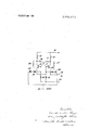
- the circuit shown in the drawing employs two transistors 10, 11 which are of the type described above having high base to emitter capacity when in saturation and which are not doped to cause internal leakage of the base to emitter charge.
- the collectors of the transistors 10, 11 are connected respectively by resistors l2, 13 to a first supply line 14 and the emitters are connected to earth at 15.
- the collector of the transistor 10 is connected to the base of the transistor 11 by a resistor 16 and the collector of transistor 11 is connected to the base of the transistor 10 by a resistor 17.
- the bases of the transistors 10, 11 are connected by resistors l8, l9 respectively to a supply line 20.
- Input signals at an input 21 are applied to the bases of the two transistors through capacitors 22, 23 and rectifiers 24, 25.
- the collector of the transistor 10 is connected to the junction between the capacitor 22 and rectifier 24 by a resistor 26 and the collector of transistor 11 is connected to the junction between the capacitor 23 and rectifier 25 by a resistor 27.
- the potentiometer networks feeding the bases of the transistors 10, 11 are formed by the resistors 13, I7 and 18, and 12, 16 and 19 respectively and these networks are arranged so that the base current fed into each transistor, when it is in the on condition, is between five and 10 times the maximum collector current divided by the minimum common emitter current gain.
- the total resistance of each of these potentiometer networks is therefore considerably lower than is used in conventional practice where the maximum base current is commonly made equal to the maximum collector current divided by the minimum common emitter current gain.
- the circuit may be formed as an in tegrated circuit on a single germanium or silicon chip or substrate.
- a multivibrator-type switching circuit using two transistors with interconnecting circuit means operative to switch the transistors alternately from a cutoff to a saturation condition
- the improvement comprising the provisions of a base circuit for eachtransistor arranged to supply to the base of each transistor in a saturated condition a base current at least five times the maximum collector current of the transistor when saturated divided by the minimum physically realizable common emitter current gain of the transistor, said transistors being of a type having a large base-to-emitter capacitance during saturation conditions and an absence of doping in the base-to-emitter region whereby the major part of the saturated base-to-emitter charge for each transistor flows out of the base lead of the transistor.
- a multivibrator-type switching circuit comprising first and second transistors, each having an emitter, a collector and a base, said transistors are undoped in the base-to-emitter region, a direct voltage supply having first and second terminals, two collector loads in series respectively with the collectors of the transistors between the collectors and said first terminal, first and second resistors connecting respectively the collectors of the first-transistor to the base of the second transistor and the collector of the'second transistor to the base of the first transistor, third and fourth resistors connecting the bases time constant of at least 1 microsecond and having a large base to emitter Capacity when in saturation, and the loads and first, second, third and fourth resistors being arranged so that the base current fed into each transistor, when it is in the saturated condition, is between five and 10 times the maximum collector current divided by the minimum common emitter current gain.
Landscapes
- Engineering & Computer Science (AREA)
- Power Engineering (AREA)
- Electronic Switches (AREA)
- Bipolar Integrated Circuits (AREA)
Abstract
In a multivibrator-type switching circuit using transistors which are switched from a cutoff to a saturation condition, the base circuit of each transistor is arranged to supply to the base of the transistor, when the latter is in a saturated condition, a current which is at least five times, typically between five and 10 times, the maximum collector current of the transistor divided by the minimum common emitter current gain. By using this base current, which is far above that normally employed in this type of circuit, the charge on the base-to-emitter capacity is increased thereby requiring considerably higher energy to cause malfunction. The circuit is thus much less susceptible to misoperation due to interferring signals than prior types of circuits.
Description
United States Patent Appl. No. Filed Patented Assignee INTERFERENCE-F REE MULTIVIBRATOR SWITCHING CIRCUIT USING SATURATED UNDOPED TRANSISTORS WITH LARGE BASE-T0- EMITTER CAPACITY 3 Claims, 1 Drawing Fig.
US. Cl; 307/202, 307/272, 307/280, 307/292, 307/300 Int. Cl H02h 7/20 Field of Search 307/272, 273, 276, 280, 289, 290, 291 292, 300, 202
References Cited UNITED STATES PATENTS 3/1961' Lohmon 3/1966 Madsen etal 10/1967 Leenhoutz OTHER REFERENCES Hurley, R. B., Transistor Electronics, John Wiley &'
Sons, N. Y. (pgs. 363- 367) (1958).
ABSTRACT: In a multivibrator-type switching circuit using transistors which are switched from a cutoff to a saturation condition, the base circuit of each transistor is arranged to supply to the base of the transistor, when the latter is in a saturated condition, a current which is at least five times, typically between five and 10 times, the maximum collector current of the transistor divided by the minimum common emitter current gain. By using this base current, which is far above that normally employed in this type of circuit, the charge on the base-to-emitter capacity is increased thereby requiring considerably higher energy to cause malfunction. The circuit is thus much less susceptible to misoperation due to interferring signals than prior types of circuits.
PATENTEUJUN H91: 3582- 673 AQWMQ M: 7 a mw/% Mm INTERFERENCE-FREE MULTIVIBRATOR SWITCHING CIRCUIT USING SATURATED UNDOPEI) TRANSISTORS WITH LARGE BASE-TO-EMI'ITER CAPACITY BACKGROUND OF THE INVENTION 1. Field of the Invention This invention relates to multivibratortype switching circuits. The expression multivibrator-type circuits is to be understood to include bistable, monostable and astable circuits.
2. Description of the Prior Art Multivibrator-type switching circuits are commonlyused, inter alia, in logic circuits for control apparatus. Nowadays transistors are usually employed in the construction of bistable and other multivibrator-type switching circuits. Particularly with apparatus for the control of machine tools and the like, there are liable to be strong electrical interferring fields and one of the problems met with in such control apparatus is the inadvertent switching of the multivibrator-type logic circuits due to such interference. It is one of the objects of the present invention to provide an improved form of multivibrator-type circuits reducing the risk of inadvertent switching due to interference.
SUMMARY OF THE INVENTION According to this invention, in a multivibrator-type switching circuit using transistors which are switched from a cutoff to a saturation condition, the base circuit of each transistor is arranged to supply to the base of the transistor, when the latter isin a saturated condition, a current which is at least five times the maximum collector current of the transistor divided by the minimum common emitter current gain. Typically the base current in each transistor, when this transistor is in a saturated condition, would be made between five and times the maximum collector current divided by the minimum common emitter current gain.
The object of increasing the base current far above that nor mally employed in this type of circuit is to increase the charge on the base to emitter capacity of the transistor. Thetransistor is preferably chosen to be of a type having a large base to emitter capacity when in saturation and which is not doped to cause the charge in this capacity to leak away internally. With this arrangement the major part of the saturated base to emitter charge for each transistor has to flow out of the base lead of the transistor. Thus, with-the increased charge due to the higher base current, a considerably higher energy in the millicoulomb range is required to causemalfunction'of the circuit. The circuit is thereby very much less susceptible to mis' operation clue to interferring signals than prior circuits which have been designed in the orthodox way to have a maximum base current equal to the maximum collector current divided by the minimum common emitter current gain and using conventional transistors which are doped to cause internal dissipation of any charge in the emitter-tobase capacity.
Transistors for switching circuits are normally designed nowadays so that, on removing the base saturation signal, the base to emitter charge is dispersed internally in the transistor with only a small amount of charge flowing out of the base lead. This is done to decrease the saturation time constant T (which is defined as the ratio of the saturation base charge to the saturation base current). To improve the highfrequency performance of transistors, this saturation time constant has to be kept to a minimum. For many control purposes however, high frequency performance is not important and, for the purposes of the present invention, it is preferable that the charge on the base-to-emitter capacity should have to flow out through the base lead of the transistor and not be dissipated internally in the transistor. Thus, as previously mentioned, for the purposes of the present invention, one preferably uses a transistor with a large base to emitter capacity and which is not doped to cause this charge to leak away internally. In practice, the transistor used should, under forced bias saturation conditions, have a T, in the region of l microsecond or more. The higher the T value, and more immune to interference the circuit becomes. Therefore I microsecond is a compromise between immunity from interference and speed of switching.
The circuit of the present invention is conveniently formed as an integrated circuit, the whole of the circuit being formed on a single semiconductor chip or substrate.
BRIEF DESCRIPTION OF THE DRAWING The accompanying drawing is a circuit diagram of a bistable circuit forming one embodiment of the invention.
DESCRIPTION OF THE PREFERRED EMBODIMENT The circuit shown in the drawing employs two transistors 10, 11 which are of the type described above having high base to emitter capacity when in saturation and which are not doped to cause internal leakage of the base to emitter charge. The collectors of the transistors 10, 11 are connected respectively by resistors l2, 13 to a first supply line 14 and the emitters are connected to earth at 15. The collector of the transistor 10 is connected to the base of the transistor 11 by a resistor 16 and the collector of transistor 11 is connected to the base of the transistor 10 by a resistor 17. The bases of the transistors 10, 11 are connected by resistors l8, l9 respectively to a supply line 20. Input signals at an input 21 are applied to the bases of the two transistors through capacitors 22, 23 and rectifiers 24, 25. The collector of the transistor 10 is connected to the junction between the capacitor 22 and rectifier 24 by a resistor 26 and the collector of transistor 11 is connected to the junction between the capacitor 23 and rectifier 25 by a resistor 27.
The potentiometer networks feeding the bases of the transistors 10, 11 are formed by the resistors 13, I7 and 18, and 12, 16 and 19 respectively and these networks are arranged so that the base current fed into each transistor, when it is in the on condition, is between five and 10 times the maximum collector current divided by the minimum common emitter current gain. For this purpose the total resistance of each of these potentiometer networks is therefore considerably lower than is used in conventional practice where the maximum base current is commonly made equal to the maximum collector current divided by the minimum common emitter current gain.
As previously indicated the circuit may be formed as an in tegrated circuit on a single germanium or silicon chip or substrate.
We claim:
1. In a multivibrator-type switching circuit using two transistors with interconnecting circuit means operative to switch the transistors alternately from a cutoff to a saturation condition, the improvement comprising the provisions of a base circuit for eachtransistor arranged to supply to the base of each transistor in a saturated condition a base current at least five times the maximum collector current of the transistor when saturated divided by the minimum physically realizable common emitter current gain of the transistor, said transistors being of a type having a large base-to-emitter capacitance during saturation conditions and an absence of doping in the base-to-emitter region whereby the major part of the saturated base-to-emitter charge for each transistor flows out of the base lead of the transistor.
2. A multivibrator-type switching circuit as claimed in claim I wherein the transistors have a saturation time constant of at least 1 microsecond.
3. A multivibrator-type switching circuit comprising first and second transistors, each having an emitter, a collector and a base, said transistors are undoped in the base-to-emitter region, a direct voltage supply having first and second terminals, two collector loads in series respectively with the collectors of the transistors between the collectors and said first terminal, first and second resistors connecting respectively the collectors of the first-transistor to the base of the second transistor and the collector of the'second transistor to the base of the first transistor, third and fourth resistors connecting the bases time constant of at least 1 microsecond and having a large base to emitter Capacity when in saturation, and the loads and first, second, third and fourth resistors being arranged so that the base current fed into each transistor, when it is in the saturated condition, is between five and 10 times the maximum collector current divided by the minimum common emitter current gain.
Claims (3)
1. In a multivibrator-type switching circuit using two transistors with interconnecting circuit means operative to switch the transistors alternately from a cutoff to a saturation condition, the improvement comprising the provisions of a base circuit for each transistor arranged to supply to the base of each transistor in a saturated condition a base current at least five times the maximum collector current of the transistor when saturated divided by the minimum physically realizable common emitter current gain of the transistor, said transistors being of a type having a large base-to-emitter capacitance during saturation conditions and an absence of doping in the base-toemitter region whereby the major part of the saturated base-toemitter charge for each transistor flows out of the base lead of the transistor.
2. A multivibrator-type switching circuit as claimed in claim 1 wherein the transistors have a saturation time constant of at least 1 microsecond.
3. A multivibrator-type switching circuit comprising first and second transistors, each having an emitter, a collector and a base, said transistors are undoped in the base-to-emitter region, a direct voltage supply having first and second terminals, two collector loads in series respectively with the collectors of the transistors between the collectors and said first terminal, first and second resistors connecting respectively the collectors of the first transistor to the base of the second transistor and the collector of the second transistor to the base of the first transistor, third and fourth resistors connecting the bases of the first and second transistors respectively to said second terminal, a connection between the emitters of the two transistors and ground, a fifth resistor in series with a first rectifier between the collector and the base of the first transistor, a sixth resistor in series with a second rectifier between the collector and base of the second transistor, and an input circuit capacitively connected to the junction of the fifth resistor and first rectifier and the junction of the sixth resistor and second rectifier, said transistors having a saturation time constant of at least 1 microsecond and having a large base to emitter capacity when in saturation, and the loads and first, second, third and fourth resistors being arranged so that the base current fed into each transistor, when it is in the saturated condition, is between five and 10 times the maximum collector current divided by the minimum common emitter current gain.
Applications Claiming Priority (3)
| Application Number | Priority Date | Filing Date | Title |
|---|---|---|---|
| GB27400/67A GB1169110A (en) | 1967-06-14 | 1967-06-14 | Improvements in or relating to Multivibrator Type Switching Circuits |
| DE1802583A DE1802583C3 (en) | 1967-06-14 | 1968-10-11 | Multivibrator circuit |
| US77172268A | 1968-10-30 | 1968-10-30 |
Publications (1)
| Publication Number | Publication Date |
|---|---|
| US3582673A true US3582673A (en) | 1971-06-01 |
Family
ID=27181533
Family Applications (1)
| Application Number | Title | Priority Date | Filing Date |
|---|---|---|---|
| US771722A Expired - Lifetime US3582673A (en) | 1967-06-14 | 1968-10-30 | Interference-free multivibrator switching circuit using saturated undoped transistors with large base-to-emitter capacity |
Country Status (3)
| Country | Link |
|---|---|
| US (1) | US3582673A (en) |
| DE (1) | DE1802583C3 (en) |
| GB (1) | GB1169110A (en) |
Cited By (2)
| Publication number | Priority date | Publication date | Assignee | Title |
|---|---|---|---|---|
| WO1990016068A1 (en) * | 1989-06-15 | 1990-12-27 | Bipolar Integrated Technology, Inc. | Soft error immune memory |
| US5463345A (en) * | 1993-01-07 | 1995-10-31 | Nec Corporation | Circuit for converting unipolar input to bipolar output |
Citations (3)
| Publication number | Priority date | Publication date | Assignee | Title |
|---|---|---|---|---|
| US2974238A (en) * | 1957-11-04 | 1961-03-07 | Rca Corp | Multivibrator circuit |
| US3241017A (en) * | 1963-06-27 | 1966-03-15 | Superior Electric Co | Pulse supplying device employing variable-oscillator and presettable counter for controlling speed and direction of motor |
| US3345521A (en) * | 1966-02-17 | 1967-10-03 | Superior Electric Co | Decimal coded binary counter with sequential digit input |
-
1967
- 1967-06-14 GB GB27400/67A patent/GB1169110A/en not_active Expired
-
1968
- 1968-10-11 DE DE1802583A patent/DE1802583C3/en not_active Expired
- 1968-10-30 US US771722A patent/US3582673A/en not_active Expired - Lifetime
Patent Citations (3)
| Publication number | Priority date | Publication date | Assignee | Title |
|---|---|---|---|---|
| US2974238A (en) * | 1957-11-04 | 1961-03-07 | Rca Corp | Multivibrator circuit |
| US3241017A (en) * | 1963-06-27 | 1966-03-15 | Superior Electric Co | Pulse supplying device employing variable-oscillator and presettable counter for controlling speed and direction of motor |
| US3345521A (en) * | 1966-02-17 | 1967-10-03 | Superior Electric Co | Decimal coded binary counter with sequential digit input |
Non-Patent Citations (1)
| Title |
|---|
| Hurley, R. B., Transistor Electronics, John Wiley & Sons, N. Y. (pgs. 363 367) (1958). * |
Cited By (3)
| Publication number | Priority date | Publication date | Assignee | Title |
|---|---|---|---|---|
| WO1990016068A1 (en) * | 1989-06-15 | 1990-12-27 | Bipolar Integrated Technology, Inc. | Soft error immune memory |
| US5043939A (en) * | 1989-06-15 | 1991-08-27 | Bipolar Integrated Technology, Inc. | Soft error immune memory |
| US5463345A (en) * | 1993-01-07 | 1995-10-31 | Nec Corporation | Circuit for converting unipolar input to bipolar output |
Also Published As
| Publication number | Publication date |
|---|---|
| DE1802583C3 (en) | 1974-09-12 |
| DE1802583B2 (en) | 1971-04-15 |
| DE1802583A1 (en) | 1970-04-23 |
| GB1169110A (en) | 1969-10-29 |
Similar Documents
| Publication | Publication Date | Title |
|---|---|---|
| US3416043A (en) | Integrated anti-ringing clamped logic circuits | |
| US3535532A (en) | Integrated circuit including light source,photodiode and associated components | |
| US2676271A (en) | Transistor gate | |
| EP0032046A2 (en) | Circuitry for protecting a semiconductor device against static electricity | |
| US3394268A (en) | Logic switching circuit | |
| GB753014A (en) | Semiconductor electric signal translating devices | |
| US3241043A (en) | Thyratron tube replacement unit employing a zener diode limiting the inverse voltageacross a gating transistor | |
| US3217181A (en) | Logic switching circuit comprising a plurality of discrete inputs | |
| US3735151A (en) | Output circuit for comparators | |
| US3716722A (en) | Temperature compensation for logic circuits | |
| GB766210A (en) | Electrical circuit employing a semiconductor | |
| US3505535A (en) | Digital circuit with antisaturation collector load network | |
| US3790817A (en) | Schottky clamped ttl circuit | |
| US3562547A (en) | Protection diode for integrated circuit | |
| US2895058A (en) | Semiconductor devices and systems | |
| US2939967A (en) | Bistable semiconductor circuit | |
| US2901639A (en) | Semi-conductor multivibrator circuit | |
| US3473047A (en) | High speed digital logic circuit having non-saturating output transistor | |
| US3487233A (en) | Detector with upper and lower threshold points | |
| US2888578A (en) | Transistor emitter-follower circuits | |
| US3582673A (en) | Interference-free multivibrator switching circuit using saturated undoped transistors with large base-to-emitter capacity | |
| US3194977A (en) | Temperature-stabilized transistor multivibrator | |
| US3649846A (en) | Single supply comparison amplifier | |
| US3544808A (en) | High speed saturation mode switching circuit for a capacitive load | |
| US3253165A (en) | Current steering logic circuit employing negative resistance devices in the output networks of the amplifying devices |