US2980809A - Semi-conductor devices for rectifying and clipping large electrical currents - Google Patents
Semi-conductor devices for rectifying and clipping large electrical currents Download PDFInfo
- Publication number
- US2980809A US2980809A US701478A US70147857A US2980809A US 2980809 A US2980809 A US 2980809A US 701478 A US701478 A US 701478A US 70147857 A US70147857 A US 70147857A US 2980809 A US2980809 A US 2980809A
- Authority
- US
- United States
- Prior art keywords
- current
- voltage
- transistor
- elements
- electrode
- Prior art date
- Legal status (The legal status is an assumption and is not a legal conclusion. Google has not performed a legal analysis and makes no representation as to the accuracy of the status listed.)
- Expired - Lifetime
Links
- 239000004065 semiconductor Substances 0.000 title description 16
- 239000003990 capacitor Substances 0.000 description 58
- 208000019300 CLIPPERS Diseases 0.000 description 37
- 208000021930 chronic lymphocytic inflammation with pontine perivascular enhancement responsive to steroids Diseases 0.000 description 37
- 230000005669 field effect Effects 0.000 description 21
- 238000000034 method Methods 0.000 description 20
- 238000011144 upstream manufacturing Methods 0.000 description 16
- 230000008569 process Effects 0.000 description 14
- 238000010586 diagram Methods 0.000 description 13
- 238000009826 distribution Methods 0.000 description 12
- 230000002441 reversible effect Effects 0.000 description 10
- 230000000903 blocking effect Effects 0.000 description 7
- 230000007423 decrease Effects 0.000 description 7
- 230000000694 effects Effects 0.000 description 7
- 230000005284 excitation Effects 0.000 description 7
- 238000004804 winding Methods 0.000 description 7
- 230000005540 biological transmission Effects 0.000 description 6
- 229910052732 germanium Inorganic materials 0.000 description 6
- GNPVGFCGXDBREM-UHFFFAOYSA-N germanium atom Chemical compound [Ge] GNPVGFCGXDBREM-UHFFFAOYSA-N 0.000 description 6
- XUIMIQQOPSSXEZ-UHFFFAOYSA-N Silicon Chemical compound [Si] XUIMIQQOPSSXEZ-UHFFFAOYSA-N 0.000 description 5
- 229910052710 silicon Inorganic materials 0.000 description 5
- 239000010703 silicon Substances 0.000 description 5
- 230000036961 partial effect Effects 0.000 description 4
- 239000004020 conductor Substances 0.000 description 3
- 238000007599 discharging Methods 0.000 description 3
- 239000000463 material Substances 0.000 description 3
- 230000009471 action Effects 0.000 description 2
- 230000004888 barrier function Effects 0.000 description 2
- 230000000295 complement effect Effects 0.000 description 2
- 238000009792 diffusion process Methods 0.000 description 2
- 238000010304 firing Methods 0.000 description 2
- 230000004048 modification Effects 0.000 description 2
- 238000012986 modification Methods 0.000 description 2
- 230000009467 reduction Effects 0.000 description 2
- 230000003068 static effect Effects 0.000 description 2
- OAICVXFJPJFONN-UHFFFAOYSA-N Phosphorus Chemical compound [P] OAICVXFJPJFONN-UHFFFAOYSA-N 0.000 description 1
- VYPSYNLAJGMNEJ-UHFFFAOYSA-N Silicium dioxide Chemical compound O=[Si]=O VYPSYNLAJGMNEJ-UHFFFAOYSA-N 0.000 description 1
- 101150004141 Vcan gene Proteins 0.000 description 1
- 230000002159 abnormal effect Effects 0.000 description 1
- 230000003321 amplification Effects 0.000 description 1
- 238000013459 approach Methods 0.000 description 1
- 229910052785 arsenic Inorganic materials 0.000 description 1
- RQNWIZPPADIBDY-UHFFFAOYSA-N arsenic atom Chemical compound [As] RQNWIZPPADIBDY-UHFFFAOYSA-N 0.000 description 1
- 230000033228 biological regulation Effects 0.000 description 1
- 239000002800 charge carrier Substances 0.000 description 1
- 229910052729 chemical element Inorganic materials 0.000 description 1
- 238000010276 construction Methods 0.000 description 1
- 230000001419 dependent effect Effects 0.000 description 1
- 238000013461 design Methods 0.000 description 1
- 238000011161 development Methods 0.000 description 1
- 230000005684 electric field Effects 0.000 description 1
- 230000002349 favourable effect Effects 0.000 description 1
- 238000010438 heat treatment Methods 0.000 description 1
- 239000012535 impurity Substances 0.000 description 1
- 230000000977 initiatory effect Effects 0.000 description 1
- 238000009434 installation Methods 0.000 description 1
- 238000009413 insulation Methods 0.000 description 1
- 238000012423 maintenance Methods 0.000 description 1
- QSHDDOUJBYECFT-UHFFFAOYSA-N mercury Chemical compound [Hg] QSHDDOUJBYECFT-UHFFFAOYSA-N 0.000 description 1
- 229910052753 mercury Inorganic materials 0.000 description 1
- 238000003199 nucleic acid amplification method Methods 0.000 description 1
- 229910052698 phosphorus Inorganic materials 0.000 description 1
- 239000011574 phosphorus Substances 0.000 description 1
- 230000000135 prohibitive effect Effects 0.000 description 1
- LFULEKSKNZEWOE-UHFFFAOYSA-N propanil Chemical compound CCC(=O)NC1=CC=C(Cl)C(Cl)=C1 LFULEKSKNZEWOE-UHFFFAOYSA-N 0.000 description 1
- QHGVXILFMXYDRS-UHFFFAOYSA-N pyraclofos Chemical compound C1=C(OP(=O)(OCC)SCCC)C=NN1C1=CC=C(Cl)C=C1 QHGVXILFMXYDRS-UHFFFAOYSA-N 0.000 description 1
- 230000000717 retained effect Effects 0.000 description 1
- 230000035939 shock Effects 0.000 description 1
- 239000000126 substance Substances 0.000 description 1
- 230000001960 triggered effect Effects 0.000 description 1
- 238000009827 uniform distribution Methods 0.000 description 1
Images


Classifications
-
- H—ELECTRICITY
- H03—ELECTRONIC CIRCUITRY
- H03G—CONTROL OF AMPLIFICATION
- H03G11/00—Limiting amplitude; Limiting rate of change of amplitude ; Clipping in general
- H03G11/002—Limiting amplitude; Limiting rate of change of amplitude ; Clipping in general without controlling loop
-
- C—CHEMISTRY; METALLURGY
- C03—GLASS; MINERAL OR SLAG WOOL
- C03C—CHEMICAL COMPOSITION OF GLASSES, GLAZES OR VITREOUS ENAMELS; SURFACE TREATMENT OF GLASS; SURFACE TREATMENT OF FIBRES OR FILAMENTS MADE FROM GLASS, MINERALS OR SLAGS; JOINING GLASS TO GLASS OR OTHER MATERIALS
- C03C25/00—Surface treatment of fibres or filaments made from glass, minerals or slags
- C03C25/10—Coating
- C03C25/24—Coatings containing organic materials
- C03C25/40—Organo-silicon compounds
-
- C—CHEMISTRY; METALLURGY
- C07—ORGANIC CHEMISTRY
- C07F—ACYCLIC, CARBOCYCLIC OR HETEROCYCLIC COMPOUNDS CONTAINING ELEMENTS OTHER THAN CARBON, HYDROGEN, HALOGEN, OXYGEN, NITROGEN, SULFUR, SELENIUM OR TELLURIUM
- C07F7/00—Compounds containing elements of Groups 4 or 14 of the Periodic Table
- C07F7/02—Silicon compounds
- C07F7/08—Compounds having one or more C—Si linkages
- C07F7/0834—Compounds having one or more O-Si linkage
-
- C—CHEMISTRY; METALLURGY
- C08—ORGANIC MACROMOLECULAR COMPOUNDS; THEIR PREPARATION OR CHEMICAL WORKING-UP; COMPOSITIONS BASED THEREON
- C08G—MACROMOLECULAR COMPOUNDS OBTAINED OTHERWISE THAN BY REACTIONS ONLY INVOLVING UNSATURATED CARBON-TO-CARBON BONDS
- C08G77/00—Macromolecular compounds obtained by reactions forming a linkage containing silicon with or without sulfur, nitrogen, oxygen or carbon in the main chain of the macromolecule
- C08G77/04—Polysiloxanes
- C08G77/38—Polysiloxanes modified by chemical after-treatment
- C08G77/382—Polysiloxanes modified by chemical after-treatment containing atoms other than carbon, hydrogen, oxygen or silicon
- C08G77/388—Polysiloxanes modified by chemical after-treatment containing atoms other than carbon, hydrogen, oxygen or silicon containing nitrogen
-
- G—PHYSICS
- G05—CONTROLLING; REGULATING
- G05F—SYSTEMS FOR REGULATING ELECTRIC OR MAGNETIC VARIABLES
- G05F1/00—Automatic systems in which deviations of an electric quantity from one or more predetermined values are detected at the output of the system and fed back to a device within the system to restore the detected quantity to its predetermined value or values, i.e. retroactive systems
- G05F1/10—Regulating voltage or current
- G05F1/12—Regulating voltage or current wherein the variable actually regulated by the final control device is AC
- G05F1/40—Regulating voltage or current wherein the variable actually regulated by the final control device is AC using discharge tubes or semiconductor devices as final control devices
- G05F1/44—Regulating voltage or current wherein the variable actually regulated by the final control device is AC using discharge tubes or semiconductor devices as final control devices semiconductor devices only
-
- H—ELECTRICITY
- H02—GENERATION; CONVERSION OR DISTRIBUTION OF ELECTRIC POWER
- H02H—EMERGENCY PROTECTIVE CIRCUIT ARRANGEMENTS
- H02H7/00—Emergency protective circuit arrangements specially adapted for specific types of electric machines or apparatus or for sectionalised protection of cable or line systems, and effecting automatic switching in the event of an undesired change from normal working conditions
- H02H7/10—Emergency protective circuit arrangements specially adapted for specific types of electric machines or apparatus or for sectionalised protection of cable or line systems, and effecting automatic switching in the event of an undesired change from normal working conditions for converters; for rectifiers
- H02H7/12—Emergency protective circuit arrangements specially adapted for specific types of electric machines or apparatus or for sectionalised protection of cable or line systems, and effecting automatic switching in the event of an undesired change from normal working conditions for converters; for rectifiers for static converters or rectifiers
- H02H7/125—Emergency protective circuit arrangements specially adapted for specific types of electric machines or apparatus or for sectionalised protection of cable or line systems, and effecting automatic switching in the event of an undesired change from normal working conditions for converters; for rectifiers for static converters or rectifiers for rectifiers
- H02H7/127—Emergency protective circuit arrangements specially adapted for specific types of electric machines or apparatus or for sectionalised protection of cable or line systems, and effecting automatic switching in the event of an undesired change from normal working conditions for converters; for rectifiers for static converters or rectifiers for rectifiers having auxiliary control electrode to which blocking control voltages or currents are applied in case of emergency
-
- H—ELECTRICITY
- H02—GENERATION; CONVERSION OR DISTRIBUTION OF ELECTRIC POWER
- H02H—EMERGENCY PROTECTIVE CIRCUIT ARRANGEMENTS
- H02H9/00—Emergency protective circuit arrangements for limiting excess current or voltage without disconnection
- H02H9/02—Emergency protective circuit arrangements for limiting excess current or voltage without disconnection responsive to excess current
- H02H9/025—Current limitation using field effect transistors
-
- H—ELECTRICITY
- H02—GENERATION; CONVERSION OR DISTRIBUTION OF ELECTRIC POWER
- H02M—APPARATUS FOR CONVERSION BETWEEN AC AND AC, BETWEEN AC AND DC, OR BETWEEN DC AND DC, AND FOR USE WITH MAINS OR SIMILAR POWER SUPPLY SYSTEMS; CONVERSION OF DC OR AC INPUT POWER INTO SURGE OUTPUT POWER; CONTROL OR REGULATION THEREOF
- H02M7/00—Conversion of AC power input into DC power output; Conversion of DC power input into AC power output
- H02M7/02—Conversion of AC power input into DC power output without possibility of reversal
- H02M7/04—Conversion of AC power input into DC power output without possibility of reversal by static converters
- H02M7/12—Conversion of AC power input into DC power output without possibility of reversal by static converters using discharge tubes with control electrode or semiconductor devices with control electrode
- H02M7/145—Conversion of AC power input into DC power output without possibility of reversal by static converters using discharge tubes with control electrode or semiconductor devices with control electrode using devices of a thyratron or thyristor type requiring extinguishing means
- H02M7/155—Conversion of AC power input into DC power output without possibility of reversal by static converters using discharge tubes with control electrode or semiconductor devices with control electrode using devices of a thyratron or thyristor type requiring extinguishing means using semiconductor devices only
- H02M7/19—Conversion of AC power input into DC power output without possibility of reversal by static converters using discharge tubes with control electrode or semiconductor devices with control electrode using devices of a thyratron or thyristor type requiring extinguishing means using semiconductor devices only arranged for operation in series, e.g. for voltage multiplication
-
- H—ELECTRICITY
- H02—GENERATION; CONVERSION OR DISTRIBUTION OF ELECTRIC POWER
- H02M—APPARATUS FOR CONVERSION BETWEEN AC AND AC, BETWEEN AC AND DC, OR BETWEEN DC AND DC, AND FOR USE WITH MAINS OR SIMILAR POWER SUPPLY SYSTEMS; CONVERSION OF DC OR AC INPUT POWER INTO SURGE OUTPUT POWER; CONTROL OR REGULATION THEREOF
- H02M7/00—Conversion of AC power input into DC power output; Conversion of DC power input into AC power output
- H02M7/02—Conversion of AC power input into DC power output without possibility of reversal
- H02M7/04—Conversion of AC power input into DC power output without possibility of reversal by static converters
- H02M7/12—Conversion of AC power input into DC power output without possibility of reversal by static converters using discharge tubes with control electrode or semiconductor devices with control electrode
- H02M7/21—Conversion of AC power input into DC power output without possibility of reversal by static converters using discharge tubes with control electrode or semiconductor devices with control electrode using devices of a triode or transistor type requiring continuous application of a control signal
- H02M7/217—Conversion of AC power input into DC power output without possibility of reversal by static converters using discharge tubes with control electrode or semiconductor devices with control electrode using devices of a triode or transistor type requiring continuous application of a control signal using semiconductor devices only
- H02M7/25—Conversion of AC power input into DC power output without possibility of reversal by static converters using discharge tubes with control electrode or semiconductor devices with control electrode using devices of a triode or transistor type requiring continuous application of a control signal using semiconductor devices only arranged for operation in series, e.g. for multiplication of voltage
-
- H—ELECTRICITY
- H10—SEMICONDUCTOR DEVICES; ELECTRIC SOLID-STATE DEVICES NOT OTHERWISE PROVIDED FOR
- H10D—INORGANIC ELECTRIC SEMICONDUCTOR DEVICES
- H10D99/00—Subject matter not provided for in other groups of this subclass
Definitions
- TEszNER 2,980,809 SEMI-CONDUCTOR DEVICES F OR RECTIF'YING AND CLIPPING LARGE ELECTRICAL CURRENTS Filed Deo. 9, 1957 10 Sheets-Sheet 5 April 18, 1961 Filed Dec. 9, 1957 S TESZNER SEMI-CONDUCTOR D'EVICES FOR RECTIF'YING AND CLIPPING LARGE ELECTRICAL CURRENTS l0 Sheets-Sheet 4 ⁇ /o l 21 11 H i ⁇ 5 11 1 -zvo ⁇ /a vo Camp;
- SEMI-CONDUCTOR DEVICES FCE RECTIFYINC AND CLIPPINC LARGE ELECTRICAL CURRENTS g-mulslms TESINE/E Inh/HTW [fr: 6.3, 5AFF/7L Afin/HE] April 18, 1961 s.
- the present 'invention relates' t'oseini-conduc'tor devices for rectifying' and clippingl lage electrical currents.
- the loss in power within the rectifier may be indeed very slight but it is by no means negligible.
- the evacuation of the resulting heat entails the use of radiators 'necessitating a considerable increase of rectifier bulk.
- the heating effect is particularly troublesome for germanium junction rectifiersfwhic'h have a maximum operating temperature in the order of 80 G5, and .to a lesser 2 extent for silicon rectifiers which will accept temperatures in the order of to 200 C., although, here also, relatively bulky radiators are essential.
- Self-limitation of the current and a measure of regulation of the distribution of the voltage in the elements in series could be achieved by means of a device utilizing two series junctions of opposite type of conductivity, generally referred to as n-p-n or p-n-p transistors: by suitably biasing the intermediate portion called the, base it is possible to adjust the ramplitude of the current flowing at a given voltage to render it practically unidirectional orto limit its amplitude.
- this device suiiers from the major drawback of possessing excessive resistance that causes a prohibitive drop in potential. ⁇ The same obtains when the device is utilized for current clipping applications.
- the purpose of the present invention is to produce a device capable of functioning either as a rectifier or as an automatic current clipper, offering, as a rectifier, a forward resistance and, as a current clipper, a forward and reverse resistance that can practically be as low as. desired and, yet assure a self current-clipping function and permit easy control of thevoltage distribution in the respective elements.
- a device does not offer the various above mentioned drawbacks that are Va feature ofboth rectifiers and junction transistors. It can be produced for all working voltages, provided the elements are connected in series, and for all workingcurrents, provided the elements are connected in parallel.
- the invention utilizes a device referred to as a unipolar eld-effect transistor.
- Transistors of that type are described notably in my copending patent application Ser. No. 701,670, filed December 9, 1957, now Patent No. 2,930,950.
- a unipolar transistor described in my above mentioned application takes the form of a plurality of cylindrical rods of monocrystal semi-conductive substance, suchl as germanium or silicon, for example, integral with a common base and fitted at vboth ends with an electrode in acsasa ohmc contact with the semi-conductor and with an ntermediate electrode encircling the rod and separated from the semi-conductor body by a space charge consisting, for example, of a barrier surface, and, possibly, by an additional insulating film.
- the intermediate electrode is referred to as the gate electrode and the terminal electrodes as drain and source electrodes respectively, it being understood that, in bi-directional ow conditions of operation, in the caseV of alternating current operation, the respective functions of the two terminal electrodes are inverted .over each half-wave of current.
- the invention consists, when the field-effect transistor operates in an-alternating current rectifier function, in assuring the cutting-off of the current over every other half lWave by biasing the gate. with respect to the source electrode by means of a series of quasi-rectangular wave voltage pulses, the duration of the individual pulses and the gap between the pulses being equal to the duration of a half-wave and the amplitudes of the pulses being at least equal to that of the total pinch-off voltage.
- the bias voltages of these elements can be adjusted so that their respective resistances over the blocked half-wave period be practically the same for all elements, thereby assuring a uniform distribution of the reverse voltage in the elements.
- the invention also consists in assuring the cutting-off of the forward current in the event of partial or total short-circuiting of the load, such cut-off being obtained by means of a complemenary biasing of the gate, it being also understood that the presence of the gate electrode can be utilized to assure all other control functions, as would a control grid in a mercury vapour rectifier (but without the overloading hazards inherent to this latter device).
- the invention consists, on the other hand, when the unipolar transistor is operated in an alternating current clipping function, incharging the gate electrode of at least one transistor with a voltage pulse in phase with the current, which pulse is produced immediately the predetermined current limit is reached.
- the invention also relates to the constitution of a chain of elements having on both sides at least one bounding element the biasing of which is assured by the above-defined voltage pulse; depending upon the particular current half-wave during which the predetermined limit is reached, the biasing pulse will be applied to the up-stream or the down-stream bounding element, the elements being interconnected in a manner such that the cutting-off of at least one terminal element causes the cutting-off in cascade of the other elements.
- the in vention also relates to a system of automatic releasewithin a predetermined time delay assuring the resumption of the operation, with current clipping operation possible immediately afterwards, should faulty conditions subsist, this sequence of operation being repeatable at will.
- the invention also relates to a direct current clipper which is derived from 'the preceding device.
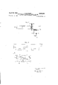
- Fig. l represents the circuit diagram of an earliertype of cylindrical shape unipolar transistor of the prior art.
- Fig. 2 shows the family of characteristic curves for such a transistor.
- Fig. 3 and Fig. 4 represent a unipolar power transistor of the prior art described in myv above-mentioned copending application.
- Fig. 5 and Fig. 6 represent in schematic form a power rectifier conforming to the invention,'and a graph explaining its functioning.
- Fig. 7 and Fig. 8 represent a complementary rectifier control circuit assuring the cutting-ofi' of the forward current in the event'of a short-circuit, and the graph exp-lain ing the functioning of the rectifier embodying such a device.
- Fig. 9 is a diagram of principle of the automatic energizing of an alternating current clipper comprising two series elements.
- Fig. l0 represents in schematic form a current clipper embodying several elements in cascade, comprising two chains of series elements.
- Fig. 1l and Fig. 12 represent a graph explaining the functioning of, and a circuitdiagram describing a current clipper embodying only one chain of series elements.
- Fig. 13 and Fig. 14v represent characteristic curves of the functioning of a current clipper.
- Fig. 15 is the circuit diagram of an elementary clipper.
- Fig. 16 and Fig. 17 represent a basic current clipper embodying an automatic release system operating within a predetermined time delay and a diagram of interconnection with the basic limiters adjacentv to the chain.
- Fig. 18 represents a current clipper embodying a system of automatic release.
- Fig. 19 represents a direct current clipper and Fig. 20 and Fig. 2l represent unipolar transistors of the prior art suitable for the constitution of rectifiers and clippers according to theinvention.
- Fig. l which shows the ⁇ circuit diagram of a unipolar field-effect transistor ofthe prior art
- '81' represents the semi-conductor rod of thetransistor
- 82 and 83 the terminal electrodes forming respectively the source and the drain
- 84 the electrode enabling the setting-up of a transverse field within th'esemi-conductor, which field assures the modulation of the portion of the channel which carries the current generated by source 85.
- Electrodes 82 and 83 are welded to the terminals of body 81 so as to assure ohmic contact, wh'er'easelectrode 84 is insulated with respect to that body by means of a barrier surface with, possibly, an intermediate insulating film or, alternatively, by a so-called n-p junction.
- f On electrode 84 act, on the one hand bias source 86, and on the other the signal produced by generatorl 87, which signal is applied, after amplification. to external load 88.
- Fig. 2 shows the family of characteristic drain voltage drain current curves for different gate bias voltages, Ia, Va and Vg being the drain current and voltage and the gate bias voltage respectively. These curves were recorded on the cylindrical shape transistors, therefore of the centripetal pinch-off effecttype, according to my above mentioned patent.
- unipolar power transistors comprising a plurality of cylindrical shape rods, such as described in the above mentioned patent application of December 9, 1957.
- a unipolar power transistor of that type a plan view of an element of such a transistor being represented in Fig. 3 and a partial diametrical sectional view of that element being represented to a larger scale in Fig. 4, embodies a thin plate 1 of given semiconductive material of predetermined resistivity.
- the surface of the plate will have an area of, for'example, 5 to 10 sq. cms.Y and its thickness will be 0.25 to 0.30 mm.
- the surface of the plate is plane and carefully polished.
- the plate is provided onone side with cylindrical rods or teeth 2, perpendicular to its surface, the manner in which such rods are obtained being described in the above mentioned application.
- the rods are laid out in regular pattern, for example, in concentric circles if plate 1 is circular or in staggered pattern if plate l is square or rectangular, or again, in a combination of the two patterns presenting maximum rod density, as illustrated in Fig. 3.
- Individual rod tips terminate into an ohmic contact 3 and a second ohmic contact 4 is located ov'er the plane surface of the plate, across the axis of each rod.
- Such ohmic contacts constitute the source and the drain of the individual unipolar transistors, the functions of said drain and source being -alternately reversible depending upon whether transistor is utilized in an alternating current rectifying or clipping function.
- the gate electrode 5 can be deposited about the rods without the need for an intermediate insulating film.
- Fig. 4 of my patent application of December 9, 1957 should be particularly referred to.
- Fig. 5 shows a theoretical diagram ⁇ of the circuit of;a rectifier consisting of two sets of transistors 21 and 22,
- Signal 23 is obtained for example as represented on Fig. 5 according to a'known practice consisting in starting from a source of alternating current 26 which is syn- ⁇ chronous with the principal source, supplying, through a large core-less inductance 27, a saturable core transformer 28. There is one such transformer per element. To obtain pulses that are of practically rectangular-shape, a relatively-high value of transformer ratio will have to be selected. The adjustment of the voltage distribution in the elements over the blocked'half-wave period can be easily obtained by permanently magnetizing the core of transformer 28 by means of an auxiliary winding 29, energized by an adjustable source of direct current 30.
- Fig. 7 shows the theoretical circuit diagram of a device assuring the cutting-off of the forward current of the rectifierA in the event of an overload considered as excessive, caused, ⁇ for example, by total or partial shortcircuiting of the load.
- the principle of the device consists in injecting into the control circuit of gate 5, during the period of forward half-wave, a signal of the same rectangular shape but of opposite sign and having three times the amplitude of the normal control voltage.
- Fig. 8, line a shows the shape 31 of the resulting control signal curve, as well as the corresponding values of minimum gate bias, respectively with respect to the drain (Fig. 8b) and to the source (Fig.
- the complementary cut-off voltage can be supplied, as represented for instance in Fig. 7, by a saturated-core transformer 32 having its secondary winding in series with that of transformer 28, such transformer being energized by a source of alternating current 34, through a rectifier 33.
- the system for closing the primary winding represented in schematic form by a three-electrode tube 35, can be provided by any device in general use, practically free of inertia, such as a thyratron or a transistor, the operation of which will be controlled by a signal set up by the excessive overload, according to one of lthe known systems already utilized for the grid control of mercury-vapour rectifiers.
- this impulse negatively charges Vat a potential larger than V0, a circuit comprising a capacitor 36 and a resistance 37 in parallel, connected between gate 5 and upstream terminal 11 in the case of upstream element 21 and between gate 5 and downstream terminal 12 in the case of downstream element 22.
- a charge is obtained in the following manner: v Y
- the two elements 21 and 22' are placed between current transformers 38 and 39, which transformers are theoretically of identical design.
- the voltage across the terminals of the circuit formed by resistance 44 and capacitor 40 in parallel, connected to the terminals of the secondary winding of each transformer becomes markedly larger than Vo and is large enough to initiate the tiring of a unidirectional valve, for example a thyratron 42.
- a unidirectional valve for example a thyratron 42.
- either valve 42 controlled by transformer 38 or the rvalve controlled by transformer 39 will fire.
- gate 5 is duly charged negatively with respect to the corresponding source, to a potential larger than V and current cut-off conditions are obtained, either by element 21 or by element 22'.
- the time constant for the process can be made very short. In actual practice, it is dependent only upon the residual resistance of valve 42 and of rectifier 43 which may be very low.
- the capacitance of the charging capacitor will obviously have to be markedly larger (for example to 10 times) than the capacitance of the capacitor 36 to be charged.
- the device embodied in the figure comprises two chains of elements 21 and 22', the right-hand and left-hand chains being connected in series.
- the circuit formed bycapacitor 3 6 and resistance 37 is connected to the upstream terminal 11 of the element, whereas in the second chainthe corresponding circuit is connected to the downstream terminal 12.
- Cascade excitation is obtained through use of voltage set up across the terminals of the element cut-off in the 'rst instance to bias the gate of the following element,
- the first drawback which is a minor one, is that the current tends to be restored over the half-wave following that over which the initial excitation was applied and this is the time when the second chain intervenes to cut-off the current completely, since an individual chain can cut-oi the current for only one half-wave.
- the second drawback which is a major one, is that the device necessitates two chains in series, the voltage drops Vacross these adding-up during normal operation. Consequently, for
- each element will require twice the number of transistors in parallel, this resulting in four times the quantity of material than would normally l: needed if'the device embodied'a single chain.
- Fig. 12 represents the circuit diagram of this principle, under the form of an alternating current clipper embodying a single chain of elements.
- This chain then comprises only those circuit Velements that are upstream with respect to capacitor 36. It is bounded by current transformers 48 and 49 which supply a voltage double that supplied by transformers 38 and 39.
- the upstream transformer 48 energizes the two initial elements 211 and 212, through resistance 44, capacitor 40, unidirectional valve 42. resistance 41 and high-frequency transformer 45, having two secondary windings charging the capacitors 36 of these elements through rectiers 43.
- the downstream transformer 49 charges only capacitor 36 of the final elementllx, (where n is the number of elements in the chain), but at double the voltage.
- the capacitor when the impulse originates Afrom the upstream direction, the capacitor is connected between the gate and the terminal functioning as the source electrode for the particular half-wave of current, whereas, when the impulse originates from the downstream direction, the capacitor'is connected between the gate and the drain electrode.
- the system for producing the initial impulse :from the current transformers is mentioned here only by way of example: such an impulse can also be generated by one of the known selective protection devices used in electrical network practice, exciting either one or the other Yend of the chain of elements.
- a purely electronic device should be preferred so as not to lose the advantages of instantaneous current clipper operation.
- Figs. 13 and 14 should be referred to. They give as'indications only, the curves representing, for an element, the drain current I,l as a function of the drain voltage Va for different gate bias voltages Vg (curves 46 in Fig. 13) and voltage Va as a function of Vg (curve 47 in Fig. 14).
- the nominal'working ⁇ current ,In (peak value) of the current clipper will causeonly a negligible voltage drop not detectable in the ligure, actually in the order of someten thousandths of the nominal working voltage Vn.
- thvalue of overload current controlling the operation Ofthecurrent clipper which value is assumed to'be Vin the ,order fof fZlm, this voltage drop will still be only'approximately'double the value of the preceding drop and .still undetectable -on the figure.
- Fig. 15 shows the detail of an element thus equipped and also shows the detail of the circuit embodying capacitor 36 and resistance 37.
- the shunting circuit of element 21 can consist of a xed linear resistance 52 assuring distribution up to the working voltage value, having, in parallel, a non-linear resistance 53, that is a resistance varying as an inverse function of the voltage across its terminals, correcting any possible discrepancy in the distribution at higher voltages.
- resistance 52 can be in the order of 50 ohms and resistance 53 can be of the order of 300 ohms at the working voltage, and vary in inverse proportion to the power 3 or 4 of the voltage. In this manner, the residual current at the Working voltage will be only in the order of 15 amperes R.M.S.
- Capacitor 36 can be shunted by a similar circuit: a fixed resistance 5t), setting the time-constant of the discharge, and a non-linear resistance 51, preventing any excessive rise of voltage across the capacitor.
- a fixed resistance 5t setting the time-constant of the discharge
- a non-linear resistance 51 preventing any excessive rise of voltage across the capacitor.
- the duration of the process actually amounts to that required for the charging of the corresponding capacitors 36.
- the charging time for the first two or for the last elements excited by the impulse originating from the current transformers is very short, as explained earlier; in actual fact, the charging time can be less than 1 microsecond.
- the charging of the following elements will be accomplished as the voltage is restored across the terminals; the charging time will therefore be a function of the natural frequency of the circuit in which the current clipper is functioning.
- current clipping can be effective after a time period of approximately 200 its., which means, assuming that the clipper operates for 2in, that current peak clipping oc,- curs within 41 or, at the most, within 10% of the shortcircuit current.
- the clipper be capable of restoring the system to normal working conditions within a predetermined period of time. This time delay is necessary for the fault, if that fault is of purely momentary nature, to suppress itself, arcing having quenched out and the arcing path being suiciently de-ionized to permit the voltage to be restored.
- the circuitbreaker 'automatically operates afterwards, for example 0.15 ns., the currentclipper being now ready to revert to normal working conditions, that is, to let the vcurrent through or 'tooperate again if lthe vfault persists.
- capacitor 363 of element 212 is shunted only 'by a non-linear resistance 54, the sole purpose of which is to limit the voltage across its terminals.
- it features a small rectifier 55 in series which rectifier prevents the capacitor from discharging Vthrough resistance 56.
- Rectifier' 55 is shunted by a transistor 57 which is biased negatively by the voltage ⁇ across the terminals of capacitor 362 of the adjacent element to the left.
- the bias voltage notably exceeds V0, as long as the bias voltage remains at least equal to that value, the transistor practically behaves like an infinite resistance, but as soon asit falls below that value, the resistance of the transistor decreases sharply,
- Capaclitor 363 is suppliedV through rectifiers 43 over one halfwave at the potential across the terminals of elements '12 v211 and 212 and over the other half-wave at the potential across the terminals'of elements 212 and 21.1.
- a foryWard current' is always owing through rectifier 5S.
- capacitors 361 and 362 discharge through their respective shunting resistances 62, which resistances will preferablyY consist, as mentioned earlier, of a unipolar 4transistor having its gate electrode connected to the source,
- elements 211 and 212 are sufficiently unblocked for the potential across their terminals to become practically negligible; simultaneously, transistor 57 shunting the rectifier 55 ⁇ loses its bias. Capacitor 363 then discharges suddenly through this transistor, the natural resistances of elements 211 and 212 and through resistance 56.
- the value of this last resistance is'selected so that it is high with respect to the forward resistance of rectifier 43 and markedly higher than shunting resistances 52,'53 of the elements, Vso as not to perturb the charge across capacitor 363 during cut-off conditions, but sufficiently low to reduce to a minimum the discharging time-constant of that capacitor.
- the value of that resistance 56 can be 200 ohms, thereby giving, with a capacitance of 0.1 nf., for capacitor 363, a time-constant in the order of 20 lts. However, half-way through this time period, the Voltage across the terminals of capacitor 363 will have dropped sufficiently to unblock the element 212 and also to remove the bias from transistor 57 of element 214.
- the upstream transformer 48 is replaced by transformer 58, the secondary winding of which features a center tap: with this arrangement, whatever the current half-wave, one of the capacitors 40 or 40"will be always Vcharged negatively.”
- this .valve operates and generates an impulse which charges, through the high frequency transformer 45. the capaci- .tors 361 and' 362 of the first two elements 211, and 212.
- the alternating current clipper embodying the above fcircuit is capable of clipping the short'circuit current at avalue. which is practically harmless and to assure vioursly be produced on the same principles.
- lthe problem is evenY more simple, due to the fact that 4the respective positions of the drain and source are permanent. For that reason, ⁇ the circuit diagram can be considerably streamlined.
- Fig. 19 gives the principle.
- the current clipper represented in Athe diagram ⁇ is suitable' for application in a ⁇ direct-current network of 1500 to 2000 volts;
- the interval between the gate and the source vof the ⁇ individual elements is shunted by a capacitor, respectively 601, 602, 603.
- a capacitor respectively 601, 602, 603.
- a resistance -62 consisting of a ⁇ unipolar transisto-r having Kits gate connected to the source, and for the following elements, another unipolar transistor 632,633 having its gate controlled by the voltage from capacitor 60 of the adjacent upstream element.
- the initial impulse can be -generated by a transformer 68 having its secondary winding shunted by an impedance 64,"preferably comprising a capacitance of a value larger than that of capacitor 60.
- an impedance 64 preferably comprising a capacitance of a value larger than that of capacitor 60.
- a unidirectional electric valve (thyratron 65) is connected across this impedance, in series with a resistance 66 across which is placed the capacitor 60 of therst 'element 611 through the'rectifierV 67.
- the normal overload sets up across the impedance 61V a voltage of suitable sign andhaving an amplitude suiicient to iire valve 65.
- a voltage impulse sets up across resistance 66 Y charging capacitor 601 through rectifier 67, of the' first upstream element 611.
- This capacitor can charge Yup very rapidly owing to the capacitance value ofthe ca- Apacitor included in the circuit of impedance 64.
- the charging voltage exceeds the voltage value of complete pinch-off Vo.
- Restoring of normal working conditions within aLpredetermined delay can, here also, be achieved through 'the use oa circuit breaker in series. In this case, ca-
- pacitors601, 602, 602 would be shunted iby simple fixed vresistances "On the other hand, it is, in this particular case, very easyzto obtain completely automatic restoring of .the working conditions; shunting ⁇ by transistors 62632L+632 represented in Fig. 19 corresponds to this latter possibility.
- the system operates 'zas "follows:
- yCapacitor 601 of'thegfirst upstream element 611 dis- charges according lto 'the time-constant of the circuit #601-"62; the rate fofidischarge is relatively slow at rst ⁇ -and accelerates'fvvith ⁇ the decrease in voltage across 601.
- 4transistor 632 of the second element is unblocked and initiatesa sudden discharge of the corresponding 'capacitor '602, Vreleases elementr ⁇ 612 and, Apractically simultaneously, releases the third elementfan'd other elements if required, accordingy to an identical process.
- the current clipper is obviously ready to operate again should the cause of its first operation ysubsist.
- Va A rectifier capable of supplying 4000 amperesat 1500 to 2000 volts direct current
- Figs, 2O and 21 recall the structure of known unipolar transistors which can possibly be utilized for the embodment of the elements'of the rectiiiers and clippers of the invention. Their structure is parallelepiped.
- the gate electrode 69 is deposited over the plate 70 after an intermediate insulating film 71 is laid over the plate. 72and 73 represent the terminal electrodes.
- Fig. 20 the gate electrode 69 is deposited over the plate 70 after an intermediate insulating film 71 is laid over the plate.
- 72and 73 represent the terminal electrodes.
- the gate electrode 69 is depositeddirectly over the plate V70, either bygalvanoplasty or by vacuum diffusion orf-a doping element ⁇ giving impurities of a type opposite to those existing in the plate, for example, borium if the plate is" in germanium, silicon or in 'intermetallic composition, III-V of type n, or phosphorus or arsenic if-the plate is made of a semi-conductive body of the same nature but of type p. In the case of vacuum diffusion, an n-p junction is produced, through which the field-effect of electrode 69 is produced.
- a clipping -device for electrical alternating current supply line comprising two field-effect transistors having each two ohmic electrodes and a gate electrode, said transistors being 'connected in series across said line, ⁇ a
- a clipping device for electrical alternating current supply line torbe inserted-in series across said supplyline between first and second terminals thereof comprising two pluralities of field effecttransistors, having each an ohmic internal electrode and an ohmic external electrode and a gate electrode, leads connecting the internal transistor paths between a pair of said ohmic electrodes in tandem transmission relation to form two series chains, the internal electrode of one transistor in each series chain being connected to the external electrode of the subsequent transistor, the externalV electrode of the first transistor of the iirst series chain being connected to said first terminal, the external electrode of the first transistor of the second series chain being connected to said second terminal and the two internal electrodes of the last transistor of the two series chains being connected therebetween connected to said first and second terminals for deriving from an -overload current in said line first and second signals having both an amplitude at least equal to the complete pinchoff voltage of the transistors, means for applying said first signal between the gate and external electrodes of the (first transistor in the first series chain and said second signal between the gate and external
- a clipping device for electrical alternating current .supply line to be inserted in series across said supply line between first and second terminals thereof comprising a plurality of field-effect transistors having each an ohmic 'internal electrode and an ohmic external electrode and a gate electrode, leads connecting the internal transistor paths between a pair of said ohmic electrodes in tandem transmission relation to form a series chain, the internal electrode of one transistor in the series chain being connected to the external electrode of the subsequent transistor, the external electrode of the first transistor of the series chain being connected to said first terminal and the internal electrode of the last transistor of the series chain -being connected to said second terminal, first and second means inserted in series across the parts of the line connected to said first and second terminals for deriving from an overload current in said line a first and a second signals having both an amplitude at least equal to two times the lcomplete pinch-olf voltage of the transistors.
- a clipping device for electrical alternating current supply line to be inserted in series across said supply line between first and second terminals thereof comprising a plurality of field-effect transistors having each an ohmic internal electrode and an ohmic external electrode and a gate electrode, leads connecting the internal transistor paths between a pair of said ohmic electrodes in tandem transmission relation to form a series chain, the
- the external electrode of the Vfirst transistor being connected to said first terminal 'and the Vinternal electrode of the last Vtransistor being connected to said second terminal means respectively inserted in series 'across the parts of .the line connected to said first and second terminals for deriving from an overload current in said line a first and a second signals having both an amplitude at least equal to two times the ,complete pinch-oit voltage ofthe transistors,rmeans for ⁇ to the positive terminal of said line, means located on 'sistors to one of their ohmic electrodes.
- a clipping device for electrical alternating current supply line to be inserted'in series across said supply line between first and second terminals thereof comprising a plurality of field-effect transistors having each an ohmic internal electrode and an' ohmic external electrode and a Vgate electrode, leads yconnecting the internal transistor paths between a pair of said ohmic electrodes in tandem transmission relation to form aseries chain, the internal electrode of one transistor ein the series chain being connectedv to the external electrode of the subsequent transistor, the external electrode of the first transistor being connected to said rst terminal and the internal velectrode of the last transistor being connected to said second terminal means respectively inserted in series across the parts of the line connected to said first and second terminals for deriving from'an overload current in said line a first and a second signals having both an amplitude at least equal to two times the complete pinch-oft voltage of the transistors, means. for applying the first signal between the Vgate and external'electrodes ot respectively the two first transistors of the series chain, means for applying
- a clipping device for electrical direct current supply line having positive and negative terminals comprising a plurality of field-effect transistors having each two ohmic electrodes, comprising a source electrode and a drain electrode, and a gate electrode, said transistors being con nected in series across Said line, Vthe source electrode of the first transistor being connected to the negative terminal of the line and the drain electrode of the last transistor' one side of the linc and adapted to derive from an overload current in the line a signal having an amplitude at least equal to the complete pinch-oft voltage of the transistors, means for applying said signal between the gate and one ohmic electrode of the transistor located at the said side of the line, leadsv connecting one ohmic electrode of a transistor of a given order to the gate electrode of the transistor of the subsequent order and resistor capacitor circuits connecting the gate electrodes of the tran- 7.
- a clipping device for electrical direct current supply line having positive and negative terminals comprising a plurality offieldv-efect transistors havingeach two ohmic electrodes, comprising a source'electrode and a drain elec- Vtrode, and a gate electrode', ⁇ said transistors being connected 1n series'across said line, the source electrode of the first transistor being connected to the negative terminal of the line'and the drain electrode 'of the last transistor to the positive terminal of said line, means located on one e side of the line andadapted to derive from an overload ycurrent in the line a signal having an amplitude at least equal to the complete pinch-ofi voltage of the transistors, means for applying 'said signal ⁇ bctween the gate and one ohmic electrode of the transistor'located at the said tervan i7 ininal of the line, leads connecting one ohmic electrode of a transistor of a given order to the gate electrode of the transistor of the subsequent order, circuits associated with said ield-e
- a device for controlling the amplitude of an electrical current ilowing through a supply line comprising a plurality of field-effect transistors having each two ohmic l electrodes and a gate electrode, said transistors being connected therebetween by their ohmic electrodes and being in series across said line, at least one means in series with said line responsive to the electrical current amplitude and adapted to derive from said amplitude a signal voltage having a value at least equal to the complete pinch-oit voltage of said field-eifect transistors, means for applying said signal voltage to the gate of at least a lieldeffect transistor of said plurality and means for applying in cascade relationship the potential of an ohmic electrode of a given lield-eect transistor to the gate electrode of another eld-eifect transistor in said plurality.
- a rectifier device for electrical alternating current supply line comprising a plurality of field-effect transistors having each two ohmic electrodes and a gate electrode, said transistors being connected therebetween by their ohmic electrodes and being in series across said line, at least one means associated with said line responsive to the polarity of said alternating current in said line and adapted to derive from said current pulses cophasal with and having aduration equal to the half period of the same, said pulses having an amplitude at least equal to the complete pinchol voltage of said field-effect transistors, means for applying said pulses to the gate of at least a field-eiect transistor of said plurality and means for applying in cascade relationship the potential of an ohmic electrode of a given field-effect transistor to thel gate electrode of another field-effect transistor in said plurality.
- -A device for controlling the amplitude of an electrical current flowing through a supply line designed for being inserted in series across said line comprising a plurality of ield-elect transistors having each two ohmic terminal electrodes and rectfying contact gate electrode adapted to receive control signals, leads connecting the internal transistor paths between a pair of said ohmic electrodes in tandem transmission relation to form -a series chain constituting, in the absence of control signals, a conductive path for the electrical current, at least one means in series with said line responsive to the electrical current amplitude and polarity and adapted to derive from said amplitude and polarity a signal voltage having a value at least equal to the complete pinch-off voltage of said field-effect transistors, means for applying said signal voltage to the gate electrode of at least a field-effect transistor of said plurality of in the reverse direction of theV rectifying contact constituted by said gate electrode and transistor body and means for applying in cascade relationship the potential of an ohmic electrode of a given field-effect transistor to the gate electrode of
- a device for controlling the amplitude of an electrical current flowing through a supply line designed for being inserted in series across said line comprising a plurality of held-effect transistors having each two ohmic terminal electrodes and rectifying contact gate electrode adapted to receive control signals, leads connecting the 4internal transistor paths between a pair of said ohmic electrodes in tandem transmission relation to form a series chain constituting, in the absence of control signals, a conductive path for the electrical current, at least one means in series with said line responsive to the dilerence between the electrical current actual intensity and a reference intensity level and adapted to derive from said difference a signal voltage having a value at least equal to the complete pinch-off voltage ofk said held-effect transistors, means for applying said signal voltage to the gate electrode of at least a field-effect transistor of said plurality in the reverse direction of the rectifying contact con- Y stituted by said gate electrode and transistor body and means for applying in cascade relationship the potential of an ohmic electrode of a given field-effect transistor to the
Landscapes
- Engineering & Computer Science (AREA)
- Power Engineering (AREA)
- Chemical & Material Sciences (AREA)
- Organic Chemistry (AREA)
- Life Sciences & Earth Sciences (AREA)
- Chemical Kinetics & Catalysis (AREA)
- General Chemical & Material Sciences (AREA)
- Materials Engineering (AREA)
- Geochemistry & Mineralogy (AREA)
- General Life Sciences & Earth Sciences (AREA)
- Physics & Mathematics (AREA)
- Electromagnetism (AREA)
- General Physics & Mathematics (AREA)
- Radar, Positioning & Navigation (AREA)
- Automation & Control Theory (AREA)
- Health & Medical Sciences (AREA)
- Medicinal Chemistry (AREA)
- Polymers & Plastics (AREA)
- Rectifiers (AREA)
Description
April 18, 1961 s. TEszNER 2,980,809
SEMI-CONDUCTOR DEVICES FOR RECTIFYING AND CLIPPING LARGE ELECTRICAL cURRENTs Filed Dec. 9, 1957 10 Sheets-Sheet l FIG Sn n) 1S LA 5 TESL/wwe /A/l/a )qtay April 1s, 1961 S. TESZNER SEMI-CONDUCTOR DEVICES FOR RECTIFYING AND CLIPPING LARGE ELECTRICAL CURRENTS Filed Dec. 9, 1957 lO Sheets-Sheet 2 STAM SLAS T52/5K April 18, 1961 s. TEszNER 2,980,809 SEMI-CONDUCTOR DEVICES F OR RECTIF'YING AND CLIPPING LARGE ELECTRICAL CURRENTS Filed Deo. 9, 1957 10 Sheets-Sheet 5 April 18, 1961 Filed Dec. 9, 1957 S TESZNER SEMI-CONDUCTOR D'EVICES FOR RECTIF'YING AND CLIPPING LARGE ELECTRICAL CURRENTS l0 Sheets-Sheet 4 \/o l 21 11 H i \5 11 1 -zvo \/a vo Camp;
E? sffllrlq Rifovney April 18, 1961 s. TEszNER SEMI-CONDUCTOR DEVICES FOR RECTIFYING AND CLIPPING LARGE ELECTRICAL CURRENTS l0 Sheets-Sheet 5 Filed Deo. 9, 1957 April 18, 1961 s. TEszNER SEMI-CONDUCTOR DEVICES FOR RECTIFYING AND CLIPPING LARGE ELECTRICAL cuRRENTs lO Sheets-Sheet 6 Filed Dec. 9, 1957 m @di April 18, 1961 s. rl-:szNER 2,980,809
SEMI-CONDUCTOR DEVICES ECR RECTIEYING AND CLIRPINC LARGE ELECTRICAL CURRENTs 10 Sheets-Sheet '7 Filed Dec. 9, 1957 STA u LA; TESL/VE@ April 18, 1961 s. 'rEszNER CONDUCTOR DEVICES FOR RECIIFYING AND 2,980,809 SEMI CLIRPING LARGE ELECTRICAL CURREN'IS l0 Sheets-Sheet 8 Filed Dec. 9, 1957 @OTL 5mn) /5 1.65 T55 LNE@ /A/vaurdf? Bf A wml ActoE/Ve] April 18, 1961 s. Tl-:szNER 2,980,809
SEMI-CONDUCTOR DEVICES FCE RECTIFYINC AND CLIPPINC LARGE ELECTRICAL CURRENTS g-mulslms TESINE/E Inh/HTW [fr: 6.3, 5AFF/7L Afin/HE] April 18, 1961 s. TEszNER SEMI-CONDUCTOR DEVICES FOR RECTIF'YING AND CLIPPING LARGE ELECTRICAL cuRRENTs 10 Sheets-Sheet l0 Filed Dec. 9, 1957 United States ,P2-treat@ SEMI-CONDUCTOR DEvIcEsQFoR RECTIFYING AND CLIPPING LARGE ELECTRICAL CUR- RENrs j Stanislas Teszner, 491Ruevde la Tour, Paris, France Filed Dec. 9, 1957, ser. No. 701,478 claims priority, application France Dec. 12, 1956 11 claims. (c1. 307-885) The present 'invention relates' t'oseini-conduc'tor devices for rectifying' and clippingl lage electrical currents.
The current-rectifying properties of semi-conductor devices having a junction between semi-conductive monocystals of opposite typesof conductivity are already known.A These junctions, referred tona's n-pjunctions "are generally made f germanium or silicon. With such devices, rectification of relatively high powers can be obtained for a small volume. Rectifying efficiency is remarkable, attaining 97 to 99% and markedly in excess of that featured by all other rectifiers known to date.
However, such devices also feature certain drawbacks Ythat; cannot be neglected.
In the first instance, they donot stand up Very well to current overloads resulting from partial or total shortcircuiting of the load: this is due to the fact that, with rectiers of that nature, the current-voltage characteristics in the forward direction (direction of unopposed current flow) sh'ow a sharp current r'i'se immediately the potential across the terminals of the junction approaches the width of the forbidden band of the semi-conductor utilized (for example: 0.72 volt for germanium and 1.03 volts for silicon). The natural resistance of the junction then drops' to practically zero and the resistance of the rectfier' drops to that ofthe semi-conductors in series and of the connection leads. Consequently, there is no selfregulation of the current by the rectifier. In the case of total load short-circuit, this current is practically limited solely by the impedance of the source and can reach amplitudes largely exceeding ten times the value of the working voltage. Since a rectifier of that nature normally' operates with relatively high densities of working current, in the order of 100 amperes per cm?, such densities assume excessive proportions when short circuit conditions obtain. Hence the necessity for protecting the rectier by means of an ultra-fast operate circuit breaker, an item of relatively difficult construction which markedly increases the cost of the equipment.
In'the second instance, such rctifiers show poor suitability to series combination" 'of the elements, a necessary combination when currents have to be rectified under high working voltages. This condition sdue to the fact `that their reverse resistance (direction of opposed current How) differs widely from one element to the other. For that reason, it is diliicult to obtain a satisfactory distribution of voltage in the elements and this makes it necessary to observe considerable safety margins.
In actual fact, not only have the rectifying elements no self-regulating action over the voltage distribution, but there exist no possible means of action over these elements to regulate the voltage distribution.
Finally, the loss in power within the rectifier may be indeed very slight but it is by no means negligible. The evacuation of the resulting heat entails the use of radiators 'necessitating a considerable increase of rectifier bulk. The heating effect is particularly troublesome for germanium junction rectifiersfwhic'h have a maximum operating temperature in the order of 80 G5, and .to a lesser 2 extent for silicon rectifiers which will accept temperatures in the order of to 200 C., although, here also, relatively bulky radiators are essential.
Self-limitation of the current and a measure of regulation of the distribution of the voltage in the elements in series could be achieved by means of a device utilizing two series junctions of opposite type of conductivity, generally referred to as n-p-n or p-n-p transistors: by suitably biasing the intermediate portion called the, base it is possible to adjust the ramplitude of the current flowing at a given voltage to render it practically unidirectional orto limit its amplitude. However, for rectifier applications, this device suiiers from the major drawback of possessing excessive resistance that causes a prohibitive drop in potential. `The same obtains when the device is utilized for current clipping applications. Now, the development of a current rectifier, particularly a high power rectifier, offering a low resistance to the current flow, lower than that offered by existing devices and yet enabling both automatic clipping of the overload current and adequate distribution of the voltage over the series elements, is of obvious interest. Such a device may prove extremely valuable, in particular in electrical traction applications and may open new vistas in the field `of D.C. applications. Y
The interest offered by a current clipping device featuring practically no inertia in operation,.whch would be particularly suitable for heavy alternating current circuits and which would involve only a slight drop of potential across its terminals during normal operation, is even more certain: to date, no vsuch device is available and yet, the availability of such a device is liable to deeply alter both the operation of electrical networks by greatly facilitating this operation, and the constructional specifications of all network elements such as motors, transormers, cables and contact gear, by freeing them ofthe serious limitations set by the necessity for correct performance under short-circuit conditions. L
Finally, `a current limiter, also without inertia, for direct current circuits in which no self-clipping by rectifier device is provided,` will also prove extremely valuable.
The purpose of the present invention is to produce a device capable of functioning either as a rectifier or as an automatic current clipper, offering, as a rectifier, a forward resistance and, as a current clipper, a forward and reverse resistance that can practically be as low as. desired and, yet assure a self current-clipping function and permit easy control of thevoltage distribution in the respective elements. When these conditions obtain, such a device does not offer the various above mentioned drawbacks that are Va feature ofboth rectifiers and junction transistors. It can be produced for all working voltages, provided the elements are connected in series, and for all workingcurrents, provided the elements are connected in parallel. Y
The invention utilizes a device referred to as a unipolar eld-effect transistor. Transistors of that type are described notably in my copending patent application Ser. No. 701,670, filed December 9, 1957, now Patent No. 2,930,950.
It will be observed that the term unipolar transistor" employed to designate these devices s improper, since such devices do not involve any transistance effects. The term will nevertheless be retained for the sake ofadhering to common practice, but its impropriety is duly noted.
A unipolar transistor described in my above mentioned application takes the form of a plurality of cylindrical rods of monocrystal semi-conductive substance, suchl as germanium or silicon, for example, integral with a common base and fitted at vboth ends with an electrode in acsasa ohmc contact with the semi-conductor and with an ntermediate electrode encircling the rod and separated from the semi-conductor body by a space charge consisting, for example, of a barrier surface, and, possibly, by an additional insulating film. By biasing the intermediate electrode with respect to the terminal electrodes, the current flowing from one terminal electrode to the other can be made to vary, practically at will, until it is suppressed almost completely. Such an effect is attributable to the fact that the depth of the space charges in the rod is a function of the transverse electric field and thatsuch space charges may swamp the whole cross-section of the conductive channel within the rod, thereby blocking the conductive channel when a so-called complete pinch-off voltage is applied to the intermediate electrode.
Y This effect is particularly marked in the case of a cylindrical rod, where a veritable centripetal pinch-off of the conductive channel takes place, which pinch-off is exerted in a uniform manner, along all transverse directions, literally throttling the conductive channel. The intermediate electrode is referred to as the gate electrode and the terminal electrodes as drain and source electrodes respectively, it being understood that, in bi-directional ow conditions of operation, in the caseV of alternating current operation, the respective functions of the two terminal electrodes are inverted .over each half-wave of current. v
The invention consists, when the field-effect transistor operates in an-alternating current rectifier function, in assuring the cutting-off of the current over every other half lWave by biasing the gate. with respect to the source electrode by means of a series of quasi-rectangular wave voltage pulses, the duration of the individual pulses and the gap between the pulses being equal to the duration of a half-wave and the amplitudes of the pulses being at least equal to that of the total pinch-off voltage. In the case of a rectifier embodying several elements in series, the bias voltages of these elements can be adjusted so that their respective resistances over the blocked half-wave period be practically the same for all elements, thereby assuring a uniform distribution of the reverse voltage in the elements. The invention also consists in assuring the cutting-off of the forward current in the event of partial or total short-circuiting of the load, such cut-off being obtained by means of a complemenary biasing of the gate, it being also understood that the presence of the gate electrode can be utilized to assure all other control functions, as would a control grid in a mercury vapour rectifier (but without the overloading hazards inherent to this latter device).
The invention consists, on the other hand, when the unipolar transistor is operated in an alternating current clipping function, incharging the gate electrode of at least one transistor with a voltage pulse in phase with the current, which pulse is produced immediately the predetermined current limit is reached. The invention also relates to the constitution of a chain of elements having on both sides at least one bounding element the biasing of which is assured by the above-defined voltage pulse; depending upon the particular current half-wave during which the predetermined limit is reached, the biasing pulse will be applied to the up-stream or the down-stream bounding element, the elements being interconnected in a manner such that the cutting-off of at least one terminal element causes the cutting-off in cascade of the other elements. The in vention also relates to a system of automatic releasewithin a predetermined time delay assuring the resumption of the operation, with current clipping operation possible immediately afterwards, should faulty conditions subsist, this sequence of operation being repeatable at will.
The invention also relates to a direct current clipper which is derived from 'the preceding device.
The principle of the invention will be explained, its embodiments will be described and its remarkable advantages will be brought out, with reference to the accompanying drawings in which:
Fig. l represents the circuit diagram of an earliertype of cylindrical shape unipolar transistor of the prior art.
Fig. 2 shows the family of characteristic curves for such a transistor.
Fig. 3 and Fig. 4 represent a unipolar power transistor of the prior art described in myv above-mentioned copending application.
Fig. 5 and Fig. 6 represent in schematic form a power rectifier conforming to the invention,'and a graph explaining its functioning.
Fig. 7 and Fig. 8 represent a complementary rectifier control circuit assuring the cutting-ofi' of the forward current in the event'of a short-circuit, and the graph exp-lain ing the functioning of the rectifier embodying such a device. v
Fig. 9 is a diagram of principle of the automatic energizing of an alternating current clipper comprising two series elements. f
Fig. l0 represents in schematic form a current clipper embodying several elements in cascade, comprising two chains of series elements.
Fig. 1l and Fig. 12 represent a graph explaining the functioning of, and a circuitdiagram describing a current clipper embodying only one chain of series elements.
Fig. 13 and Fig. 14v represent characteristic curves of the functioning of a current clipper. Y
Fig. 15 is the circuit diagram of an elementary clipper.
Fig. 16 and Fig. 17 represent a basic current clipper embodying an automatic release system operating within a predetermined time delay and a diagram of interconnection with the basic limiters adjacentv to the chain.
Fig. 18 represents a current clipper embodying a system of automatic release.
Fig. 19 represents a direct current clipper and Fig. 20 and Fig. 2l represent unipolar transistors of the prior art suitable for the constitution of rectifiers and clippers according to theinvention.
On Fig. l which shows the `circuit diagram of a unipolar field-effect transistor ofthe prior art,'81' represents the semi-conductor rod of thetransistor, 82 and 83 the terminal electrodes forming respectively the source and the drain, 84 the electrode enabling the setting-up of a transverse field within th'esemi-conductor, which field assures the modulation of the portion of the channel which carries the current generated by source 85. Electrodes 82 and 83 are welded to the terminals of body 81 so as to assure ohmic contact, wh'er'easelectrode 84 is insulated with respect to that body by means of a barrier surface with, possibly, an intermediate insulating film or, alternatively, by a so-called n-p junction. f On electrode 84 act, on the one hand bias source 86, and on the other the signal produced by generatorl 87, which signal is applied, after amplification. to external load 88.
Fig. 2 shows the family of characteristic drain voltage drain current curves for different gate bias voltages, Ia, Va and Vg being the drain current and voltage and the gate bias voltage respectively. These curves were recorded on the cylindrical shape transistors, therefore of the centripetal pinch-off efecttype, according to my above mentioned patent. i
An essential differenceis observed by 'comparison with transistors of conventional type, for example of the junction type,'n that when there is no gate bias (178:0), the resistance to the ow of current is minimum for zero drain voltage and, furthermore, decreases fairly rapidly as a reverse function of temperature. This resistance increases more and more rapidly with the drain voltage Va until the increase becomes at least linear from the instant when the saturation current I, is reached. In the case'of'a cylindrical shape transistor, this saturation current is practically reached for a drain voltage markedly inferior to the totalpinch-off voltage Vo quoted in Fig. 2.
A t .this stage, two'feat'ures will have been'noted which fare favourable `to the utilization of ,such ya transistor ina `current rectifying function 'with very low voltage drop type, notably those types mentioned with reference to fFigs. 20 and 21,*can be utilized as elements.
However, it is recommended that unipolar power transistors be used, comprising a plurality of cylindrical shape rods, such as described in the above mentioned patent application of December 9, 1957.
A unipolar power transistor of that type, a plan view of an element of such a transistor being represented in Fig. 3 and a partial diametrical sectional view of that element being represented to a larger scale in Fig. 4, embodies a thin plate 1 of given semiconductive material of predetermined resistivity. The surface of the plate will have an area of, for'example, 5 to 10 sq. cms.Y and its thickness will be 0.25 to 0.30 mm. The surface of the plate is plane and carefully polished. f
The plate is provided onone side with cylindrical rods or teeth 2, perpendicular to its surface, the manner in which such rods are obtained being described in the above mentioned application. The rods are laid out in regular pattern, for example, in concentric circles if plate 1 is circular or in staggered pattern if plate l is square or rectangular, or again, in a combination of the two patterns presenting maximum rod density, as illustrated in Fig. 3. Individual rod tips terminate into an ohmic contact 3 and a second ohmic contact 4 is located ov'er the plane surface of the plate, across the axis of each rod. Such ohmic contacts constitute the source and the drain of the individual unipolar transistors, the functions of said drain and source being -alternately reversible depending upon whether transistor is utilized in an alternating current rectifying or clipping function.
In the case represented in Fig. 4, the base of the throughs between the rods is covered by an insulating film 6 over which the continuous gate electrode 5 is deposited (adequate insulation length being however provided between and 3). To the two features already mentioned, this arrangement adds a third one which is interesting for the applications covered by the present application, namely the possibility of `producing an element for a lworking voltage of relatively high value, for example in the order of 1000 volts or even higher, largely exceeding the Values of working voltage applied, until now, to elements of junction rectifiers, thereby permitting a marked reduction of the number of elements for operation with higher values of working voltages.
However, in the case when such an increase of working voltage per element is not essential, the gate electrode 5 can be deposited about the rods without the need for an intermediate insulating film. As regards the making'of a complete transistor element suitable for a current 'rectifying or clipping device, Fig. 4 of my patent application of December 9, 1957, should be particularly referred to.
In all the'diagrams of rectifiers and clippers described hitherto, input and output terminals, and more generally 'the terminals across which the voltage is applied, will be designated by 101 and 102. v ,Y
Fig. 5 shows a theoretical diagram `of the circuit of;a rectifier consisting of two sets of transistors 21 and 22,
...connected in series. Between Agate electrode *5 and upstream electroderll Yor 12, in each element 21 Gr.22, 'a
square-wave alternating signal 23'(Fig. 6, line a) is ap- However, to enable such an application, the
plied, having` an amplitudeflarger-thanjV0 and-selected s that the voltage applied radially to thegate, subtracting the potential difference applied to the insulating film, be
at least equal to that value V0. Y
When the upstream electrode 11 constitutes the drain (Fig. 6c) signal23 is positive, that is, the potential of gate 5 is positive with respect to the source. When this condition obtains, the semiconductive body being assumed to be of the n type, no pinch-0H effect is exerted and the conducting channel operates over its whole section; the current flows unopposed and a minimum drop of potential is experienced. The current Ia flowing through the element is represented in 24. Y
When, on the other hand, signal 23 is negative (Fig. 6d), that is, when the voltage of gate 5 is negative with respect to electrode 11 which now functions as the source (a fortiori, the same condition obtains with the drain), the centripetal pinch-off effect blocks the flow of current. The current flowing through the rectifier is now zero (secvtion 25 of Fig. 6, line b). Y
By acting in this manner on the amplitude of the negaftive-pincho1fvoltage of the individual elements, it will be easy to adjust the corresponding reverse resistances Vto render them relatively equal. Such an adjustment necessitates only a voltage of low value and does not require much power.
Fig. 7 shows the theoretical circuit diagram of a device assuring the cutting-off of the forward current of the rectifierA in the event of an overload considered as excessive, caused, `for example, by total or partial shortcircuiting of the load. The principle of the device consists in injecting into the control circuit of gate 5, during the period of forward half-wave, a signal of the same rectangular shape but of opposite sign and having three times the amplitude of the normal control voltage. Fig. 8, line a, shows the shape 31 of the resulting control signal curve, as well as the corresponding values of minimum gate bias, respectively with respect to the drain (Fig. 8b) and to the source (Fig. 8c) over the two half- Wave periods, forward and reverse, the amplitude of the reverse voltages across the terminals of the individual elements being assumed to be at least equal to Vo. It will be observed that such bias values are then identical, the potential of the gate being always inferior to the potential of the source by a value V0, and consequently, the current remains permanently cut-off.
The complementary cut-off voltage can be supplied, as represented for instance in Fig. 7, by a saturated-core transformer 32 having its secondary winding in series with that of transformer 28, such transformer being energized by a source of alternating current 34, through a rectifier 33. The system for closing the primary winding, represented in schematic form by a three-electrode tube 35, can be provided by any device in general use, practically free of inertia, such as a thyratron or a transistor, the operation of which will be controlled by a signal set up by the excessive overload, according to one of lthe known systems already utilized for the grid control of mercury-vapour rectifiers.
At this stage, the basic principle of alternating current cut-off method which will be utilized later in the design- .ing of the-alternating current clipper device, Vis becoming obvious. The equipment of elements 21 and 22 of such a limiter is represented in the circuit diagramk of Fig. 9.
' To assure the maintenance of the cut-olf conditions once the cut-off impulse is applied, this impulse negatively charges Vat a potential larger than V0, a circuit comprising a capacitor 36 and a resistance 37 in parallel, connected between gate 5 and upstream terminal 11 in the case of upstream element 21 and between gate 5 and downstream terminal 12 in the case of downstream element 22. Such a charge is obtained in the following manner: v Y
The two elements 21 and 22' are placed between current transformers 38 and 39, which transformers are theoretically of identical design. Immediately the current exceeds the predetermined value, the voltage across the terminals of the circuit formed by resistance 44 and capacitor 40 in parallel, connected to the terminals of the secondary winding of each transformer, becomes markedly larger than Vo and is large enough to initiate the tiring of a unidirectional valve, for example a thyratron 42. Depending upon the polarity of the particular current half-waveover which the predetermined current limit is exceeded, either valve 42 controlled by transformer 38 or the rvalve controlled by transformer 39 will fire. This process will take place when the terminal adjacent to the transformer (terminal 11 for transformer 38 and terminal 12' for transformer 39) |will function as the source of the corresponding element 21 or 22'. Firing of valve 42 sets up across the terminals of resistance 41 in seriesa shock wave which is transmitted through a rectifier 43 of normal type to the terminals of the circuit formed by capacitor 36 and resistance 37, thereby charging gate 5 to a potential negative with respect to the corresponding source. The presence of rectifier 43 is necessary tol avoid theV back-dischargel of capacitor 36.
Thus, gate 5 is duly charged negatively with respect to the corresponding source, to a potential larger than V and current cut-off conditions are obtained, either by element 21 or by element 22'.
Owing to the presence of capacitor 40, the time constant for the process can be made very short. In actual practice, it is dependent only upon the residual resistance of valve 42 and of rectifier 43 which may be very low. The capacitance of the charging capacitor will obviously have to be markedly larger (for example to 10 times) than the capacitance of the capacitor 36 to be charged.
In the case of several elements in series, it can evidently be envisaged to control the individual elements by a secondary of one of the transformers 38 and 39, in which case such transformers will feature a number of second- `aries equal to the number of elements like 21 and 22' in series, However, when the number of these elements becornes relatively large, it will be advantageous, according to the invention, to employ the method of cascade excitation represented in Fig. 10. According to this method, blocking of the iirst element controlled by the adjacent current transformer, as explained above, affects the other elements in succession, according to Va process which is practically free of inertia andthe time constant of which will be further discussed.
The device embodied in the figure comprises two chains of elements 21 and 22', the right-hand and left-hand chains being connected in series. In the first chain, the circuit formed bycapacitor 3 6 and resistance 37 is connected to the upstream terminal 11 of the element, whereas in the second chainthe corresponding circuit is connected to the downstream terminal 12.
Cascade excitation is obtained through use of voltage set up across the terminals of the element cut-off in the 'rst instance to bias the gate of the following element,
and so on; for example, during the current half-wave over which the impulse is Ygeneratedby transformer 38, vthe voltage set up across terminals 111 and 112 by the blocking ofthe iirst` element is transmitted as it builds up, via the Vconnection fromlll to the gate of the following element; Vthe voltage that is building up across the terminals of the second element (between 112 and 113) is transmitted via the connection from 112 to the gate of the following element, etc. The same process will take place for the right-hand chain during the following halfwave (via the connections from 121, 122, etc.).
Provided the proportion of overload voltage allocated to each element, across the terminals of the current clipperV when cut-off conditions obtain is larger thanV V0, it will -be seen that each gate will now be biased at that potential assuring the complete pinch-off of the conducting channel. It will be hitherto shown that a phenomenon of self-regulation of the distribution of the working volt age in the elements then takes place, which distribution can be perfected by accessory devices, as mentioned afterwards.
However, such a device offers two drawbacks. The first drawback, which is a minor one, is that the current tends to be restored over the half-wave following that over which the initial excitation was applied and this is the time when the second chain intervenes to cut-off the current completely, since an individual chain can cut-oi the current for only one half-wave. The second drawback, which is a major one, is that the device necessitates two chains in series, the voltage drops Vacross these adding-up during normal operation. Consequently, for
fa given drop in voltage, each element will require twice the number of transistors in parallel, this resulting in four times the quantity of material than would normally l: needed if'the device embodied'a single chain.
Yet, it is possible'to construct such a device by refer- 'ring to the method of cutting-olf utilized in the rectifier shown in Fig. 8. The principle consists in biasing the gate, this time not by a voltage at least equal to V0, but by twice that voltage. It will be seen (Figs. 11a and b) that, with this arrangement, cutting-off conditions will be assured whatever the half-wave: whether the terminal electrode of the element with respect to which the gate is biased is functioning as'the source or the drain, the gate voltage is always at least equal to Vo, this condition being necessary and suiicient to assure current cut-off. The only drawback inherent to the principle is that the gate voltage with respect to one of the electrodes may reach 3Vo instead of 2Vo in the preceding circuit, but this drawback is a minor one when considered against the resulting advantages.
Fig. 12 represents the circuit diagram of this principle, under the form of an alternating current clipper embodying a single chain of elements. This chain then comprises only those circuit Velements that are upstream with respect to capacitor 36. It is bounded by current transformers 48 and 49 which supply a voltage double that supplied by transformers 38 and 39. The upstream transformer 48 energizes the two initial elements 211 and 212, through resistance 44, capacitor 40, unidirectional valve 42. resistance 41 and high-frequency transformer 45, having two secondary windings charging the capacitors 36 of these elements through rectiers 43. On the other hand, the downstream transformer 49 charges only capacitor 36 of the final elementllx, (where n is the number of elements in the chain), but at double the voltage.
Here, cascade excitation is obtained, no longer by the voltage drop across the terminals of an element 21, which voltage drop normally exceeds the`value of V0, as is the case in the double-chain circuit of Fig. l0, but by the voltage drop across the terminals of two elements in serieswhich voltage drop is therefore larger than 2V0. This excitation is assured by connections leading out either to the right from terminals 111, 112, 113, etc. to 1112,for to the left from terminals 12, 11n, 11 b etc. to 113, depending' upon whether the impulse is generated by the upstream transformer 48 or by the downstream. transformer 49.v Y' Y 1 .1
nIt will be noted that each relement`cannb`e excited `equally well by the impulse originating fromione or the other side, this fact; explaining why Atwo connections terminate at eachgate through rectiers 43. Thedifference in the embodiment of the lateral exciting circuits and in the modes of cutting-off of the chain by impulses originating respectively from the upstream and downstream direction, results from the fact that, considered from the upstream direction, the capacitor is' connected element is connected between the gate and the terminal nearest to the element, whereas, considered from the ldownstream end, this capacitor is connected between the gate and the terminal most remote from the element. Under such conditions, when the impulse originates Afrom the upstream direction, the capacitor is connected between the gate and the terminal functioning as the source electrode for the particular half-wave of current, whereas, when the impulse originates from the downstream direction, the capacitor'is connected between the gate and the drain electrode.
Naturally, the system for producing the initial impulse :from the current transformers is mentioned here only by way of example: such an impulse can also be generated by one of the known selective protection devices used in electrical network practice, exciting either one or the other Yend of the chain of elements. However, a purely electronic device should be preferred so as not to lose the advantages of instantaneous current clipper operation.
It has been mentioned that self-regulation of voltage vdistribution in the elements is obtained through the method of cascade excitation of the elements. Immedi- Iately the voltage across the terminals of an element tends to exceed its normal allotted share, there occurs an increase of the cut-off potential of the adjacent element, and so on. In order to understand the process better, Figs. 13 and 14 should be referred to. They give as'indications only, the curves representing, for an element, the drain current I,l as a function of the drain voltage Va for different gate bias voltages Vg (curves 46 in Fig. 13) and voltage Va as a function of Vg (curve 47 in Fig. 14).
The particular shape of the curves 46 which feature a `portion of negative'characteristic (dIa/dV 0), 'in which theyvdiiier from the curves of the transitor of Fig. 2 is explained here by the fact that, for the voltage value at which clipping must occur, the longitudinal electric eld in the semi-conductive rods largely exceeds the critical lield (in the order of 1000 v./cm., for example) for which the mobility of the charge carriers ceases vto be constant and decreases rapidly with increasingeld values, hereby causing a parallel'decre'ase'ofthe conductivity of the rod. ISuch a phenomenon can'facilitate the current clipping process. v
lAs shown in Fig.`13, the nominal'working `current ,In (peak value) of the current clipper will causeonly a negligible voltage drop not detectable in the ligure, actually in the order of someten thousandths of the nominal working voltage Vn. For thvalue of overload current controlling the operation Ofthecurrent clipper, which value is assumed to'be Vin the ,order fof fZlm, this voltage drop will still be only'approximately'double the value of the preceding drop and .still undetectable -on the figure. However, immediately the fgate is biased, thatis, as soon as the negative value of voltage V3 Vis increased, voltage VB increases rapidly and Yit will, be seen that, in the example considered, the envisaged value of current i.e. 21 can no longer be obtained whatever the voltage Va, as soon as the negative valuel of Vg reaches 0.6V0. Fig. 14 represents clearly Ithis variation vof Va against V 'i It Afollows that the current will tend to decrease, that simultaneously, the voltage across Athe terminals Vgand -consequently the negative bias voltage Vs willinc'rease fandunally the `value 'of V3 will, at least, beireiclied,
either over theiirst half-wave or, at the latest, over the next half-wave. i
, Despite this process of self-regulation of the voltage distribution in the elements, it might prove advantageous to perfect the process -in order to prevent any risk of uncontrolled build-up of the voltage across any one of the elements, by shunting them with a chain of adequate resistances. Fig. 15 shows the detail of an element thus equipped and also shows the detail of the circuit embodying capacitor 36 and resistance 37.
The shunting circuit of element 21 can consist of a xed linear resistance 52 assuring distribution up to the working voltage value, having, in parallel, a non-linear resistance 53, that is a resistance varying as an inverse function of the voltage across its terminals, correcting any possible discrepancy in the distribution at higher voltages. Purely by way of indication, for an element having a peak vvalue of working voltage of 1000 volts, resistance 52 can be in the order of 50 ohms and resistance 53 can be of the order of 300 ohms at the working voltage, and vary in inverse proportion to the power 3 or 4 of the voltage. In this manner, the residual current at the Working voltage will be only in the order of 15 amperes R.M.S.
It is important to study the duration of the blocking process which conditions the eiciency of the current clipping function of such a chain of elements. The duration of the process actually amounts to that required for the charging of the corresponding capacitors 36. The charging time for the first two or for the last elements excited by the impulse originating from the current transformers is very short, as explained earlier; in actual fact, the charging time can be less than 1 microsecond. The charging of the following elements will be accomplished as the voltage is restored across the terminals; the charging time will therefore be a function of the natural frequency of the circuit in which the current clipper is functioning. However, it should be noted that the characteristics given in Figs. 13 and`l4 show that .the blocking action becomes effective immediately the voltage Vg, and therefore the charging potential across capacitor 36, reaches a fraction of the complete pinch-off voltage Vo. On the other hand, in the case of a single chain (Fig. l2), two elements are simultaneously excited, this causing a further reduction of the duration of the blocking time. For this reason, the current will be limited to a small fraction of the short-circuit current, even for networks having a low natural frequency.
By way of indication: for a 225 kv. network having a natural frequency in the order of 300 cycles per second, current clipping can be effective after a time period of approximately 200 its., which means, assuming that the clipper operates for 2in, that current peak clipping oc,- curs within 41 or, at the most, within 10% of the shortcircuit current.
Once current clipping is achieved, it is essential that the clipper be capable of restoring the system to normal working conditions within a predetermined period of time. This time delay is necesary for the fault, if that fault is of purely momentary nature, to suppress itself, arcing having quenched out and the arcing path being suiciently de-ionized to permit the voltage to be restored. Now, with the equipment of the elements Vaccording to Figs. 10, 12 and 15, the restoring of .normal operation fcannot be automatically achieved but will necessitatefthe prior installation vof a seriesA electromechanically Vconftrolled circuit breakerfeatu'ring rapid make and break operation, assuring theabreaking of the residualcurrent and suppressing the voltage across the current limiter as well as the restoring of the circuit to normal working conditions. With such a circuit breaker, the circuit: current clipper and circuit'breaker, functions in the following manner:V Y Y Circuit breaking is controlled simultaneously with the excitation of the current clipper (by the common current transformer, for example). The potential' across the limiter being suppressed, capacitors 36 discharge. into their respective shunting resistances'37, for example according to a time constant of 0.1 ps. The circuitbreaker 'automatically operates afterwards, for example 0.15 ns., the currentclipper being now ready to revert to normal working conditions, that is, to let the vcurrent through or 'tooperate again if lthe vfault persists. 1
l This solution is valid but it is costly and, in addition, somewhat contrary totheV static principle of the device. To obviate these drawbacks, the invention offers an alternative solution which is purely static and which features complete automaticity.
Its principle is derived from that of the cascade blocking 'of the elements of the clipper triggered by an impulse vat one end of the chain. Clipper release is also achieved by means of an impulse which is obtained, in. this case, Vnot by the charging, but by the discharging of one or of several capacitors 36. In order to utilize such a discharge yand the resulting voltage drop to initiate the sudden discharge of the other elements in the chain, the properties are used of a unipolar transistor the resistance of which drops considerably when the bias voltage diminishes.
VIn this solution (Fig. 16), only the first two elements 21, and 212 feature capacitors that discharge spontan- Veously after the initial charge. These capacitors can dis- 'charge into fixed resistances or, better, into a small uni- 'polar transistor clement 62, the gate of which is connected to the cathode. It has been shown on curve Vg= on Fig. 13 that the resistance of such a transistor 'decreases when the voltage V1,L decreases. This property, applied to the discharge of a capacitor, assures a rateof discharge relatively slow at first and then rapidly accelerating, assuring fairly sharp release after a time delay `which can be set with precision. To ensure this condition, all other elements are equipped as represented in Fig. 16 for element 213.
Here, capacitor 363 of element 212 is shunted only 'by a non-linear resistance 54, the sole purpose of which is to limit the voltage across its terminals. On therother hand, it features a small rectifier 55 in series which rectifier prevents the capacitor from discharging Vthrough resistance 56. Rectifier' 55 is shunted by a transistor 57 which is biased negatively by the voltage` across the terminals of capacitor 362 of the adjacent element to the left. During cut-off conditions, the bias voltage notably exceeds V0, as long as the bias voltage remains at least equal to that value, the transistor practically behaves like an infinite resistance, but as soon asit falls below that value, the resistance of the transistor decreases sharply,
whence aA rapid discharge of capacitorV 363 through transistor 57, the resistances of adjacent elements and 'resistance S6. To understand this operation better, reference will be made to Fig. 17 where the case will be considered, by way of example, of capacitor 363 of element 213 immediately following the first two elements l211'and 212 excited through rectifiers` 43 by the impulse supplied by the current transformer.` if 1 Fig. 17 represents the essential portions of ,the diagram of the four elements 211, 212, 213, 21.1= necessary for an easy understanding of the following explanations. Capaclitor 363 is suppliedV through rectifiers 43 over one halfwave at the potential across the terminals of elements '12 v211 and 212 and over the other half-wave at the potential across the terminals'of elements 212 and 21.1. Thus, a foryWard current'is always owing through rectifier 5S. However, capacitors 361 and 362 discharge through their respective shunting resistances 62, which resistances will preferablyY consist, as mentioned earlier, of a unipolar 4transistor having its gate electrode connected to the source,
so as'to assure a rate of discharge which is at first slow and then accelerates rapidly. At a given instant, elements 211 and 212 are sufficiently unblocked for the potential across their terminals to become practically negligible; simultaneously, transistor 57 shunting the rectifier 55 `loses its bias. Capacitor 363 then discharges suddenly through this transistor, the natural resistances of elements 211 and 212 and through resistance 56. The value of this last resistance is'selected so that it is high with respect to the forward resistance of rectifier 43 and markedly higher than shunting resistances 52,'53 of the elements, Vso as not to perturb the charge across capacitor 363 during cut-off conditions, but sufficiently low to reduce to a minimum the discharging time-constant of that capacitor.
In the aforesaid example, the value of that resistance 56 can be 200 ohms, thereby giving, with a capacitance of 0.1 nf., for capacitor 363, a time-constant in the order of 20 lts. However, half-way through this time period, the Voltage across the terminals of capacitor 363 will have dropped sufficiently to unblock the element 212 and also to remove the bias from transistor 57 of element 214.
Thereafter, the sharp discharge of capacitor 36.1 will be initiated, and so on. V'It is therefore evident that the whole unblocking process can .be completed over a period of `time notably under one half-wave.
In the above exposition, it was implicitly assumed that:
-` (a) Capacitors 3611and`362 of elements 211 and 212 -were always charged, whatever the sign of the current half-wave during which the fault developed.
(b) This charge was not held by the backexcita tion during the cut-off conditions, as it is the case for the other elements in the chain, but couldrdisappear spontaneously.V `This necessitates a modification of the cur lrent transformer exciting these two elements and of the `supply of the corresponding capacitors 36. Fig. 18 which gives the circuit diagram of the chain thus equipped, shows the set of modifications made with reference to the diagram of Fig. 12.
' .The upstream transformer 48 is replaced by transformer 58, the secondary winding of which features a center tap: with this arrangement, whatever the current half-wave, one of the capacitors 40 or 40"will be always Vcharged negatively." When Athe charging voltage exceeds -the corresponding firing voltage ofvalve 42 or 42', this .valve operates and generates an impulse which charges, through the high frequency transformer 45. the capaci- .tors 361 and' 362 of the first two elements 211, and 212.
On the other hand, these elements. are' charged only by this impulseg'no connection fromother elements in the vrchain terminates into these two elements. `The other Vmodifications have already ybeen described earlier.
The alternating current clipper embodying the above fcircuit is capable of clipping the short'circuit current at avalue. which is practically harmless and to assure vioursly be produced on the same principles. In this case, lthe problemis evenY more simple, due to the fact that 4the respective positions of the drain and source are permanent. For that reason,` the circuit diagram can be considerably streamlined. Fig. 19 gives the principle. By way of indication, the current clipper represented in Athe diagram` is suitable' for application in a` direct-current network of 1500 to 2000 volts;
Such a current clipper-comprises three identical ele- -ments 611; 612, 613, the internal embodiment of which 13 Vcan be thesame as that ofthe elements of` the'alternating .current clipper already described.
The interval between the gate and the source vof the `individual elements is shunted by a capacitor, respectively 601, 602, 603. There is, in parallel with that capacitor, for the first upstream element a resistance -62 consisting of a `unipolar transisto-r having Kits gate connected to the source, and for the following elements, another unipolar transistor 632,633 having its gate controlled by the voltage from capacitor 60 of the adjacent upstream element.
KJThe initial impulse can be -generated by a transformer 68 having its secondary winding shunted by an impedance 64,"preferably comprising a capacitance of a value larger than that of capacitor 60. In normal working conditions, with constant current, the voltage across the terminals of the secondary is zero; variationsof current lset up a voltage of varying value across these terminals. AIt is known that normal and abnormal overloading can be differentiated from the corresponding value of the derivative of the current with respect to time (d/dt) or, again, Vfrom the amplitude of the current variation=(A) or, again, by these two criteria together; this will be obtained, according to known methods, through an adequate choice of the characteristics of that impedance 64.
A unidirectional electric valve (thyratron 65) is connected across this impedance, in series with a resistance 66 across which is placed the capacitor 60 of therst 'element 611 through the'rectifierV 67.
From the above, the operationA of the circuit is easily understood. The normal overload sets up across the impedance 61V a voltage of suitable sign andhaving an amplitude suiicient to iire valve 65. When this valve strikes, a voltage impulse sets up across resistance 66 Y charging capacitor 601 through rectifier 67, of the' first upstream element 611. This capacitor can charge Yup very rapidly owing to the capacitance value ofthe ca- Apacitor included in the circuit of impedance 64. The charging voltage exceeds the voltage value of complete pinch-off Vo.
The charge across capacitor 601 of this first element blocks this element, this initiating according to the .process of cascade operation already explained withvreference to the alternating current clipper, the charging of capacitor 602 of the downstream element through the corresponding rectifier 672 and so on, for the third element in 'the case considered. It will therefore be seen that current clipping is practically instantaneous (the duration ofthe process -is inthe order of hardly a few microseconds) from the -instant valve 65 strikes. The time-constantlof the systemispractically that of transformerfo and Iof impedance64. Y
Restoring of normal working conditions within aLpredetermined delay can, here also, be achieved through 'the use oa circuit breaker in series. In this case, ca-
pacitors601, 602, 602would be shunted iby simple fixed vresistances "On the other hand, it is, in this particular case, very easyzto obtain completely automatic restoring of .the working conditions; shunting `by transistors 62632L+632 represented in Fig. 19 corresponds to this latter possibility. A"In this case, the system operates 'zas "follows:
yCapacitor 601 of'thegfirst upstream element 611 dis- ;charges according lto 'the time-constant of the circuit #601-"62; the rate fofidischarge is relatively slow at rst `-and accelerates'fvvith` the decrease in voltage across 601.
fAs'long'fas tthisvoltage remains larger or in the order of Vm element 2611 remains cut-off and, on the other vhanc`i,"transistor632 shunting capacitor 6020i the following element "612 also remains cut-oft. After a certain -delay,-the voltage across capacitor 601 of the first elelrnentfd'rops sharplyand reaches a range of potential cor- -'responding to the release conditions for that element.V
i' Simultaneously, 4transistor 632 of the second element is unblocked and initiatesa sudden discharge of the corresponding 'capacitor '602, Vreleases elementr` 612 and, Apractically simultaneously, releases the third elementfan'd other elements if required, accordingy to an identical process. The current clipper is obviously ready to operate again should the cause of its first operation ysubsist.
To x ideasgfsome quantitative indications must 'be given on the Yembodiment of the alternating and direct current rectiers and clippers which are the object `of this invention. Y Y
By way of examples,` the V:following cases will be considered:
(Va) A rectifier capable of supplying 4000 amperesat 1500 to 2000 volts direct current;
(b) A direct current clipper capable of Yoperating under such conditions;
(c) Analternating current clipper designed for operation at 4000 a. R.M.S. and 17.5 kv., 3-phase operation.
ditions envisaged will embody some twenty elements in series. The voltage drop across the terminals for the nominal current can be lowered to below 10 volts R.M.S. per phase. Assuming again that, by way of example, germanium vis used as `the semi-conductive material, the quantity of material Vrequired for the embodiment of the elements of such an alternating current clipper is in the order of 10kg. for a 3-phase device.
Figs, 2O and 21 recall the structure of known unipolar transistors which can possibly be utilized for the embodment of the elements'of the rectiiiers and clippers of the invention. Their structure is parallelepiped. In Fig. 20, the gate electrode 69 is deposited over the plate 70 after an intermediate insulating film 71 is laid over the plate. 72and 73 represent the terminal electrodes. In Fig. 2l, the gate electrode 69 is depositeddirectly over the plate V70, either bygalvanoplasty or by vacuum diffusion orf-a doping element `giving impurities of a type opposite to those existing in the plate, for example, borium if the plate is" in germanium, silicon or in 'intermetallic composition, III-V of type n, or phosphorus or arsenic if-the plate is made of a semi-conductive body of the same nature but of type p. In the case of vacuum diffusion, an n-p junction is produced, through which the field-effect of electrode 69 is produced.
Although the invention was described according to concrete examples of embodiment, it should be understood that other alternatives, easily conceivable for the man skilled in the art, are possible and that such alternatives belong to the domain of the invention.
What I claim is:
Y l. A clipping -device for electrical alternating current supply line comprising two field-effect transistors having each two ohmic electrodes and a gate electrode, said transistors being 'connected in series across said line, `a
given ohmic electrode of each transistor constituting internal electrodes and being connected therebetween and the other ohmic electrode of each transistor constituting external electrodes and being connected to the line, means respectively located across the line on the external electrode sides and adapted to derive from an overload current in said line two signals having both an amplitude at least equal to the complete pinch-oilE voltage of said transistors, `means for respectively applying said signals between the gate and external electrodes of each transistor and resistor-capacitor circuits connecting said gate electrodes of said transistors to the line.
2. A clipping device for electrical alternating current supply line torbe inserted-in series across said supplyline between first and second terminals thereof comprising two pluralities of field efecttransistors, having each an ohmic internal electrode and an ohmic external electrode and a gate electrode, leads connecting the internal transistor paths between a pair of said ohmic electrodes in tandem transmission relation to form two series chains, the internal electrode of one transistor in each series chain being connected to the external electrode of the subsequent transistor, the externalV electrode of the first transistor of the iirst series chain being connected to said first terminal, the external electrode of the first transistor of the second series chain being connected to said second terminal and the two internal electrodes of the last transistor of the two series chains being connected therebetween connected to said first and second terminals for deriving from an -overload current in said line first and second signals having both an amplitude at least equal to the complete pinchoff voltage of the transistors, means for applying said first signal between the gate and external electrodes of the (first transistor in the first series chain and said second signal between the gate and external electrodes of the first transistor in said second series chain, leads connecting the external electrode of a transistor of a given order in each series chain to the gate electrode of the transistor of the subsequent order in the same series chain and resistor-capacitor circuits connecting the gatevelectrodes of the transistors to their external electrodes.
3. A clipping device for electrical alternating current .supply line to be inserted in series across said supply line between first and second terminals thereof comprising a plurality of field-effect transistors having each an ohmic 'internal electrode and an ohmic external electrode and a gate electrode, leads connecting the internal transistor paths between a pair of said ohmic electrodes in tandem transmission relation to form a series chain, the internal electrode of one transistor in the series chain being connected to the external electrode of the subsequent transistor, the external electrode of the first transistor of the series chain being connected to said first terminal and the internal electrode of the last transistor of the series chain -being connected to said second terminal, first and second means inserted in series across the parts of the line connected to said first and second terminals for deriving from an overload current in said line a first and a second signals having both an amplitude at least equal to two times the lcomplete pinch-olf voltage of the transistors. means for applying the first signal between the gate and external electrodes of respectively the two first transistors of the series chain, means for applying thesecond signal between the gate and external electrodes of the last transistor, leads connecting the external electrode of a transistor of a given order p to the gate electrode of the transistor having the order p-l-2 and to the gate electrode of the transistor having the order p--2 and resistor-capacitor circuits connecting the gate electrodes of the transistors to their external electrodes.
4. A clipping device for electrical alternating current supply line to be inserted in series across said supply line between first and second terminals thereof comprising a plurality of field-effect transistors having each an ohmic internal electrode and an ohmic external electrode and a gate electrode, leads connecting the internal transistor paths between a pair of said ohmic electrodes in tandem transmission relation to form a series chain, the
linternal electrode of one transistor in the series chainv vbeing connected to the external electrode ofthe subsequent transistor, the external electrode of the Vfirst transistor being connected to said first terminal 'and the Vinternal electrode of the last Vtransistor being connected to said second terminal means respectively inserted in series 'across the parts of .the line connected to said first and second terminals for deriving from an overload current in said line a first and a second signals having both an amplitude at least equal to two times the ,complete pinch-oit voltage ofthe transistors,rmeans for `to the positive terminal of said line, means located on 'sistors to one of their ohmic electrodes.
applying the first signal between the gate and external electrodes of respectively the Vtwo first transistors of the series chain, means for applying the second signal between the gate` and external electrodes of the last transistor, leadsv connecting the external electrode of a transistor of a given order p to the gate electrode of the transistor havingthe order p-l-2 and to the gate electrode of the transistor having the order p2 and circuits formed by a linear resistance,'a non linear resistance and a capacitor in parallel connecting the gate electrodes of the transistors to their external electrodes. Y
5. A clipping device for electrical alternating current supply line to be inserted'in series across said supply line between first and second terminals thereof comprising a plurality of field-effect transistors having each an ohmic internal electrode and an' ohmic external electrode and a Vgate electrode, leads yconnecting the internal transistor paths between a pair of said ohmic electrodes in tandem transmission relation to form aseries chain, the internal electrode of one transistor ein the series chain being connectedv to the external electrode of the subsequent transistor, the external electrode of the first transistor being connected to said rst terminal and the internal velectrode of the last transistor being connected to said second terminal means respectively inserted in series across the parts of the line connected to said first and second terminals for deriving from'an overload current in said line a first and a second signals having both an amplitude at least equal to two times the complete pinch-oft voltage of the transistors, means. for applying the first signal between the Vgate and external'electrodes ot respectively the two first transistors of the series chain, means for applying the vsecond signal between the gate andexternalelectrodes trodes.
6. A clipping device for electrical direct current supply line having positive and negative terminals comprising a plurality of field-effect transistors having each two ohmic electrodes, comprising a source electrode and a drain electrode, and a gate electrode, said transistors being con nected in series across Said line, Vthe source electrode of the first transistor being connected to the negative terminal of the line and the drain electrode of the last transistor' one side of the linc and adapted to derive from an overload current in the line a signal having an amplitude at least equal to the complete pinch-oft voltage of the transistors, means for applying said signal between the gate and one ohmic electrode of the transistor located at the said side of the line, leadsv connecting one ohmic electrode of a transistor of a given order to the gate electrode of the transistor of the subsequent order and resistor capacitor circuits connecting the gate electrodes of the tran- 7. A clipping device for electrical direct current supply line having positive and negative terminals comprising a plurality offieldv-efect transistors havingeach two ohmic electrodes, comprising a source'electrode and a drain elec- Vtrode, and a gate electrode',`said transistors being connected 1n series'across said line, the source electrode of the first transistor being connected to the negative terminal of the line'and the drain electrode 'of the last transistor to the positive terminal of said line, means located on one e side of the line andadapted to derive from an overload ycurrent in the line a signal having an amplitude at least equal to the complete pinch-ofi voltage of the transistors, means for applying 'said signal `bctween the gate and one ohmic electrode of the transistor'located at the said tervan i7 ininal of the line, leads connecting one ohmic electrode of a transistor of a given order to the gate electrode of the transistor of the subsequent order, circuits associated with said ield-elect transistors formed by a capacitor and asupplementary field-effect transistor connected in parallel therebetween connecting the gate electrodes of the eld effect transistors to one of their ohmic electrodes and leads connecting they gate of a iield-eiect transistor of a given-order to the gate of the supplementary eldeffect transistor relative to the circuit associated with the `field-elect transistor of the subsequent order. t t
V 8. A device for controlling the amplitude of an electrical current ilowing through a supply line comprising a plurality of field-effect transistors having each two ohmic l electrodes and a gate electrode, said transistors being connected therebetween by their ohmic electrodes and being in series across said line, at least one means in series with said line responsive to the electrical current amplitude and adapted to derive from said amplitude a signal voltage having a value at least equal to the complete pinch-oit voltage of said field-eifect transistors, means for applying said signal voltage to the gate of at least a lieldeffect transistor of said plurality and means for applying in cascade relationship the potential of an ohmic electrode of a given lield-eect transistor to the gate electrode of another eld-eifect transistor in said plurality.
9. A rectifier device for electrical alternating current supply line comprising a plurality of field-effect transistors having each two ohmic electrodes and a gate electrode, said transistors being connected therebetween by their ohmic electrodes and being in series across said line, at least one means associated with said line responsive to the polarity of said alternating current in said line and adapted to derive from said current pulses cophasal with and having aduration equal to the half period of the same, said pulses having an amplitude at least equal to the complete pinchol voltage of said field-effect transistors, means for applying said pulses to the gate of at least a field-eiect transistor of said plurality and means for applying in cascade relationship the potential of an ohmic electrode of a given field-effect transistor to thel gate electrode of another field-effect transistor in said plurality. I
10. -A device for controlling the amplitude of an electrical current flowing through a supply line designed for being inserted in series across said line comprising a plurality of ield-elect transistors having each two ohmic terminal electrodes and rectfying contact gate electrode adapted to receive control signals, leads connecting the internal transistor paths between a pair of said ohmic electrodes in tandem transmission relation to form -a series chain constituting, in the absence of control signals, a conductive path for the electrical current, at least one means in series with said line responsive to the electrical current amplitude and polarity and adapted to derive from said amplitude and polarity a signal voltage having a value at least equal to the complete pinch-off voltage of said field-effect transistors, means for applying said signal voltage to the gate electrode of at least a field-effect transistor of said plurality of in the reverse direction of theV rectifying contact constituted by said gate electrode and transistor body and means for applying in cascade relationship the potential of an ohmic electrode of a given field-effect transistor to the gate electrode of another field-effect transistor in said plurality.
ll. A device for controlling the amplitude of an electrical current flowing through a supply line designed for being inserted in series across said line comprising a plurality of held-effect transistors having each two ohmic terminal electrodes and rectifying contact gate electrode adapted to receive control signals, leads connecting the 4internal transistor paths between a pair of said ohmic electrodes in tandem transmission relation to form a series chain constituting, in the absence of control signals, a conductive path for the electrical current, at least one means in series with said line responsive to the dilerence between the electrical current actual intensity and a reference intensity level and adapted to derive from said difference a signal voltage having a value at least equal to the complete pinch-off voltage ofk said held-effect transistors, means for applying said signal voltage to the gate electrode of at least a field-effect transistor of said plurality in the reverse direction of the rectifying contact con- Y stituted by said gate electrode and transistor body and means for applying in cascade relationship the potential of an ohmic electrode of a given field-effect transistor to the gate electrode of another field-effect transistor in said plurality.
References Cited in the tile of this patent UNITED STATES PATENTS 2,666,814 yShockley Ian. 19, 1958 2,825,822 Huang Mar. 4, 1958 2,836,797 Ozarow May 27, 1958 2,868,455 Bruce et al. Ian. 13, 1959 2,869,000 Bruce Jan. 13, 1959 2,885,572 Felker May 5, 1959 2,891,171 Shockley June 16, 1959
Applications Claiming Priority (1)
| Application Number | Priority Date | Filing Date | Title |
|---|---|---|---|
| FR2980809X | 1956-12-12 |
Publications (1)
| Publication Number | Publication Date |
|---|---|
| US2980809A true US2980809A (en) | 1961-04-18 |
Family
ID=32395708
Family Applications (1)
| Application Number | Title | Priority Date | Filing Date |
|---|---|---|---|
| US701478A Expired - Lifetime US2980809A (en) | 1956-12-12 | 1957-12-09 | Semi-conductor devices for rectifying and clipping large electrical currents |
Country Status (3)
| Country | Link |
|---|---|
| US (1) | US2980809A (en) |
| BE (1) | BE650550A (en) |
| FR (1) | FR1163274A (en) |
Cited By (8)
| Publication number | Priority date | Publication date | Assignee | Title |
|---|---|---|---|---|
| US3102228A (en) * | 1958-05-12 | 1963-08-27 | Acf Ind Inc | Alternating current voltage reference |
| US3215859A (en) * | 1962-11-20 | 1965-11-02 | Radiation Inc | Field effect transistor gate |
| US3244867A (en) * | 1960-10-26 | 1966-04-05 | Bendix Corp | Function generator with current limiting means |
| US3261984A (en) * | 1961-03-10 | 1966-07-19 | Philco Corp | Tunnel-emission amplifying device and circuit therefor |
| US3311756A (en) * | 1963-06-24 | 1967-03-28 | Hitachi Seisakusho Tokyoto Kk | Electronic circuit having a fieldeffect transistor therein |
| US3593071A (en) * | 1969-04-04 | 1971-07-13 | Ncr Co | Pointed gate semiconductor device |
| US4393391A (en) * | 1980-06-16 | 1983-07-12 | Supertex, Inc. | Power MOS transistor with a plurality of longitudinal grooves to increase channel conducting area |
| US4903189A (en) * | 1988-04-27 | 1990-02-20 | General Electric Company | Low noise, high frequency synchronous rectifier |
Families Citing this family (1)
| Publication number | Priority date | Publication date | Assignee | Title |
|---|---|---|---|---|
| DE1156898B (en) * | 1960-08-10 | 1963-11-07 | Siemens Ag | Unipolar transistor with one or more controllable current paths on a semiconductor plate and method for its manufacture |
Citations (7)
| Publication number | Priority date | Publication date | Assignee | Title |
|---|---|---|---|---|
| US2666814A (en) * | 1949-04-27 | 1954-01-19 | Bell Telephone Labor Inc | Semiconductor translating device |
| US2825822A (en) * | 1955-08-03 | 1958-03-04 | Sylvania Electric Prod | Transistor switching circuits |
| US2836797A (en) * | 1953-03-23 | 1958-05-27 | Gen Electric | Multi-electrode field controlled germanium devices |
| US2869000A (en) * | 1954-09-30 | 1959-01-13 | Ibm | Modified binary counter circuit |
| US2868455A (en) * | 1954-09-30 | 1959-01-13 | Ibm | Binary counter with fast carry |
| US2885572A (en) * | 1955-10-20 | 1959-05-05 | Bell Telephone Labor Inc | Transistor pulse transmission circuits |
| US2891171A (en) * | 1954-09-03 | 1959-06-16 | Cons Electrodynamics Corp | Transistor switch |
-
1956
- 1956-12-12 FR FR1163274D patent/FR1163274A/en not_active Expired
-
1957
- 1957-12-09 US US701478A patent/US2980809A/en not_active Expired - Lifetime
-
1964
- 1964-07-15 BE BE650550D patent/BE650550A/en unknown
Patent Citations (7)
| Publication number | Priority date | Publication date | Assignee | Title |
|---|---|---|---|---|
| US2666814A (en) * | 1949-04-27 | 1954-01-19 | Bell Telephone Labor Inc | Semiconductor translating device |
| US2836797A (en) * | 1953-03-23 | 1958-05-27 | Gen Electric | Multi-electrode field controlled germanium devices |
| US2891171A (en) * | 1954-09-03 | 1959-06-16 | Cons Electrodynamics Corp | Transistor switch |
| US2869000A (en) * | 1954-09-30 | 1959-01-13 | Ibm | Modified binary counter circuit |
| US2868455A (en) * | 1954-09-30 | 1959-01-13 | Ibm | Binary counter with fast carry |
| US2825822A (en) * | 1955-08-03 | 1958-03-04 | Sylvania Electric Prod | Transistor switching circuits |
| US2885572A (en) * | 1955-10-20 | 1959-05-05 | Bell Telephone Labor Inc | Transistor pulse transmission circuits |
Cited By (8)
| Publication number | Priority date | Publication date | Assignee | Title |
|---|---|---|---|---|
| US3102228A (en) * | 1958-05-12 | 1963-08-27 | Acf Ind Inc | Alternating current voltage reference |
| US3244867A (en) * | 1960-10-26 | 1966-04-05 | Bendix Corp | Function generator with current limiting means |
| US3261984A (en) * | 1961-03-10 | 1966-07-19 | Philco Corp | Tunnel-emission amplifying device and circuit therefor |
| US3215859A (en) * | 1962-11-20 | 1965-11-02 | Radiation Inc | Field effect transistor gate |
| US3311756A (en) * | 1963-06-24 | 1967-03-28 | Hitachi Seisakusho Tokyoto Kk | Electronic circuit having a fieldeffect transistor therein |
| US3593071A (en) * | 1969-04-04 | 1971-07-13 | Ncr Co | Pointed gate semiconductor device |
| US4393391A (en) * | 1980-06-16 | 1983-07-12 | Supertex, Inc. | Power MOS transistor with a plurality of longitudinal grooves to increase channel conducting area |
| US4903189A (en) * | 1988-04-27 | 1990-02-20 | General Electric Company | Low noise, high frequency synchronous rectifier |
Also Published As
| Publication number | Publication date |
|---|---|
| BE650550A (en) | 1964-07-31 |
| FR1163274A (en) | 1958-09-24 |
Similar Documents
| Publication | Publication Date | Title |
|---|---|---|
| US2769926A (en) | Non-linear resistance device | |
| US5388022A (en) | Auto reset circuit breaker | |
| US2980809A (en) | Semi-conductor devices for rectifying and clipping large electrical currents | |
| US3040270A (en) | Silicon controlled rectifier circuit including a variable frequency oscillator | |
| US3539865A (en) | Crowbar protection device | |
| US3321668A (en) | Current control apparatus | |
| US3309570A (en) | Arcless interrupter | |
| US2637769A (en) | Means for suppressing arcing at contacts breaking a direct current inductive circuit | |
| JPS6022798Y2 (en) | Thyristor overvoltage protection circuit | |
| US3792289A (en) | Solid state circuit breaker | |
| US3311787A (en) | Transistorized circuit breaker | |
| US2969494A (en) | Protective circuit for germanium and silicon rectifier cells | |
| US3030523A (en) | Condition responsive impedance switching arrangement utilizing hyperconductive diode | |
| US3320482A (en) | Lightning arrester for high energy switching surges | |
| US3242416A (en) | Synchronous impedance-type converter | |
| US3573555A (en) | Time delay extender for static relays | |
| US3120620A (en) | Pulse circuit | |
| US3303387A (en) | Electronic circuit breaker for interrupting load current when breaker transistor is driven out of saturation | |
| US2910641A (en) | Control circuitry | |
| US3666994A (en) | Overcurrent protective device | |
| US2548818A (en) | Thermionic overvoltage protection circuit | |
| US3336503A (en) | D.c. circuit breaker with automatic reset | |
| Hull et al. | Control of an arc discharge by means of a grid | |
| US4084207A (en) | Adjustable overvoltage protected circuit for high power thyristors | |
| US2706222A (en) | Transistor lockout circuit |