US2790037A - Semiconductor signal translating devices - Google Patents
Semiconductor signal translating devices Download PDFInfo
- Publication number
- US2790037A US2790037A US276511A US27651152A US2790037A US 2790037 A US2790037 A US 2790037A US 276511 A US276511 A US 276511A US 27651152 A US27651152 A US 27651152A US 2790037 A US2790037 A US 2790037A
- Authority
- US
- United States
- Prior art keywords
- electrons
- current
- region
- electron
- potential
- Prior art date
- Legal status (The legal status is an assumption and is not a legal conclusion. Google has not performed a legal analysis and makes no representation as to the accuracy of the status listed.)
- Expired - Lifetime
Links
- 239000004065 semiconductor Substances 0.000 title description 32
- 239000000463 material Substances 0.000 description 31
- 229910052732 germanium Inorganic materials 0.000 description 27
- GNPVGFCGXDBREM-UHFFFAOYSA-N germanium atom Chemical compound [Ge] GNPVGFCGXDBREM-UHFFFAOYSA-N 0.000 description 27
- 239000000969 carrier Substances 0.000 description 21
- 238000009826 distribution Methods 0.000 description 19
- 239000000370 acceptor Substances 0.000 description 14
- 239000012535 impurity Substances 0.000 description 12
- 239000000243 solution Substances 0.000 description 12
- XUIMIQQOPSSXEZ-UHFFFAOYSA-N Silicon Chemical compound [Si] XUIMIQQOPSSXEZ-UHFFFAOYSA-N 0.000 description 11
- 229910052710 silicon Inorganic materials 0.000 description 11
- 239000010703 silicon Substances 0.000 description 11
- 238000005381 potential energy Methods 0.000 description 10
- 230000005684 electric field Effects 0.000 description 9
- PXHVJJICTQNCMI-UHFFFAOYSA-N Nickel Chemical compound [Ni] PXHVJJICTQNCMI-UHFFFAOYSA-N 0.000 description 8
- 230000006870 function Effects 0.000 description 8
- 150000002500 ions Chemical class 0.000 description 8
- 238000013461 design Methods 0.000 description 7
- 238000000034 method Methods 0.000 description 6
- 230000035508 accumulation Effects 0.000 description 5
- 238000009825 accumulation Methods 0.000 description 5
- 239000007789 gas Substances 0.000 description 5
- 230000006798 recombination Effects 0.000 description 5
- 238000005215 recombination Methods 0.000 description 5
- 230000007704 transition Effects 0.000 description 5
- 230000008859 change Effects 0.000 description 4
- 238000009792 diffusion process Methods 0.000 description 4
- 230000004048 modification Effects 0.000 description 4
- 238000012986 modification Methods 0.000 description 4
- 229910052759 nickel Inorganic materials 0.000 description 4
- 238000012552 review Methods 0.000 description 4
- 238000004458 analytical method Methods 0.000 description 3
- 239000013590 bulk material Substances 0.000 description 3
- 239000013078 crystal Substances 0.000 description 3
- 238000010586 diagram Methods 0.000 description 3
- 230000008901 benefit Effects 0.000 description 2
- 230000007423 decrease Effects 0.000 description 2
- 239000002784 hot electron Substances 0.000 description 2
- 238000002347 injection Methods 0.000 description 2
- 239000007924 injection Substances 0.000 description 2
- 230000007246 mechanism Effects 0.000 description 2
- 230000035515 penetration Effects 0.000 description 2
- 230000008569 process Effects 0.000 description 2
- 238000005204 segregation Methods 0.000 description 2
- 230000035939 shock Effects 0.000 description 2
- 241000331231 Amorphocerini gen. n. 1 DAD-2008 Species 0.000 description 1
- 241000370685 Arge Species 0.000 description 1
- QPLDLSVMHZLSFG-UHFFFAOYSA-N Copper oxide Chemical compound [Cu]=O QPLDLSVMHZLSFG-UHFFFAOYSA-N 0.000 description 1
- 239000005751 Copper oxide Substances 0.000 description 1
- 101100536354 Drosophila melanogaster tant gene Proteins 0.000 description 1
- 241001233242 Lontra Species 0.000 description 1
- 101100238304 Mus musculus Morc1 gene Proteins 0.000 description 1
- 240000008881 Oenanthe javanica Species 0.000 description 1
- 241000282320 Panthera leo Species 0.000 description 1
- 239000000956 alloy Substances 0.000 description 1
- 229910045601 alloy Inorganic materials 0.000 description 1
- 230000004075 alteration Effects 0.000 description 1
- 229910052787 antimony Inorganic materials 0.000 description 1
- WATWJIUSRGPENY-UHFFFAOYSA-N antimony atom Chemical compound [Sb] WATWJIUSRGPENY-UHFFFAOYSA-N 0.000 description 1
- 238000013459 approach Methods 0.000 description 1
- 238000005513 bias potential Methods 0.000 description 1
- 150000001875 compounds Chemical class 0.000 description 1
- 239000004020 conductor Substances 0.000 description 1
- 238000010276 construction Methods 0.000 description 1
- 229910000431 copper oxide Inorganic materials 0.000 description 1
- 230000003247 decreasing effect Effects 0.000 description 1
- 230000002939 deleterious effect Effects 0.000 description 1
- 230000001419 dependent effect Effects 0.000 description 1
- 230000000694 effects Effects 0.000 description 1
- 239000003574 free electron Substances 0.000 description 1
- 238000010438 heat treatment Methods 0.000 description 1
- 229910052738 indium Inorganic materials 0.000 description 1
- APFVFJFRJDLVQX-UHFFFAOYSA-N indium atom Chemical compound [In] APFVFJFRJDLVQX-UHFFFAOYSA-N 0.000 description 1
- 230000000266 injurious effect Effects 0.000 description 1
- 229940056932 lead sulfide Drugs 0.000 description 1
- 229910052981 lead sulfide Inorganic materials 0.000 description 1
- 230000000670 limiting effect Effects 0.000 description 1
- 238000004519 manufacturing process Methods 0.000 description 1
- 238000010297 mechanical methods and process Methods 0.000 description 1
- 238000002844 melting Methods 0.000 description 1
- 230000008018 melting Effects 0.000 description 1
- 239000000203 mixture Substances 0.000 description 1
- 230000007935 neutral effect Effects 0.000 description 1
- 238000006386 neutralization reaction Methods 0.000 description 1
- 239000003921 oil Substances 0.000 description 1
- 239000002245 particle Substances 0.000 description 1
- 230000002265 prevention Effects 0.000 description 1
- 238000000746 purification Methods 0.000 description 1
- 230000009467 reduction Effects 0.000 description 1
- 230000002829 reductive effect Effects 0.000 description 1
- 230000001846 repelling effect Effects 0.000 description 1
- 230000002441 reversible effect Effects 0.000 description 1
- HBMJWWWQQXIZIP-UHFFFAOYSA-N silicon carbide Chemical compound [Si+]#[C-] HBMJWWWQQXIZIP-UHFFFAOYSA-N 0.000 description 1
- 229910010271 silicon carbide Inorganic materials 0.000 description 1
- 238000010561 standard procedure Methods 0.000 description 1
- 230000001629 suppression Effects 0.000 description 1
- OCGWQDWYSQAFTO-UHFFFAOYSA-N tellanylidenelead Chemical compound [Pb]=[Te] OCGWQDWYSQAFTO-UHFFFAOYSA-N 0.000 description 1
- 229910052721 tungsten Inorganic materials 0.000 description 1
- 229910052725 zinc Inorganic materials 0.000 description 1
Images


Classifications
-
- H—ELECTRICITY
- H10—SEMICONDUCTOR DEVICES; ELECTRIC SOLID-STATE DEVICES NOT OTHERWISE PROVIDED FOR
- H10D—INORGANIC ELECTRIC SEMICONDUCTOR DEVICES
- H10D30/00—Field-effect transistors [FET]
- H10D30/80—FETs having rectifying junction gate electrodes
-
- H—ELECTRICITY
- H01—ELECTRIC ELEMENTS
- H01L—SEMICONDUCTOR DEVICES NOT COVERED BY CLASS H10
- H01L23/00—Details of semiconductor or other solid state devices
- H01L23/34—Arrangements for cooling, heating, ventilating or temperature compensation ; Temperature sensing arrangements
- H01L23/40—Mountings or securing means for detachable cooling or heating arrangements ; fixed by friction, plugs or springs
-
- H—ELECTRICITY
- H03—ELECTRONIC CIRCUITRY
- H03F—AMPLIFIERS
- H03F9/00—Magnetic amplifiers
-
- H—ELECTRICITY
- H10—SEMICONDUCTOR DEVICES; ELECTRIC SOLID-STATE DEVICES NOT OTHERWISE PROVIDED FOR
- H10D—INORGANIC ELECTRIC SEMICONDUCTOR DEVICES
- H10D10/00—Bipolar junction transistors [BJT]
-
- H—ELECTRICITY
- H10—SEMICONDUCTOR DEVICES; ELECTRIC SOLID-STATE DEVICES NOT OTHERWISE PROVIDED FOR
- H10D—INORGANIC ELECTRIC SEMICONDUCTOR DEVICES
- H10D48/00—Individual devices not covered by groups H10D1/00 - H10D44/00
- H10D48/30—Devices controlled by electric currents or voltages
- H10D48/32—Devices controlled by only the electric current supplied, or only the electric potential applied, to an electrode which does not carry the current to be rectified, amplified or switched
- H10D48/36—Unipolar devices
-
- H—ELECTRICITY
- H10—SEMICONDUCTOR DEVICES; ELECTRIC SOLID-STATE DEVICES NOT OTHERWISE PROVIDED FOR
- H10D—INORGANIC ELECTRIC SEMICONDUCTOR DEVICES
- H10D62/00—Semiconductor bodies, or regions thereof, of devices having potential barriers
- H10D62/10—Shapes, relative sizes or dispositions of the regions of the semiconductor bodies; Shapes of the semiconductor bodies
-
- H—ELECTRICITY
- H10—SEMICONDUCTOR DEVICES; ELECTRIC SOLID-STATE DEVICES NOT OTHERWISE PROVIDED FOR
- H10D—INORGANIC ELECTRIC SEMICONDUCTOR DEVICES
- H10D84/00—Integrated devices formed in or on semiconductor substrates that comprise only semiconducting layers, e.g. on Si wafers or on GaAs-on-Si wafers
- H10D84/60—Integrated devices formed in or on semiconductor substrates that comprise only semiconducting layers, e.g. on Si wafers or on GaAs-on-Si wafers characterised by the integration of at least one component covered by groups H10D10/00 or H10D18/00, e.g. integration of BJTs
- H10D84/645—Combinations of only lateral BJTs
-
- H—ELECTRICITY
- H10—SEMICONDUCTOR DEVICES; ELECTRIC SOLID-STATE DEVICES NOT OTHERWISE PROVIDED FOR
- H10D—INORGANIC ELECTRIC SEMICONDUCTOR DEVICES
- H10D99/00—Subject matter not provided for in other groups of this subclass
-
- H—ELECTRICITY
- H01—ELECTRIC ELEMENTS
- H01L—SEMICONDUCTOR DEVICES NOT COVERED BY CLASS H10
- H01L2924/00—Indexing scheme for arrangements or methods for connecting or disconnecting semiconductor or solid-state bodies as covered by H01L24/00
- H01L2924/0001—Technical content checked by a classifier
- H01L2924/0002—Not covered by any one of groups H01L24/00, H01L24/00 and H01L2224/00
-
- H—ELECTRICITY
- H01—ELECTRIC ELEMENTS
- H01L—SEMICONDUCTOR DEVICES NOT COVERED BY CLASS H10
- H01L2924/00—Indexing scheme for arrangements or methods for connecting or disconnecting semiconductor or solid-state bodies as covered by H01L24/00
- H01L2924/30—Technical effects
- H01L2924/301—Electrical effects
- H01L2924/3011—Impedance
Definitions
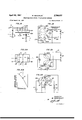
- SEMICONDUCTOR SIGNAL TRANSLATING DEVICES I1 Sheets-Sheet s has SILICON, HOLES SILICON, ELEC TRONS INTRINSIC! F R' GERMAN/UM GERMA NIUM HOLES GERMAN/UM, ELE C TRONS INTRINSIC P EOR SILICON CURRENT DENSITY (J) m/ AM/yc/w 2 FIG. 6
- FIG. I914 O I N1. 1' O N- N+ FIG. /2A- 9 1x WJ/Z 0 o FIG. /9B
- germanium may be taken, as an illustrative material, although it will be understood that the same considerations apply to others, such as other elemental semiconductors, for example silicon, and semiconductive.
- compounds for example lead sulfide, lead telluride, and copper oxide,
- the impurities' may be present in the material 7 as cast or may be added during fabrication of the material. Such semiconductors and particularly those wherein the impuritiesar'e'added are referred to commonly as doped. 'If the dominant significant'impurity, or impurities, is of the class known as donors, the free carriers normally in excess are electrons, and the material is denoted as N conductively type; if the dominant significant, impurity, or impurities, of' the lc'lass known as acceptors, the :free carriers normally 'inexcessare holes,
- the invention is not 2,790,037 Patented Apr. 23, 1957 and. the material is denoted as of P conductivity type. Conduction by extrinsic material is due primarily to the presence and flow of the carriers. introduced by impurities. A detailed exposition of the mechanisms. involved in germanium and like elemental semiconductors is found in chapter 1 of Electrons and Holes in Semi: conductors, by W. Shockley, published. 1950 by D. Van Nostrand Company, Incorporated.
- Extrinsic germanium such as is now employed in trans.- lating devices has a resistivity, at room temperature, in the range from a few ohm centimeters to a few tens of ohm centimeters, and the excess carrier densities at this temperature are of the order of, 10 per cm.
- Ideal intrinsic germanium would have a resistivity at room temperature of about ohm centimeters and essentially equal numbers of holes and electrons.
- transistors Semiconductor, e. g., germanium, devices capable of generating, amplifying, modulating, and otherwise usefully translating electrical signals now are known inthe art.
- Illustrative of such devices, which are generally referred to as transistors, are those disclosed in Patent 2,524,035, granted October 3, 1950, to J. Bardeen and W. H. Brattain and in Patent 2,569,347, granted September 25, 1951, to W. Shockley.
- These'devices involve, in general, injection of carriers into a body, or zone of a body, of extrinsic germanium or'like material, the in-' jected carriers being of the sign opposite that of those normally present in excess in the body or zone.
- the carrier injection is controlled in accordance with signals to be translated, whereby, inter alia, the conductivity of the body or zone is modulated correspondingly and amplified replicas ofthe signals are obtained in a load circuit associated with the device.
- transistors may be compared with electron discharge devices in function and performance characteristics, as is known and as discussed in some detail in Duality as a Guide in Transistor Circuit Design, by R. L. Wallace and G.
- One general object of this invention is to provide a unique class of signal translating device free from disadvantages'and limitations of presently known devices of both the electron discharge and semiconductor types.
- Another general object of this invention is to attain novel and improved performance characteristics for semiconductor signal translating devices.
- More specific objects of this invention are to extend the operating frequency range of semiconductor translators, to enhance the gain obtainable with such devices, to enable operation at'any prescribed current and current density'in a wide range, to realize operation at very high current densities, to improve the control of signals gen erated or translated, to achieve flexibility in the manner or mode of operation, to enlarge the fields of application of semiconductor signal translating devices, and to simplify the design of circuits for utilization of such devices.
- a translating device comprises a body of semiconductive material having therein a substantially intrinsic region.
- This region is of very high purity, whereby the donoracceptor unbalance is such that the resistivity of the region does not deviate more than about five percent from intrinsic. is such that the unbalance of donor and acceptor densities is less than 5.5 K/x, where x represents dimensions'of the region in centimeters, and K is the dielectric constant.
- the field density due to impurities is less than 10 volts per centimeter.
- the body has therein also, contiguous with the region, at least three zones of extrinsic material, two of the zones being of like conductivity type and the third of the opposite conductivity type, the several zones being relatively biased each at the polarity opposite that of the excess carriers therein, whereby any carriers generated in the bulk material are attracted to one or more of the zone or zones of opposite polarity.
- the thermally generated carriers in the semiconductor are swept out of the substantially intrinsic region.
- the bulk portion of the semiconductor has a lower conductivity than ideally pure or intrinsic material would have at the same temperature.
- the two zones of like conductivity are biased relative to each other so that excess carriers of the sign characteristic of these zones pass from one zone into the swept or substantially intrinsic region and flow to the other of these zones.
- the first zone will be referred to herein as the source and the second as the drain.
- the third zone that is, the one of opposite conductivity type, is utilized to control this flow of carriers between the two like zones.
- the control maybe effected in accordance with several principles or modes. Emission of carriers from the source is dependent upon the field adjacent the source, and this field is amenable'to control in accordance with the potential of the third or control zone. Also, because of the swept intrinsic character of the bulk material, the emission of carriers will set up a space charge in the bulk which may be modified by varying the potential of the drain or the control zone thereby to control the fiow of carriers from the source to the drain.
- devices constructed in accordance with this invention may involve changes of carrier density; however, in some embodiments, these changes As will be pointed out hereinafter, this region the other carriers being negligible. In these embodiments, changes in space charge occur and produce substantial changes in electric fields. These resulting fields contribute beneficially to a reduction of transit time.
- the several zones may be arrayed in several ways.
- the source and drain may be disposed on opposite faces or at opposite corners of the semiconductive body and the control zone be positioned laterally adjacent the path from source to drain, closely adjacent the source, as in the same face of the body as the source, or between the source and drain. Additional zones may be provided as described hereinafter.
- extrinsic material may be molten and cast, as in the manner disclosed in the application Serial No. 638,- 351, filed December 29, 1945, of I. H. Scaif and H. C. Theuerer, now United States Patent 2,602,211 issued July 8, 1952 whereby a segregation of impurities along an axis of the resulting ingot is produced.
- the purer portion of the ingot is then again melted, whereby a further segregation of impurities is effected. This is repeated until the final ingot or a desired portion thereof exhibits a donor-acceptor unbalance of the desired magnitude.
- the several zones may be produced in the high resistivity body by placing in contact therewith a donor or acceptor, or an alloy or mixture of the body material and a donor or acceptor, and melting the applied member thereby to develop in the resulting body an N or P zone, the N zone resulting, of course, when the applied material is a donor or donor bearing and a P zone being produced when the applied material is an acceptor or acceptor bearing.
- Indium is a typical acceptor and antimony a typical donor for germanium.
- Illustrative methods for producing a zone of N or P material are disclosed in the application Serial No. 136,038, filed December 30, 1949, of W. G. Pfann and H. C. Theuerer, now Patent 2,701,326, issued February 1, 1955 and Serial No. 271,712, filed February 15, 1952, of M. Sparks, now Patent 2,695,852, issued November 30, 1954.
- Fig. 1 is a diagram of a semiconductive body including extrinsic and substantially intrinsic zones associated as in devices constructed in accordance with this invention
- Figs. 2A and 2B are energy level diagrams for a semiconductive device including a bodyof the configuration illustrated inFig. 1;
- Figs. 3'to 12B, inclusive are diagrams and graphsv showing certain parametral relationships which Will be referred to hereinafter in the exposition of performance and designconsiderations for devices constructed in accordance with this invention
- Fig. 13 is a plan view 'of'a semiconductive element illustrative of those which may be uilized in eertain embodiments of this invention.
- Figs. 17A, 17B, and 17C are graphs depicting potential distributions in the semiconductor of Fig. 16 for certain conditions of bias of the extrinsic zones;
- Fig. 18 illustrates a triode amplifier constructed in accordance with this invention and including a control electrode between the source and drain regions;
- Fig. 19A represents a modification. of a triode depicted in Fig. 18 and each of Figs. 19B, 19C, and 19D is a graph of a characteristic of such modification;
- Fig. 20 portrays another triode illustrative of anembodiment of this invention wherein the source and control zones are arrayed in alternate relation in one face portion of a substantially intrinsic semiconductive body;
- Fig. 21A shows a tetrode constructed in accordance with this invention and including an auxiliary electrode or grid between the control electrode and the drain;
- Fig. 21B is a graph illustrating the potential distribution in the .semiconductive body of the device shown in Fig. 21A;
- Fig. 22 portrays another illustrative embodiment of this invention particularly suitable for push-pull operation
- Fig. 23 illustrates another translating device constructed in accordance with this invention and particularly suitable for the realization of current gains
- Fig. 24 shows a modification of the device illustrated in Fig. 23;
- Fig. 25 is a perspective view of a translating device embodying this invention, wherein the-control or auxiliary zone encompasses the substantially intrinsic region;
- Fig. 26 depicts a modification of the embodiment illustrated in Fig. 25 wherein the control zone includes a grid or mesh portion;
- Fig. 27 portrays another embodiment of this invention wherein the emitter, collector, and control zones are cylindrical and coaxially arrayed;
- Fig. 28 illustrates another embodiment of this invention particularly suitable for operation at relatively low emitter current densities
- Figs. 29 and 30 show still other embodiments of this invention constituting analogs of remote cut-oil or volume control types of electron discharge devices.
- zones of the semiconductive bodies illustrated are designated by the letter N. P, or I, indicative of the conductivity type thereof.
- Strongly N-type material say of the order of 0.01 ohm centimeter resistivity germanium, is designated N+
- weak N material say of the order of 40 ohm centimeter resistivity germanium
- P+ and P respectively.
- the electrodes can be classified into four groups-electron emitting, electron receiving, electron controlling, and secondary emitting surfaces.
- the cathode of a vacuum tube is generally heated, and its surface is covered by a space charge layer composed of thermionically emitted electrons. Under conditions of space charge limited emission, this space charge layer causes a maximum to occur in the potential energy versus distance curve for an electron. The current. flowing over this maximum may be calculated by statistical mechanical methods and is well approximated by Childs law (see, for example, K. T. Compton and I. Langmuir, Reviews of Modern Physics, 3, 237 (1931)).
- the analog of a thermionically emitting cathode is a body of highly doped N-typematerialin intimate contact with the space body.
- a body or simply source.
- electron sources turning later to hole sources.
- a preferred embodiment is one "in which'the space body and electron source body areportions of the same single crystal of germanium and differ only in the densities of donors and acceptors they "contain.
- An advantage of the source body over a thermionic cathode is that it is capable of far greater enrrem densit-ies per Se and requires no heat.. a a
- a body of highly doped P-type material In the neighborhood of a negative grid wire, the electric field is in such a direction as to tend to extract electrons from the grid. In the case of the analog, this field will be such as to suppress the emission of holes. Since the body is highly doped P-type, the current of electrons from it will be very small, as is well known from the theory of saturation currents from P-N junctions. (See, for example, Shockley, Electrons and Holes in Semiconductors, page 316; the saturation electron current in Equation 31 is seen to decrease with increasing conductivity u of the P-region.) A preferred form of such a grid body is again a portion of the same single crystal as the space body with proper impurity content.
- an advantage of the analogstructure is that the grid need not be negative in respect to the source in order to reduce electron current to the grid substantially to zero, whereas in a vacuum tube it must be negative.
- the reason for this difierence is that in a vacuum tube, the electrons conserve their energy and so may reach the grid if it is positive'in respect to the cathode.
- energy is lost in the conduction process and, unless the structures are comparable in size to a mean-free path, which is about 10- cm., there is no conservation of momentum of the electrons.
- biasing the grid so that the field at its surface is electron repelling over a region large enough to produce a drop of a few tenths of a volt .will suflice to prevent electron flow to the grid.
- the analog for a plate or anode is an N-type region like the source but biased so as to attract electrons. Under these conditions, it will emit a small current of holes which decreases as its impurity density increases.
- the analog of space charge due to ions is the space charge of donors and acceptors in the space body.
- the fraction of the donors and acceptors that are neutralized by electrons or holes for carrier densities of /crn. is less than one in a thousand. (See Shockley loc. cit. page 247, Fig. 10-7, and page 24.) Consequently, the space charge of the donors and acceptors remains substantially unaltered even though the carrier density varies over wide limits.
- the ion space charge may be considered as stationary and constant as the device operates. For amplifying devices and high frequency devices, this is highly advantageous compared to gas discharge tubes in which the ions change in number and location.
- This means can be used to achieve space bodies in which'the space charge canbe made to increase by large propor tions by ionization? of neutral donor electron centers.
- This ionization can be p rovoked by hot electrons, i. e., electrons whose average' energy of'motion has been in creased by the application of high'electric fields. (See Shockley, Hot Electrons in Germanium and Ohms Law, Bell System Technical Journal, 30, 990 (1951).) 1
- the transit time is expressed as a function of J and W.
- Transit time 4W /3,aV (2.101)) which shows that the transit time is 1/3 greater than for a uniform field V/ W over a distance W.
- W is eliminated from (2.1012), we obtain Transit time: !C (3V/[L) 1/3
- the I-region is supposed to be wide enough so that the central region is substantially unaffected by the ends.
- the criterion for this is that it should be many Debye Lengths wide where the Debye length is that defined by Equation'2.12 in Shockley, The Theory of p-n Junctions in Semiconductors, Bell System Technical Journal, 28, 441 (1949). In an intrinsic sample of germanium at thermal equilibrium at room temperature, the Debye length is about 6 10- cm. Where the potential begins to vary from a constant value in the middle of region I of Fig. 2A, the deviation increases by a factor of e for each Debye length.
- the physical reason for the factor of 2 is that v 'the'total density of mobile carriers is Zn, in intrinsic rna uses the volt, coulomb, and ampere for electrical .quantities and the centimeter for length.
- Space charge region arbinidsouice' Fig. 1 represents an" N4-'IN struc'ti'ire consisting of two highly doped N-regions on opposite faces of a plane parallel region of intrinsic material.
- the line terial and is substantially n in doped material. Since this ratio of n to n may be about 10- in our example, it is evident that the potential disturbance will extend only about 10* times as far into the N-region as it does into the intrinsic region.
- the solution of this equation . is readily found by standard methods (see, for example, Madelung, Die Mathematischen Hifskar des Physiker, Dover Publications, New York city,'Ne'w York; 1943, page 171, entry b of the' Table of Solutionsyor H. 11H. Piaggio, An Elementary Treatise on Differential Equations end Their Applications, G.
- the product -E,u is simply the drift velocity towards increasing x.
- the first term therefore, represents simply the charge density necessary to carry the current I by drift.
- the term with const carries no current and represents a distribution of electrons in thermal equilibrium. Such a distribution should not be present in appreciable concentration until the abrupt potential drop ceases, as, for example, at the right edge of Fig. 23. From this reasoning, we conclude that const must be very small, so that it becomes comparable to J/(-E,) In fact, if we assume that at the right edge of Fig.
- the const term accounts for the entire density n then at 0.5 volt above the N-region on the right, the density is less by a factor of 3X10 and at one volt it is lessby 10 From this, it is evident that the const term is negligible throughout the major part of the middle region.
- the value of 11(0) may be expressed in terms of the rise in the potential maximum above the Fermi level in the N-region.
- the factor of A) comes from the approximation that 1(0) /2 )lm.
- the current is carried primarily by drift as soon as a point with a potential energy drop of kT is reached, only 24 percent of the current being carried by diffusion.
- the relationship of current to density at the maximum for the parabolic approximation at the maximum is found by solving for J in the expression for qnin terms 'ofJ/D, etc. Thisgives a value slightly larger than the crude estimate of qDn(0)/L given in Equation 3.17.
- the carrier density may be as high as 10 (run-* corresponding to a charge density of 1.6 coulombs/cm. This charge density corresponds to a current density of 7x10 amperes/cm. From this it is evident that currents enormously larger than thermionic currents can be drawn from the cathodes of the analog-structures before the potential maximum corresponding to space charge limited emission is wiped out and the field reaches directly into the N-type emitter body.
- Equation 5.9 The quantity p is a simplified form of Equation 5.9:
- a third quantity of interest is Qa'which is approximately the amount of charge per unit area within 'a layer L:
- Structures of controlled distribution of lifetime can be formed in various ways. For example, it is known that heat treatment produces centers that aid recombination and so does bombardment by nuclear particles (see Shockley, Electrons and Holes in Semiconductors, page 347). It has also been established that nickel is very eifective in reducing lifetime. The addition of 1 milligram of nickel to a 100 gram melt of germanium reduces lifetime to a few microseconds or less in mate rial that would otherwise be hundreds or thousands of microseconds. By this technique, an ingot with a sharp boundary between long and short lifetime may be formed.
- nickel may be diffused in from the surface.
- the holes are distributed in this region in proportion to the ordimates of Fig. 4 and for the assumption of parabolic potential, 84 percent of the holes lie between +L and L.
- the charge per unit area of electrons in this region will be of the order of magnitude of Qr introduced in Section VI by Equation 6.6. If qP exceeds this value by a large factor, then the space charge of holes will have a major influence on the potential distribution.
- Fig. 11A we represent the N+IN+ structure and by the shape .of the potential energy curves of Fig. 11B, we indicate that it is wide compared to a Debye length. If this is not the case, 11(0) will be large compared to m, and the situation is not one of the class we are considering.
- Fig. 11C we represent the condition with a moderate applied potential. It is to be noted that:
- n1W is however, bstieiiactlyfth numberpfi holes in theintrinsic case. 'Ihis' e'st'ablishes the": o fr f e" ion (1) 'For the "cases ofi erestiin' this the 'width of the stagnant" region wilY'be less t n W bya factor cc, as represented in Fig. 1'1.
- Iheratio of the charge qP of the holes to .Qr is a measure of the strength of the stagnant region. It may be expressed in terms of the ratio of aW to has follows: j
Landscapes
- Engineering & Computer Science (AREA)
- Power Engineering (AREA)
- Physics & Mathematics (AREA)
- Condensed Matter Physics & Semiconductors (AREA)
- General Physics & Mathematics (AREA)
- Computer Hardware Design (AREA)
- Microelectronics & Electronic Packaging (AREA)
- Bipolar Transistors (AREA)
Description
April 23, 1957 w/sHocKLEY 7 2,790,037
' SEMICONDUCTOR srcum. TRANSLATING DEVICES Filed March 14, 1952 11 Sheets-Sheet 1 1 FIG.
J 4. I J- N 7 f N 556 5369 @eeaea N. FIG. 28
7 /NVENTOR I K W SHOCK/.5)
. .BVM
L v ATTORNEK April 23', 1957 w. SHOCKLEY 2,790,037
SEMICONDUCTOR SIGNAL TRANSLATING DEVICES Filed March 14, 1952 11 She'etS-Sheet 2 POTENTIAL ENERGY FOR AN ammo/v /N l/E N 7' OP w SHOCKLE) ATTORNEK- April 23,
Filed March 14 1952 MB/CM 3 Y a a, i u
CHARGE DEM/TY (Pr) COULO 8 1957 w. SHOCKLEY I 2,790,037
SEMICONDUCTOR SIGNAL TRANSLATING DEVICES I1 Sheets-Sheet s has SILICON, HOLES SILICON, ELEC TRONS INTRINSIC! F R' GERMAN/UM GERMA NIUM HOLES GERMAN/UM, ELE C TRONS INTRINSIC P EOR SILICON CURRENT DENSITY (J) m/ AM/yc/w 2 FIG. 6
GERMAN/UM, HOLES ERMA N/UM, E LE C TRONS SILICON, HOLES SILICON, EL scmo/vs -3 -2 2 8 /o /q /o 10 I02 10 I0 CURRENT DENSITY //v AMP/CM OR W SHOCK L E Y A rrok/va'v April 23, 195 7 W Filed March 14, 1952 POTENTIAL //v vans,
REVERSE BIAS POTENTIAL IN VOLTS, V
W. SHOCKLEY SEMICONDUCTOR SIGNAL TRANSLATING DEVICES /0' lo' 3 10' l0" l0 l0 2 lo /0 CURRENT DENSITY (J) //v AMP/6M2 FIG. /0
BARR/ER WIDTH IN CM co/vs TANT CON- -L/NES 0F CONSTANT MAX. I F/[LD //v VOLT CM 11 Sheets-Sheet 5 /0 l0 2 l0 /0 2 I0 /0 9 CAPACITANCE //v MME/CM v v N VE N TOP W 5 HOC K L E) ATTORNEY P 2 1957 w. SHOCKLE'Y 2,790,037
SEMICONDUCTOR SIGNAL TRANSLATING DEVICES Filed March 14, $952 11 Sheets-Sheet 6 FIG. //A
. o( w STAGNANT 3,53 ,95 1
FIG/IC v INVENTOR W SHOCKLEY I Byaw ATTORNEY April 23, 1957 w. SHOCKLEY 2,790,037
SEMICONDUCTOR SIGNAL TRANSLATING DEVICES Filed March 14, 1952 ll Sheets-Sheet '7 F IG ./3
N ZR N Fla. /4
COOL/N6 F/N FIG. l5-
. lNl/ENTOR W. SHOCKLEY A TTOPNEV P 9 w. SHOCKLEY 2,790,037
SEMICONDUCTOR SIGNAL TRANSLATING DEVICES Filed March 14, 1952 11 Sheets-Sheet 9 FIG. I914 O I N1. 1' O N- N+ FIG. /2A- 9 1x WJ/Z 0 o FIG. /9B
POTENTIAL ENERGY 0F ELECTRONS FIG. I28
o v :E 2 55 a; u Q's E3 (P=n E SOLUTION) \IU E1. F/G. I90 I a Y Eg lam s INVENTOR A W' SHOCKLEY BY Y% a: v a? ATTORNEY.
SEMICONDUCTOR SIGNAL .TRANSLATING.
DEVICES: 7
William Shockley, Madison, N. J., assignor to Bell Telephone Laboratories, Incorporated, New York, N. Y., a corporationof New-York- Application March 14, 1952, Serial No. 276,511
1 Claims; c1.-.179-171 nited States Patent of electron discharge devices and, more specifically, I
vacuum. tubes. Such devices, despite their manifest utility and widespread utilizationphave definite limitations and practical disadvantages; Among these are fragility, limited useful life, and necessity for filament or heater power supplies. Additionally, and these factors are of particular moment from performance standpoints, electron discharge devices suffer from limitations in the current densities that can be realized practically from the emitter or cathode and in the potentials which can be employed on the control electrode or grid without the latter drawing a substantial amount of current. Further, in electron discharge devices, an inherent and ever pres ent problem arises by virtue of space charge. Operation of such devices entails control or neutralization of space charge, but the mechanisms available are restricted for practical purposes. For example, electron space charge may be neutralized through the use of a gas and attendant space charge of ions. However, ionic space charge introduces deleterious elfects such as noise, time delay, and variability.
Some of the disadvantages and limitations of electron discharge devices have been overcome by the advent of semiconductor devices. g
Before discussing such devices, it maybe advantageous to review some of the salient characteristics of semiconductive materials and the principles and phenomena involved in electrical conduction thereby. For this purpose, germanium may be taken, as an illustrative material, although it will be understood that the same considerations apply to others, such as other elemental semiconductors, for example silicon, and semiconductive. compounds, for example lead sulfide, lead telluride, and copper oxide,
cess in the material of eithe'rofttwo types of electrical carriers. The impurities'may be present in the material 7 as cast or may be added during fabrication of the material. Such semiconductors and particularly those wherein the impuritiesar'e'added are referred to commonly as doped. 'If the dominant significant'impurity, or impurities, is of the class known as donors, the free carriers normally in excess are electrons, and the material is denoted as N conductively type; if the dominant significant, impurity, or impurities, of' the lc'lass known as acceptors, the :free carriers normally 'inexcessare holes,
and that in its broader aspects, the invention is not 2,790,037 Patented Apr. 23, 1957 and. the material is denoted as of P conductivity type. Conduction by extrinsic material is due primarily to the presence and flow of the carriers. introduced by impurities. A detailed exposition of the mechanisms. involved in germanium and like elemental semiconductors is found in chapter 1 of Electrons and Holes in Semi: conductors, by W. Shockley, published. 1950 by D. Van Nostrand Company, Incorporated.
Extrinsic germanium such as is now employed in trans.- lating devices has a resistivity, at room temperature, in the range from a few ohm centimeters to a few tens of ohm centimeters, and the excess carrier densities at this temperature are of the order of, 10 per cm. Ideal intrinsic germanium would have a resistivity at room temperature of about ohm centimeters and essentially equal numbers of holes and electrons.
Semiconductor, e. g., germanium, devices capable of generating, amplifying, modulating, and otherwise usefully translating electrical signals now are known inthe art. Illustrative of such devices, which are generally referred to as transistors, are those disclosed in Patent 2,524,035, granted October 3, 1950, to J. Bardeen and W. H. Brattain and in Patent 2,569,347, granted September 25, 1951, to W. Shockley. These'devices involve, in general, injection of carriers into a body, or zone of a body, of extrinsic germanium or'like material, the in-' jected carriers being of the sign opposite that of those normally present in excess in the body or zone. The carrier injection is controlled in accordance with signals to be translated, whereby, inter alia, the conductivity of the body or zone is modulated correspondingly and amplified replicas ofthe signals are obtained in a load circuit associated with the device. A limitation upon the performance of. such devices, specifically the upper frequency of the operating range, results from the finite transit times of the carriers involved in the conduction process, Also, in general, and particularly in point con tactdevices, unless special constructional features are introduced, the current gain realizable is relatively small. Further, although transistors may be compared with electron discharge devices in function and performance characteristics, as is known and as discussed in some detail in Duality as a Guide in Transistor Circuit Design, by R. L. Wallace and G. Raisbeck, Bell System Technical Journal, April 1951, page 381, and in W. Shockley, loc. cit., pages 92-95, the two are not strictly analogs. Thus, in some applications, substantial alteration in configuration and design of known electrondis charge device circuitry is necessary to utilize transistors for like purposes.
Improved performance from the standpoint of frequency range of operation of semiconductor translator devices of presently known types can be achieved through operation of the device so that a space charge region is established in the semiconductive body, as disclosed,
for example, in the application Serial No. 243,541, filed August 24, 1951, of w. Shockley, now Patent 2,744,970, issued May 8,1956. Establishment of such space charge region, however, entails the'use. of fairly high voltages and, further, the region is of'lirnited extent. improved performance from the standpoint of current gainmay be realized, as disclosed in the application Seri al No. 237,746, filed July 20, 1951, of W. W; van Roosbroeck, by utilizing a body of highly purified materialwherein theexcess carrier concentrations are small or one wherein electron-hole pairs are generated in such profusion that efiectively the two kinds-of carriers are insubstantial equality. The conductivity of the body and hence the current flow between two metallic connecti is thereto is controlled by injecting carriers of oneortlie othef sign, as by way ofa point contact bearing against t body. Such devices, in" general, require relatively high current densities for satisfactory operation and operate upon the principle of conductivity modulation of regions in which the space charge is substantially zero. Also, current gain increase is realized at the expense of frequency range of operation.
One general object of this invention is to provide a unique class of signal translating device free from disadvantages'and limitations of presently known devices of both the electron discharge and semiconductor types.
Another general object of this invention is to attain novel and improved performance characteristics for semiconductor signal translating devices.
More specific objects of this invention are to extend the operating frequency range of semiconductor translators, to enhance the gain obtainable with such devices, to enable operation at'any prescribed current and current density'in a wide range, to realize operation at very high current densities, to improve the control of signals gen erated or translated, to achieve flexibility in the manner or mode of operation, to enlarge the fields of application of semiconductor signal translating devices, and to simplify the design of circuits for utilization of such devices.
In one illustrative embodiment of this invention, a translating device comprises a body of semiconductive material having therein a substantially intrinsic region. This region is of very high purity, whereby the donoracceptor unbalance is such that the resistivity of the region does not deviate more than about five percent from intrinsic. is such that the unbalance of donor and acceptor densities is less than 5.5 K/x, where x represents dimensions'of the region in centimeters, and K is the dielectric constant. The field density due to impurities is less than 10 volts per centimeter.
The body has therein also, contiguous with the region, at least three zones of extrinsic material, two of the zones being of like conductivity type and the third of the opposite conductivity type, the several zones being relatively biased each at the polarity opposite that of the excess carriers therein, whereby any carriers generated in the bulk material are attracted to one or more of the zone or zones of opposite polarity.
Thus, the thermally generated carriers in the semiconductor are swept out of the substantially intrinsic region. Under these conditions, the bulk portion of the semiconductor has a lower conductivity than ideally pure or intrinsic material would have at the same temperature.
The two zones of like conductivity are biased relative to each other so that excess carriers of the sign characteristic of these zones pass from one zone into the swept or substantially intrinsic region and flow to the other of these zones. For ease of discussion, the first zone will be referred to herein as the source and the second as the drain. The third zone, that is, the one of opposite conductivity type, is utilized to control this flow of carriers between the two like zones.
The control maybe effected in accordance with several principles or modes. Emission of carriers from the source is dependent upon the field adjacent the source, and this field is amenable'to control in accordance with the potential of the third or control zone. Also, because of the swept intrinsic character of the bulk material, the emission of carriers will set up a space charge in the bulk which may be modified by varying the potential of the drain or the control zone thereby to control the fiow of carriers from the source to the drain.
.Two major principles of devices constructed in accordance with this invention are to be noted especially, to wit, thefsubstantial denuding of the bulk material of carriersgenerated therein, as by thermal effects, and the control of flow of carriers from the source and into the bulk materialby either a field efiect or space charge control, or both. e Y
It may be noted that devices constructed in accordance with this invention may involve changes of carrier density; however, in some embodiments, these changes As will be pointed out hereinafter, this region the other carriers being negligible. In these embodiments, changes in space charge occur and produce substantial changes in electric fields. These resulting fields contribute beneficially to a reduction of transit time.
The several zones may be arrayed in several ways. For example, the source and drain may be disposed on opposite faces or at opposite corners of the semiconductive body and the control zone be positioned laterally adjacent the path from source to drain, closely adjacent the source, as in the same face of the body as the source, or between the source and drain. Additional zones may be provided as described hereinafter.
Material suitable for use in devices constructed in accordance with this invention may be produced by successive purification of extrinsic semiconductors. For example, extrinsic material may be molten and cast, as in the manner disclosed in the application Serial No. 638,- 351, filed December 29, 1945, of I. H. Scaif and H. C. Theuerer, now United States Patent 2,602,211 issued July 8, 1952 whereby a segregation of impurities along an axis of the resulting ingot is produced. The purer portion of the ingot is then again melted, whereby a further segregation of impurities is effected. This is repeated until the final ingot or a desired portion thereof exhibits a donor-acceptor unbalance of the desired magnitude. This unbalance maybe determined in the manners indicated in Shockley, Electrons and Holes in Semiconductors, section 1.3, and G. L. Pearson and J. Bardeen, Physical Review 75, 865. Advantageously, single crystal material is employed. Such material may be'produced in the manner described in the application Serial No. 234,- 408, filed June 29, 1951, of E. Buehler and G. K. Teal.
The several zones may be produced in the high resistivity body by placing in contact therewith a donor or acceptor, or an alloy or mixture of the body material and a donor or acceptor, and melting the applied member thereby to develop in the resulting body an N or P zone, the N zone resulting, of course, when the applied material is a donor or donor bearing and a P zone being produced when the applied material is an acceptor or acceptor bearing. Indium is a typical acceptor and antimony a typical donor for germanium. Illustrative methods for producing a zone of N or P material are disclosed in the application Serial No. 136,038, filed December 30, 1949, of W. G. Pfann and H. C. Theuerer, now Patent 2,701,326, issued February 1, 1955 and Serial No. 271,712, filed February 15, 1952, of M. Sparks, now Patent 2,695,852, issued November 30, 1954.
The invention and the several features thereof will be understood more clearly and fully from the following detailed description with reference to the accompanying drawing, in which:
Fig. 1 is a diagram of a semiconductive body including extrinsic and substantially intrinsic zones associated as in devices constructed in accordance with this invention;
Figs. 2A and 2B are energy level diagrams for a semiconductive device including a bodyof the configuration illustrated inFig. 1;
Figs. 3'to 12B, inclusive, are diagrams and graphsv showing certain parametral relationships which Will be referred to hereinafter in the exposition of performance and designconsiderations for devices constructed in accordance with this invention;
Fig. 13 is a plan view 'of'a semiconductive element illustrative of those which may be uilized in eertain embodiments of this invention;
lating device illustrative of one embodiment of this invention;
Figs. 17A, 17B, and 17C are graphs depicting potential distributions in the semiconductor of Fig. 16 for certain conditions of bias of the extrinsic zones;
Fig. 18 illustrates a triode amplifier constructed in accordance with this invention and including a control electrode between the source and drain regions;
Fig. 19A represents a modification. of a triode depicted in Fig. 18 and each of Figs. 19B, 19C, and 19D is a graph of a characteristic of such modification;
Fig. 20 portrays another triode illustrative of anembodiment of this invention wherein the source and control zones are arrayed in alternate relation in one face portion of a substantially intrinsic semiconductive body; Fig. 21A shows a tetrode constructed in accordance with this invention and including an auxiliary electrode or grid between the control electrode and the drain;
Fig. 21B is a graph illustrating the potential distribution in the .semiconductive body of the device shown in Fig. 21A;
Fig. 22 portrays another illustrative embodiment of this invention particularly suitable for push-pull operation;
Fig. 23 illustrates another translating device constructed in accordance with this invention and particularly suitable for the realization of current gains;
Fig. 24 shows a modification of the device illustrated in Fig. 23;
Fig. 25 is a perspective view of a translating device embodying this invention, wherein the-control or auxiliary zone encompasses the substantially intrinsic region;
Fig. 26 depicts a modification of the embodiment illustrated in Fig. 25 wherein the control zone includes a grid or mesh portion;
Fig. 27 portrays another embodiment of this invention wherein the emitter, collector, and control zones are cylindrical and coaxially arrayed;
Fig. 28 illustrates another embodiment of this invention particularly suitable for operation at relatively low emitter current densities; and
Figs. 29 and 30 show still other embodiments of this invention constituting analogs of remote cut-oil or volume control types of electron discharge devices.
It may be noted that in the drawing, zones of the semiconductive bodies illustrated are designated by the letter N. P, or I, indicative of the conductivity type thereof. Strongly N-type material, say of the order of 0.01 ohm centimeter resistivity germanium, is designated N+, and weak N material, say of the order of 40 ohm centimeter resistivity germanium, is designated N-. Similarly, strong and weak P-type material, say of the order of 0.91 ohm centimeter and 40 ohm centimeter resistivity germanium, is designated P+ and P respectively.
Full understanding of the invention, appreciation of the several features thereof, and construction of devices in accordance therewith will be facilitated by a detailed b=ratio of electron to hole mobility C=capacitance per unit area or simply capacitance ,D=diffusion constant for thermal motion of holes or electrons 'e=2.73=base of naperian logarithms E=electric field f frequency J=current density k=Boltzmanns constant L'1=see Section VI 1 m fnass of free electron -a;=defined in Section VI 1z=dielectrie constant =resistivity, also charge density p =see Section VI a=conductivity r= a life time or diffusion time r =see Section VI I. Some basic principles for analog-structure design It may be helpful in understanding the principles of devices embodying this invention to compare the structures and principles with those of vacuum tubes. In many vacuum tubes, the electrodes can be classified into four groups-electron emitting, electron receiving, electron controlling, and secondary emitting surfaces. The cathode of a vacuum tube is generally heated, and its surface is covered by a space charge layer composed of thermionically emitted electrons. Under conditions of space charge limited emission, this space charge layer causes a maximum to occur in the potential energy versus distance curve for an electron. The current. flowing over this maximum may be calculated by statistical mechanical methods and is well approximated by Childs law (see, for example, K. T. Compton and I. Langmuir, Reviews of Modern Physics, 3, 237 (1931)). The distribution of potential in the volume beyond the space charge layer is determined by the boundary values and by the space charge produced by the electrons themselves. Except for I cases involving secondary emission, no other sources of current or space charge are present in the'tube. If some gas is present, a space charge of ions may arise. This space charge tends to cancel that of the electrons and below criteria for estimating whether the impurities will have major or minor influence upon the behavior of the device. We shall refer to. this material as the space body. V I
The analog of a thermionically emitting cathodeis a body of highly doped N-typematerialin intimate contact with the space body. We shall refer to such a body as a source body or simply source. We shall initially deal with electron sources, turning later to hole sources. A preferred embodiment is one "in which'the space body and electron source body areportions of the same single crystal of germanium and differ only in the densities of donors and acceptors they "contain. An advantage of the source body over a thermionic cathode is that it is capable of far greater enrrem densit-ies per Se and requires no heat.. a a
a body of highly doped P-type material. In the neighborhood of a negative grid wire, the electric field is in such a direction as to tend to extract electrons from the grid. In the case of the analog, this field will be such as to suppress the emission of holes. Since the body is highly doped P-type, the current of electrons from it will be very small, as is well known from the theory of saturation currents from P-N junctions. (See, for example, Shockley, Electrons and Holes in Semiconductors, page 316; the saturation electron current in Equation 31 is seen to decrease with increasing conductivity u of the P-region.) A preferred form of such a grid body is again a portion of the same single crystal as the space body with proper impurity content.
It should be noted that an advantage of the analogstructure is that the grid need not be negative in respect to the source in order to reduce electron current to the grid substantially to zero, whereas in a vacuum tube it must be negative. The reason for this difierence is that in a vacuum tube, the electrons conserve their energy and so may reach the grid if it is positive'in respect to the cathode. In the analog-structure, energy is lost in the conduction process and, unless the structures are comparable in size to a mean-free path, which is about 10- cm., there is no conservation of momentum of the electrons. Hence, in such structure biasing the grid so that the field at its surface is electron repelling over a region large enough to produce a drop of a few tenths of a volt .will suflice to prevent electron flow to the grid.
The analog for a plate or anode is an N-type region like the source but biased so as to attract electrons. Under these conditions, it will emit a small current of holes which decreases as its impurity density increases.
The analog of space charge due to ions is the space charge of donors and acceptors in the space body. In germanium at room temperature, the fraction of the donors and acceptors that are neutralized by electrons or holes for carrier densities of /crn. is less than one in a thousand. (See Shockley loc. cit. page 247, Fig. 10-7, and page 24.) Consequently, the space charge of the donors and acceptors remains substantially unaltered even though the carrier density varies over wide limits. As a result, the ion space charge may be considered as stationary and constant as the device operates. For amplifying devices and high frequency devices, this is highly advantageous compared to gas discharge tubes in which the ions change in number and location.
In silicon, on the other hand, a significant fraction of the electrons in an N-type sample may be bound to donors at room temperature. (See Shockley loc. cit. page 15 and Fig. 1-9 and also Fig. 1-12.) Changes in the number of electrons bound to donors result in changes in the ionic space charge and may be used to simulate efiects of changing ion densities in gas discharge tubes. It should be pointed out that this eifect can be enhanced by using large concentrations of donors and acceptors in approximate compensation. Under these conditions, the density of electrons required to neutralize an N-type sample will be Nd-Na; if Na is made larger while keeping Nd,Na constant, it is evident that the fraction of electrons bound to donors will beincreased. This means can be used to achieve space bodies in which'the space charge canbe made to increase by large propor tions by ionization? of neutral donor electron centers. This ionization can be p rovoked by hot electrons, i. e., electrons whose average' energy of'motion has been in creased by the application of high'electric fields. (See Shockley, Hot Electrons in Germanium and Ohms Law, Bell System Technical Journal, 30, 990 (1951).) 1
In the analogs-discussed above, emphasis has been placed uponelectrons as the active carriers. ',It is evident that similar analogs can, be discussed inwhich holes are active simply by interchanging, the? roles of donors and acceptors and reversing the signs of voltages and currents.
II. The analog of Childs law We shall next consider some quantitative relationships that may be used for designing structures embodying various features of this invention. The first of these is the analog for Childs law. Childs law is derived by assuming that the field and potential at the cathode are zero, the current density is J, the space charge is p, and the velocity of motion is v= /2qV/m (2.1)
where V is the voltage through which the electrons have fallen. The current density is This leads to Poissons equation in MKS units in the form This equation, which we have written without regard to sign, can be integrated to give Where x is the distance from cathode to anode plane.
For the analog equation, we shall suppose that we are dealing with electrons so that their charge density has a negative sign, and the potential V (x) increases from x=0 Where the field is zero to positive values for x 0. The drift velocity is to the right and is given by v=,udV/dx (2.5)
in writing this expression, we tacitly ignore the elfects of diffusion. This is the analog of neglecting the thermal velocity distribution in Childs law. We return to this point below. The charge density is then where J is the absolute value of current density, the current being in the direction of decreasing x. Poissons equation with due regard to sign is Kgd V/d-l7 p=J/U=J+H (2.7)
In this form, the transit time is expressed as a function of J and W. Using (2.9) to eliminate J leads to Transit time=4W /3,aV (2.101)) which shows that the transit time is 1/3 greater than for a uniform field V/ W over a distance W. If W is eliminated from (2.1012), we obtain Transit time: !C (3V/[L) 1/3 The magnitude of the electric field at x=W is dV/dx=3V/ 2W =(3]V/Ice ;l)1/3 (2.11)
We shall present numerical values for (2.10) and (2.11) in Section VI.
For germanium, we have K=16 ==0.36m. /volts sec.
It is instructive to compare this with Childfs 'law, which is so tha The comparison is best made in-termsofthe formulae in MKS units and gives In this form, the ratio is seen to be about one fortieth times the ratio of the velocity of an electron in free space with kinetic energy eV and the velocity of an electron drifting in germaniumundenaheldV/x. Drift velocities of to 10" cm./sec. have been observed in germanium (see Shockley, Hot ElectronsinGermanium and Ohms Law, Bell System Technical Journal, .30, 990 (1951)). For these high velocities, dependence of mobility upon electric field modifies the above analysis somewhat. In estimating the ratio of currents, however, we .may take v=10 cm./ sec. as an example. For equality of the currents, the Childs law .velocity'must be 4x10 cm./sec., which corresponds to voltage of about 0.4 .volt. From this we see that for geometrically similar structures, the Childs law current will exceed the analog current for applied voltages greater than.about.0.4 volt. .At 40 volts,
the ratio would be 10. I
This relationship is not particularly significant, however, because Childs law devices are more generally limited by the limited emission from the cathode. This limitation is much less severe in the analog-structures, as
we shall change to a system of units more convenient for our purposes than the MKS units. This system of units, referred to as the L system in Shockley loc. cit. page 213,
greater than 10 cm.- so that the electron gases therein were. degenerate. The I-region is supposed to be wide enough so that the central region is substantially unaffected by the ends. The criterion for this is that it should be many Debye Lengths wide where the Debye length is that defined by Equation'2.12 in Shockley, The Theory of p-n Junctions in Semiconductors, Bell System Technical Journal, 28, 441 (1949). In an intrinsic sample of germanium at thermal equilibrium at room temperature, the Debye length is about 6 10- cm. Where the potential begins to vary from a constant value in the middle of region I of Fig. 2A, the deviation increases by a factor of e for each Debye length. When the deviation in potential exceeds kT/q=( .1 volt, the rate of increase is even faster. Thus, the deviation from a small fraction of (kT/q) up to the maximum value shown in this figure for the intrinsic material will occur in less than 10' cm.
In the N+-region, the efiective Debye length is less by a factor (2n /n' as may be seen from the text following Equation 2.13 of the reference, letting n =the density of electrons in the intrinsic materialand n that in the 'N-region. The physical reason for the factor of 2 is that v 'the'total density of mobile carriers is Zn, in intrinsic rna uses the volt, coulomb, and ampere for electrical .quantities and the centimeter for length. In this system, the permitivity of free space is denoted by V 6 =s.ss 10 farads/cml- 2.17 In these units, Poissons equation is formally the same as in the'MKS and is p xe d V/dx' p v (2.1 8) where p is the charge density in coulombs/cmfi. The current density is J=p,u,E (2.19) with all quantities expressed in the L" system. In the L system, all the equations for semiconductors have the same form as those derived above and take on the correct values if s is replaced by EL. The current for the Childs law analog becomes r J=5.7 5 10- V /r amp/cm? (2.20) The same procedure cannot beca rri ed outfor Childfs'law, since mechanical units and electrical'unitsof energy are not consistent in the L system; HoweveriChilds "law may be directly transformed from Equation 2.14 and becomes J,=,2.33 0gw/'-{;z gala/ems 2.2 1 the numerical coefiicient being the same in the two systems.
111. Space charge region arbinidsouice' Fig. 1 represents an" N4-'IN struc'ti'ire consisting of two highly doped N-regions on opposite faces of a plane parallel region of intrinsic material. In Fig. 2A, the line terial and is substantially n in doped material. Since this ratio of n to n may be about 10- in our example, it is evident that the potential disturbance will extend only about 10* times as far into the N-region as it does into the intrinsic region.
Let us next suppose a potential is applied so that electron flow to the right is produced. The potential distribution will then assume the form shown in Fig. 2B, the imref or quasi-Fermi level for'electrons (defined in Shockley, Sparks, and Teal in the Physical Review 83, 151 (1951) and Shockley, Electrons and Holes in Semiconductors, page 308) being shown. Although it is possible to determine the potential distribution, electron and hole densities and currents from the system of non-linear differential equations appropriate to this figure, the physical insight necessary to apply the features of this invention may be more readily grasped bya simpler procedure. For this purpose, we consider Fig. 3.
, This figure represents a potential energy distribution similar to. Fig. 2B. Howeve 'we do not specify what so designated represents'theFe'r'mi-level and is drawn as 1 distribution of charges produces this potential distribution "V(x). We shall next assume that V(x) isaknown function of x and shall calculate the electron density. The equation for current density J from right to left is:
(Equation 3.1 isfdiscussed in ShdckleyQElectrons and Holes in Semiconductors, page 299, Equation 1b; the signs are diiferent since, by definition, I is current to right and J is current to left and E,=dV/dx..) The solution of this equation .is readily found by standard methods (see, for example, Madelung, Die Mathematischen Hifsmittel des Physiker, Dover Publications, New York city,'Ne'w York; 1943, page 171, entry b of the' Table of Solutionsyor H. 11H. Piaggio, An Elementary Treatise on Differential Equations end Their Applications, G. jBell and Sons, Ltd., London 1929, page 17; or other standard texts) andrnay be expressed formally as 7 t vtei-wztrm a1 orn and may suppose thefomittd terms are relatively small hill.
over a range in which V(x) increases by many times kT/q. Inserting this in the integral leads to qn(x,)=(J/D) (kT/qE,) +const ex-p(qV(x,)/kT) =J/(E,) +const exp(qV(x,) /kT) (3.4)
In this expression, the product -E,u is simply the drift velocity towards increasing x. The first term, therefore, represents simply the charge density necessary to carry the current I by drift. The term with const carries no current and represents a distribution of electrons in thermal equilibrium. Such a distribution should not be present in appreciable concentration until the abrupt potential drop ceases, as, for example, at the right edge of Fig. 23. From this reasoning, we conclude that const must be very small, so that it becomes comparable to J/(-E,) In fact, if we assume that at the right edge of Fig. 2B, the const term accounts for the entire density n then at 0.5 volt above the N-region on the right, the density is less by a factor of 3X10 and at one volt it is lessby 10 From this, it is evident that the const term is negligible throughout the major part of the middle region.
The same reasoning indicates that the exact choice of the upper limit in the integral term is unimportant. A convenient choice may be taken as some point in the N- region on the right. An exact choice can be made which will lead to a proper allowance for the ohmic drop due to electron current in this region. Since the steps are somewhat tedious and add little to the physical picture, however, we shall not burden the exposition with them.
Accordingly, we shall take our solution as From the consideration of certain general features of I(x), important semiquantitative conclusions can be reached about the relationships between n(x), J, and a quantity L defined below.
The integrand in I(x) .is evidently a bell shaped func tion of y as represented in Fig. 4 with its maximum at x= where the maximum in the potential energy of Fig. 3 L
The value of the integral when x=2c may be corresponding to current flow entirely by drift.
Let us next consider the region to the left of x: --L. In this region, the integral I(x) has nearly its limiting value denoted by Im. In this region, therefore,
To the degree that 1111 is a good approximation to I, this represents the Boltzmann or thermal equilibrium distribution of electrons. Since 1111 is a good approximation to I(x) for x --L, it is evident that withdrawal of electrons to form the current I does not disturb the dis tribution of electrons markedly beyond a potential energy drop of kT below the maximum. An electron at kT' below the maximum has only about one chance in e of getting over the maximum as compared to drifting down not disturbed much by electron loss.
As a result, the electrondistribution at x=-L is J: Dqdn/dx (3.9)
so that the value of dn/dx is dn/dx= J/qD 3.10
The value of n(0) itself may be estimated by taking I(0)=Lexp[qV(0)/kT] 3.11 i. e., by assuming the integral is equal to the peak value of the integrand times a distance L. By virtue of the cancellation of the exponentials in (3.5), this gives qn(0) JL /D (3.12
which leads to In Section IV, an exact expression will be derived for a particular potential distribution.
The value of 11(0) may be expressed in terms of the rise in the potential maximum above the Fermi level in the N-region. On this basis, we have n(0)=%Nexpq[V(O)-VF]/kT (3.14) where q[Vr V(0)] is the energy above the Fermi level of an electron at rest at x=0. (See Electrons and Holes in Semiconductors, page 240, Equation 11, and page 308, Equation 18.) The factor of A) comes from the approximation that 1(0) /2 )lm.
Putting this value of n(0) in the expression for current gives J=(qDNc/2L)exp{q[ V(0)VF]/kT} (3.15) From this it follows that changes in height of V(0) which do change L change the current density at a rate corresponding to a conductance per unit area equal to current density J divided by voltage kT/q. (In passing, we note that differentiating the Childs law analog gives a much smaller conductance of 21/ V when V is large compared to kT/q.)
IV. The parabolic potential approximation In order to make the above theory somewhat morc quantitative, we shall assume that near the maximum we may write V(x) in the form The integrals referred to then are expressible in terms of the error function or probability integral, and we have The current carried by drift at x=+L may be calculated. At x=+L, the field is E=-dV/dx= -2kT/qL (4.7)
and the drift current is J (drift) -qn .tE 4.8) (ZukT/qL) (J/D)exp{ [qV() lkT] +1}1(L)- =(J/L)e(L1r -0.1577 p =0.76J 4.9)
Thus, the current is carried primarily by drift as soon as a point with a potential energy drop of kT is reached, only 24 percent of the current being carried by diffusion. The relationship of current to density at the maximum for the parabolic approximation at the maximum is found by solving for J in the expression for qnin terms 'ofJ/D, etc. Thisgives a value slightly larger than the crude estimate of qDn(0)/L given in Equation 3.17.
V. The self charge approximation The quantity 17 occurs frequently in the theory, and we give its values for several casesin Section VI.
if the space charge is produced by the electrons themselves, the potential will not be accurately quadratic since the space charge dies away rapidly to the right and builds up rapidly to the left 'of the maximum. For purposes of estimating orders of magnitude which suffice for many design purposes, however, we may assume that the space charge is substantially uniform over-a region lying within kT of energy of 'themaximum. We may then take for L the value L=[2n/qn(0)] (5.5)
Inserting this value into the Expression 4.10- for the current, we have I J=(2/1 )Dqn(0)/L p( U 0 v where (0) is the charge density of the electrons at p 0 =q 1 0i 1)- Since 71 0 varies asexp q[V( 0)' VFl/kT, the conductance over'the maximum for this case of space charge due to the electrons themselves is dJ/dI 0 =3 J/2kr (5.8) an expression (3/2) as large as (3.16) in. which L was assumed independent of V(O) the equation for J can be solvedfor (0)=qn(0) euro- 1 coulomb/0111. 5.9
14 for D=90 cmfi/sec. corresponding to electrons in germanium. Thisequation may be solved for J:
]=3.5 10 p amp/cm. (5.10)
In heavily doped N-type germanium, the carrier density may be as high as 10 (run-* corresponding to a charge density of 1.6 coulombs/cm. This charge density corresponds to a current density of 7x10 amperes/cm. From this it is evident that currents enormously larger than thermionic currents can be drawn from the cathodes of the analog-structures before the potential maximum corresponding to space charge limited emission is wiped out and the field reaches directly into the N-type emitter body.
It is also of interest to consider the current-density corresponding to a charge density qn which we shall take to be qn =l.6 10 2 10 3X10 'coulombs/cm9 (5.11)
This corresponds to a current density of about 1.8 amp/ch1 The significance of this value is as follows:
. For current densities substantially larger than this value,
the electron density atthe maximum in Fig. 25 will be larger than In. Now, if the product of electron density n and hole density p exceeds n then there will be an excess of recombination over generation of hole electron pairs. This follows from the fact that for non-degenerate hole" and electron densities prr=ii for thermal equilibrium, see Shockley loc. cit. chapter 12, section 12.5, Equation 2. Evidently, if pn is greater than n there will be an excess of recombination. Some holes will be generated throughout the space region and will then flow to the maximum point in the curves of Fig. 2B and Fig. 3. At x=0, the hole density will tend to decay towards a value of n /n(O).
VI. Reduced units and design charts For purposes of design, it is convenient to have numerical values available for a number of the quantities that frequently occur in'the theory. We shall consider first those associated with the self space charge of the Si:-1 =2.7 10* coulombs/ cm.
The values of (0), I and L discussed in Section V are defined in terms of "27 and certain numerical coefiicients derived by applying the parabolic potential equations to the self space charge case. A set of simplified relationships'between the quantities may be derived which do not-correspond to any particular approximation nor to an exact solution, but are readily adaptable to any'c'a'se of interest We shall express these quantities as func tions of J- and shall refer to them as reference using'the subscript to identify them.
The quantity p is a simplified form of Equation 5.9:
and L; is a simplified form resulting from substituting (6.4) into 5.5
' aw/o (6.
A third quantity of interest is Qa'which is approximately the amount of charge per unit area within 'a layer L:
thick near the potential energy maximum. Q)- is defined as' Q,,.=; .,L,.=(J/D) 7 Thedastfquantity is approximately-the time (6.6) required to values 15 In Figs. 5, 6, 7, and 8, these four functions are plotted for electrons and holes in germanium and silicon at room temperature, the values being given in the centimeter system. 1
On these charts, values are indicated at which p is equal to the estimated values of qn at room temperature. It is seen at once that for current densities in a convenient working range in the order of 1 ampere/cmF, p may be made much greater than qn by using silicon and less than qn by using germanium.
It is also advantageous to have a plot giving the Childs law analog. The pertinent equations for electrons in germanium are (2.20), (2.10), and (2.11), all evaluated using the L system as defined in connection with (2.17). The resulting relationships are shown in Fig. 9.
It is also convenient to have charts showing how far space charge will penetrate into extrinsic material. Again, a useful relationship is obtained by solving Poissons equation in one dimension for a boundary condition that V and dV/dx both vanish at x=0. The solution, as discussed in connection with (5.2), is
This equation applies to penetration of space charge into a uniform region in which the magnitude of Na-Na is N; for this case, x= corresponds to the point of deepest penetration. This case occurs in P-N junctions having abrupt transitions and is discussed in W. Shockley, Bell System Technical Journal, 28, 435, Equations'2.49 and 2.50. The maximum electric field and capacity per unit area of such a space charge layer are given by E=qNx/-e (6.9) and C=K6 /x (6.10)
For K=16, the dielectric constant of germanium e =8.85 X10- farads/cm. and q=1.6 10- coulombs,
these equations become These relationships are plotted in Fig. 10. The general relationship between electric field and structure is given by (6.9). For a field of 10 volts/cm,
(6.9) reduces to v N=5.5 10 x/x an expression discussed in Section Xb.
VII. The suppression of hole accumulations because of the high recombination rate there.
Structures of controlled distribution of lifetime can be formed in various ways. For example, it is known that heat treatment produces centers that aid recombination and so does bombardment by nuclear particles (see Shockley, Electrons and Holes in Semiconductors, page 347). It has also been established that nickel is very eifective in reducing lifetime. The addition of 1 milligram of nickel to a 100 gram melt of germanium reduces lifetime to a few microseconds or less in mate rial that would otherwise be hundreds or thousands of microseconds. By this technique, an ingot with a sharp boundary between long and short lifetime may be formed.
From this a structure may be cut with the nickel in the optimum location. Alternatively, nickel may be diffused in from the surface.
Since the tendency of holes to accumulate in front of the source depends on n /n(0), it is evident that the use of materials with wider energy gaps than germanium would be advantageous. The energy gap in silicon is wider by about 0.4 electron volt so that for it n is less 'by a factor of 6x10 This will permit operation with negligible hole accumulations at much lower currents than for germanium. This is evident in Fig. 5 from which it is seen that current densities in excess of 1 amp/cm. are required to make p exceed qn in germanium, whereas current densities 10- times smaller suffice for silicon. Silicon carbide has a still wider energy gap of more than three electron volts and may be operated with even smaller currents or at higher temperatures.
VIII. The role of hole accumulations Although we have treated first the prevention of hole accumulation at the potential energy maximum of Fig. 2B, it should be pointed out that the presence of an ac cumulation of holes in this region is not injurious for all applications and may be desirable for some. We shall therefore analyze the role played by accumulated holes in this region. We shall consider first the case in which a total number P of holes are present per unit area of the emitter. We shall initially neglect recombination and imagine the supply of holes to be permanent. We shall first consider the size of P which has asignificant efiect. It is evident that if the number of holes in the region L +L of Fig. 3 is much less than the number of electrons in this same region, the holes will be relatively unimportant. It should be noted that the holes are distributed in this region in proportion to the ordimates of Fig. 4 and for the assumption of parabolic potential, 84 percent of the holes lie between +L and L. The charge per unit area of electrons in this region will be of the order of magnitude of Qr introduced in Section VI by Equation 6.6. If qP exceeds this value by a large factor, then the space charge of holes will have a major influence on the potential distribution.
We shall next suppose that qP is much greater than Q1 and that the current is maintained at a value J. Under these conditions, we would expect the potential distribution to still be a curve with a single maximum. However, this maximum must now be broad because, if it were narrow, the accumulation of holes would be concentrated, and Poissons equation could not be satisfied. The principal features of the correct distribution of potential are explained in Figs. 11A, 11B, and 110.
In Fig. 11A, we represent the N+IN+ structure and by the shape .of the potential energy curves of Fig. 11B, we indicate that it is wide compared to a Debye length. If this is not the case, 11(0) will be large compared to m, and the situation is not one of the class we are considering. In Fig. 11C, we represent the condition with a moderate applied potential. It is to be noted that:
(I) The number of holes in the stagnant region is approximately equal to the number of holes in 11B.
'(II) The density of holes and electrons at the left' where r is the lifetime. The reason for this relationship rather than a bimolecular one of the form (pn-m /n (Pha e-a) 'is 'tliat-the' rate at amen-treatin are eapisa s' proper intim te-weekend -density so ilohg' 'as the tra s'are Jiihe potential the electric field maylbencalculated if we assume that the generatibn ef 'holes" all occurs in the width W. *l-lhcefw'e cohcliidthat =niW (8.3)
for the steady state. The quantity n1W, is however, bstieiiactlyfth numberpfi holes in theintrinsic case. 'Ihis' e'st'ablishes the": o fr f e" ion (1) 'For the "cases ofi erestiin' this the 'width of the stagnant" region wilY'be less t n W bya factor cc, as represented in Fig. 1'1. 'Furtli'ermoie, as will be evident from the subsequent analysis, r and p are both substantially larger than inatthe leftiedge' of the stagnant region, and the Debye lengththatcharacterizes the transition from the potential maximum to the N+;region on the left will be very short. In the subsequent analysis of this sectionfwe shall. consider this transition distance to be negligibleand shall let X=0 correspond to the left edge of the I-region and-to the maximumin' potential of g- LC- Conditions (II) and (III) may be understood by considering the details of-thesolutions.
In the stagnant regionjtlie hole current is assumed negligibly small compared tb-the electron current. Consequently, we maywrite N .r qD( an k'zxm qpndv da AA; 1 i 0 =;(qD P/ +qup (8.5) where b is the ratio of eleetron mobility hole mobility. (See Shockley, Electrons and 'Holesjin Semiconductors, page 299,;andnote that J is positive for currents in the -x directions.) In this region, the space charge is almost zero and, except near the ends, the approximation b iz (8.6) is vliti. flMultiplyin'g hie saofide uticn' by 'bandsubtracting "from the "first-gives V I v J=" z 'niiri7ilx (8.7) From this we eoncludefat once tliat half "the current is carried bythe-difiusionterm ot (8L4) so that half must also b'e 'cariied bythefirittterm; l H quation 8.7' can 'be' integrated to give it as a function 'of'x in-the forrn V n= const(J/2Dq)x slight excess of eleetroii sbver holes, and this gives riseto the potential variation which carries the; drift current. The potential is readily calculated trorn' p w ch must be expressable since the hole ciirrenf'is zerebye BoltzmahiVf-ac'tor': 1
a ant nna/ s its v In Fig. 12A, we Show this relationship' as a dashed line from this equation. fr" he fieldmay be more readily found, however, fromv the condition that thedriftterm of (8.4) must carry half the current:
(i/mz'qnna'V/dx (8.12)
which leads at once to J r dV/dx= ]/2p;m (8.13)
We may determine what space ch'arge idensity isneces sary to produce this field by evaluating d V/dx and: applying Foissons equation. The necessary difierentiation can be expressed with the aid of I h Thus, the spaee charge density corresponding to d V/ do Hence, the condition of-ineutrality cannot aextcflytii'rroot, and the electron density must exceed the hole density.
Otter most of the stagnant region, this densityis small compared to charge density of the electrons, as may be,
teen by evaluating their ratio:
This ratio is unity when "att inin w e... (8.16) Where r'is the quantity of Equation 6.4 evaluated for electrons. This equation shows that the approximation of equal hole and electron densities is good for electron F The total number per unit area of holes is charge densities larger than pr; for theselarg'erdensities,
a very sniall perturb ation in-the" approiliihate solution will give the exact solution for whichPois'sonsequ ation is satisfied.
The exact solution deviates substantially from the approximate one, represente'd'by the dashed line in Fig. 12A, as 611} approaches pr. Thecondition n r/ q occursbn the approximate solution at a distance.
that the stagnant solution makes acontinuous. transition to the electron space charge solutionin the neighborhood of the point x=otW in Fig. 12A. Similarly; the potential distribution, shown as potential energyfor anlelectron in Fig. 12B, makes a smooth transition from the stagnant solution to the space charge solution. .7
, the area under the curve for p in Fig. 12A and thus approximately P: W J /4 1 j 8.19) Iheratio of the charge qP of the holes to .Qr, definedin Equation 6.6, is a measure of the strength of the stagnant region. It may be expressed in terms of the ratio of aW to has follows: j
it; wn/rainy QT D "W 9 we th n refer to. this resultin'se lion 1X1; lifor the..cpn-
' elition that the total number of holes is independent of ap We use this relationship toidetei iniiie iiiii terms of Vand W. KL Mi In order to determine 5:, we"'ii6te"that, as is justified
Priority Applications (7)
| Application Number | Priority Date | Filing Date | Title |
|---|---|---|---|
| NL96818D NL96818C (en) | 1952-03-14 | ||
| BE517808D BE517808A (en) | 1952-03-14 | ||
| US276511A US2790037A (en) | 1952-03-14 | 1952-03-14 | Semiconductor signal translating devices |
| DEW9285A DE1007887B (en) | 1952-03-14 | 1952-08-20 | Semiconductor amplifier |
| FR1068868D FR1068868A (en) | 1952-03-14 | 1952-09-17 | Signal transfer |
| CH330640D CH330640A (en) | 1952-03-14 | 1953-03-10 | Electrical signal translator device comprising a semiconductor body |
| GB6978/53A GB756339A (en) | 1952-03-14 | 1953-03-13 | Semiconductor signal translating devices and circuits employing such devices |
Applications Claiming Priority (1)
| Application Number | Priority Date | Filing Date | Title |
|---|---|---|---|
| US276511A US2790037A (en) | 1952-03-14 | 1952-03-14 | Semiconductor signal translating devices |
Publications (1)
| Publication Number | Publication Date |
|---|---|
| US2790037A true US2790037A (en) | 1957-04-23 |
Family
ID=23056924
Family Applications (1)
| Application Number | Title | Priority Date | Filing Date |
|---|---|---|---|
| US276511A Expired - Lifetime US2790037A (en) | 1952-03-14 | 1952-03-14 | Semiconductor signal translating devices |
Country Status (7)
| Country | Link |
|---|---|
| US (1) | US2790037A (en) |
| BE (1) | BE517808A (en) |
| CH (1) | CH330640A (en) |
| DE (1) | DE1007887B (en) |
| FR (1) | FR1068868A (en) |
| GB (1) | GB756339A (en) |
| NL (1) | NL96818C (en) |
Cited By (56)
| Publication number | Priority date | Publication date | Assignee | Title |
|---|---|---|---|---|
| US2851615A (en) * | 1953-06-22 | 1958-09-09 | Rca Corp | Semiconductor devices and systems |
| US2869054A (en) * | 1956-11-09 | 1959-01-13 | Ibm | Unipolar transistor |
| US2877358A (en) * | 1955-06-20 | 1959-03-10 | Bell Telephone Labor Inc | Semiconductive pulse translator |
| US2878152A (en) * | 1956-11-28 | 1959-03-17 | Texas Instruments Inc | Grown junction transistors |
| US2883313A (en) * | 1954-08-16 | 1959-04-21 | Rca Corp | Semiconductor devices |
| US2889469A (en) * | 1955-10-05 | 1959-06-02 | Rca Corp | Semi-conductor electrical pulse counting means |
| US2893904A (en) * | 1958-10-27 | 1959-07-07 | Hoffman Electronics | Thermal zener device or the like |
| US2899646A (en) * | 1959-08-11 | Tread | ||
| US2908871A (en) * | 1954-10-26 | 1959-10-13 | Bell Telephone Labor Inc | Negative resistance semiconductive apparatus |
| US2913676A (en) * | 1955-04-18 | 1959-11-17 | Rca Corp | Semiconductor devices and systems |
| US2927221A (en) * | 1954-01-19 | 1960-03-01 | Clevite Corp | Semiconductor devices and trigger circuits therefor |
| US2929753A (en) * | 1957-04-11 | 1960-03-22 | Beckman Instruments Inc | Transistor structure and method |
| US2932748A (en) * | 1954-07-26 | 1960-04-12 | Rca Corp | Semiconductor devices |
| US2933619A (en) * | 1953-03-25 | 1960-04-19 | Siemens Ag | Semi-conductor device comprising an anode, a cathode and a control electrode |
| US2959681A (en) * | 1959-06-18 | 1960-11-08 | Fairchild Semiconductor | Semiconductor scanning device |
| US2967952A (en) * | 1956-04-25 | 1961-01-10 | Shockley William | Semiconductor shift register |
| US2974236A (en) * | 1953-03-11 | 1961-03-07 | Rca Corp | Multi-electrode semiconductor devices |
| US2999195A (en) * | 1952-06-14 | 1961-09-05 | Gen Electric | Broad area transistors |
| US3007119A (en) * | 1959-11-04 | 1961-10-31 | Westinghouse Electric Corp | Modulating circuit and field effect semiconductor structure for use therein |
| US3025438A (en) * | 1959-09-18 | 1962-03-13 | Tungsol Electric Inc | Field effect transistor |
| US3033714A (en) * | 1957-09-28 | 1962-05-08 | Sony Corp | Diode type semiconductor device |
| US3047733A (en) * | 1957-03-12 | 1962-07-31 | Ibm | Multiple output semiconductor logical device |
| US3081404A (en) * | 1958-02-15 | 1963-03-12 | Philips Corp | P-i-n semi-conductor device having negative differential resistance properties |
| US3084078A (en) * | 1959-12-02 | 1963-04-02 | Texas Instruments Inc | High frequency germanium transistor |
| US3093752A (en) * | 1959-08-24 | 1963-06-11 | Westinghouse Electric Corp | Function generator and frequency doubler using non-linear characteristics of semiconductive device |
| US3094671A (en) * | 1959-06-12 | 1963-06-18 | Bell Telephone Labor Inc | Field effect parametric amplifier |
| US3123788A (en) * | 1964-03-03 | Piezoresistive gage | ||
| US3150299A (en) * | 1959-09-11 | 1964-09-22 | Fairchild Camera Instr Co | Semiconductor circuit complex having isolation means |
| US3158754A (en) * | 1961-10-05 | 1964-11-24 | Ibm | Double injection semiconductor device |
| US3171068A (en) * | 1960-10-19 | 1965-02-23 | Merck & Co Inc | Semiconductor diodes |
| US3229104A (en) * | 1962-12-24 | 1966-01-11 | Ibm | Four terminal electro-optical semiconductor device using light coupling |
| US3248677A (en) * | 1961-10-27 | 1966-04-26 | Ibm | Temperature compensated semiconductor resistor |
| US3249828A (en) * | 1962-06-15 | 1966-05-03 | Crystalonics Inc | Overlapping gate structure field effect semiconductor device |
| US3252003A (en) * | 1962-09-10 | 1966-05-17 | Westinghouse Electric Corp | Unipolar transistor |
| US3264533A (en) * | 1959-05-19 | 1966-08-02 | Electrical Engineering Dept | Three-electrode electrical translating device and fabrication thereof |
| US3377529A (en) * | 1965-10-04 | 1968-04-09 | Siemens Ag | Semiconductor device with anisotropic inclusions for producing electromag-netic radiation |
| US3381187A (en) * | 1964-08-18 | 1968-04-30 | Hughes Aircraft Co | High-frequency field-effect triode device |
| US3381188A (en) * | 1964-08-18 | 1968-04-30 | Hughes Aircraft Co | Planar multi-channel field-effect triode |
| US3381189A (en) * | 1964-08-18 | 1968-04-30 | Hughes Aircraft Co | Mesa multi-channel field-effect triode |
| US3409812A (en) * | 1965-11-12 | 1968-11-05 | Hughes Aircraft Co | Space-charge-limited current triode device |
| US3519899A (en) * | 1966-10-13 | 1970-07-07 | Sony Corp | Magneto-resistance element |
| US3544855A (en) * | 1966-10-29 | 1970-12-01 | Yasuo Nannichi | Variable-frequency microwave oscillator element |
| US3593045A (en) * | 1969-12-29 | 1971-07-13 | Bell Telephone Labor Inc | Multiaddress switch using a confined electron beam in a semiconductor |
| US3710206A (en) * | 1969-10-06 | 1973-01-09 | Sony Corp | Negative impedance semiconductor device with multiple stable regions |
| US3714473A (en) * | 1971-05-12 | 1973-01-30 | Bell Telephone Labor Inc | Planar semiconductor device utilizing confined charge carrier beams |
| US3849789A (en) * | 1972-11-01 | 1974-11-19 | Gen Electric | Schottky barrier diodes |
| FR2233715A1 (en) * | 1973-06-18 | 1975-01-10 | Philips Nv | |
| US4024420A (en) * | 1975-06-27 | 1977-05-17 | General Electric Company | Deep diode atomic battery |
| US4337473A (en) * | 1971-04-28 | 1982-06-29 | Handotai Kenkyu Shinkokai | Junction field effect transistor having unsaturated drain current characteristic with lightly doped drain region |
| US4482907A (en) * | 1981-03-10 | 1984-11-13 | Thomson-Csf | Planar-type field-effect transistor having metallized-well electrodes and a method of fabrication of said transistor |
| US4635084A (en) * | 1984-06-08 | 1987-01-06 | Eaton Corporation | Split row power JFET |
| US4837608A (en) * | 1985-02-28 | 1989-06-06 | Mitsubishi Electric Corporation | Double gate static induction thyristor and method for manufacturing the same |
| US5047355A (en) * | 1983-09-21 | 1991-09-10 | Siemens Aktiengesellschaft | Semiconductor diode and method for making it |
| US5557119A (en) * | 1971-04-28 | 1996-09-17 | Handotai Kenkyu Shinkokai | Field effect transistor having unsaturated drain current characteristic |
| US5585654A (en) * | 1971-04-28 | 1996-12-17 | Handotai Kenkyu Shinkokai | Field effect transistor having saturated drain current characteristic |
| US11404453B2 (en) * | 2018-05-17 | 2022-08-02 | Nippon Telegraph And Telephone Corporation | Photodetector |
Families Citing this family (5)
| Publication number | Priority date | Publication date | Assignee | Title |
|---|---|---|---|---|
| DE1025994B (en) * | 1954-08-09 | 1958-03-13 | Deutsche Bundespost | Semiconductor arrangement for rectifying, controlling or amplifying electrical or photoelectric currents |
| US3116183A (en) * | 1958-05-15 | 1963-12-31 | Gen Electric | Asymmetrically conductive device |
| DE1099081B (en) * | 1958-05-15 | 1961-02-09 | Gen Electric | Spacistor with a reverse biased pin semiconductor body and with an injecting electrode and a non-injecting modulator electrode on the i-zone |
| DE1265795B (en) * | 1963-01-25 | 1968-04-11 | Ibm | Transistor circuit for use as an oscillator, frequency modulator or delay chain |
| DE1279853B (en) * | 1964-07-03 | 1968-10-10 | Siemens Ag | Semiconductor rectifier arrangement for rectifying alternating voltages of high magnitude and high frequency |
Citations (8)
| Publication number | Priority date | Publication date | Assignee | Title |
|---|---|---|---|---|
| US2502479A (en) * | 1948-09-24 | 1950-04-04 | Bell Telephone Labor Inc | Semiconductor amplifier |
| US2524035A (en) * | 1948-02-26 | 1950-10-03 | Bell Telphone Lab Inc | Three-electrode circuit element utilizing semiconductive materials |
| US2561411A (en) * | 1950-03-08 | 1951-07-24 | Bell Telephone Labor Inc | Semiconductor signal translating device |
| US2569347A (en) * | 1948-06-26 | 1951-09-25 | Bell Telephone Labor Inc | Circuit element utilizing semiconductive material |
| US2570978A (en) * | 1949-10-11 | 1951-10-09 | Bell Telephone Labor Inc | Semiconductor translating device |
| US2586080A (en) * | 1949-10-11 | 1952-02-19 | Bell Telephone Labor Inc | Semiconductive signal translating device |
| US2600500A (en) * | 1948-09-24 | 1952-06-17 | Bell Telephone Labor Inc | Semiconductor signal translating device with controlled carrier transit times |
| US2623105A (en) * | 1951-09-21 | 1952-12-23 | Bell Telephone Labor Inc | Semiconductor translating device having controlled gain |
-
0
- BE BE517808D patent/BE517808A/xx unknown
- NL NL96818D patent/NL96818C/xx active
-
1952
- 1952-03-14 US US276511A patent/US2790037A/en not_active Expired - Lifetime
- 1952-08-20 DE DEW9285A patent/DE1007887B/en active Pending
- 1952-09-17 FR FR1068868D patent/FR1068868A/en not_active Expired
-
1953
- 1953-03-10 CH CH330640D patent/CH330640A/en unknown
- 1953-03-13 GB GB6978/53A patent/GB756339A/en not_active Expired
Patent Citations (8)
| Publication number | Priority date | Publication date | Assignee | Title |
|---|---|---|---|---|
| US2524035A (en) * | 1948-02-26 | 1950-10-03 | Bell Telphone Lab Inc | Three-electrode circuit element utilizing semiconductive materials |
| US2569347A (en) * | 1948-06-26 | 1951-09-25 | Bell Telephone Labor Inc | Circuit element utilizing semiconductive material |
| US2502479A (en) * | 1948-09-24 | 1950-04-04 | Bell Telephone Labor Inc | Semiconductor amplifier |
| US2600500A (en) * | 1948-09-24 | 1952-06-17 | Bell Telephone Labor Inc | Semiconductor signal translating device with controlled carrier transit times |
| US2570978A (en) * | 1949-10-11 | 1951-10-09 | Bell Telephone Labor Inc | Semiconductor translating device |
| US2586080A (en) * | 1949-10-11 | 1952-02-19 | Bell Telephone Labor Inc | Semiconductive signal translating device |
| US2561411A (en) * | 1950-03-08 | 1951-07-24 | Bell Telephone Labor Inc | Semiconductor signal translating device |
| US2623105A (en) * | 1951-09-21 | 1952-12-23 | Bell Telephone Labor Inc | Semiconductor translating device having controlled gain |
Cited By (56)
| Publication number | Priority date | Publication date | Assignee | Title |
|---|---|---|---|---|
| US3123788A (en) * | 1964-03-03 | Piezoresistive gage | ||
| US2899646A (en) * | 1959-08-11 | Tread | ||
| US2999195A (en) * | 1952-06-14 | 1961-09-05 | Gen Electric | Broad area transistors |
| US2974236A (en) * | 1953-03-11 | 1961-03-07 | Rca Corp | Multi-electrode semiconductor devices |
| US2933619A (en) * | 1953-03-25 | 1960-04-19 | Siemens Ag | Semi-conductor device comprising an anode, a cathode and a control electrode |
| US2851615A (en) * | 1953-06-22 | 1958-09-09 | Rca Corp | Semiconductor devices and systems |
| US2927221A (en) * | 1954-01-19 | 1960-03-01 | Clevite Corp | Semiconductor devices and trigger circuits therefor |
| US2932748A (en) * | 1954-07-26 | 1960-04-12 | Rca Corp | Semiconductor devices |
| US2883313A (en) * | 1954-08-16 | 1959-04-21 | Rca Corp | Semiconductor devices |
| US2908871A (en) * | 1954-10-26 | 1959-10-13 | Bell Telephone Labor Inc | Negative resistance semiconductive apparatus |
| US2913676A (en) * | 1955-04-18 | 1959-11-17 | Rca Corp | Semiconductor devices and systems |
| US2877358A (en) * | 1955-06-20 | 1959-03-10 | Bell Telephone Labor Inc | Semiconductive pulse translator |
| US2889469A (en) * | 1955-10-05 | 1959-06-02 | Rca Corp | Semi-conductor electrical pulse counting means |
| US2967952A (en) * | 1956-04-25 | 1961-01-10 | Shockley William | Semiconductor shift register |
| US2869054A (en) * | 1956-11-09 | 1959-01-13 | Ibm | Unipolar transistor |
| US2878152A (en) * | 1956-11-28 | 1959-03-17 | Texas Instruments Inc | Grown junction transistors |
| US3047733A (en) * | 1957-03-12 | 1962-07-31 | Ibm | Multiple output semiconductor logical device |
| US2929753A (en) * | 1957-04-11 | 1960-03-22 | Beckman Instruments Inc | Transistor structure and method |
| US3033714A (en) * | 1957-09-28 | 1962-05-08 | Sony Corp | Diode type semiconductor device |
| US3081404A (en) * | 1958-02-15 | 1963-03-12 | Philips Corp | P-i-n semi-conductor device having negative differential resistance properties |
| US2893904A (en) * | 1958-10-27 | 1959-07-07 | Hoffman Electronics | Thermal zener device or the like |
| US3264533A (en) * | 1959-05-19 | 1966-08-02 | Electrical Engineering Dept | Three-electrode electrical translating device and fabrication thereof |
| US3094671A (en) * | 1959-06-12 | 1963-06-18 | Bell Telephone Labor Inc | Field effect parametric amplifier |
| US2959681A (en) * | 1959-06-18 | 1960-11-08 | Fairchild Semiconductor | Semiconductor scanning device |
| US3093752A (en) * | 1959-08-24 | 1963-06-11 | Westinghouse Electric Corp | Function generator and frequency doubler using non-linear characteristics of semiconductive device |
| US3150299A (en) * | 1959-09-11 | 1964-09-22 | Fairchild Camera Instr Co | Semiconductor circuit complex having isolation means |
| US3025438A (en) * | 1959-09-18 | 1962-03-13 | Tungsol Electric Inc | Field effect transistor |
| US3007119A (en) * | 1959-11-04 | 1961-10-31 | Westinghouse Electric Corp | Modulating circuit and field effect semiconductor structure for use therein |
| US3084078A (en) * | 1959-12-02 | 1963-04-02 | Texas Instruments Inc | High frequency germanium transistor |
| US3171068A (en) * | 1960-10-19 | 1965-02-23 | Merck & Co Inc | Semiconductor diodes |
| US3158754A (en) * | 1961-10-05 | 1964-11-24 | Ibm | Double injection semiconductor device |
| US3248677A (en) * | 1961-10-27 | 1966-04-26 | Ibm | Temperature compensated semiconductor resistor |
| US3249828A (en) * | 1962-06-15 | 1966-05-03 | Crystalonics Inc | Overlapping gate structure field effect semiconductor device |
| US3252003A (en) * | 1962-09-10 | 1966-05-17 | Westinghouse Electric Corp | Unipolar transistor |
| US3229104A (en) * | 1962-12-24 | 1966-01-11 | Ibm | Four terminal electro-optical semiconductor device using light coupling |
| US3381187A (en) * | 1964-08-18 | 1968-04-30 | Hughes Aircraft Co | High-frequency field-effect triode device |
| US3381188A (en) * | 1964-08-18 | 1968-04-30 | Hughes Aircraft Co | Planar multi-channel field-effect triode |
| US3381189A (en) * | 1964-08-18 | 1968-04-30 | Hughes Aircraft Co | Mesa multi-channel field-effect triode |
| US3377529A (en) * | 1965-10-04 | 1968-04-09 | Siemens Ag | Semiconductor device with anisotropic inclusions for producing electromag-netic radiation |
| US3409812A (en) * | 1965-11-12 | 1968-11-05 | Hughes Aircraft Co | Space-charge-limited current triode device |
| US3519899A (en) * | 1966-10-13 | 1970-07-07 | Sony Corp | Magneto-resistance element |
| US3544855A (en) * | 1966-10-29 | 1970-12-01 | Yasuo Nannichi | Variable-frequency microwave oscillator element |
| US3710206A (en) * | 1969-10-06 | 1973-01-09 | Sony Corp | Negative impedance semiconductor device with multiple stable regions |
| US3593045A (en) * | 1969-12-29 | 1971-07-13 | Bell Telephone Labor Inc | Multiaddress switch using a confined electron beam in a semiconductor |
| US4337473A (en) * | 1971-04-28 | 1982-06-29 | Handotai Kenkyu Shinkokai | Junction field effect transistor having unsaturated drain current characteristic with lightly doped drain region |
| US5557119A (en) * | 1971-04-28 | 1996-09-17 | Handotai Kenkyu Shinkokai | Field effect transistor having unsaturated drain current characteristic |
| US5585654A (en) * | 1971-04-28 | 1996-12-17 | Handotai Kenkyu Shinkokai | Field effect transistor having saturated drain current characteristic |
| US3714473A (en) * | 1971-05-12 | 1973-01-30 | Bell Telephone Labor Inc | Planar semiconductor device utilizing confined charge carrier beams |
| US3849789A (en) * | 1972-11-01 | 1974-11-19 | Gen Electric | Schottky barrier diodes |
| FR2233715A1 (en) * | 1973-06-18 | 1975-01-10 | Philips Nv | |
| US4024420A (en) * | 1975-06-27 | 1977-05-17 | General Electric Company | Deep diode atomic battery |
| US4482907A (en) * | 1981-03-10 | 1984-11-13 | Thomson-Csf | Planar-type field-effect transistor having metallized-well electrodes and a method of fabrication of said transistor |
| US5047355A (en) * | 1983-09-21 | 1991-09-10 | Siemens Aktiengesellschaft | Semiconductor diode and method for making it |
| US4635084A (en) * | 1984-06-08 | 1987-01-06 | Eaton Corporation | Split row power JFET |
| US4837608A (en) * | 1985-02-28 | 1989-06-06 | Mitsubishi Electric Corporation | Double gate static induction thyristor and method for manufacturing the same |
| US11404453B2 (en) * | 2018-05-17 | 2022-08-02 | Nippon Telegraph And Telephone Corporation | Photodetector |
Also Published As
| Publication number | Publication date |
|---|---|
| GB756339A (en) | 1956-09-05 |
| NL96818C (en) | |
| CH330640A (en) | 1958-06-15 |
| DE1007887B (en) | 1957-05-09 |
| FR1068868A (en) | 1954-07-01 |
| BE517808A (en) |
Similar Documents
| Publication | Publication Date | Title |
|---|---|---|
| US2790037A (en) | Semiconductor signal translating devices | |
| Sah | Characteristics of the metal-oxide-semiconductor transistors | |
| US2524035A (en) | Three-electrode circuit element utilizing semiconductive materials | |
| US2960659A (en) | Semiconductive electron source | |
| US2569347A (en) | Circuit element utilizing semiconductive material | |
| US2600500A (en) | Semiconductor signal translating device with controlled carrier transit times | |
| Chopra | Avalanche‐induced negative resistance in thin oxide films | |
| US2681993A (en) | Circuit element utilizing semiconductive materials | |
| US3056888A (en) | Semiconductor triode | |
| US2976433A (en) | Radioactive battery employing semiconductors | |
| US3581151A (en) | Cold cathode structure comprising semiconductor whisker elements | |
| Johnson et al. | Simple General Analysis of Amplifier Devices with Emritter, Control, and Collector Functions | |
| US2959504A (en) | Semiconductive current limiters | |
| US3121808A (en) | Low temperature negative resistance device | |
| ES8402463A1 (en) | Electron sources and equipment having electron sources | |
| US2778885A (en) | Semiconductor signal translating devices | |
| US3600705A (en) | Highly efficient subcritically doped electron-transfer effect devices | |
| US2987659A (en) | Unipolar "field effect" transistor | |
| US3381187A (en) | High-frequency field-effect triode device | |
| Guéret | Convective and absolute instabilities in semiconductors exhibiting negative differential mobility | |
| US2981874A (en) | High speed, high current transistor | |
| Frankl | Conditions for quasi-equilibrium in a semiconductor surface space-charge layer | |
| US2609459A (en) | High input impedance transistor amplifier | |
| US3381189A (en) | Mesa multi-channel field-effect triode | |
| US3020438A (en) | Electron beam device |