US20250098518A1 - Composition, light-emitting device, electronic apparatus including the light-emitting device, and organometallic compound - Google Patents
Composition, light-emitting device, electronic apparatus including the light-emitting device, and organometallic compound Download PDFInfo
- Publication number
- US20250098518A1 US20250098518A1 US18/830,437 US202418830437A US2025098518A1 US 20250098518 A1 US20250098518 A1 US 20250098518A1 US 202418830437 A US202418830437 A US 202418830437A US 2025098518 A1 US2025098518 A1 US 2025098518A1
- Authority
- US
- United States
- Prior art keywords
- group
- substituted
- unsubstituted
- deuterium
- formula
- Prior art date
- Legal status (The legal status is an assumption and is not a legal conclusion. Google has not performed a legal analysis and makes no representation as to the accuracy of the status listed.)
- Pending
Links
Images


Classifications
-
- H—ELECTRICITY
- H10—SEMICONDUCTOR DEVICES; ELECTRIC SOLID-STATE DEVICES NOT OTHERWISE PROVIDED FOR
- H10K—ORGANIC ELECTRIC SOLID-STATE DEVICES
- H10K50/00—Organic light-emitting devices
- H10K50/10—OLEDs or polymer light-emitting diodes [PLED]
- H10K50/11—OLEDs or polymer light-emitting diodes [PLED] characterised by the electroluminescent [EL] layers
-
- C—CHEMISTRY; METALLURGY
- C07—ORGANIC CHEMISTRY
- C07F—ACYCLIC, CARBOCYCLIC OR HETEROCYCLIC COMPOUNDS CONTAINING ELEMENTS OTHER THAN CARBON, HYDROGEN, HALOGEN, OXYGEN, NITROGEN, SULFUR, SELENIUM OR TELLURIUM
- C07F15/00—Compounds containing elements of Groups 8, 9, 10 or 18 of the Periodic Table
- C07F15/0006—Compounds containing elements of Groups 8, 9, 10 or 18 of the Periodic Table compounds of the platinum group
- C07F15/0086—Platinum compounds
-
- C—CHEMISTRY; METALLURGY
- C09—DYES; PAINTS; POLISHES; NATURAL RESINS; ADHESIVES; COMPOSITIONS NOT OTHERWISE PROVIDED FOR; APPLICATIONS OF MATERIALS NOT OTHERWISE PROVIDED FOR
- C09K—MATERIALS FOR MISCELLANEOUS APPLICATIONS, NOT PROVIDED FOR ELSEWHERE
- C09K11/00—Luminescent, e.g. electroluminescent, chemiluminescent materials
- C09K11/02—Use of particular materials as binders, particle coatings or suspension media therefor
-
- C—CHEMISTRY; METALLURGY
- C09—DYES; PAINTS; POLISHES; NATURAL RESINS; ADHESIVES; COMPOSITIONS NOT OTHERWISE PROVIDED FOR; APPLICATIONS OF MATERIALS NOT OTHERWISE PROVIDED FOR
- C09K—MATERIALS FOR MISCELLANEOUS APPLICATIONS, NOT PROVIDED FOR ELSEWHERE
- C09K11/00—Luminescent, e.g. electroluminescent, chemiluminescent materials
- C09K11/06—Luminescent, e.g. electroluminescent, chemiluminescent materials containing organic luminescent materials
-
- H—ELECTRICITY
- H10—SEMICONDUCTOR DEVICES; ELECTRIC SOLID-STATE DEVICES NOT OTHERWISE PROVIDED FOR
- H10K—ORGANIC ELECTRIC SOLID-STATE DEVICES
- H10K50/00—Organic light-emitting devices
- H10K50/10—OLEDs or polymer light-emitting diodes [PLED]
- H10K50/11—OLEDs or polymer light-emitting diodes [PLED] characterised by the electroluminescent [EL] layers
- H10K50/12—OLEDs or polymer light-emitting diodes [PLED] characterised by the electroluminescent [EL] layers comprising dopants
- H10K50/121—OLEDs or polymer light-emitting diodes [PLED] characterised by the electroluminescent [EL] layers comprising dopants for assisting energy transfer, e.g. sensitization
-
- H—ELECTRICITY
- H10—SEMICONDUCTOR DEVICES; ELECTRIC SOLID-STATE DEVICES NOT OTHERWISE PROVIDED FOR
- H10K—ORGANIC ELECTRIC SOLID-STATE DEVICES
- H10K59/00—Integrated devices, or assemblies of multiple devices, comprising at least one organic light-emitting element covered by group H10K50/00
- H10K59/10—OLED displays
- H10K59/12—Active-matrix OLED [AMOLED] displays
-
- H—ELECTRICITY
- H10—SEMICONDUCTOR DEVICES; ELECTRIC SOLID-STATE DEVICES NOT OTHERWISE PROVIDED FOR
- H10K—ORGANIC ELECTRIC SOLID-STATE DEVICES
- H10K85/00—Organic materials used in the body or electrodes of devices covered by this subclass
- H10K85/30—Coordination compounds
- H10K85/341—Transition metal complexes, e.g. Ru(II)polypyridine complexes
- H10K85/346—Transition metal complexes, e.g. Ru(II)polypyridine complexes comprising platinum
-
- H—ELECTRICITY
- H10—SEMICONDUCTOR DEVICES; ELECTRIC SOLID-STATE DEVICES NOT OTHERWISE PROVIDED FOR
- H10K—ORGANIC ELECTRIC SOLID-STATE DEVICES
- H10K85/00—Organic materials used in the body or electrodes of devices covered by this subclass
- H10K85/40—Organosilicon compounds, e.g. TIPS pentacene
-
- H—ELECTRICITY
- H10—SEMICONDUCTOR DEVICES; ELECTRIC SOLID-STATE DEVICES NOT OTHERWISE PROVIDED FOR
- H10K—ORGANIC ELECTRIC SOLID-STATE DEVICES
- H10K85/00—Organic materials used in the body or electrodes of devices covered by this subclass
- H10K85/60—Organic compounds having low molecular weight
- H10K85/649—Aromatic compounds comprising a hetero atom
- H10K85/654—Aromatic compounds comprising a hetero atom comprising only nitrogen as heteroatom
-
- H—ELECTRICITY
- H10—SEMICONDUCTOR DEVICES; ELECTRIC SOLID-STATE DEVICES NOT OTHERWISE PROVIDED FOR
- H10K—ORGANIC ELECTRIC SOLID-STATE DEVICES
- H10K85/00—Organic materials used in the body or electrodes of devices covered by this subclass
- H10K85/60—Organic compounds having low molecular weight
- H10K85/649—Aromatic compounds comprising a hetero atom
- H10K85/657—Polycyclic condensed heteroaromatic hydrocarbons
- H10K85/6572—Polycyclic condensed heteroaromatic hydrocarbons comprising only nitrogen in the heteroaromatic polycondensed ring system, e.g. phenanthroline or carbazole
-
- H—ELECTRICITY
- H10—SEMICONDUCTOR DEVICES; ELECTRIC SOLID-STATE DEVICES NOT OTHERWISE PROVIDED FOR
- H10K—ORGANIC ELECTRIC SOLID-STATE DEVICES
- H10K85/00—Organic materials used in the body or electrodes of devices covered by this subclass
- H10K85/60—Organic compounds having low molecular weight
- H10K85/649—Aromatic compounds comprising a hetero atom
- H10K85/657—Polycyclic condensed heteroaromatic hydrocarbons
- H10K85/6574—Polycyclic condensed heteroaromatic hydrocarbons comprising only oxygen in the heteroaromatic polycondensed ring system, e.g. cumarine dyes
-
- H—ELECTRICITY
- H10—SEMICONDUCTOR DEVICES; ELECTRIC SOLID-STATE DEVICES NOT OTHERWISE PROVIDED FOR
- H10K—ORGANIC ELECTRIC SOLID-STATE DEVICES
- H10K85/00—Organic materials used in the body or electrodes of devices covered by this subclass
- H10K85/60—Organic compounds having low molecular weight
- H10K85/658—Organoboranes
-
- C—CHEMISTRY; METALLURGY
- C09—DYES; PAINTS; POLISHES; NATURAL RESINS; ADHESIVES; COMPOSITIONS NOT OTHERWISE PROVIDED FOR; APPLICATIONS OF MATERIALS NOT OTHERWISE PROVIDED FOR
- C09K—MATERIALS FOR MISCELLANEOUS APPLICATIONS, NOT PROVIDED FOR ELSEWHERE
- C09K2211/00—Chemical nature of organic luminescent or tenebrescent compounds
- C09K2211/10—Non-macromolecular compounds
- C09K2211/1003—Carbocyclic compounds
- C09K2211/1007—Non-condensed systems
-
- C—CHEMISTRY; METALLURGY
- C09—DYES; PAINTS; POLISHES; NATURAL RESINS; ADHESIVES; COMPOSITIONS NOT OTHERWISE PROVIDED FOR; APPLICATIONS OF MATERIALS NOT OTHERWISE PROVIDED FOR
- C09K—MATERIALS FOR MISCELLANEOUS APPLICATIONS, NOT PROVIDED FOR ELSEWHERE
- C09K2211/00—Chemical nature of organic luminescent or tenebrescent compounds
- C09K2211/10—Non-macromolecular compounds
- C09K2211/1018—Heterocyclic compounds
- C09K2211/1022—Heterocyclic compounds bridged by heteroatoms, e.g. N, P, Si or B
-
- C—CHEMISTRY; METALLURGY
- C09—DYES; PAINTS; POLISHES; NATURAL RESINS; ADHESIVES; COMPOSITIONS NOT OTHERWISE PROVIDED FOR; APPLICATIONS OF MATERIALS NOT OTHERWISE PROVIDED FOR
- C09K—MATERIALS FOR MISCELLANEOUS APPLICATIONS, NOT PROVIDED FOR ELSEWHERE
- C09K2211/00—Chemical nature of organic luminescent or tenebrescent compounds
- C09K2211/10—Non-macromolecular compounds
- C09K2211/1018—Heterocyclic compounds
- C09K2211/1025—Heterocyclic compounds characterised by ligands
- C09K2211/1029—Heterocyclic compounds characterised by ligands containing one nitrogen atom as the heteroatom
-
- C—CHEMISTRY; METALLURGY
- C09—DYES; PAINTS; POLISHES; NATURAL RESINS; ADHESIVES; COMPOSITIONS NOT OTHERWISE PROVIDED FOR; APPLICATIONS OF MATERIALS NOT OTHERWISE PROVIDED FOR
- C09K—MATERIALS FOR MISCELLANEOUS APPLICATIONS, NOT PROVIDED FOR ELSEWHERE
- C09K2211/00—Chemical nature of organic luminescent or tenebrescent compounds
- C09K2211/10—Non-macromolecular compounds
- C09K2211/1018—Heterocyclic compounds
- C09K2211/1025—Heterocyclic compounds characterised by ligands
- C09K2211/1044—Heterocyclic compounds characterised by ligands containing two nitrogen atoms as heteroatoms
-
- C—CHEMISTRY; METALLURGY
- C09—DYES; PAINTS; POLISHES; NATURAL RESINS; ADHESIVES; COMPOSITIONS NOT OTHERWISE PROVIDED FOR; APPLICATIONS OF MATERIALS NOT OTHERWISE PROVIDED FOR
- C09K—MATERIALS FOR MISCELLANEOUS APPLICATIONS, NOT PROVIDED FOR ELSEWHERE
- C09K2211/00—Chemical nature of organic luminescent or tenebrescent compounds
- C09K2211/18—Metal complexes
- C09K2211/185—Metal complexes of the platinum group, i.e. Os, Ir, Pt, Ru, Rh or Pd
-
- H—ELECTRICITY
- H10—SEMICONDUCTOR DEVICES; ELECTRIC SOLID-STATE DEVICES NOT OTHERWISE PROVIDED FOR
- H10K—ORGANIC ELECTRIC SOLID-STATE DEVICES
- H10K2101/00—Properties of the organic materials covered by group H10K85/00
- H10K2101/10—Triplet emission
-
- H—ELECTRICITY
- H10—SEMICONDUCTOR DEVICES; ELECTRIC SOLID-STATE DEVICES NOT OTHERWISE PROVIDED FOR
- H10K—ORGANIC ELECTRIC SOLID-STATE DEVICES
- H10K2101/00—Properties of the organic materials covered by group H10K85/00
- H10K2101/20—Delayed fluorescence emission
-
- H—ELECTRICITY
- H10—SEMICONDUCTOR DEVICES; ELECTRIC SOLID-STATE DEVICES NOT OTHERWISE PROVIDED FOR
- H10K—ORGANIC ELECTRIC SOLID-STATE DEVICES
- H10K2101/00—Properties of the organic materials covered by group H10K85/00
- H10K2101/90—Multiple hosts in the emissive layer
Definitions
- One or more aspects of embodiments of the present disclosure relate to a composition, a light-emitting device, an electronic apparatus including the light-emitting device, and an organometallic compound.
- so-called “self-emissive” devices for example, organic light-emitting devices
- a first electrode is arranged on a substrate, and a hole transport region, an emission layer, an electron transport region, and a second electrode are sequentially arranged on the first electrode. Holes provided from the first electrode move toward the emission layer through the hole transport region, and electrons provided from the second electrode move toward the emission layer through the electron transport region. Carriers, such as holes and electrons, recombine in the emission layer to produce excitons. These excitons may then transition (i.e., relax) from an excited state to a ground state to thereby generate light.
- One or more aspects of embodiments of the present disclosure are directed toward a composition and an organometallic compound, which are capable of providing improved color purity, improved luminescence efficiency, and/or improved lifespan, a light-emitting device having improved color purity, improved luminescence efficiency, and/or improved lifespan, and an electronic apparatus including the light-emitting device.
- Ar 1 in Formula 1 may be a group represented by Formula 1A,
- an electronic apparatus includes the light-emitting device.
- electronic equipment includes the light-emitting device.
- organometallic compound represented by Formula 1 is the organometallic compound represented by Formula 1.
- FIG. 1 is a schematic view of a structure of a light-emitting device according to one or more embodiments of the present disclosure
- FIGS. 2 and 3 are each a schematic view of a structure of a light-emitting apparatus which is one of electronic apparatuses, according to one or more embodiments of the present disclosure.
- FIG. 4 is a schematic perspective view of electronic equipment including a light-emitting device according to one or more embodiments of the present disclosure
- FIG. 5 is a schematic perspective view of the exterior of a vehicle as electronic equipment including a light-emitting device according to one or more embodiments of the present disclosure.
- FIGS. 6 A- 6 C are each a schematic view of the interior of a vehicle that includes electronic equipment including a light-emitting device according to one or more embodiments of the present disclosure.
- the expression “at least one of a, b or c” indicates only a, only b, only c, both (e.g., simultaneously) a and b, both (e.g., simultaneously) a and c, both (e.g., simultaneously) b and c, all of a, b, and c, or variations thereof.
- spatially relative terms such as “beneath,” “below,” “lower,” “above,” “upper,” “bottom,” “top,” and the like, may be used herein for ease of description to describe one element or feature's relationship to another element(s) or feature(s) as illustrated in the drawings. It will be understood that the spatially relative terms are intended to encompass different orientations of the device in use or operation in addition to the orientation depicted in the drawings. For example, if the device in the drawings is turned over, elements described as “below” or “beneath” other elements or features would then be oriented “above” or “over” the other elements or features. Thus, the term “below” may encompass both an orientation of above and below. The device may be otherwise oriented (rotated 90 degrees or at other orientations), and the spatially relative descriptors used herein should be interpreted accordingly.
- the phrase “on a plane,” or “plan view,” means viewing a target portion from the top
- the phrase “on a cross-section” means viewing a cross-section formed by vertically cutting a target portion from the side.
- the organometallic compound represented by Formula 1 as utilized herein may be referred to as a “first compound.”
- the composition may be included in a layer.
- the “layer including the composition” may include a mixture including 1) the organometallic compound and 2) the second compound, the third compound, the fourth compound, or any combination thereof. Therefore, the “layer including the composition” is clearly distinguished from, for example, a double layer including 1) a first layer including the organometallic compound and 2) a second layer including the second compound, the third compound, the fourth compound, or any combination thereof.
- the composition may be a composition prepared to form a layer including 1) the organometallic compound and 2) the second compound, the third compound, the fourth compound, or any combination thereof by utilizing one or more suitable methods such as a deposition method, a wet process, and/or the like.
- the composition may be a pre-mixed mixture prepared for utilizing in a deposition method (for example, a vacuum deposition method). The pre-mixed mixture may be charged, for example, into a deposition source within a vacuum chamber, and two or more compounds included in the pre-mixed mixture may be co-deposited.
- a weight ratio of the organometallic compound and the second compound in the composition may be 10:90 to 90:10 or 20:80 to 80:20.
- a light-emitting device includes: a first electrode;
- the light-emitting device includes the organometallic compound represented by Formula 1, and thus, may have improved color purity, improved luminescence efficiency, and improved lifespan characteristics.
- the interlayer in the light-emitting device may include the organometallic compound.
- the emission layer in the light-emitting device may include the organometallic compound.
- the light-emitting device may further include a second compound including at least one ⁇ electron-deficient nitrogen-containing C 1 -C 60 heterocyclic group, a third compound including a group represented by Formula 3, a fourth compound capable of emitting delayed fluorescence, or a (e.g., any) combination thereof, and
- the second compound to the fourth compound in the composition and the light-emitting device are each as described herein.
- the organometallic compound may include at least one deuterium.
- the second compound to the fourth compound may each include at least one deuterium.
- the second compound may include at least one silicon.
- the third compound may include at least one silicon.
- the composition and the light-emitting device may each further include a second compound, in addition to the organometallic compound. At least one of the organometallic compound and the second compound may include at least one deuterium. In one or more embodiments, each of the composition and the light-emitting device (for example, the emission layer in the light-emitting device) may further include a third compound, a fourth compound, or any combination thereof, in addition to the organometallic compound and the second compound.
- the composition and the light-emitting device may each further include a third compound, in addition to the organometallic compound. At least one of the organometallic compound and the third compound may include at least one deuterium. In one or more embodiments, each of the composition and the light-emitting device (for example, the emission layer in the light-emitting device) may further include a second compound, a fourth compound, or any combination thereof, in addition to the organometallic compound and the third compound.
- the composition and the light-emitting device may each further include a fourth compound, in addition to the organometallic compound.
- At least one of the organometallic compound and the fourth compound may include at least one deuterium.
- the fourth compound may serve to improve color purity, luminescence efficiency, and lifespan characteristics of the light-emitting device.
- each of the composition and the light-emitting device may further include a second compound, a third compound, or any combination thereof, in addition to the organometallic compound and the fourth compound.
- the composition and the light-emitting device may each further include a second compound and a third compound, in addition to the organometallic compound.
- the second compound and the third compound may form an exciplex.
- At least one of the organometallic compound, the second compound, and the third compound may include at least one deuterium.
- a highest occupied molecular orbital (HOMO) energy level of the organometallic compound may be about ⁇ 5.35 electron volt (eV) to about ⁇ 5.15 eV or about ⁇ 5.30 eV to about ⁇ 5.20 eV.
- a lowest unoccupied molecular orbital (LUMO) energy level of the organometallic compound may be about ⁇ 2.20 eV to about ⁇ 1.80 eV or about ⁇ 2.15 eV to about ⁇ 1.90 eV.
- LUMO lowest unoccupied molecular orbital
- the HOMO and LUMO energy levels may be evaluated via cyclic voltammetry analysis (for example, Evaluation Example 1 as described herein) for the organometallic compound.
- the maximum emission wavelength (or emission peak wavelength) of the photoluminescence (PL) spectrum in a film of the organometallic compound may be about 430 nanometer (nm) to about 475 nm, about 440 nm to about 475 nm, about 450 nm to about 475 nm, about 430 nm to about 470 nm, about 440 nm to about 470 nm, about 450 nm to about 470 nm, about 430 nm to about 465 nm, about 440 nm to about 465 nm, about 450 nm to about 465 nm, about 430 nm to about 460 nm, about 440 nm to about 460 nm, or about 450 nm to about 460 nm.
- the emission full width at half maximum (FWHM) of the PL spectrum in a film of the organometallic compound may be 40 nm or less, about 5 nm to about 40 nm, about 10 nm to about 40 nm, about 15 nm to about 40 nm, about 20 nm to about 40 nm, about 5 nm to about 38 nm, about 10 nm to about 38 nm, about 15 nm to about 38 nm, or about 20 nm to about 38 nm.
- the photoluminescence quantum yield (PLQY) in a film of the organometallic compound may be about 50% to about 99% or about 55% to about 90%.
- the decay time of the organometallic compound may be about 1.80 microsecond ( ⁇ s) to about 3.00 ⁇ s, about 1.90 ⁇ s to about 2.70 ⁇ s, or about 1.90 ⁇ s to about 2.50 ⁇ s.
- the maximum emission wavelength, emission FWHM, PLQY, and decay time of the organometallic compound were evaluated for a film including the organometallic compound, and an evaluation method thereof is as described in connection with, for example, Evaluation Examples 2 and 3 as described herein.
- the emission layer of the light-emitting device may include: i) the organometallic compound; and ii) the second compound, the third compound, the fourth compound, or any combination thereof, and the emission layer may be to emit blue light.
- the maximum emission wavelength of the blue light may be about 430 nm to about 475 nm, about 440 nm to about 475 nm, about 450 nm to about 475 nm, about 430 nm to about 470 nm, about 440 nm to about 470 nm, about 450 nm to about 470 nm, about 430 nm to about 465 nm, about 440 nm to about 465 nm, or about 450 nm to about 465 nm.
- the emission FWHM of the blue light may be 40 nm or less, about 5 nm to about 40 nm, about 10 nm to about 40 nm, about 15 nm to about 40 nm, about 20 nm to about 40 nm, about 5 nm to about 38 nm, about 10 nm to about 38 nm, about 15 nm to about 38 nm, or about 20 nm to about 38 nm.
- the blue light may be deep blue light.
- the CIEx coordinate (for example, the bottom emission CIEx coordinate) of the blue light may be about 0.125 to about 0.140 or about 0.130 to about 0.140.
- the CIEy coordinate (for example, the bottom emission CIEy coordinate) of the blue light may be about 0.100 to about 0.130.
- the second compound may include a pyridine group, a pyrimidine group, a pyrazine group, a pyridazine group, a triazine group, or any combination thereof.
- the following compounds may be excluded from the third compound.
- a difference between the triplet energy level (eV) of the fourth compound and the singlet energy level (eV) of the fourth compound may be about 0 eV or higher and about 0.5 eV or lower (or, about 0 eV or higher and about 0.3 eV or lower).
- the fourth compound may include at least one cyclic group including each of boron (B) and nitrogen (N) as a ring-forming atom.
- the fourth compound may be a C 8 -C 60 polycyclic group-containing compound including at least two condensed cyclic groups that share boron (B).
- the fourth compound may include a condensed ring in which at least one third ring and at least one fourth ring are condensed together,
- the third compound may not include (e.g., may exclude) a compound represented by Formula 3-1 described herein.
- the second compound may include a compound represented by Formula 2:
- L 51 to L 53 may each independently be a single bond, a C 3 -C 60 carbocyclic group that is unsubstituted or substituted with at least one R 10a , or a C 1 -C 60 heterocyclic group that is unsubstituted or substituted with at least one R 10a ,
- the third compound may include a compound represented by Formula 3-1, a compound represented by Formula 3-2, a compound represented by Formula 3-3, a compound represented by Formula 3-4, a compound represented by Formula 3-5, or any combination thereof:
- the fourth compound may include a compound represented by Formula 502, a compound represented by Formula 503, or a (e.g., any) combination thereof:
- the light-emitting device may satisfy at least one of (e.g., at least one selected from among) Conditions 1 to 4:
- LUMO energy level (eV) of third compound >LUMO energy level (eV) of organometallic compound
- LUMO energy level (eV) of organometallic compound >LUMO energy level (eV) of second compound;
- HOMO energy level (eV) of organometallic compound >HOMO energy level (eV) of third compound
- HOMO energy level (eV) of third compound >HOMO energy level (eV) of second compound.
- Each of the HOMO energy level and the LUMO energy level of each of the organometallic compound, the second compound, and the third compound may be a negative value, and may be measured according to a suitable method, for example, a method described in Evaluation Example 1.
- an absolute value of a difference between a LUMO energy level of the organometallic compound and a LUMO energy level of the second compound may be about 0.1 eV or higher and about 1.0 eV or lower
- an absolute value of a difference between a LUMO energy level of the organometallic compound and a LUMO energy level of the third compound may be about 0.1 eV or higher and about 1.0 eV or lower
- an absolute value of a difference between a HOMO energy level of the organometallic compound and a HOMO energy level of the second compound may be about 1.25 eV or lower (for example, about 1.25 eV or lower and about 0.2 eV or higher)
- an absolute value of a difference between a HOMO energy level of the organometallic compound and a HOMO energy level of the third compound may be about 1.25 eV or lower (for example, about 1.25 eV or lower and about 0.2 eV or higher).
- the balance between holes and electrons injected into the emission layer may be achieved.
- the light-emitting device may have a structure of a first embodiment or a second embodiment.
- the organometallic compound may be included in the emission layer in the interlayer of the light-emitting device, wherein the emission layer may further include a host, the organometallic compound and the host may be different from each other, and the emission layer may be to emit phosphorescence or fluorescence emitted from the organometallic compound.
- the organometallic compound may be a dopant or an emitter.
- the organometallic compound may be a phosphorescent dopant or a phosphorescent emitter.
- Phosphorescence or fluorescence emitted from the organometallic compound may be blue light.
- the emission layer may further include an auxiliary dopant.
- the auxiliary dopant may serve to improve luminescence efficiency from the organometallic compound by effectively transferring a dopant or the organometallic compound as an emitter.
- the auxiliary dopant may be different from each of the organometallic compound and the host.
- the auxiliary dopant may be a delayed fluorescence-emitting compound.
- the auxiliary dopant may be a compound including at least one cyclic group including each of boron (B) and nitrogen (N) as a ring-forming atom.
- the organometallic compound may be included in the emission layer in the interlayer of the light-emitting device, wherein the emission layer may further include a host and a dopant, the organometallic compound, the host and the dopant may be different from one another, and the emission layer may be to emit phosphorescence or fluorescence (for example, delayed fluorescence) from the dopant.
- the emission layer may further include a host and a dopant, the organometallic compound, the host and the dopant may be different from one another, and the emission layer may be to emit phosphorescence or fluorescence (for example, delayed fluorescence) from the dopant.
- the organometallic compound in the second embodiment may serve as an auxiliary dopant that transfers energy to a dopant (or an emitter), not as a dopant.
- the organometallic compound in the second embodiment may serve as an emitter and as an auxiliary dopant that transfers energy to a dopant (or an emitter).
- phosphorescence or fluorescence emitted from the dopant (or the emitter) in the second embodiment may be blue phosphorescence or blue fluorescence (e.g., blue delayed fluorescence).
- the dopant (or the emitter) in the second embodiment may be a phosphorescent dopant material (for example, the organometallic compound represented by Formula 1, the organometallic compound represented by Formula 401, or any combination thereof) or any fluorescent dopant material (for example, the compound represented by Formula 501, the compound represented by Formula 502, the compound represented by Formula 503, or any combination thereof).
- a phosphorescent dopant material for example, the organometallic compound represented by Formula 1, the organometallic compound represented by Formula 401, or any combination thereof
- any fluorescent dopant material for example, the compound represented by Formula 501, the compound represented by Formula 502, the compound represented by Formula 503, or any combination thereof.
- the blue light may be blue light having a maximum emission wavelength of about 390 nm to about 500 nm, about 410 nm to about 490 nm, about 430 nm to about 480 nm, about 440 nm to about 475 nm, or about 455 nm to about 470 nm.
- the auxiliary dopant in the first embodiment may include, for example, the fourth compound represented by Formula 502 or Formula 503.
- the host in the first embodiment and the second embodiment may be any host material (for example, a compound represented by Formula 301, a compound represented by 301-1, a compound represented by Formula 301-2, or any combination thereof).
- the host in the first embodiment and the second embodiment may be the second compound, the third compound, or any combination thereof.
- the light-emitting device may further include a capping layer located outside the first electrode and/or outside the second electrode.
- the light-emitting device may further include at least one of a first capping layer located outside the first electrode and a second capping layer located outside the second electrode, and at least one of the first capping layer and the second capping layer may include the organometallic compound represented by Formula 1.
- the first capping layer and/or the second capping layer are each as described herein.
- the light-emitting device may further include:
- (interlayer and/or a capping layer) includes an organometallic compound represented by Formula 1” as utilized herein may be to refer to that the (interlayer and/or the capping layer) may include one kind of organometallic compound represented by Formula 1 or two or more different kinds of organometallic compounds, each represented by Formula 1.
- the interlayer and/or the capping layer may include Compound 1 only as the organometallic compound.
- Compound 1 may be present in the emission layer of the light-emitting device.
- the interlayer may include, as the organometallic compound, Compound 1 and Compound 2.
- Compound 1 and Compound 2 may be present in substantially the same layer (for example, all of Compound 1 and Compound 2 may be present in the emission layer), or may be present in different layers (for example, Compound 1 may be present in the emission layer, and Compound 2 may be present in the electron transport region).
- interlayer refers to a single layer and/or all of a plurality of layers arranged between the first electrode and the second electrode of the light-emitting device.
- an electronic apparatus includes the light-emitting device.
- the electronic apparatus may further include a thin-film transistor.
- the electronic apparatus may further include a thin-film transistor including a source electrode and a drain electrode, and the first electrode of the light-emitting device may be electrically connected to the source electrode or the drain electrode.
- the electronic apparatus may further include a color filter, a color conversion layer, a touch screen layer, a polarizing layer, or any combination thereof. More details of the electronic apparatus may be referred to the descriptions provided herein.
- electronic equipment includes the light-emitting device.
- the electronic equipment may be at least one selected from among a flat panel display, a curved display, a computer monitor, a medical monitor, a television, a billboard, an indoor or outdoor light and/or light for signal, a head-up display, a fully or partially transparent display, a flexible display, a rollable display, a foldable display, a stretchable display, a laser printer, a telephone, a portable phone, a tablet personal computer, a phablet, a personal digital assistant (PDA), a wearable device, a laptop computer, a digital camera, a camcorder, a viewfinder, a micro display, a three-dimensional (3D) display, a virtual reality or augmented reality display, a vehicle, a video wall with multiple displays tiled together, a theater or stadium screen, a phototherapy device, and a signboard, or a combination thereof.
- a flat panel display a curved display
- a computer monitor a medical monitor
- a television a billboard
- organometallic compound represented by Formula 1 represented by Formula 1.
- Formula 1 is as described herein.
- Ar 1 in Formula 1 may be a group represented by Formula 1A:
- M may be platinum (Pt), palladium (Pd), gold (Au), nickel (Ni), silver (Ag), or copper (Cu).
- M may be Pt.
- X 1 to X 4 may each independently be C or N.
- X 1 may be C. In one or more embodiments, X 1 in Formula 1 may be C, and C may be carbon of a carbene moiety.
- X 1 in Formula 1 may be N.
- X 2 and X 3 may each be C, and X 4 may be N.
- a bond between X 1 and M may be a coordinate bond
- ii) one selected from among a bond between X 2 and M, a bond between X 3 and M, and a bond between X 4 and M may be a coordinate bond
- two selected from among the bond between X 2 and M, the bond between X 3 and M, and the bond between X 4 and M is each a covalent bond, (e.g., the other two may each be a covalent bond.
- each of a bond between X 2 and M, a bond between X 3 and M, and a bond between X 4 and M may be a coordinate bond or a covalent bond, wherein one of the bonds is a coordinate bond.
- a bond between X 2 and M and a bond between X 3 and M may each be a covalent bond, and a bond between X 4 and M may be a coordinate bond.
- X 4 may be N, and a bond between X 4 and M may be a coordinate bond.
- ring CY 1 to ring CY 4 may each independently be a C 3 -C 60 carbocyclic group or a C 1 -C 60 heterocyclic group.
- ring CY 1 may be a nitrogen-containing C 1 -C 60 heterocyclic group.
- Ring CY 1 in Formula 1 may be i) an X 1 -containing 5-membered ring, ii) an X 1 -containing 5-membered ring in which at least one 6-membered ring is condensed, or iii) an X 1 -containing 6-membered ring.
- ring CY 1 in Formula 1 may be i) an X 1 -containing 5-membered ring or ii) an X 1 -containing 5-membered ring in which at least one 6-membered ring is condensed.
- ring CY 1 may include a 5-membered ring bonded to M in Formula 1 via X 1 .
- the X 1 -containing 5-membered ring may be a pyrrole group, a pyrazole group, an imidazole group, a triazole group, an oxazole group, an isoxazole group, a thiazole group, an isothiazole group, an oxadiazole group, or a thiadiazole group
- the X 1 -containing 6-membered ring and the 6-membered ring which may be optionally condensed to the X 1 -containing 5-membered ring may each independently be a benzene group, a pyridine group, or a pyrimidine group.
- ring CY 1 may be an X 1 -containing 5-membered ring, and the X 1 -containing 5-membered ring may be an imidazole group or a triazole group.
- ring CY 1 may be an X 1 -containing 5-membered ring in which at least one 6-membered ring is condensed, and the X 1 -containing 5-membered ring in which the at least one 6-membered ring is condensed may be a benzimidazole group or an imidazopyridine group.
- ring CY 1 may be an imidazole group, a triazole group, a benzimidazole group, a naphthoimidazol group, or an imidazopyridine group.
- X 1 may be C
- ring CY 1 may be an imidazole group, a triazole group, a benzimidazole group, a naphthoimidazol group, or an imidazopyridine group.
- ring CY 2 , ring CY 3 , and ring CY 4 may each independently be a benzene group, a pyridine group, a pyrimidine group, a pyrazine group, a pyridazine group, a triazine group, a naphthalene group, a quinoline group, an isoquinoline group, a dibenzofuran group, a dibenzothiophene group, a carbazole group, a fluorene group, a dibenzosilole group, a naphthobenzofuran group, a naphthobenzothiophene group, a benzocarbazole group, a benzofluorene group, a naphthobenzosilole group, a dinaphthofuran group, a dinaphthothiophene group, a dibenzocarbazole group, a dibenzoflu
- ring CY 2 may be a benzene group, a pyridine group, a pyrimidine group, a naphthalene group, a dibenzofuran group, a dibenzothiophene group, a carbazole group, a fluorene group, or a dibenzosilole group.
- ring CY 3 may be a benzene group, a naphthalene group, a dibenzofuran group, a dibenzothiophene group, a carbazole group, a fluorene group, a dibenzosilole group, a naphthobenzofuran group, a naphthobenzothiophene group, a benzocarbazole group, a benzofluorene group, a naphthobenzosilole group, a dinaphthofuran group, a dinaphthothiophene group, a dibenzocarbazole group, a dibenzofluorene group, a dinaphthosilole group, an azadibenzofuran group, an azadibenzothiophene group, an azacarbazole group, an azafluorene group, an azadibenzosilole group, an azafluorene
- ring CY 3 may be a carbazole group, a benzocarbazole group, a dibenzocarbazole group, an azacarbazole group, an azabenzocarbazole group, or an azadibenzocarbazole group.
- ring CY 4 may be a pyridine group, a pyrimidine group, a pyrazine group, a pyridazine group, a triazine group, a quinoline group, or an isoquinoline group.
- Z 51a and Z 51b are each as described herein.
- Z 51a and Z 51b may optionally be bonded together to form a C 3 -C 60 carbocyclic group that is unsubstituted or substituted with at least one R 10a or a C 1 -C 60 heterocyclic group that is unsubstituted or substituted with at least one R 10a .
- X 51 may be *—N(Z 51a )—*′, *—B(Z 51a )—*′, *—P(Z 51a )—*′, *—C(Z 51a )(Z 51b )—*′, *—Si(Z 51a )(Z 51b )—*′, *—Ge(Z 51a )(Z 51b )—*′, *—S—*′, *—Se—*′, or *—O—*′.
- Z 52a and Z 52b are each as described herein. Z 52a and Z 52b may optionally be bonded together to form a C 3 -C 60 carbocyclic group that is unsubstituted or substituted with at least one R 10a or a C 1 -C 60 heterocyclic group that is unsubstituted or substituted with at least one R 10a .
- X 52 in Formula 1 may be a single bond, *—N(Z 52a )—*′, *—B(Z 52a )—*′, *—P(Z 52a )—*′, *—C(Z 52a )(Z 52b )—*′, *—Si(Z 52a )(Z 52b )—*′, *—Ge(Z 52a )(Z 52b )—*′, *—S—*′, *—Se—*′, or *—O—*′.
- * and each indicate a binding site to a neighboring atom.
- X 31 , X 3 , and X 32 may each be C, and X 33 may be N.
- X 31 , X 3 , and X 32 in Formula CY 3 C may each be C.
- R 1 to R 4 , Z 51a , Z 51b , Z 52a , Z 52b , and T 1 to T 4 may each independently be hydrogen, deuterium, —F, —Cl, —Br, —I, a hydroxyl group, a cyano group, a nitro group, a C 1 -C 60 alkyl group that is unsubstituted or substituted with at least one R 10a , a C 2 -C 60 alkenyl group that is unsubstituted or substituted with at least one R 10a , a C 2 -C 60 alkynyl group that is unsubstituted or substituted with at least one R 10a , a C 1 -C 60 alkoxy group that is unsubstituted or substituted with at least one R 10a , a C 3 -C 60 carbocyclic group that is unsubstituted or substituted with at least one R 10a , a
- R 1 to R 4 , Z 51a , Z 51b , Z 52a , Z 52b , and T 1 to T 4 in Formulae 1 and 1A may each independently be:
- R 4 in Formula 1 may be:
- R 4 in Formula 1 may be:
- T 1 to T 4 in Formula 1A may each independently be:
- the “C 1 -C 60 alkyl group that is unsubstituted or substituted with at least one deuterium” and the “C 1 -C 20 alkyl group that is unsubstituted or substituted with at least one deuterium” as utilized herein may be, for example, a methyl group, an ethyl group, an n-propyl group, an iso-propyl group, an n-butyl group, a sec-butyl group, an isobutyl group, a tert-butyl group, an n-pentyl group, a tert-pentyl group, a neopentyl group, an isopentyl group, a sec-pentyl group, a 3-pentyl group, a sec-isopentyl group, an n-hexyl group, an iso-hexyl group, a sec-hexyl group, a tert-hexyl group
- the “C 1 -C 60 alkyl group that is unsubstituted or substituted with at least one deuterium” and the “C 1 -C 20 alkyl group that is unsubstituted or substituted with at least one deuterium” may be —CH 3 , —CDH 2 , —CD 2 H, —CD 3 , —CH 2 CH 3 , —CDHCH 3 , —CD 2 CH 3 , —CH 2 CDH 2 , —CDHCDH 2 , —CD 2 CDH 2 , —CH 2 CD 2 H, —CDHCD 2 H, —CD 2 CD 2 H, —CH 2 CD 3 , —CDHCD 3 , —CD 2 CD 3 , or a group represented by one of Formulae X-1 to X-30:
- a “deuterated C 1 -C 60 alkyl group,” a “C 1 -C 60 alkyl group that is substituted with (at least one) deuterium,” a “deuterated C 1 -C 20 alkyl group,” or a “C 1 -C 20 alkyl group that is substituted with (at least one) deuterium” as utilized herein may refer to a group represented by a linear or branched C 1 -C 60 alkyl group (or a linear or branched C 1 -C 20 alkyl group) in which at least one hydrogen is substituted with deuterium, and may be, for example, a methyl group, an ethyl group, an n-propyl group, an iso-propyl group, an n-butyl group, a sec-butyl group, an isobutyl group, a tert-butyl group, an n-pentyl group, a tert-pentyl group, a ne
- a1, a2, a3, a4, c1, c2, c3, and c4 in Formulae 1 and 1A respectively indicate the numbers of R 1 , R 2 , R 3 , R 4 , T 1 , T 2 , T 3 , and T 4 , wherein a1 to a4 may each independently be an integer from 0 to 10 (for example, an integer from 0 to 6), c1 may be an integer from 1 to 3, c2 and c4 may each independently be an integer from 1 to 5, and c3 may be an integer from 1 to 4.
- two or more of R 1 may be identical to or different from each other, when a2 is 2 or more, two or more of R 2 may be identical to or different from each other, when a3 is 2 or more, two or more of R 3 may be identical to or different from each other, when a4 is 2 or more, two or more of R 4 may be identical to or different from each other, when c1 is 2 or more, two or more of T 1 may be identical to or different from each other, when c2 is 2 or more, two or more of T 2 may be identical to or different from each other, when c3 is 2 or more, two or more of T 3 may be identical to or different from each other, and when c4 is 2 or more, two or more of T 4 may be identical to or different from each other.
- the organometallic compound represented by Formula 1 may satisfy at least one of (e.g., at least one selected from among) Condition A1 to Condition A4:
- the organometallic compound represented by Formula 1 may include at least one deuterium.
- the organometallic compound represented by Formula 1 may satisfy at least one of (e.g., at least one selected from among) Condition B1 to Condition B4:
- the “deuterium-containing group” as utilized herein refers to a (e.g., any) group including at least one deuterium, and may be further substituted with substituents other than deuterium.
- the deuterium-containing group may be a C 1 -C 20 alkyl group, a fluorinated C 1 -C 20 alkyl group, a phenyl group, a fluorinated a phenyl group, a (C 1 -C 20 alkyl)phenyl group, a biphenyl group, a fluorinated biphenyl group, a (C 1 -C 20 alkyl)biphenyl group, a C 3 -C 10 cycloalkyl group, a naphthyl group, a carbazolyl group, a dibenzofuranyl group, or a dibenzothiophenyl group, each substituted with at least one deuterium (for example, —CH 2 D, —CHD 2
- a group represented by Formula 1A has an asymmetric structure.
- Formula 1A may satisfy one of (e.g., one selected from among) Condition C1 to Condition C3:
- T 1 is hydrogen or deuterium
- Formula 1A may satisfy one of (e.g., one selected from among) Condition D1 to Condition D4:
- T 2 is hydrogen or deuterium
- one of T 2 is:
- Formula 1A may satisfy one of (e.g., one selected from among) Condition E1 to Condition E3:
- T 3 is hydrogen or deuterium
- Formula 1A may satisfy one of (e.g., one selected from among) Condition F1 to Condition F4:
- T 4 is hydrogen or deuterium
- Formula 1A may satisfy one selected from among Condition C1 to Condition C3, one selected from among Condition D1 to Condition D4, one selected from among Condition E1 to Condition E3, one selected from among Condition F1 to Condition F4, or a (e.g., any) combination thereof.
- Formula 1 satisfies Condition G1:
- R 4 is:
- Formula 1A may be:
- a C 6 -C 20 aryl group for example, a phenyl group
- a C 1 -C 20 alkyl group for example, a deuterated C 1 -C 20 alkyl group, or a (e.g., any) combination thereof
- Formula 1A may be:
- Formula 1A may be:
- Formula A3-3 is the same as Formula A3-7
- Formula 1A may be:
- Ar 1 may be a C 4 -C 10 alkyl group that is unsubstituted or substituted with at least one deuterium (for example, an n-butyl group, a sec-butyl group, an isobutyl group, a tert-butyl group, an n-pentyl group, a tert-pentyl group, a neopentyl group, an isopentyl group, a sec-pentyl group, a 3-pentyl group, a sec-isopentyl group, an n-hexyl group, an iso-hexyl group, a sec-hexyl group, a tert-hexyl group, an n-heptyl group, an iso-heptyl group, a sec-heptyl group, a tert-heptyl group, an n-oct
- Ar 1 in Formula 1 may be:
- examples of “a group represented by Formula TP-51 in which at least one hydrogen is substituted with deuterium” may include (e.g., be represented by) Formulae TP-51(1) to TP-51(6):
- the organometallic compound represented by Formula 1 may be an organometallic compound represented by Formula 1-1 or an organometallic compound represented by Formula 1-2:
- X 43 in Formula 1-1 and 1-2 may be C(R 43 ), wherein R 43 may be:
- Formulae 1-1 and 1-2 when, in Formulae 1-1 and 1-2, T 1 , T 3 , and T 4 are each hydrogen, c2 is 1, and T 2 is a tert-butyl group, then Formulae 1-1 and 1-2 may satisfy Condition G2:
- Formula 1 may be a group represented by one of Formulae CY1-1 to CY1-42:
- X 1 in Formulae CY1-1 to CY1-8 may be C, and X 1 in Formulae CY1-9 to CY1-42 may be N.
- Formula 1 may be a group represented by one of Formulae CY2-1 to CY2-11:
- Formulae 1-1 and 1-2 may each independently be a group represented by one of Formulae CY2(1) to CY2(26):
- Formula 1 may be a group represented by one of Formulae CY3-1 to CY3-23:
- Formula 1 may be a group represented by one of Formulae CY3(1) to CY3(20), and a group represented by
- Formulae 1-1 and 1-2 may be a group represented by one of Formulae CY3(1) to CY 3 (12):
- Formula 1 may be a group represented by one of CY4(1) to CY4(16):
- Ar 1 in Formula 1 may be a group represented by Formula 1A:
- Formula 1A may further include at least one C 1 -C 20 alkyl group that is unsubstituted or substituted with deuterium. Accordingly, the asymmetry and bulkiness of Formula 1A may be increased, and thus, the luminescence efficiency and/or lifespan of a light-emitting device including the organometallic compound may be further improved.
- b51 to b53 in Formula 2 indicate the number of L 51 to the number of L 53 , respectively, and may each be an integer from 1 to 5.
- b51 is 2 or more, two or more of L 51 may be identical to or different from each other, when b52 is 2 or more, two or more of L 52 may be identical to or different from each other, and when b53 is 2 or more, two or more of L 53 may be identical to or different from each other.
- b51 to b53 may each independently be 1 or 2.
- L 51 to L 53 in Formula 2 may each independently be:
- a bond between L 51 and R 51 , a bond between L 52 and R 52 , a bond between L 53 and R 53 , a bond between two or more L 51 , a bond between two or more L 52 , a bond between two or more L 53 , a bond between L 51 and carbon between X 54 and X 55 in Formula 2, a bond between L 52 and carbon between X 54 and X 56 in Formula 2, and a bond between L 53 and carbon between X 55 and X 56 in Formula 2 may each be a “carbon-carbon single bond.”
- R 51 to R 56 , R 71 to R 74 , R 81 to R 85 , R 82a , R 82b , R 83a , R 83b , R 84a , R 84b , R 500a , R 500b , R 501 to R 508 , R 505a , R 505b , R 506a , R 506b , R 507a , R 507b , R 508a , and R 508b as utilized herein may each independently be hydrogen, deuterium, —F, —Cl, —Br, —I, a hydroxyl group, a cyano group, a nitro group, a C 1 -C 60 alkyl group that is unsubstituted or substituted with at least one R 10a , a C 2 -C 60 alkenyl group that is unsubstituted or substituted with at least one R 10a , a C 2 -C 60 alkyn
- a71 to a74 and a501 to a504 indicate the number of R 71 to the number of R 74 and the number of R 501 to the number of R 504 , respectively, and may each independently be an integer from 0 to 20.
- R 71 When a71 is 2 or more, two or more of R 71 may be identical to or different from each other, when a72 is 2 or more, two or more of R 72 may be identical to or different from each other, when a73 is 2 or more, two or more of R 73 may be identical to or different from each other, when a74 is 2 or more, two or more of R 74 may be identical to or different from each other, when a501 is 2 or more, two or more of R 501 may be identical to or different from each other, when a502 is 2 or more, two or more of R 502 may be identical to or different from each other, when a503 is 2 or more, two or more of R 503 may be identical to or different from each other, and when a504 is 2 or more, two or more of R 504 may be identical to or different from each other.
- a71 to a74 and a501 to a504 may each independently be an integer from 0 to 8.
- Each of a group represented by *-(L 51 ) b51 -R 51 and a group represented by *-(L 52 ) b52 -R 52 in Formula 2 may not be a phenyl group.
- a group represented by *-(L 51 ) b51 -R 51 and a group represented by *-(L 52 ) b52 -R 52 in Formula 2 may be identical to each other.
- a group represented by *-(L 51 ) b51 -R 51 and a group represented by *-(L 52 ) b52 -R 52 in Formula 2 may be different from each other.
- b51 and b52 may each be 1, 2, or 3, and L 51 and L 52 may each independently be a benzene group, a pyridine group, a pyrimidine group, a pyridazine group, a pyrazine group, or a triazine group, each unsubstituted or substituted with at least one R 10a .
- R 51 and R 52 in Formula 2 may each independently be a C 3 -C 60 carbocyclic group that is unsubstituted or substituted with at least one R 10a , a C 1 -C 60 heterocyclic group that is unsubstituted or substituted with at least one R 10a , a C 6 -C 60 aryloxy group that is unsubstituted or substituted with at least one R 10a , a C 6 -C 60 arylthio group that is unsubstituted or substituted with at least one R 10a , —C(Q 1 )(Q 2 )(Q 3 ), or —Si(Q 1 )(Q 2 )(Q 3 ), and
- L 81 to L 85 may each independently be:
- Formulae 3-1 and 3-2 may be a group represented by one of Formulae CY71-1(1) to CY71-1(8), and/or
- the organometallic compound represented by Formula 1 may be at least one of Compounds 1 to 344:
- the second compound may be at least one of Compounds ETH1 to ETH100:
- the third compound may be at least one of Compounds HTH1 to HTH46:
- the fourth compound may be at least one of Compounds DFD1 to DFD29 and DFD051:
- Ph represents a phenyl group
- D 5 represents substitution with five deuteriums
- D 4 represents substitution with four deuteriums.
- FIG. 1 is a schematic cross-sectional view of a light-emitting device 10 according to one or more embodiments.
- the light-emitting device 10 includes a first electrode 110 , an interlayer 130 , and a second electrode 150 .
- a substrate may be additionally arranged under the first electrode 110 or on the second electrode 150 .
- a glass substrate or a plastic substrate may be utilized.
- the substrate may be a flexible substrate and may include plastics with excellent or suitable heat resistance and durability, such as polyimide, polyethylene terephthalate (PET), polycarbonate, polyethylene napthalate, polyarylate (PAR), polyetherimide, or any combination thereof.
- the first electrode 110 may be formed by, for example, depositing or sputtering a material for forming the first electrode 110 on the substrate.
- a material for forming the first electrode 110 may be a high-work function material that facilitates injection of holes.
- the first electrode 110 may be a reflective electrode, a semi-transmissive electrode, or a transmissive electrode.
- a material for forming the first electrode 110 may include indium tin oxide (ITO), indium zinc oxide (IZO), tin oxide (SnO 2 ), zinc oxide (ZnO), or any combination thereof.
- a material for forming the first electrode 110 may include magnesium (Mg), silver (Ag), aluminum (Al), aluminum-lithium (Al—Li), calcium (Ca), magnesium-indium (Mg—In), magnesium-silver (Mg—Ag), or any combination thereof.
- the first electrode 110 may have a single-layer structure including (e.g., consisting of) a single layer or a multilayer structure including a plurality of layers. In one or more embodiments, the first electrode 110 may have a three-layer structure of ITO/Ag/ITO.
- the interlayer 130 may be arranged on the first electrode 110 .
- the interlayer 130 may include the emission layer.
- the interlayer 130 may further include a hole transport region arranged between the first electrode 110 and the emission layer, and an electron transport region arranged between the emission layer and the second electrode 150 .
- the interlayer 130 may further include, in addition to one or more suitable organic materials, a metal-containing compound such as an organometallic compound, an inorganic material such as quantum dots, and/or the like.
- a metal-containing compound such as an organometallic compound, an inorganic material such as quantum dots, and/or the like.
- the interlayer 130 may include i) two or more emitting units sequentially stacked between the first electrode 110 and the second electrode 150 , and ii) a charge generation layer located between two neighboring emitting units.
- the light-emitting device 10 may be a tandem light-emitting device.
- the hole transport region may have: i) a single-layer structure including (e.g., consisting of) a single layer including (e.g., consisting of) a single material, ii) a single-layer structure including (e.g., consisting of) a single layer including (e.g., consisting of) a plurality of materials that are different from each other, or iii) a multilayer structure including a plurality of layers including a plurality of materials that are different from each other.
- the hole transport region may include a hole injection layer, a hole transport layer, an emission auxiliary layer, an electron blocking layer, or any combination thereof.
- the hole transport region may have a multilayer structure including a hole injection layer/hole transport layer structure, a hole injection layer/hole transport layer/emission auxiliary layer structure, a hole injection layer/emission auxiliary layer structure, a hole transport layer/emission auxiliary layer structure, or a hole injection layer/hole transport layer/electron blocking layer structure, wherein constituent layers of each structure are stacked sequentially from the first electrode 110 .
- the hole transport region may include a compound represented by Formula 201, a compound represented by Formula 202, and/or any combination thereof:
- each of Formulae 201 and 202 may include at least one of groups represented by Formulae CY201 to CY217:
- ring CY201 to ring CY 204 may each independently be a C 3 -C 20 carbocyclic group or a C 1 -C 20 heterocyclic group, and at least one hydrogen in Formulae CY201 to CY217 may be unsubstituted or substituted with R 10a .
- ring CY 201 to ring CY 204 in Formulae CY201 to CY217 may each independently be a benzene group, a naphthalene group, a phenanthrene group, or an anthracene group.
- each of Formulae 201 and 202 may include at least one of groups represented by Formulae CY201 to CY203.
- Formula 201 may include at least one of groups represented by Formulae CY201 to CY203 and at least one of groups represented by Formulae CY204 to CY217.
- xa1 may be 1
- R 201 may be a group represented by one of Formulae CY201 to CY203
- xa2 may be 0
- R 202 may be a group represented by one of Formulae CY204 to CY207.
- each of Formulae 201 and 202 may not include (e.g., may exclude) groups represented by Formulae CY201 to CY203.
- each of Formulae 201 and 202 may not include (e.g., may exclude) groups represented by Formulae CY201 to CY203 and may include at least one of groups represented by Formulae CY 204 to CY 217 .
- each of Formulae 201 and 202 may not include (e.g., may exclude) groups represented by Formulae CY201 to CY217.
- the hole transport region may include at least one selected from among Compounds HT1 to HT46, m-MTDATA, TDATA, 2-TNATA, NPB(NPD), ⁇ -NPB, TPD, Spiro-TPD, Spiro-NPB, methylated NPB, TAPC, HMTPD, 4,4′,4′′-tris(N-carbazolyl)triphenylamine (TCTA), polyaniline/dodecylbenzene sulfonic acid (PANI/DBSA), poly(3,4-ethylene dioxythiophene)/poly(4-styrene sulfonate) (PEDOT/PSS), polyaniline/camphor sulfonic acid (PANI/CSA), polyaniline/poly(4-styrene sulfonate) (PANI/PSS), and/or any combination thereof:
- the thickness of the hole transport region may be about 50 ⁇ to about 10,000 ⁇ , for example, about 100 ⁇ to about 4,000 ⁇ .
- a thickness of the hole injection layer may be about 100 ⁇ to about 9,000 ⁇ , for example, about 100 ⁇ to about 1,000 ⁇
- a thickness of the hole transport layer may be about 50 ⁇ to about 2,000 ⁇ , for example, about 100 ⁇ to about 1,500 ⁇ .
- the emission auxiliary layer may increase light-emission efficiency by compensating for an optical resonance distance according to the wavelength of light emitted by the emission layer, and the electron blocking layer may block or reduce the leakage of electrons from the emission layer to the hole transport region. Materials that may be included in the hole transport region may be included in the emission auxiliary layer and the electron blocking layer.
- the hole transport region may further include, in addition to these materials, a charge-generation material for the improvement of conductive properties.
- the charge-generation material may be uniformly or non-uniformly dispersed in the hole transport region (for example, in the form of a single layer including (e.g., consisting of) a charge-generation material).
- the charge-generation material may be, for example, a p-dopant.
- the LUMO energy level of the p-dopant may be less than or equal to ⁇ 3.5 eV.
- the p-dopant may include a quinone derivative, a cyano group-containing compound, a compound including an element EL1 and an element EL2, or any combination thereof.
- Examples of the quinone derivative may include TCNQ and/or F4-TCNQ.
- Examples of the cyano group-containing compound may include HAT-CN and/or a compound represented by Formula 221.
- the element EL1 may be metal, metalloid, or a combination thereof, and the element EL2 may be non-metal, metalloid, or a combination thereof.
- the metal may include an alkali metal (for example, lithium (Li), sodium (Na), potassium (K), rubidium (Rb), cesium (Cs), and/or the like); an alkaline earth metal (for example, beryllium (Be), magnesium (Mg), calcium (Ca), strontium (Sr), barium (Ba), and/or the like); a transition metal (for example, titanium (Ti), zirconium (Zr), hafnium (Hf), vanadium (V), niobium (Nb), tantalum (Ta), chromium (Cr), molybdenum (Mo), tungsten (W), manganese (Mn), technetium (Tc), rhenium (Re), iron (Fe), ruthenium (Ru), osmium (Os), cobalt (Co), rhodium (Rh), iridium (Ir), nickel (Ni), palladium (Pd), platinum (Pt), copper (Cu), silver
- the metal oxide may include a tungsten oxide (for example, WO, W 2 O 3 , WO 2 , WO 3 , W 2 O 5 , and/or the like), a vanadium oxide (for example, VO, V 2 O 3 , VO 2 , V 2 O 5 , and/or the like), a molybdenum oxide (MoO, Mo 2 O 3 , MoO 2 , MoO 3 , Mo 2 O 5 , and/or the like), and/or a rhenium oxide (for example, ReO 3 , and/or the like).
- tungsten oxide for example, WO, W 2 O 3 , WO 2 , WO 3 , W 2 O 5 , and/or the like
- a vanadium oxide for example, VO, V 2 O 3 , VO 2 , V 2 O 5 , and/or the like
- Examples of the metal halide may include an alkali metal halide, an alkaline earth metal halide, a transition metal halide, a post-transition metal halide, and/or a lanthanide metal halide.
- alkali metal halide may include LiF, NaF, KF, RbF, CsF, LiCl, NaCl, KCl, RbCl, CsCl, LiBr, NaBr, KBr, RbBr, CsBr, LiI, NaI, KI, RbI, and/or CsI.
- alkaline earth metal halide may include BeF 2 , MgF 2 , CaF 2 , SrF 2 , BaF 2 , BeCl 2 , MgCl 2 , CaCl 2 ), SrCl 2 , BaCl 2 , BeBr 2 , MgBr 2 , CaBr 2 , SrBr 2 , BaBr 2 , Bel 2 , Mg 12 , CaI 2 , SrI 2 , and/or BaI 2 .
- transition metal halide may include a titanium halide (for example, TiF 4 , TiCl 4 , TiBr 4 , TiI 4 , and/or the like), a zirconium halide (for example, ZrF 4 , ZrCl 4 , ZrBr 4 , Zrl 4 , and/or the like), a hafnium halide (for example, HfF 4 , HfCl 4 , HfBr 4 , Hfl 4 , and/or the like), a vanadium halide (for example, VF 3 , VCl 3 , VBr 3 , VI 3 , and/or the like), a niobium halide (for example, NbF 3 , NbCl 3 , NbBr 3 , NbI 3 , and/or the like), a tantalum halide (for example, TaF 3 , TaCl 3 , TaBr 3 , TaI 3 ,
- Examples of the post-transition metal halide may include a zinc halide (for example, ZnF 2 , ZnCl 2 , ZnBr 2 , ZnI 2 , and/or the like), an indium halide (for example, InI 3 , and/or the like), and/or a tin halide (for example, SnI 2 , and/or the like).
- a zinc halide for example, ZnF 2 , ZnCl 2 , ZnBr 2 , ZnI 2 , and/or the like
- an indium halide for example, InI 3 , and/or the like
- a tin halide for example, SnI 2 , and/or the like.
- Examples of the lanthanide metal halide may include YbF, YbF 2 , YbF 3 , SmF 3 , YbCl, YbCl 2 , YbCl 3 , SmCl 3 , YbBr, YbBr 2 , YbBr 3 , SmBr 3 , YbI, YbI 2 , YbI 3 , SmI 3 , and/or the like.
- Examples of the metalloid halide may include an antimony halide (for example, SbCl 5 , and/or the like).
- an antimony halide for example, SbCl 5 , and/or the like.
- the metal telluride may include an alkali metal telluride (for example, Li 2 Te, Na 2 Te, K 2 Te, Rb 2 Te, Cs 2 Te, and/or the like), an alkaline earth metal telluride (for example, BeTe, MgTe, CaTe, SrTe, BaTe, and/or the like), a transition metal telluride (for example, TiTe 2 , ZrTe 2 , HfTe 2 , V 2 Te 3 , Nb 2 Te 3 , Ta 2 Te 3 , Cr 2 Te 3 , Mo 2 Te 3 , W 2 Te 3 , MnTe, TcTe, ReTe, FeTe, RuTe, OsTe, CoTe, RhTe, IrTe, NiTe, PdTe, PtTe, Cu 2 Te, CuTe, Ag 2 Te, AgTe, Au 2 Te, and/or the like), a post-transition metal telluride (for example, ZnT
- the emission layer may be patterned into a red emission layer, a green emission layer, and/or a blue emission layer, according to a sub-pixel.
- the emission layer may have a stacked structure of two or more layers of a red emission layer, a green emission layer, and a blue emission layer, in which the two or more layers contact each other or are separated from each other, to emit white light.
- the emission layer may include two or more materials of a red light-emitting material, a green light-emitting material, and a blue light-emitting material, in which the two or more materials are mixed with each other in a single layer, to emit white light.
- the emission layer may include a host and a dopant (or emitter). In one or more embodiments, the emission layer may further include an auxiliary dopant that promotes energy transfer to a dopant (or emitter), in addition to the host and the dopant (or emitter). When the emission layer includes the dopant (or emitter) and the auxiliary dopant, the dopant (or emitter) and the auxiliary dopant are different from each other.
- the organometallic compound represented by Formula 1 may act as the dopant (or emitter), or may act as the auxiliary dopant.
- the amount (weight) of the dopant (or emitter) in the emission layer may be about 0.01 parts by weight to about 15 parts by weight based on 100 parts by weight of the host.
- the emission layer may include the organometallic compound represented by Formula 1.
- the amount (weight) of the organometallic compound in the emission layer may be about 0.01 parts by weight to about 30 parts by weight, about 0.1 parts by weight to about 20 parts by weight, or about 0.1 parts by weight to about 15 parts by weight, based on 100 parts by weight of the emission layer.
- the thickness of the emission layer may be about 100 ⁇ to about 1,000 ⁇ , for example, about 200 ⁇ to about 600 ⁇ . When the thickness of the emission layer is within the range, excellent or suitable light-emission characteristics may be obtained without a substantial increase in driving voltage.
- the host in the emission layer may include the second compound or the third compound described herein, or any combination thereof.
- the host may include a compound represented by Formula 301.
- xb11 in Formula 301 when xb11 in Formula 301 is 2 or more, two or more of Ar 301 may be linked to each other via a single bond.
- the host may include at least one compound represented by Formula 301-1, at least one compound represented by Formula 301-2, or any combination thereof:
- R 302 to R 305 and R 311 to R 314 are each as described in connection with R 301 .
- the host may include an alkali earth metal complex, a post-transition metal complex, or any combination thereof.
- the host may include a Be complex (for example, Compound H55), an Mg complex, a Zn complex, or any combination thereof.
- the host may include at least one selected from among Compounds H1 to H130, 9,10-di(2-naphthyl)anthracene (ADN), 2-methyl-9,10-bis(naphthalen-2-yl)anthracene (MADN), 9,10-di(2-naphthyl)-2-t-butyl-anthracene (TBADN), 4,4′-bis(N-carbazolyl)-1,1′-biphenyl (CBP), 1,3-di-9-carbazolylbenzene (mCP), 1,3,5-tri(carbazol-9-yl)benzene (TCP), and/or any combination thereof:
- the host may include a silicon-containing compound, a phosphine oxide-containing compound, or any combination thereof.
- the host may have one or more suitable modifications.
- the host may include only one kind of compound, or may include two or more kinds of different compounds.
- the emission layer may include, as a phosphorescent dopant, the organometallic compound represented by Formula 1 as described herein.
- the emission layer when the emission layer includes the organometallic compound represented by Formula 1 as described herein, and the organometallic compound represented by Formula 1 as described herein acts as an auxiliary dopant, the emission layer may include a phosphorescent dopant.
- the phosphorescent dopant may include at least one transition metal as a central metal.
- the phosphorescent dopant may include a monodentate ligand, a bidentate ligand, a tridentate ligand, a tetradentate ligand, a pentadentate ligand, a hexadentate ligand, or a (e.g., any) combination thereof.
- the phosphorescent dopant may be electrically neutral.
- the phosphorescent dopant may include at least one organometallic compound represented by Formula 401:
- X 401 may be nitrogen
- X 402 may be carbon
- each of X 401 and X 402 may be nitrogen.
- two ring A 401 in two or more selected from L 401 may be optionally linked to each other via T 402 , which is a linking group, or two ring A 402 may optionally be linked to each other via T 403 , which is a linking group (see Compounds PD1 to PD4 and PD7).
- T 402 and T 403 are each as described in connection with T 401 .
- L 402 in Formula 401 may be an organic ligand.
- L 402 may include a halogen group, a diketone group (for example, an acetylacetonate group), a carboxylic acid group (for example, a picolinate group), —C( ⁇ O), an isonitrile group, a —CN, a phosphorus-containing group (for example, a phosphine group, a phosphite group, and/or the like), or any combination thereof.
- the phosphorescent dopant may include, for example, at least one of Compounds PD1 to PD25, or a (e.g., any) combination thereof:
- the emission layer includes the organometallic compound represented by Formula 1 as described herein, and the organometallic compound represented by Formula 1 as described herein acts as an auxiliary dopant
- the emission layer may further include a fluorescent dopant.
- the emission layer when the emission layer includes the organometallic compound represented by Formula 1 as described herein, and the organometallic compound represented by Formula 1 as described herein acts as a phosphorescent dopant, the emission layer may further include an auxiliary dopant.
- the fluorescent dopant and the auxiliary dopant may each independently include an arylamine compound, a styrylamine compound, a boron-containing compound, or any combination thereof.
- the fluorescent dopant and the auxiliary dopant may each independently include a compound represented by Formula 501:
- Ar 501 in Formula 501 may be a condensed cyclic group (for example, an anthracene group, a chrysene group, a pyrene group, and/or the like) in which three or more monocyclic groups are condensed together.
- a condensed cyclic group for example, an anthracene group, a chrysene group, a pyrene group, and/or the like
- xd4 in Formula 501 may be 2.
- the fluorescent dopant and the auxiliary dopant may each include at least one of Compounds FD1 to FD36, DPVBi, DPAVBi, and/or any combination thereof:
- the fluorescent dopant and the auxiliary dopant may each independently include a fourth compound represented by Formula 502 or 503 as described herein.
- the electron transport region may have: i) a single-layered structure including (e.g., consisting of) a single layer including (e.g., consisting of) a single material, ii) a single-layered structure including (e.g., consisting of) a single layer including multiple different materials, or iii) a multilayer structure including multiple layers including multiple different materials.
- the electron transport region may include a buffer layer, a hole blocking layer, an electron control layer, an electron transport layer, an electron injection layer, or any combination thereof.
- the electron transport region may have an electron transport layer/electron injection layer structure, a hole blocking layer/electron transport layer/electron injection layer structure, an electron control layer/electron transport layer/electron injection layer structure, or a buffer layer/electron transport layer/electron injection layer structure, wherein constituent layers of each structure are stacked in the stated order from the emission layer.
- the electron transport region (for example, the buffer layer, the hole blocking layer, the electron control layer, or the electron transport layer in the electron transport region) may include a metal-free compound including at least one ⁇ electron-deficient nitrogen-containing C 1 -C 60 heterocyclic group.
- the electron transport region may include a compound represented by Formula 601.
- xe11 in Formula 601 when xe11 in Formula 601 is 2 or more, two or more of Ar 60 1 may be linked together via a single bond.
- Ar 60 1 in Formula 601 may be an anthracene group that is unsubstituted or substituted with at least one R 10a .
- the electron transport region may include a compound represented by Formula 601-1:
- xe1 and xe611 to xe613 in Formulae 601 and 601-1 may each independently be 0, 1, or 2.
- the electron transport region may include at least one selected from among Compounds ET1 to ET46, 2,9-dimethyl-4,7-diphenyl-1,10-phenanthroline (BOP), 4,7-diphenyl-1,10-phenanthroline (Bphen), Alq 3 , BAlq, TAZ, NTAZ, and/or any combination thereof:
- the thickness of the electron transport region may be about 100 ⁇ to about 5,000 ⁇ , for example, about 160 ⁇ to about 4,000 ⁇ .
- the thickness of the buffer layer, the hole blocking layer, or the electron control layer may each independently be from about 20 ⁇ to about 1,000 ⁇ , for example, about 30 ⁇ to about 300 ⁇ , and the thickness of the electron transport layer may be from about 100 ⁇ to about 1,000 ⁇ , for example, about 150 ⁇ to about 500 ⁇ .
- the thicknesses of the buffer layer, the hole blocking layer, the electron control layer, the electron transport layer, and/or the electron transport layer are within these ranges, satisfactory electron-transporting characteristics may be obtained without a substantial increase in driving voltage.
- the electron transport region (for example, the electron transport layer in the electron transport region) may further include, in addition to the materials described herein, a metal-containing material.
- the metal-containing material may include an alkali metal complex, an alkaline earth metal complex, or any combination thereof.
- a metal ion of the alkali metal complex may be a Li ion, a Na ion, a K ion, a Rb ion, or a Cs ion
- a metal ion of the alkaline earth metal complex may be a Be ion, a Mg ion, a Ca ion, a Sr ion, or a Ba ion.
- a ligand coordinated with the metal ion of the alkali metal complex or the alkaline earth-metal complex may include at least one selected from among a hydroxyquinoline, a hydroxyisoquinoline, a hydroxybenzoquinoline, a hydroxyacridine, a hydroxyphenanthridine, a hydroxyphenyloxazole, a hydroxyphenylthiazole, a hydroxyphenyloxadiazole, a hydroxyphenylthiadiazole, a hydroxyphenylpyridine, a hydroxyphenylbenzimidazole, a hydroxyphenylbenzothiazole, a bipyridine, a phenanthroline, a cyclopentadiene, and/or any combination thereof.
- the metal-containing material may include a Li complex.
- the Li complex may include, for example, Compound ET-D1 (LiQ) and/or ET-D2:
- the electron transport region may include an electron injection layer that facilitates the injection of electrons from the second electrode 150 .
- the electron injection layer may directly contact the second electrode 150 .
- the electron injection layer may have: i) a single-layered structure including (e.g., consisting of) a single layer including (e.g., consisting of) a single material, ii) a single-layered structure including (e.g., consisting of) a single layer including multiple different materials, or iii) a multilayer structure including multiple layers including multiple different materials.
- the electron injection layer may include an alkali metal, an alkaline earth metal, a rare earth metal, an alkali metal-containing compound, an alkaline earth metal-containing compound, a rare earth metal-containing compound, an alkali metal complex, an alkaline earth metal complex, a rare earth metal complex, or any combination thereof.
- the alkali metal may include Li, Na, K, Rb, Cs, or any combination thereof.
- the alkaline earth metal may include Mg, Ca, Sr, Ba, or any combination thereof.
- the rare earth metal may include Sc, Y, Ce, Tb, Yb, Gd, or any combination thereof.
- the alkali metal-containing compound, the alkaline earth metal-containing compound, and the rare earth metal-containing compound may include oxides, halides (for example, fluorides, chlorides, bromides, iodides, and/or the like), or tellurides of the alkali metal, the alkaline earth metal, and the rare earth metal, and/or any combination thereof.
- the alkali metal-containing compound may include: alkali metal oxides, such as Li 2 O, Cs 2 O, or K 2 O; alkali metal halides, such as LiF, NaF, CsF, KF, LiI, NaI, CsI, KI, or RbI; or any combination thereof.
- the alkaline earth metal-containing compound may include an alkaline earth metal oxide, such as BaO, SrO, CaO, Ba x Sr 1-x O (x is a real number satisfying 0 ⁇ x ⁇ 1), or Ba x Ca 1-x O (x is a real number satisfying 0 ⁇ x ⁇ 1).
- the rare earth metal-containing compound may include YbF 3 , ScF 3 , Sc 2 O 3 , Y 2 O 3 , Ce 2 O 3 , GdF 3 , TbF 3 , YbI 3 , ScI 3 , TbI 3 , or any combination thereof.
- the rare earth metal-containing compound may include a lanthanide metal telluride.
- Examples of the lanthanide metal telluride may include LaTe, CeTe, PrTe, NdTe, PmTe, SmTe, EuTe, GdTe, TbTe, DyTe, HoTe, ErTe, TmTe, YbTe, LuTe, La 2 Te 3 , Ce 2 Te 3 , Pr 2 Te 3 , Nd 2 Te 3 , Pm 2 Te 3 , Sm 2 Te 3 , Eu 2 Te 3 , Gd 2 Te 3 , Tb 2 Te 3 , Dy 2 Te 3 , Ho 2 Te 3 , Er 2 Te 3 , Tm 2 Te 3 , Yb 2 Te 3 , and/or Lu 2 Te 3 .
- the alkali metal complex, the alkaline earth-metal complex, and the rare earth metal complex may include i) one selected from among metal ions of the alkali metal, the alkaline earth metal, and the rare earth metal and ii), a ligand bonded to the metal ion (e.g., the selected metal ion), for example, a hydroxyquinoline, a hydroxyisoquinoline, a hydroxybenzoquinoline, a hydroxyacridine, a hydroxyphenanthridine, a hydroxyphenyloxazole, a hydroxyphenylthiazole, a hydroxyphenyloxadiazole, a hydroxyphenylthiadiazole, a hydroxyphenylpyridine, a hydroxyphenyl benzimidazole, a hydroxyphenylbenzothiazole, a bipyridine, a phenanthroline, a cyclopentadiene, and/or any combination thereof.
- the electron injection layer may include (e.g., consist of) an alkali metal, an alkaline earth metal, a rare earth metal, an alkali metal-containing compound, an alkaline earth metal-containing compound, a rare earth metal-containing compound, an alkali metal complex, an alkaline earth metal complex, a rare earth metal complex, or any combination thereof, as described herein.
- the electron injection layer may further include an organic material (for example, a compound represented by Formula 601).
- the electron injection layer may include (e.g., consist of) i) an alkali metal-containing compound (for example, alkali metal halide), ii) a) an alkali metal-containing compound (for example, alkali metal halide); and b) an alkali metal, an alkaline earth metal, a rare earth metal, or any combination thereof.
- the electron injection layer may be a KI:Yb co-deposited layer, an RbI:Yb co-deposited layer, a LiF:Yb co-deposited layer, and/or the like.
- the electron injection layer further includes an organic material
- the alkali metal, the alkaline earth metal, the rare earth metal, the alkali metal-containing compound, the alkaline earth metal-containing compound, the rare earth metal-containing compound, the alkali metal complex, the alkaline earth-metal complex, the rare earth metal complex, or any combination thereof may be uniformly or non-uniformly dispersed in a matrix including the organic material.
- the thickness of the electron injection layer may be about 1 ⁇ to about 100 ⁇ , and, for example, about 3 ⁇ to about 90 ⁇ . When the thickness of the electron injection layer is within the range as described herein, satisfactory electron injection characteristics may be obtained without a substantial increase in driving voltage.
- the second electrode 150 is arranged on the interlayer 130 .
- the second electrode 150 may be a cathode, which is an electron injection electrode, and as a material for forming the second electrode 150 , a metal, an alloy, an electrically conductive compound, or any combination thereof, each having a low-work function, may be utilized.
- the second electrode 150 may include lithium (Li), silver (Ag), magnesium (Mg), aluminum (Al), aluminum-lithium (Al—Li), calcium (Ca), magnesium-indium (Mg—In), magnesium-silver (Mg—Ag), ytterbium (Yb), silver-ytterbium (Ag—Yb), ITO, IZO, or any combination thereof.
- the second electrode 150 may be a transmissive electrode, a semi-transmissive electrode, or a reflective electrode.
- the second electrode 150 may have a single-layer structure or a multilayer structure including a plurality of layers.
- the first capping layer may be arranged outside (and e.g., on) the first electrode 110
- the second capping layer may be arranged outside (and e.g., on) the second electrode 150
- the light-emitting device 10 may have a structure in which the first capping layer, the first electrode 110 , the interlayer 130 , and the second electrode 150 are sequentially stacked in this stated order, a structure in which the first electrode 110 , the interlayer 130 , the second electrode 150 , and the second capping layer are sequentially stacked in this stated order, or a structure in which the first capping layer, the first electrode 110 , the interlayer 130 , the second electrode 150 , and the second capping layer are sequentially stacked in this stated order.
- Light generated in an emission layer of the interlayer 130 of the light-emitting device 10 may be extracted toward the outside through the first electrode 110 , which is a semi-transmissive electrode or a transmissive electrode, and the first capping layer or light generated in an emission layer of the interlayer 130 of the light-emitting device 10 may be extracted toward the outside through the second electrode 150 , which is a semi-transmissive electrode or a transmissive electrode, and the second capping layer.
- the first capping layer and the second capping layer may increase external emission efficiency according to the principle of constructive interference. Accordingly, the light extraction efficiency of the light-emitting device 10 is increased, so that the luminescence efficiency of the light-emitting device 10 may be improved.
- Each of the first capping layer and the second capping layer may include a material having a refractive index of 1.6 or more (at 589 nm).
- the first capping layer and the second capping layer may each independently be an organic capping layer including an organic material, an inorganic capping layer including an inorganic material, or an organic-inorganic composite capping layer including an organic material and an inorganic material.
- At least one selected from among the first capping layer and the second capping layer may each independently include a compound represented by Formula 201, a compound represented by Formula 202, or any combination thereof.
- At least one selected from among the first capping layer and the second capping layer may each independently include at least one selected from among Compounds HT28 to HT33, one of Compounds CP1 to CP6, ⁇ -NPB, and/or any combination thereof:
- the light-emitting device may be included in one or more suitable electronic apparatuses.
- the electronic apparatus including the light-emitting device may be a light-emitting apparatus, an authentication apparatus, and/or the like.
- the electronic apparatus may further include, in addition to the light-emitting device, i) a color filter, ii) a color conversion layer, or iii) a color filter and a color conversion layer.
- the color filter and/or the color conversion layer may be located in at least one traveling direction of light emitted from the light-emitting device.
- the light emitted from the light-emitting device may be blue light, green light, or white light.
- the light-emitting device may be as described herein.
- the color conversion layer may include quantum dots.
- the electronic apparatus may include a first substrate.
- the first substrate may include a plurality of subpixel areas
- the color filter may include a plurality of color filter areas respectively corresponding to the subpixel areas
- the color conversion layer may include a plurality of color conversion areas respectively corresponding to the subpixel areas.
- a pixel-defining film may be arranged among the subpixel areas to define each of the subpixel areas.
- the color filter may further include a plurality of color filter areas and light-shielding patterns arranged among the color filter areas
- the color conversion layer may further include a plurality of color conversion areas and light-shielding patterns arranged among the color conversion areas.
- the plurality of color filter areas may include a first area emitting first color light, a second area emitting second color light, and/or a third area emitting third color light, wherein the first color light, the second color light, and/or the third color light may have different maximum emission wavelengths.
- the first color light may be red light
- the second color light may be green light
- the third color light may be blue light.
- the plurality of color filter areas (or the plurality of color conversion areas) may include quantum dots.
- the first area may include red quantum dots
- the second area may include green quantum dots
- the third area may not include (e.g., may exclude) quantum dots. A detailed description of the quantum dots is provided herein.
- the first area, the second area, and/or the third area may each further include a scatterer.
- the light-emitting device may be to emit a first light
- the first area may be to absorb the first light to emit a first-1 color light
- the second area may be to absorb the first light to emit a second-1 color light
- the third area may be to absorb the first light to emit a third-1 color light.
- the first-1 color light, the second-1 color light, and the third-1 color light may have different maximum emission wavelengths.
- the first light may be blue light
- the first-1 color light may be red light
- the second-1 color light may be green light
- the third-1 color light may be blue light.
- the electronic apparatus may further include a thin-film transistor in addition to the light-emitting device as described herein.
- the thin-film transistor may include a source electrode, a drain electrode, and an activation layer, wherein any one of the source electrode and the drain electrode may be electrically connected to any one of the first electrode and the second electrode of the light-emitting device.
- the thin-film transistor may further include a gate electrode, a gate insulating film, and/or the like.
- the activation layer may include crystalline silicon, amorphous silicon, an organic semiconductor, an oxide semiconductor, and/or the like.
- the electronic apparatus may further include a sealing portion for sealing the light-emitting device.
- the sealing portion may be located between the color filter and/or the color-conversion layer and the light-emitting device.
- the sealing portion allows light from the light-emitting device to be extracted to the outside, while concurrently (e.g., simultaneously) preventing or reducing ambient air and moisture from penetrating into the light-emitting device.
- the sealing portion may be a sealing substrate including a transparent glass substrate or a plastic substrate.
- the sealing portion may be a thin-film encapsulation layer including at least one layer of an organic layer and/or an inorganic layer. When the sealing portion is a thin film encapsulation layer, the electronic apparatus may be flexible.
- the functional layers may include a touch screen layer, a polarizing layer, and/or the like.
- the touch screen layer may be a pressure-sensitive touch screen layer, a capacitive touch screen layer, or an infrared touch screen layer.
- the authentication apparatus may be, for example, a biometric authentication apparatus that authenticates an individual by utilizing biometric information of a living body (for example, fingertips, pupils, and/or the like).
- the authentication apparatus may further include, in addition to the light-emitting device, a biometric information collector.
- the electronic apparatus may be applied to one or more suitable displays, light sources, lighting, personal computers (for example, a mobile personal computer), mobile phones, digital cameras, electronic organizers, electronic dictionaries, electronic game machines, medical instruments (for example, electronic thermometers, sphygmomanometers, blood glucose meters, pulse measurement devices, pulse wave measurement devices, electrocardiogram displays, ultrasonic diagnostic devices, or endoscope displays), fish finders, one or more suitable measuring instruments, meters (for example, meters for a vehicle, an aircraft, and a vessel), projectors, and/or the like.
- FIG. 2 is a cross-sectional view of a light-emitting apparatus which is one of electronic apparatuses, according to one or more embodiments.
- the light-emitting apparatus of FIG. 2 includes a substrate 100 , a thin-film transistor (TFT), a light-emitting device, and an encapsulation portion 300 that seals the light-emitting device.
- TFT thin-film transistor
- the substrate 100 may be a flexible substrate, a glass substrate, or a metal substrate.
- a buffer layer 210 may be arranged on the substrate 100 .
- the buffer layer 210 may prevent or reduce penetration of impurities through the substrate 100 and may provide a flat surface on the substrate 100 .
- a TFT may be arranged on the buffer layer 210 .
- the TFT may include an activation layer 220 , a gate electrode 240 , a source electrode 260 , and a drain electrode 270 .
- the activation layer 220 may include an inorganic semiconductor, such as silicon or polysilicon, an organic semiconductor, or an oxide semiconductor, and may include a source region, a drain region, and a channel region.
- a gate insulating film 230 for insulating the activation layer 220 from the gate electrode 240 may be arranged on the activation layer 220 , and the gate electrode 240 may be arranged on the gate insulating film 230 .
- An interlayer insulating film 250 may be arranged on the gate electrode 240 .
- the interlayer insulating film 250 may be arranged between the gate electrode 240 and the source electrode 260 and between the gate electrode 240 and the drain electrode 270 , to insulate from one another.
- the source electrode 260 and the drain electrode 270 may be arranged on the interlayer insulating film 250 .
- the interlayer insulating film 250 and the gate insulating film 230 may be formed to expose the source region and the drain region of the activation layer 220 , and the source electrode 260 and the drain electrode 270 may be arranged in contact with the exposed portions of the source region and the drain region of the activation layer 220 .
- the TFT is electrically connected to a light-emitting device to drive the light-emitting device, and is covered by a passivation layer 280 .
- the passivation layer 280 may include an inorganic insulating film, an organic insulating film, or a combination thereof.
- a light-emitting device is provided on the passivation layer 280 .
- the light-emitting device may include a first electrode 110 , an interlayer 130 , and a second electrode 150 .
- the first electrode 110 may be arranged on the passivation layer 280 .
- the passivation layer 280 may be arranged to expose a portion of the drain electrode 270 , not fully covering the drain electrode 270 , and the first electrode 110 may be arranged to be connected to the exposed portion of the drain electrode 270 .
- a second electrode 150 may be located on the interlayer 130 , and a second capping layer 170 may be additionally formed on the second electrode 150 .
- the second capping layer 170 may be formed to cover the second electrode 150 .
- the encapsulation portion 300 may be located on the second capping layer 170 .
- the encapsulation portion 300 may be located on a light-emitting device to protect the light-emitting device from moisture and/or oxygen.
- the encapsulation portion 300 may include: an inorganic film including silicon nitride (SiNx), silicon oxide (SiOx), indium tin oxide, indium zinc oxide, or any combination thereof; an organic film including polyethylene terephthalate, polyethylene naphthalate, polycarbonate, polyimide, polyethylene sulfonate, polyoxymethylene, polyarylate, hexamethyldisiloxane, an acrylic-based resin (for example, polymethyl methacrylate, polyacrylic acid, and/or the like), an epoxy-based resin (for example, aliphatic glycidyl ether (AGE), and/or the like), or any combination thereof; or a combination of the inorganic film and the organic film.
- FIG. 3 is a cross-sectional view of a light-emitting apparatus which is one of electronic apparatuses, according to another embodiment.
- the light-emitting apparatus of FIG. 3 is the same as the light-emitting apparatus of FIG. 2 , except that a light-shielding pattern 500 and a functional region 400 are additionally arranged on the encapsulation portion 300 .
- the functional region 400 may be i) a color filter area, ii) a color conversion area, or iii) a combination of the color filter area and the color conversion area.
- the light-emitting device included in the light-emitting apparatus of FIG. 3 may be a tandem light-emitting device.
- FIG. 4 is a schematic perspective view of electronic equipment 1 including a light-emitting device, according to one or more embodiments.
- the electronic equipment 1 may be an apparatus for displaying a moving image or still image, and may be any product such as a television, a laptop, a monitor, a billboard, or internet of things (IOT), as well as portable electronic equipment such as a mobile phone, a smart phone, a tablet personal computer (PC), a mobile communication terminal, an electronic notebook, an electronic book, and a portable multimedia player (PMP) or navigation, an ultra mobile PC (UMPC), or a part thereof.
- IOT internet of things
- portable electronic equipment such as a mobile phone, a smart phone, a tablet personal computer (PC), a mobile communication terminal, an electronic notebook, an electronic book, and a portable multimedia player (PMP) or navigation, an ultra mobile PC (UMPC), or a part thereof.
- PMP portable multimedia player
- UMPC ultra mobile PC
- the electronic equipment 1 may be a wearable device, such as a smart watch, a watch phone, a glasses-type or kind display, or a head mounted display (HMD), or a part of the wearable device.
- a wearable device such as a smart watch, a watch phone, a glasses-type or kind display, or a head mounted display (HMD), or a part of the wearable device.
- HMD head mounted display
- the electronic equipment 1 may be a dashboard of a vehicle, a center information display (CID) arranged on a center fascia or dashboard of a vehicle, a room mirror display instead of a side-view mirror of a vehicle, an entertainment for the back seat of a vehicle, or a display arranged on the back of the front seat of a vehicle, a head up display (HUD) installed on the front of a vehicle or projected on a front window glass, or a computer generated hologram augmented reality head up display (CGH AR HUD).
- FIG. 4 illustrates a case in which the electronic equipment 1 is a smartphone for convenience of explanation.
- the electronic equipment 1 may include a display area DA and a non-display area NDA outside the display area DA.
- a display apparatus may implement an image through an array of a plurality of pixels that are two-dimensionally arranged in the display area DA.
- the non-display area NDA is an area that does not display an image, and may entirely surround the display area DA.
- a driver for providing electrical signals or power to display devices arranged on the display area DA may be arranged.
- a pad which is an area to which an electronic element or a printed circuit board, may be electrically connected may be arranged.
- the length in an x-axis direction and the length in a y-axis direction may be different from each other. In one or more embodiments, as shown in FIG. 4 , the length in the x-axis direction may be less than the length in the y-axis direction. In one or more embodiments, the length in the x-axis direction may be the same as the length in the y-axis direction. In one or more embodiments, the length in the x-axis direction may be greater than the length in the y-axis direction.
- FIG. 5 is a schematic view of the exterior of a vehicle 1000 as electronic equipment including a light-emitting device, according to one or more embodiments.
- FIGS. 6 A to 6 C are each a schematic view of the interior of the vehicle 1000 according to one or more embodiments.
- the vehicle 1000 may refer to one or more suitable apparatuses for moving a subject to be transported, such as a human, an object, or an animal, from a departure point to a destination point.
- the vehicle 1000 may include a vehicle traveling on a road or track, a vessel moving over the sea or river, an airplane flying in the sky utilizing the action of air, and/or the like.
- the vehicle 1000 may travel on a road or a track.
- the vehicle 1000 may move in a certain direction according to rotation of at least one wheel.
- the vehicle 1000 may include a three-wheeled or four-wheeled vehicle, a construction machine, a two-wheeled vehicle, a prime mover device, a bicycle, and a train running on a track.
- the vehicle 1000 may include a vehicle body having an interior and an exterior, and a chassis in which mechanical apparatuses necessary for driving are installed as other parts except for the vehicle body.
- the exterior of the vehicle body may include a front panel, a bonnet, a roof panel, a rear panel, a trunk, a pillar provided at a boundary between doors, and/or the like.
- the chassis of the vehicle 1000 may include a power generating device, a power transmitting device, a driving device, a steering device, a braking device, a suspension device, a transmission device, a fuel device, front and rear wheels, left and right wheels, and/or the like.
- the vehicle 1000 may include a side window glass 1100 , a front window glass 1200 , a side-view mirror 1300 , a cluster 1400 , a center fascia 1500 , a passenger seat dashboard 1600 , and a display apparatus 2 .
- the side window glass 1100 and the front window glass 1200 may be partitioned by a filler arranged between the side window glass 1100 and the front window glass 1200 .
- the side window glass 1100 may be installed on the side of the vehicle 1000 . In one or more embodiments, the side window glass 1100 may be installed on a door of the vehicle 1000 . A plurality of side window glasses 1100 may be provided and may face each other. In one or more embodiments, the side window glass 1100 may include a first side window glass 1110 and a second side window glass 1120 . In one or more embodiments, the first side window glass 1110 may be arranged adjacent to the cluster 1400 . The second side window glass 1120 may be arranged adjacent to the passenger seat dashboard 1600 .
- the side window glasses 1100 may be spaced and/or apart from each other in an x direction or a ⁇ x direction. In one or more embodiments, the first side window glass 1110 and the second side window glass 1120 may be spaced and/or apart from each other in the x direction or the ⁇ x direction. In other words, an imaginary straight line L connecting the side window glasses 1100 may extend in the x direction or the ⁇ x direction. In one or more embodiments, an imaginary straight line L connecting the first side window glass 1110 and the second side window glass 1120 to each other may extend in the x direction or the ⁇ x direction.
- the front window glass 1200 may be installed in front of the vehicle 1000 .
- the front window glass 1200 may be arranged between the side window glasses 1100 facing each other.
- the side-view mirror 1300 may provide a rear view of the vehicle 1000 .
- the side-view mirror 1300 may be installed on the exterior of the vehicle body.
- a plurality of side-view mirrors 1300 may be provided. Any one of the plurality of side-view mirrors 1300 may be arranged outside the first side window glass 1110 . The other one of the plurality of side-view mirrors 1300 may be arranged outside the second side window glass 1120 .
- the cluster 1400 may be arranged in front of the steering wheel.
- the cluster 1400 may include a tachometer, a speedometer, a coolant thermometer, a fuel gauge turn indicator, a high beam indicator, a warning lamp, a seat belt warning lamp, an odometer, an automatic shift selector indicator lamp, a door open warning lamp, an engine oil warning lamp, and/or a low fuel warning light.
- the center fascia 1500 may include a control panel on which a plurality of buttons for adjusting an audio device, an air conditioning device, and a heater of a seat are provided.
- the center fascia 1500 may be arranged on one side of the cluster 1400 .
- the passenger seat dashboard 1600 may be spaced and/or apart from the cluster 1400 with the center fascia 1500 arranged therebetween.
- the cluster 1400 may be arranged to correspond to a driver seat, and the passenger seat dashboard 1600 may be arranged to correspond to a passenger seat.
- the cluster 1400 may be adjacent to the first side window glass 1110 , and the passenger seat dashboard 1600 may be adjacent to the second side window glass 1120 .
- the display apparatus 2 may include a display panel 3 , and the display panel 3 may display an image.
- the display apparatus 2 may be arranged inside the vehicle 1000 .
- the display apparatus 2 may be arranged between the side window glasses 1100 facing each other.
- the display apparatus 2 may be arranged on at least one of the cluster 1400 , the center fascia 1500 , and the passenger seat dashboard 1600 .
- the display apparatus 2 may include an organic light-emitting display, an inorganic electroluminescent (EL) light-emitting display (inorganic light-emitting display), and a quantum dot display.
- an organic light-emitting display including a light-emitting device according to one or more embodiments is described as an example of the display apparatus 2 according to one or more embodiments, but in embodiments, one or more suitable types (kinds) of display apparatuses as described herein may be utilized.
- the display apparatus 2 may be arranged on the center fascia 1500 .
- the display apparatus 2 may display navigation information.
- the display apparatus 2 may display audio, video, or information regarding vehicle settings.
- the display apparatus 2 may be arranged on the cluster 1400 .
- the cluster 1400 may display driving information and/or the like through the display apparatus 2 .
- the cluster 1400 may be implemented digitally.
- the digital cluster 1400 may display vehicle information and driving information as images.
- a needle and a gauge of a tachometer and one or more suitable warning light icons may be displayed by a digital signal.
- the display apparatus 2 may be arranged on the passenger seat dashboard 1600 .
- the display apparatus 2 may be embedded in the passenger seat dashboard 1600 or arranged on the passenger seat dashboard 1600 .
- the display apparatus 2 arranged on the passenger seat dashboard 1600 may display an image related to information displayed on the cluster 1400 and/or information displayed on the center fascia 1500 .
- the display apparatus 2 arranged on the passenger seat dashboard 1600 may display information different from information displayed on the cluster 1400 and/or information displayed on the center fascia 1500 .
- the layers constituting the hole transport region, the emission layer, and the layers constituting the electron transport region may be formed in a certain region by utilizing one or more suitable methods such as vacuum deposition, spin coating, casting, Langmuir-Blodgett (LB) deposition, ink-jet printing, laser-printing, laser-induced thermal imaging, and/or the like.
- suitable methods such as vacuum deposition, spin coating, casting, Langmuir-Blodgett (LB) deposition, ink-jet printing, laser-printing, laser-induced thermal imaging, and/or the like.
- the deposition may be performed at a deposition temperature of about 100° C. to about 500° C., a vacuum degree of about 10 ⁇ 8 torr to about 10 ⁇ 3 torr, and a deposition speed of about 0.01 angstrom per second ( ⁇ /sec) to about 100 ⁇ /sec, depending on a material to be included in a layer to be formed and the structure of a layer to be formed.
- C 3 -C 60 carbocyclic group refers to a cyclic group consisting of carbon only as a ring-forming atom and having three to sixty carbon atoms
- C 1 -C 60 heterocyclic group refers to a cyclic group that has one to sixty carbon atoms and further includes, in addition to the carbon atoms, a heteroatom as a ring-forming atom.
- the C 3 -C 60 carbocyclic group and the C 1 -C 60 heterocyclic group may each be a monocyclic group consisting of one ring or a polycyclic group in which two or more rings are condensed with each other.
- the number of ring-forming atoms of the C 1 -C 60 heterocyclic group may be 3 to 61.
- cyclic group as utilized herein may include both (e.g., simultaneously) the C 3 -C 60 carbocyclic group and the C 1 -C 60 heterocyclic group.
- ⁇ electron-rich C 3 -C 60 cyclic group refers to a cyclic group that has three to sixty carbon atoms and does not include *—N ⁇ *′ as a ring-forming moiety
- ⁇ electron-deficient nitrogen-containing C 1 -C 60 heterocyclic group refers to a heterocyclic group that has one to sixty carbon atoms and includes *—N ⁇ *′ as a ring-forming moiety.
- the C 3 -C 60 carbocyclic group may be i) Group T1 or ii) a condensed cyclic group in which two or more of Group T1 are condensed with each other (for example, a cyclopentadiene group, an adamantane group, a norbornane group, a benzene group, a pentalene group, a naphthalene group, an azulene group, an indacene group, an acenaphthylene group, a phenalene group, a phenanthrene group, an anthracene group, a fluoranthene group, a triphenylene group, a pyrene group, a chrysene group, a perylene group, a pentaphene group, a heptalene group, a naphthacene group, a picene group, a hexacene group, a cyclopenta
- cyclic group refers to a group condensed to any cyclic group or a polyvalent group (for example, a divalent group, a trivalent group, a tetravalent group, and/or the like), depending on the structure of a formula in connection with which the terms are utilized.
- a benzene group may be a benzo group, a phenyl group, a phenylene group, and/or the like, which may be easily understood by those of ordinary skill in the art according to the structure of a formula including the “benzene group.”
- a divalent group may refer or be a polyvalent group (e.g., trivalent, tetravalent, etc., and not just divalent) per, e.g., the structure of a formula in connection with which of the terms are utilized.
- examples of a monovalent C 3 -C 60 carbocyclic group and a monovalent C 1 -C 60 heterocyclic group may include a C 3 -C 10 cycloalkyl group, a C 1 -C 10 heterocycloalkyl group, a C 3 -C 10 cycloalkenyl group, a C 1 -C 10 heterocycloalkenyl group, a C 6 -C 60 aryl group, a C 1 -C 60 heteroaryl group, a monovalent non-aromatic condensed polycyclic group, and a monovalent non-aromatic condensed heteropolycyclic group, and examples of a divalent C 3 -C 60 carbocyclic group and a divalent C 1 -C 60 heterocyclic group may include a C 3 -C 10 cycloalkylene group, a C 1 -C 10 heterocycloalkylene group, a C 3 -C 10 cycloalkenylene group,
- C 1 -C 60 alkyl group refers to a linear or branched aliphatic hydrocarbon monovalent group that has one to sixty carbon atoms, and examples thereof include a methyl group, an ethyl group, an n-propyl group, an isopropyl group, an n-butyl group, a sec-butyl group, an isobutyl group, a tert-butyl group, an n-pentyl group, a tert-pentyl group, a neopentyl group, an isopentyl group, a sec-pentyl group, a 3-pentyl group, a sec-isopentyl group, an n-hexyl group, an isohexyl group, a sec-hexyl group, a tert-hexyl group, an n-heptyl group, an isoheptyl group, a sec-h
- C 2 -C 60 alkenyl group refers to a monovalent hydrocarbon group having at least one carbon-carbon double bond in the middle or at the terminus of the C 2 -C 60 alkyl group, and examples thereof include an ethenyl group, a propenyl group, and a butenyl group.
- C 2 -C 60 alkenylene group refers to a divalent group having the same structure as the C 2 -C 60 alkenyl group.
- C 2 -C 60 alkynyl group refers to a monovalent hydrocarbon group having at least one carbon-carbon triple bond in the middle or at the terminus of the C 2 -C 60 alkyl group, and examples thereof include an ethynyl group and a propynyl group.
- C 2 -C 60 alkynylene group refers to a divalent group having the same structure as the C 2 -C 60 alkynyl group.
- C 1 -C 60 alkoxy group refers to a monovalent group represented by —OA 101 (wherein A 101 is the C 1 -C 60 alkyl group), and examples thereof include a methoxy group, an ethoxy group, and an isopropyloxy group.
- C 3 -C 10 cycloalkyl group refers to a monovalent saturated hydrocarbon cyclic group having three to ten carbon atoms, and examples thereof include a cyclopropyl group, a cyclobutyl group, a cyclopentyl group, a cyclohexyl group, a cycloheptyl group, a cyclooctyl group, an adamantanyl group, a norbornanyl group (or bicyclo[2.2.1]heptyl group), a bicyclo[1.1.1]pentyl group, a bicyclo[2.1.1]hexyl group, and a bicyclo[2.2.2]octyl group.
- C 3 -C 10 cycloalkylene group refers to a divalent group having the same structure as the C 3 -C 10 cycloalkyl group.
- C 1 -C 10 heterocycloalkyl group refers to a monovalent cyclic group that has one to ten carbon atoms and further includes, in addition to the carbon atoms, at least one heteroatom as a ring-forming atom, and examples thereof include a 1,2,3,4-oxatriazolidinyl group, a tetrahydrofuranyl group, and a tetrahydrothiophenyl group.
- C 1 -C 10 heterocycloalkylene group refers to a divalent group having the same structure as the C 1 -C 10 heterocycloalkyl group.
- C 3 -C 10 cycloalkenyl group refers to a monovalent cyclic group that has three to ten carbon atoms and at least one carbon-carbon double bond in the ring thereof and no aromaticity, and examples thereof include a cyclopentenyl group, a cyclohexenyl group, and a cycloheptenyl group.
- C 3 -C 10 cycloalkenylene group refers to a divalent group having the same structure as the C 3 -C 10 cycloalkenyl group.
- C 1 -C 10 heterocycloalkenyl group refers to a monovalent cyclic group that has one to ten carbon atoms, further includes, in addition to the carbon atoms, at least one heteroatom as a ring-forming atom, and has at least one double bond in the ring thereof.
- Examples of the C 1 -C 10 heterocycloalkenyl group include a 4,5-dihydro-1,2,3,4-oxatriazolyl group, a 2,3-dihydrofuranyl group, and a 2,3-dihydrothiophenyl group.
- C 1 -C 10 heterocycloalkenylene group refers to a divalent group having the same structure as the C 1 -C 10 heterocycloalkenyl group.
- C 6 -C 60 aryl group refers to a monovalent group having a carbocyclic aromatic system of six to sixty carbon atoms
- C 6 -C 60 arylene group refers to a divalent group having a carbocyclic aromatic system of six to sixty carbon atoms.
- Examples of the C 6 -C 60 aryl group include a phenyl group, a pentalenyl group, a naphthyl group, an azulenyl group, an indacenyl group, an acenaphthyl group, a phenalenyl group, a phenanthrenyl group, an anthracenyl group, a fluoranthenyl group, a triphenylenyl group, a pyrenyl group, a chrysenyl group, a perylenyl group, a pentaphenyl group, a heptalenyl group, a naphthacenyl group, a picenyl group, a hexacenyl group, a pentacenyl group, a rubicenyl group, a coronenyl group, and an ovalenyl group.
- C 1 -C 60 heteroaryl group refers to a monovalent group having a heterocyclic aromatic system that has one to sixty carbon atoms and further includes, in addition to the carbon atoms, at least one heteroatom as a ring-forming atom.
- C 1 -C 60 heteroarylene group refers to a divalent group having a heterocyclic aromatic system that has one to sixty carbon atoms and further includes, in addition to the carbon atoms, at least one heteroatom as a ring-forming atom.
- Examples of the C 1 -C 60 heteroaryl group include a pyridinyl group, a pyrimidinyl group, a pyrazinyl group, a pyridazinyl group, a triazinyl group, a quinolinyl group, a benzoquinolinyl group, an isoquinolinyl group, a benzoisoquinolinyl group, a quinoxalinyl group, a benzoquinoxalinyl group, a quinazolinyl group, a benzoquinazolinyl group, a cinnolinyl group, a phenanthrolinyl group, a phthalazinyl group, and a naphthyridinyl group.
- the C 1 -C 60 heteroaryl group and the C 1 -C 60 heteroarylene group each include two or more rings, the two or more rings may be condensed with each other.
- the term “monovalent non-aromatic condensed polycyclic group” as utilized herein refers to a monovalent group having two or more rings condensed with each other, only carbon atoms (for example, eight to sixty carbon atoms) as ring-forming atoms, and no aromaticity in its molecular structure when considered as a whole.
- Examples of the monovalent non-aromatic condensed polycyclic group include an indenyl group, a fluorenyl group, a spiro-bifluorenyl group, a benzofluorenyl group, an indenophenanthrenyl group, and an indeno anthracenyl group.
- divalent non-aromatic condensed polycyclic group refers to a divalent group having the same structure as the monovalent non-aromatic condensed polycyclic group.
- monovalent non-aromatic condensed heteropolycyclic group refers to a monovalent group that has two or more rings condensed with each other, further includes, in addition to carbon atoms (for example, one to sixty carbon atoms), at least one heteroatom as a ring-forming atom, and has no aromaticity in its molecular structure when considered as a whole.
- Examples of the monovalent non-aromatic condensed heteropolycyclic group include a pyrrolyl group, a thiophenyl group, a furanyl group, an indolyl group, a benzoindolyl group, a naphthoindolyl group, an isoindolyl group, a benzoisoindolyl group, a naphthoisoindolyl group, a benzosilolyl group, a benzothiophenyl group, a benzofuranyl group, a carbazolyl group, a dibenzosilolyl group, a dibenzothiophenyl group, a dibenzofuranyl group, an azacarbazolyl group, an azafluorenyl group, an azadibenzosilolyl group, an azadibenzothiophenyl group, an azadibenzofuranyl group, a pyrazo
- C 6 -C 60 aryloxy group indicates —OA 102 (wherein A 102 is the C 6 -C 60 aryl group), and the term “C 6 -C 60 arylthio group” as utilized herein indicates —SA 103 (wherein A 103 is the C 6 -C 60 aryl group).
- C 7 -C 60 arylalkyl group refers to -A 104 A 105 (wherein A 104 is a C 1 -C 54 alkylene group, and A 105 is a C 6 -C 59 aryl group), and the term “C 2 -C 60 heteroarylalkyl group” as utilized herein refers to -A 106 A 107 (wherein A 106 is a C 1 -C 59 alkylene group, and A 107 is a C 1 -C 59 heteroaryl group).
- R 10a may be:
- Q 1 to Q 3 , Q 11 to Q 13 , Q 21 to Q 23 , and Q 31 to Q 33 as utilized herein may each independently be: hydrogen; deuterium; —F; —Cl; —Br; —I; a hydroxyl group; a cyano group; a nitro group; or a C 1 -C 60 alkyl group, a C 2 -C 60 alkenyl group, a C 2 -C 60 alkynyl group, a C 1 -C 60 alkoxy group, a C 3 -C 60 carbocyclic group, or a C 1 -C 60 heterocyclic group, each unsubstituted or substituted with deuterium, —F, a cyano group, a C 1 -C 60 alkyl group, a C 1 -C 60 alkoxy group, a phenyl group, a biphenyl group, or any combination thereof.
- heteroatom refers to any atom other than a carbon atom.
- examples of the heteroatom include O, S, N, P, Si, B, Ge, Se, or any combination thereof.
- transition metal as utilized herein includes hafnium (Hf), tantalum (Ta), tungsten (W), rhenium (Re), osmium (Os), iridium (Ir), platinum (Pt), and gold (Au).
- Ph refers to a phenyl group
- Me refers to a methyl group
- Et refers to an ethyl group
- ter-Bu refers to a tert-butyl group
- OMe refers to a methoxy group
- biphenyl group refers to “a phenyl group that is substituted with a phenyl group.”
- the “biphenyl group” is a substituted phenyl group having a C 6 -C 60 aryl group as a substituent.
- terphenyl group refers to “a phenyl group that is substituted with a biphenyl group”.
- the “terphenyl group” is a substituted phenyl group having, as a substituent, a C 6 -C 60 aryl group that is substituted with a C 6 -C 60 aryl group.
- Numerical ranges disclosed herein include and are intended to disclose all subsumed sub-ranges of the same numerical precision.
- a range of “1.0 to 10.0” includes all subranges having a minimum value equal to or greater than 1.0 and a maximum value equal to or less than 10.0, such as, for example, 2.4 to 7.6. Applicant therefore reserves the right to amend this specification, including the claims, to expressly recite any sub-range subsumed within the ranges expressly recited herein.
- the light emitting device, light emitting element, and/or any other relevant devices or components according to embodiments of the present disclosure described herein may be implemented utilizing any suitable hardware, firmware (e.g., an application-specific integrated circuit), software, or a combination of software, firmware, and hardware.
- the various components of the light emitting device and/or light emitting element may be formed on one integrated circuit (IC) chip or on separate IC chips.
- the various components of the light emitting device and/or light emitting element may be implemented on a flexible printed circuit film, a tape carrier package (TCP), a printed circuit board (PCB), or formed on one substrate.
- the various components of the device and/or element may be a process or thread, running on one or more processors, in one or more computing devices, executing computer program instructions and interacting with other system components for performing the various functionalities described herein.
- the computer program instructions are stored in a memory which may be implemented in a computing device using a standard memory device, such as, for example, a random access memory (RAM).
- the computer program instructions may also be stored in other non-transitory computer readable media such as, for example, a CD-ROM, flash drive, or the like.
- Intermediate 54-1 was synthesized in substantially the same manner as utilized to synthesize Intermediate 14-3 of Synthesis Example 1, except that Intermediate 54-0 and 1-bromo-4-(tert-butyl)benzene were respectively utilized instead of Intermediate 14-2 and 3-bromo-3′,5′-di-tert-butyl-[1,1′-biphenyl]-2-amine.
- Intermediate 54-6 was synthesized in substantially the same manner as utilized to synthesize Intermediate 14-6 of Synthesis Example 1, except that Intermediate 54-5 and 2-(3-bromophenoxy)-9-(5-(tert-butyl)pyridin-2-yl)-9H-carbazole were respectively utilized instead of Intermediate 14-5 and 2-(3-bromophenoxy)-9-(4-(2,2-dimethylpropyl-1,1-d2)pyridin-2-yl)-9H-carbazole.
- Compound 54 (yield: 54%) was synthesized in substantially the same manner as utilized to synthesize Compound 14 of Synthesis Example 1, except that Intermediate 54-7 was utilized instead of Intermediate 14-7.
- Intermediate 197-3 was synthesized in substantially the same manner as utilized to synthesize Intermediate 14-3 of Synthesis Example 1, except that Intermediate 197-2 and Compound 197(1) were utilized instead of Intermediate 14-2 and 3-bromo-3′,5′-di-tert-butyl-[1,1′-biphenyl]-2-amine.
- Intermediate 197-6 was synthesized in substantially the same manner as utilized to synthesize Intermediate 14-6 of Synthesis Example 1, except that Intermediate 197-5 and 2-(3-bromophenoxy)-9-(4-(tert-butyl)pyridin-2-yl)-9H-carbazole were respectively utilized instead of Intermediate 14-5 and 2-(3-bromophenoxy)-9-(4-(2,2-dimethylpropyl-1,1-d2)pyridin-2-yl)-9H-carbazole.
- Intermediate 281-3 was synthesized in substantially the same manner as utilized to synthesize Intermediate 14-3 of Synthesis Example 1, except that Intermediate 281-2 and Compound 281(1) were utilized instead of Intermediate 14-2 and 3-bromo-3′,5′-di-tert-butyl-[1,1′-biphenyl]-2-amine.
- Intermediate 281-6 was synthesized in substantially the same manner as utilized to synthesize Intermediate 14-6 of Synthesis Example 1, except that Intermediate 281-5 and 2-(3-bromophenoxy)-9-(4-(tert-butyl)pyridin-2-yl)-9H-carbazole were respectively utilized instead of Intermediate 14-5 and 2-(3-bromophenoxy)-9-(4-(2,2-dimethylpropyl-1,1-d2)pyridin-2-yl)-9H-carbazole.
- Intermediate 299-6 was synthesized in substantially the same manner as utilized to synthesize Intermediate 14-6 of Synthesis Example 1, except that Intermediate 299-5 and 2-(5-bromo-2-(methyl-d3)phenoxy)-9-(4-(2-(methyl-d3)propan-2-yl-1,1,1,3,3,3-d 6 )pyridin-2-yl)-9H-carbazole were respectively utilized instead of Intermediate 14-5 and 2-(3-bromophenoxy)-9-(4-(2,2-dimethylpropyl-1,1-d2)pyridin-2-yl)-9H-carbazole.
- Intermediate 1-3 was synthesized in substantially the same manner as utilized to synthesize Intermediate 14-3 of Synthesis Example 1, except that 2-([1,1′-biphenyl]-4-yl)-4,4,5,5-tetramethyl-1,3,2-dioxaborolane and 3-bromo-[1,1′-biphenyl]-2-amine were utilized instead of Intermediate 14-2 and 3-bromo-3′,5′-di-tert-butyl-[1,1′-biphenyl]-2-amine.
- Intermediate 1-6 was synthesized in substantially the same manner as utilized to synthesize Intermediate 14-6 of Synthesis Example 1, except that Intermediate 1-5 and 2-(3-bromophenoxy)-9-(4-(tert-butyl)pyridin-2-yl)-9H-carbazole were respectively utilized instead of Intermediate 14-5 and 2-(3-bromophenoxy)-9-(4-(2,2-dimethylpropyl-1,1-d2)pyridin-2-yl)-9H-carbazole.
- Intermediate 337-6 was synthesized in substantially the same manner as utilized to synthesize Intermediate 14-6 of Synthesis Example 1, except that Intermediate 337-5 and 2-(3-bromophenoxy)-9-(4-(tert-butyl)pyridin-2-yl)-9H-carbazole were respectively utilized instead of Intermediate 14-5 and 2-(3-bromophenoxy)-9-(4-(2,2-dimethylpropyl-1,1-d2)pyridin-2-yl)-9H-carbazole.
- Compound 337 (yield: 48%) was synthesized in substantially the same manner as utilized to synthesize Compound 14 of Synthesis Example 1, except that Intermediate 337-7 was utilized instead of Intermediate 14-7.
- the photoluminescence (PL) spectrum of each of Films 14, 54, 197, 219, 281, 299, 1, 337, A, B, and C was measured by a Quantaurus-QY Absolute PL quantum yield spectrometer (equipped with a xenon light source, a monochromator, a photonic multichannel analyzer, and an integrating sphere, and utilizing a photoluminescence quantum yield (PLQY) measurement software (Hamamatsu Photonics, Ltd., Shizuoka, Japan)) of Hamamatsu Company.
- PLQY photoluminescence quantum yield
- the excitation wavelength was scanned from 320 nm to 380 nm at intervals of 10 nm, and the spectrum measured at the excitation wavelength of 340 nm was taken to obtain the maximum emission wavelength (emission peak wavelength) and full width at half maximum (FWHM) of the organometallic compound included in each Film, which are shown in Table 4.
- the PLOY of each of Films 14, 54, 197, 219, 281, 299, 1, 337, A, B, and C was measured by scanning the excitation wavelength from 300 nm to 380 nm at intervals of 10 nm by utilizing a Quantaurus-QY Absolute PL quantum yield spectrometer of Hamamatsu Company, and then, the PLOY measured at the excitation wavelength of 330 nm was taken to obtain the PLOY of the organometallic compound included in each Film. Results thereof are shown in Table 4.
- T decay that is, a decay time, of each of Films 14, 54, 197, 219, 281, 299, 1, 337, A, B, and C. Results thereof are shown in Table 5.
- a function for fitting is as shown in Equation 1, and from among T decay obtained from each exponential decay function utilized for fitting, the largest value was obtained as T decay (Ex).
- the same measurement was performed during the same measurement time as that for obtaining TRPL curve in the dark state (in which pumping signals entering the set or predetermined film are blocked) to obtain a baseline or a background signal curve for utilization as a baseline for fitting.
- a glass substrate product of Corning Inc.
- ⁇ /cm 2 15 ohm per centimeter
- A angstrom
- 2-TNATA was vacuum-deposited on the anode to form a hole injection layer having a thickness of 600 ⁇
- NPB 4,4′-bis[N-(1-naphthyl)-N-phenylamino]biphenyl
- a first compound (Compound 14), a second compound (Compound ETH2), a third compound (Compound HTH29), and a fourth compound (Compound DFD051) were vacuum-deposited on the hole transport layer to form an emission layer having a thickness of 350 ⁇ .
- the amount of the first compound was 13 wt % based on the total amount (100 wt %) of the emission layer
- the amount of the fourth compound was 1.3 wt % based on the total amount (100 wt %) of the emission layer
- the weight ratio of the second compound to the third compound was adjusted to 4:6.
- Compound ETH34 was vacuum-deposited on the emission layer to form a hole blocking layer having a thickness of 50 ⁇ , and ET46 and LiQ were vacuum-deposited on the hole blocking layer at a weight ratio of 4:6 to form an electron transport layer having a thickness of 310 ⁇ .
- Yb was vacuum-deposited on the electron transport layer to form an electron injection layer having a thickness of 15 ⁇ , and then Mg was vacuum-deposited thereon to form a cathode having a thickness of 800 ⁇ , thereby completing manufacture of an organic light-emitting device.
- Organic light-emitting devices were manufactured in substantially the same manner as in Example 1, except that, in forming the emission layer, compounds shown in Table 6 were each utilized instead of Compound 14 as the first compound.
- the weight in parentheses in Table 6 indicates the weight of the corresponding compound based on 100 wt % of the emission layer.
- each of the driving voltage (V) at 1,000 (candela per square meter (cd/m 2 )), color coordinate value (CIE(y)), y color conversion efficiency (candela per ampere per “y” (cd/A/y)), maximum emission wavelength (nanometer (nm)), and lifespan (T 95 ) of the organic light-emitting devices manufactured in Examples 1 to 8 and Comparative Examples A to C were measured utilizing the Keithley MU 236 and the luminance meter PR650, and results thereof are shown in Table 7.
- the lifespan (T 95 ) is a measure of the time (hour (h)) taken until the luminance reaches 95% of the initial luminance, and is expressed as a relative value (%).
- Example 1 14 ETH2 HTH29 DFD051 4:6 (13 wt %) (1.3 wt %)
- Example 2 54 ETH2 HTH29 DFD051 4:6 (13 wt %) (1.3 wt %)
- Example 3 197 ETH2 HTH29 DFD051 4:6 (13 wt %) (1.3 wt %)
- Example 4 219 ETH2 HTH29 DFD051 4:6 (13 wt %) (1.3 wt %)
- Example 5 281 ETH2 HTH29 DFD051 4:6 (13 wt %) (1.3 wt %)
- Example 6 299 ETH2 HTH29 DFD051 4:6 (13 wt %) (1.3 wt %)
- Example 7 1 ETH2 HTH29 DFD051 4:6 (13 wt %) (1.3 wt %)
- Example 8 337 ETH2 HTH29 DFD051 4:6 (13 wt %)
- the organic light-emitting devices of Examples 1 to 6 each emitted deep blue light and had excellent or suitable driving voltage, excellent or suitable color purity, excellent or suitable luminescence efficiency, excellent or suitable color conversion efficiency, and excellent or suitable lifespan characteristics. It may also be confirmed that the organic light-emitting devices of Examples 7 and 8 each emitted deep blue light and had improved characteristics in terms of driving voltage, color purity, color conversion efficiency, and lifespan, as compared to Comparative Examples A to C.
- Organic light-emitting devices were manufactured in substantially the same manner as in Example 1, except that, in forming the emission layer, compounds shown in Table 8 were each utilized as the first compound and the fourth compound, and the amounts of the first compound and the fourth compound and the weight ratio of the second compound to the third compound were each adjusted to those as shown in Table 8.
- the weight in parentheses in Table 8 indicates the weight of the corresponding compound based on 100 wt % of the emission layer.
- each of the driving voltage (V) at 1,000 cd/m 2 , y color coordinate value (CIE(y)), color conversion efficiency (cd/A/y), maximum emission wavelength (nm), and lifespan (T 95 ) of the organic light-emitting devices manufactured in Examples 11 to 18 and Comparative Examples 1A to 1C was measured in substantially the same manner as utilized in Evaluation Example 4, and results thereof are shown in Table 9.
- the lifespan (T 95 ) is a measure of the time (h) taken until the luminance reaches 95% of the initial luminance, and is expressed as a relative value (%).
- the organic light-emitting devices of Examples 11 to 16 each emitted deep blue light and had excellent or suitable driving voltage, excellent or suitable color purity, excellent or suitable luminescence efficiency, excellent or suitable color conversion efficiency, and excellent or suitable lifespan characteristics. It may also be confirmed that the organic light-emitting devices of Examples 17 and 18 each emitted deep blue light and had improved characteristics in terms of driving voltage, color purity, color conversion efficiency, and lifespan, as compared to Comparative Examples 1A to 1C.
- the organometallic compound has excellent or suitable processability and excellent or suitable electrical characteristics, and thus a light-emitting device including the organometallic compound may have improved color purity, improved luminescence efficiency, and improved lifespan.
Landscapes
- Chemical & Material Sciences (AREA)
- Engineering & Computer Science (AREA)
- Materials Engineering (AREA)
- Organic Chemistry (AREA)
- Physics & Mathematics (AREA)
- Optics & Photonics (AREA)
- Spectroscopy & Molecular Physics (AREA)
- Crystallography & Structural Chemistry (AREA)
- Inorganic Chemistry (AREA)
- Microelectronics & Electronic Packaging (AREA)
- Electroluminescent Light Sources (AREA)
Abstract
Description
- This application claims priority to and the benefit of Korean Patent Application No. 10-2023-0121344, filed on Sep. 12, 2023, in the Korean Intellectual Property Office, the entire content of which is incorporated by reference herein.
- One or more aspects of embodiments of the present disclosure relate to a composition, a light-emitting device, an electronic apparatus including the light-emitting device, and an organometallic compound.
- So-called “self-emissive” devices (for example, organic light-emitting devices) in light-emitting devices have relatively wide viewing angles, relatively high contrast ratios, relatively short response times, and have excellent or suitable characteristics in terms of luminance, driving voltage, and/or response speed.
- In a light-emitting device, a first electrode is arranged on a substrate, and a hole transport region, an emission layer, an electron transport region, and a second electrode are sequentially arranged on the first electrode. Holes provided from the first electrode move toward the emission layer through the hole transport region, and electrons provided from the second electrode move toward the emission layer through the electron transport region. Carriers, such as holes and electrons, recombine in the emission layer to produce excitons. These excitons may then transition (i.e., relax) from an excited state to a ground state to thereby generate light.
- One or more aspects of embodiments of the present disclosure are directed toward a composition and an organometallic compound, which are capable of providing improved color purity, improved luminescence efficiency, and/or improved lifespan, a light-emitting device having improved color purity, improved luminescence efficiency, and/or improved lifespan, and an electronic apparatus including the light-emitting device.
- Additional aspects will be set forth in part in the description which follows and, in part, will be apparent from the description, or may be learned by practice of the presented embodiments of the disclosure.
- According to one or more embodiments,
-
- a composition includes:
- an organometallic compound represented by Formula 1; and
- a second compound including at least one π electron-deficient nitrogen-containing C1-C60 heterocyclic group, a third compound including a group represented by Formula 3, a fourth compound capable of emitting delayed fluorescence, or a (e.g., any) combination thereof,
- wherein the organometallic compound, the second compound, the third compound, and the fourth compound may be different from each other.
-
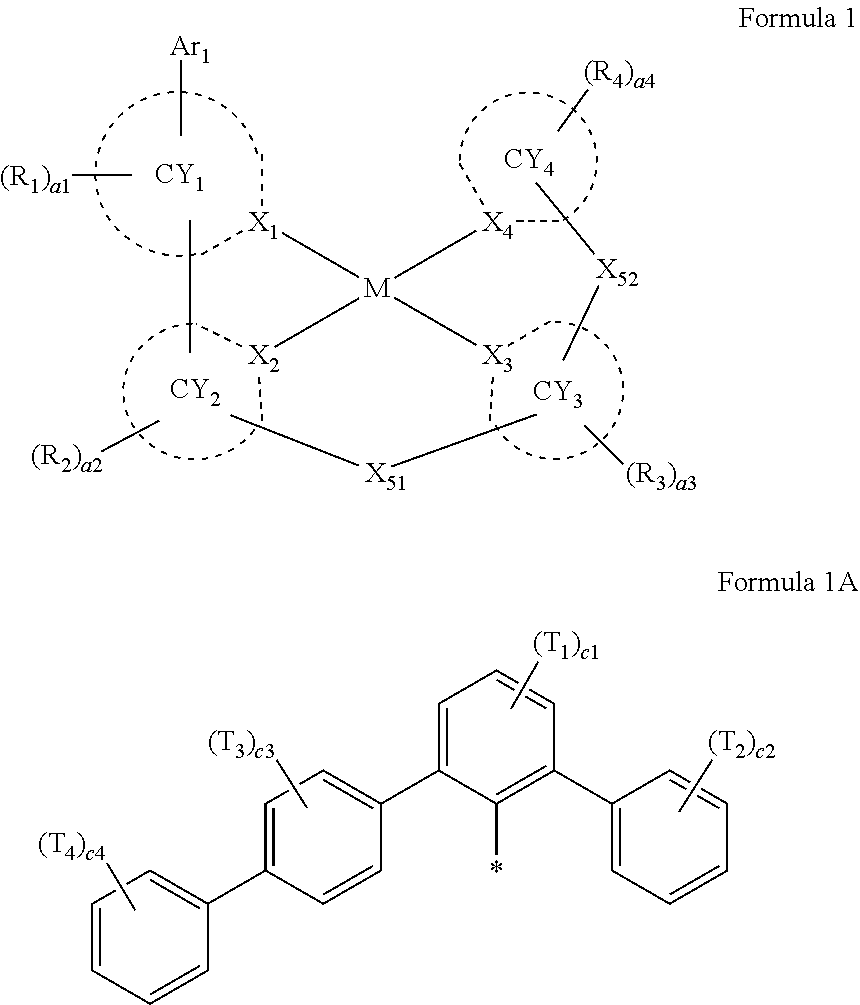
- Ar1 in Formula 1 may be a group represented by Formula 1A,
-
- * in Formula 1A indicates a binding site to ring CY1 in Formula 1,
- in Formulae 1 and 1A,
- M may be platinum (Pt), palladium (Pd), gold (Au), nickel (Ni), silver (Ag), or copper (Cu),
- X1 to X4 may each independently be C or N,
- i) a bond between X1 and M may be a coordinate bond, ii) one selected from among a bond between X2 and M, a bond between X3 and M, and a bond between X4 and M may be a coordinate bond, and two selected from among the bond between X2 and M, the bond between X3 and M, and the bond between X4 and M is each a covalent bond, (e.g., the other two bonds may each be a covalent bond), for example, each of a bond between X2 and M, a bond between X3 and M, and a bond between X4 and M may be a coordinate bond or a covalent bond, wherein one of the bonds is a coordinate bond,
- ring CY1 to ring CY4 may each independently be a C3-C60 carbocyclic group or a C1-C60 heterocyclic group,
- X51 may be a single bond, *—N(Z51a)—*′, *—B(Z51a)—*′, *—P(Z51a)—*′, *—C(Z51a)(Z51b)—*′, *—Si(Z51a)(Z51b)—*′, *—Ge(Z51a)(Z51b)—*′, *—S—*′, *—Se—*′, *—O—*′, *—C(═O)—*′, *—S(=O)—*′, *—S(═O)2—*′, *—C(Z51a)═*′, *=C(Z51a)—*′, *—C(Z51a)═C(Z51b)—*′, *—C(═S)—*′, or *—C≡C—*′,
- X52 may be a single bond, *—N(Z52a)—*′, *—B(Z52a)—*′, *—P(Z52a)—*′, *—C(Z52a)(Z52b)—*′, *—Si(Z52a)(Z52b)—*′, *—Ge(Z52a)(Z52b)—*′, *—S—*′, *—Se—*′, *—O—*′, *—C(═O)—*′, *—S(=O)—*′, *—S(═O)2—*′, *—C(Z52a)=*′, *=C(Z52a)—*′, *—C(Z52a)═C(Z52b)—*′, *—C(═S)—*′, or *—C≡C—*′,
- R1 to R4, Z51a, Z51b, Z52a, Z52b, and T1 to T4 may each independently be hydrogen, deuterium, —F, —Cl, —Br, —I, a hydroxyl group, a cyano group, a nitro group, a C1-C60 alkyl group that is unsubstituted or substituted with at least one R10a, a C2-C60 alkenyl group that is unsubstituted or substituted with at least one R10a, a C2-C60 alkynyl group that is unsubstituted or substituted with at least one R10a, a C1-C60 alkoxy group that is unsubstituted or substituted with at least one R10a, a C3-C60 carbocyclic group that is unsubstituted or substituted with at least one R10a, a C1-C60 heterocyclic group that is unsubstituted or substituted with at least one R10a, a C6-C60 aryloxy group that is unsubstituted or substituted with at least one R10a, a C6-C60 arylthio group that is unsubstituted or substituted with at least one R10a, a C7-C60 arylalkyl group that is unsubstituted or substituted with at least one R10a, a C2-C60 heteroarylalkyl group that is unsubstituted or substituted with at least one R10a, —C(Q1)(Q2)(Q3), —Si(Q1)(Q2)(Q3), —N(Q1)(Q2), —B(Q1)(Q2), —C(═O)(Q1), —S(═O)2(Q1), or —P(═O)(Q1)(Q2),
- a1 to a4 may each independently be an integer from 0 to 10,
- c1 may be an integer from 1 to 3,
- c2 and c4 may each independently be an integer from 1 to 5,
- c3 may be an integer from 1 to 4,
- in Formula 1A, a group represented by
-
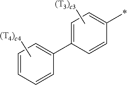
- and a group represented by
-

- may be different from each other,
-
- two or more selected from among R1, R2, R3, R4, Z51a, Z51b, Z52a, Z52b, T1, T2, T3, and T4 may optionally be bonded together to form a C3-C60 carbocyclic group that is unsubstituted or substituted with at least one R10a or a C1-C60 heterocyclic group that is unsubstituted or substituted with at least one R10a,
- * and *′ each indicate a binding site to a neighboring atom,
- R10a may be:
- deuterium, —F, —Cl, —Br, —I, a hydroxyl group, a cyano group, or a nitro group,
- a C1-C60 alkyl group, a C2-C60 alkenyl group, a C2-C60 alkynyl group, or a C1-C60 alkoxy group, each unsubstituted or substituted with deuterium, —F, —Cl, —Br, —I, a hydroxyl group, a cyano group, a nitro group, a C3-C60 carbocyclic group, a C1-C60 heterocyclic group, a C6-C60 aryloxy group, a C6-C60 arylthio group, a C7-C60 arylalkyl group, a C2-C60 heteroarylalkyl group, —Si(Q11)(Q12)(Q13), —N(Q11)(Q12), —B(Q11)(Q12), —C(═O)(Q11), —S(═O)2(Q11), —P(═O)(Q11)(Q12), or a (e.g., any) combination thereof,
- a C3-C60 carbocyclic group, a C1-C60 heterocyclic group, a C6-C60 aryloxy group, a C6-C60 arylthio group, a C7-C60 arylalkyl group, or a C2-C60 heteroarylalkyl group, each unsubstituted or substituted with deuterium, —F, —Cl, —Br, —I, a hydroxyl group, a cyano group, a nitro group, a C1-C60 alkyl group, a C2-C60 alkenyl group, a C2-C60 alkynyl group, a C1-C60 alkoxy group, a C3-C60 carbocyclic group, a C1-C60 heterocyclic group, a C6-C60 aryloxy group, a C6-C60 arylthio group, a C7-C60 arylalkyl group, a C2-C60 heteroarylalkyl group, —Si(Q21)(Q22)(Q23), —N(Q21)(Q22), —B(Q21)(Q22), —C(═O)(Q21), —S(═O)2(Q21), —P(═O)(Q21)(Q22), or a (e.g., any) combination thereof, or
- —Si(Q31)(Q32)(Q33), —N(Q31)(Q32), —B(Q31)(Q32), —C(═O)(Q31), —S(═O)2(Q31), or —P(═O)(Q31)(Q32), and
- Q1 to Q3, Q11 to Q13, Q21 to Q23, and Q31 to Q33 may each independently be: hydrogen; deuterium; —F; —Cl; —Br; —I; a hydroxyl group; a cyano group; a nitro group; or a C1-C60 alkyl group, a C2-C60 alkenyl group, a C2-C60 alkynyl group, a C1-C60 alkoxy group, a C3-C60 carbocyclic group, or a C1-C60 heterocyclic group, each unsubstituted or substituted with deuterium, —F, a cyano group, a C1-C60 alkyl group, a C1-C60 alkoxy group, a phenyl group, a biphenyl group, or a (e.g., any) combination thereof.
-
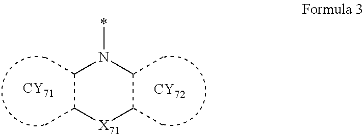
- In Formula 3,
-
- ring CY71 and ring CY72 may each independently be a π electron-rich C3-C60 cyclic group or a pyridine group,
- X71 may be a single bond, or a linking group including O, S, N, B, C, Si, or a (e.g., any) combination thereof, and
- * in Formula 3 indicates a binding site to an atom in the third compound that is not included in Formula 3 (e.g., a (e.g., any) atom included in remaining moieties other than Formula 3 in the third compound).
- According to one or more embodiments,
-
- a light-emitting device includes a first electrode,
- a second electrode facing the first electrode,
- an interlayer arranged between the first electrode and the second electrode and including an emission layer, and
- the organometallic compound represented by Formula 1.
- According to one or more embodiments, an electronic apparatus includes the light-emitting device.
- According to one or more embodiments, electronic equipment includes the light-emitting device.
- According to one or more embodiments, provided is the organometallic compound represented by Formula 1.
- The accompanying drawings are included to provide a further understanding of the preceding and other aspects, features, and advantages of certain embodiments of the disclosure are incorporated in and constitute a part of this specification. The drawings illustrate example embodiments and, together with the following description taken in conjunction with the accompanying drawings, serve to make the principles of the present disclosure more apparent. In the drawings:
-
FIG. 1 is a schematic view of a structure of a light-emitting device according to one or more embodiments of the present disclosure; -
FIGS. 2 and 3 are each a schematic view of a structure of a light-emitting apparatus which is one of electronic apparatuses, according to one or more embodiments of the present disclosure; and -
FIG. 4 is a schematic perspective view of electronic equipment including a light-emitting device according to one or more embodiments of the present disclosure; -
FIG. 5 is a schematic perspective view of the exterior of a vehicle as electronic equipment including a light-emitting device according to one or more embodiments of the present disclosure; and -
FIGS. 6A-6C are each a schematic view of the interior of a vehicle that includes electronic equipment including a light-emitting device according to one or more embodiments of the present disclosure. - Reference will now be made in more detail to embodiments, examples of which are illustrated in the accompanying drawings, wherein like reference numerals refer to like elements throughout, and duplicative descriptions thereof may not be provided the specification. In this regard, the present embodiments may have different forms and should not be construed as being limited to the descriptions set forth herein. Accordingly, the embodiments are merely described, by referring to the drawings, to explain aspects of the present description. As utilized herein, the term “and/or” includes any and all combinations of one or more of the associated listed items. Expressions such as “at least one of,” “one of,” and “selected from,” when preceding a list of elements, modify the entire list of elements and do not modify the individual elements of the list. For example, throughout the disclosure, the expression “at least one of a, b or c” indicates only a, only b, only c, both (e.g., simultaneously) a and b, both (e.g., simultaneously) a and c, both (e.g., simultaneously) b and c, all of a, b, and c, or variations thereof.
- Unless otherwise defined, all chemical names, technical and scientific terms, and terms defined in common dictionaries should be interpreted as having meanings consistent with the context of the related art, and should not be interpreted in an ideal or overly formal sense. It will be understood that, although the terms first, second, etc. may be used herein to describe various elements, these elements should not be limited by these terms. These terms are only used to distinguish one element from another element. Thus, a first element could be termed a second element without departing from the teachings of the present disclosure. Similarly, a second element could be termed a first element.
- As used herein, singular forms such as “a,” “an,” and “the” are intended to include the plural forms as well, unless the context clearly indicates otherwise.
- It will be further understood that the terms “comprise,” “comprises,” “comprising,” “has,” “have,” “having,” “include,” “includes,” and/or “including,” when used in this specification, specify the presence of stated features, steps, operations, elements, and/or components, but do not preclude the presence or addition of one or more other features, steps, operations, elements, components, and/or groups thereof.
- As used herein, the terms “use,” “using,” and “used” may be considered synonymous with the terms “utilize,” “utilizing,” and “utilized,” respectively.
- As used herein, the term “and/or” includes any, and all, combination(s) of one or more of the associated listed items.
- The term “may” will be understood to refer to “one or more embodiments of the present disclosure,” some of which include the described element and some of which exclude that element and/or include an alternate element. Similarly, alternative language such as “or” refers to “one or more embodiments of the present disclosure,” each including a corresponding listed item.
- It will be understood that when an element is referred to as being “on,” “connected to,” or “on” another element, it may be directly on, connected, or coupled to the other element or one or more intervening elements may also be present. When an element is referred to as being “directly on,” “directly connected to,” or “directly coupled to” another element, there are no intervening elements present.
- Spatially relative terms, such as “beneath,” “below,” “lower,” “above,” “upper,” “bottom,” “top,” and the like, may be used herein for ease of description to describe one element or feature's relationship to another element(s) or feature(s) as illustrated in the drawings. It will be understood that the spatially relative terms are intended to encompass different orientations of the device in use or operation in addition to the orientation depicted in the drawings. For example, if the device in the drawings is turned over, elements described as “below” or “beneath” other elements or features would then be oriented “above” or “over” the other elements or features. Thus, the term “below” may encompass both an orientation of above and below. The device may be otherwise oriented (rotated 90 degrees or at other orientations), and the spatially relative descriptors used herein should be interpreted accordingly.
- In this context, “consisting essentially of” means that any additional components will not materially affect the chemical, physical, optical or electrical properties of the semiconductor film.
- In present disclosure, “not include (or not including) a or any ‘component’”, “exclude (or excluding) a or any ‘component’”, “‘component’-free”, and/or the like refers to that the “component” not being added, selected or utilized as a component in the element/composition, but the “component” of less than a suitable amount may still be included due to other impurities and/or external factors.
- Further, in this specification, the phrase “on a plane,” or “plan view,” means viewing a target portion from the top, and the phrase “on a cross-section” means viewing a cross-section formed by vertically cutting a target portion from the side.
- According to one or more embodiments,
-
- a composition includes: an organometallic compound represented by Formula 1; and
- a second compound including at least one π electron-deficient nitrogen-containing C1-C60 heterocyclic group, a third compound including a group represented by
Formula 3, a fourth compound capable of emitting delayed fluorescence, or a (e.g., any) combination thereof, - wherein the organometallic compound, the second compound, the third compound, and the fourth compound may be different from each other:
-
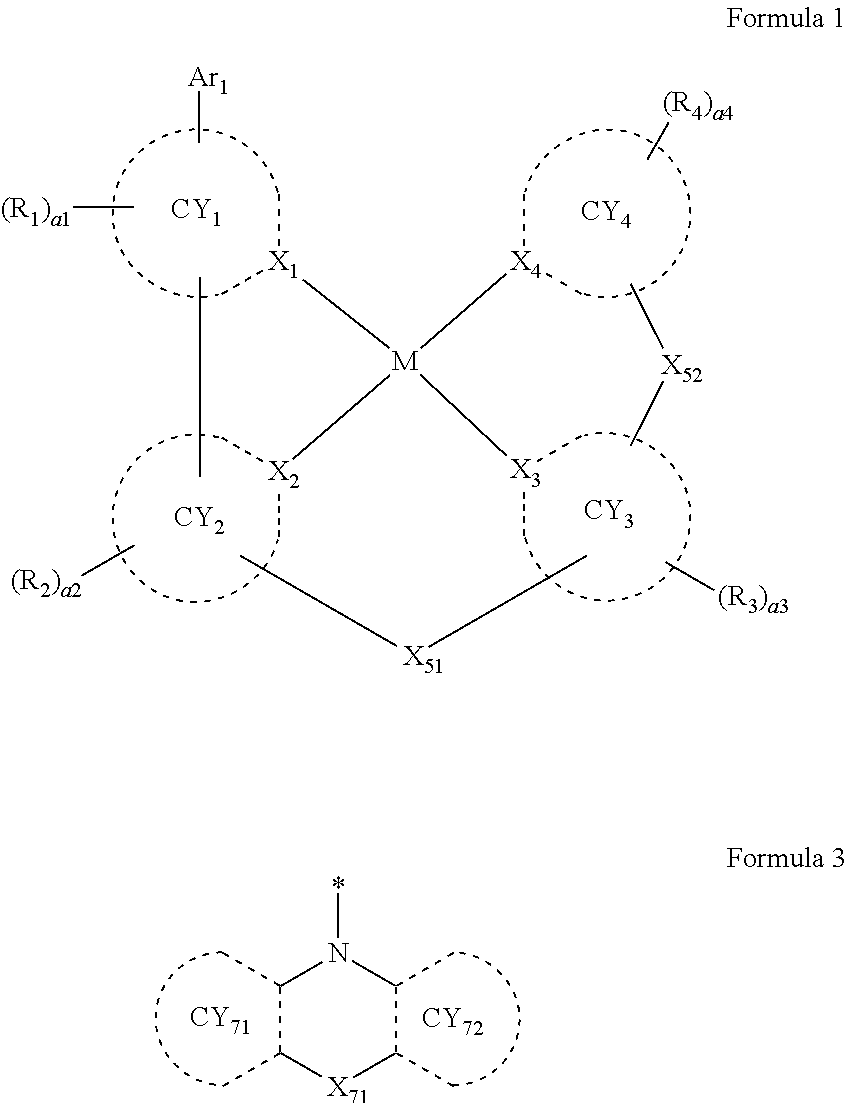
-
- wherein, in
Formula 3, - ring CY71 and ring CY72 may each independently be a π electron-rich C3-C60 cyclic group or a pyridine group,
- X71 may be a single bond, or a linking group including O, S, N, B, C, Si, or any combination thereof, and
- * in
Formula 3 indicates a binding site to an atom in the third compound that is not included in Formula 3 (e.g., a (e.g., any) atom included in remaining moieties other thanFormula 3 in the third compound).
- wherein, in
- The organometallic compound represented by Formula 1 as utilized herein may be referred to as a “first compound.”
- Formula 1 and
Formula 3 are each as described herein. - In one or more embodiments, the composition may be included in a layer. The “layer including the composition” may include a mixture including 1) the organometallic compound and 2) the second compound, the third compound, the fourth compound, or any combination thereof. Therefore, the “layer including the composition” is clearly distinguished from, for example, a double layer including 1) a first layer including the organometallic compound and 2) a second layer including the second compound, the third compound, the fourth compound, or any combination thereof.
- In one or more embodiments, the composition may be a composition prepared to form a layer including 1) the organometallic compound and 2) the second compound, the third compound, the fourth compound, or any combination thereof by utilizing one or more suitable methods such as a deposition method, a wet process, and/or the like. In one or more embodiments, the composition may be a pre-mixed mixture prepared for utilizing in a deposition method (for example, a vacuum deposition method). The pre-mixed mixture may be charged, for example, into a deposition source within a vacuum chamber, and two or more compounds included in the pre-mixed mixture may be co-deposited.
- In one or more embodiments, a weight ratio of the organometallic compound and the second compound in the composition may be 10:90 to 90:10 or 20:80 to 80:20.
- According to one or more embodiments, a light-emitting device includes: a first electrode;
-
- a second electrode facing the first electrode;
- an interlayer arranged between the first electrode and the second electrode and including an emission layer; and
- the organometallic compound represented by Formula 1.
- Formula 1 is as described herein.
- The light-emitting device includes the organometallic compound represented by Formula 1, and thus, may have improved color purity, improved luminescence efficiency, and improved lifespan characteristics.
- In one or more embodiments, the interlayer in the light-emitting device may include the organometallic compound.
- In one or more embodiments, the emission layer in the light-emitting device may include the organometallic compound.
- In one or more embodiments, the light-emitting device may further include a second compound including at least one π electron-deficient nitrogen-containing C1-C60 heterocyclic group, a third compound including a group represented by
Formula 3, a fourth compound capable of emitting delayed fluorescence, or a (e.g., any) combination thereof, and -
- the organometallic compound, the second compound, the third compound, and the fourth compound in the light-emitting device may be different from each other.
- The second compound to the fourth compound in the composition and the light-emitting device are each as described herein.
- In one or more embodiments, the organometallic compound may include at least one deuterium.
- In one or more embodiments, the second compound to the fourth compound may each include at least one deuterium.
- In one or more embodiments, the second compound may include at least one silicon.
- In one or more embodiments, the third compound may include at least one silicon.
- In one or more embodiments, the composition and the light-emitting device (for example, the emission layer in the light-emitting device) may each further include a second compound and a third compound, in addition to the organometallic compound represented by Formula 1, and at least one of the second compound and the third compound may include at least one deuterium, at least one silicon, or a combination thereof.
- In one or more embodiments, the composition and the light-emitting device (for example, the emission layer in the light-emitting device) may each further include a second compound, in addition to the organometallic compound. At least one of the organometallic compound and the second compound may include at least one deuterium. In one or more embodiments, each of the composition and the light-emitting device (for example, the emission layer in the light-emitting device) may further include a third compound, a fourth compound, or any combination thereof, in addition to the organometallic compound and the second compound.
- In one or more embodiments, the composition and the light-emitting device (for example, the emission layer in the light-emitting device) may each further include a third compound, in addition to the organometallic compound. At least one of the organometallic compound and the third compound may include at least one deuterium. In one or more embodiments, each of the composition and the light-emitting device (for example, the emission layer in the light-emitting device) may further include a second compound, a fourth compound, or any combination thereof, in addition to the organometallic compound and the third compound.
- In one or more embodiments, the composition and the light-emitting device (for example, the emission layer in the light-emitting device) may each further include a fourth compound, in addition to the organometallic compound. At least one of the organometallic compound and the fourth compound may include at least one deuterium. The fourth compound may serve to improve color purity, luminescence efficiency, and lifespan characteristics of the light-emitting device. In one or more embodiments, each of the composition and the light-emitting device (for example, the emission layer in the light-emitting device) may further include a second compound, a third compound, or any combination thereof, in addition to the organometallic compound and the fourth compound.
- In one or more embodiments, the composition and the light-emitting device (for example, the emission layer in the light-emitting device) may each further include a second compound and a third compound, in addition to the organometallic compound. The second compound and the third compound may form an exciplex. At least one of the organometallic compound, the second compound, and the third compound may include at least one deuterium.
- In one or more embodiments, a highest occupied molecular orbital (HOMO) energy level of the organometallic compound may be about −5.35 electron volt (eV) to about −5.15 eV or about −5.30 eV to about −5.20 eV.
- In one or more embodiments, a lowest unoccupied molecular orbital (LUMO) energy level of the organometallic compound may be about −2.20 eV to about −1.80 eV or about −2.15 eV to about −1.90 eV.
- The HOMO and LUMO energy levels may be evaluated via cyclic voltammetry analysis (for example, Evaluation Example 1 as described herein) for the organometallic compound.
- In one or more embodiments, the maximum emission wavelength (or emission peak wavelength) of the photoluminescence (PL) spectrum in a film of the organometallic compound may be about 430 nanometer (nm) to about 475 nm, about 440 nm to about 475 nm, about 450 nm to about 475 nm, about 430 nm to about 470 nm, about 440 nm to about 470 nm, about 450 nm to about 470 nm, about 430 nm to about 465 nm, about 440 nm to about 465 nm, about 450 nm to about 465 nm, about 430 nm to about 460 nm, about 440 nm to about 460 nm, or about 450 nm to about 460 nm.
- In one or more embodiments, the emission full width at half maximum (FWHM) of the PL spectrum in a film of the organometallic compound may be 40 nm or less, about 5 nm to about 40 nm, about 10 nm to about 40 nm, about 15 nm to about 40 nm, about 20 nm to about 40 nm, about 5 nm to about 38 nm, about 10 nm to about 38 nm, about 15 nm to about 38 nm, or about 20 nm to about 38 nm.
- In one or more embodiments, the photoluminescence quantum yield (PLQY) in a film of the organometallic compound may be about 50% to about 99% or about 55% to about 90%.
- In one or more embodiments, the decay time of the organometallic compound may be about 1.80 microsecond (μs) to about 3.00 μs, about 1.90 μs to about 2.70 μs, or about 1.90 μs to about 2.50 μs.
- The maximum emission wavelength, emission FWHM, PLQY, and decay time of the organometallic compound were evaluated for a film including the organometallic compound, and an evaluation method thereof is as described in connection with, for example, Evaluation Examples 2 and 3 as described herein.
- In one or more embodiments, the emission layer of the light-emitting device may include: i) the organometallic compound; and ii) the second compound, the third compound, the fourth compound, or any combination thereof, and the emission layer may be to emit blue light.
- In one or more embodiments, the maximum emission wavelength of the blue light may be about 430 nm to about 475 nm, about 440 nm to about 475 nm, about 450 nm to about 475 nm, about 430 nm to about 470 nm, about 440 nm to about 470 nm, about 450 nm to about 470 nm, about 430 nm to about 465 nm, about 440 nm to about 465 nm, or about 450 nm to about 465 nm.
- In one or more embodiments, the emission FWHM of the blue light may be 40 nm or less, about 5 nm to about 40 nm, about 10 nm to about 40 nm, about 15 nm to about 40 nm, about 20 nm to about 40 nm, about 5 nm to about 38 nm, about 10 nm to about 38 nm, about 15 nm to about 38 nm, or about 20 nm to about 38 nm.
- In one or more embodiments, the blue light may be deep blue light.
- In one or more embodiments, the CIEx coordinate (for example, the bottom emission CIEx coordinate) of the blue light may be about 0.125 to about 0.140 or about 0.130 to about 0.140.
- In one or more embodiments, the CIEy coordinate (for example, the bottom emission CIEy coordinate) of the blue light may be about 0.100 to about 0.130.
- Examples of the maximum emission wavelength and CIEy coordinate of the blue light are as described herein in Tables 7 and 9.
- In one or more embodiments, the second compound may include a pyridine group, a pyrimidine group, a pyrazine group, a pyridazine group, a triazine group, or any combination thereof.
- In one or more embodiments, the following compounds may be excluded from the third compound.
-

- In one or more embodiments, a difference between the triplet energy level (eV) of the fourth compound and the singlet energy level (eV) of the fourth compound may be about 0 eV or higher and about 0.5 eV or lower (or, about 0 eV or higher and about 0.3 eV or lower).
- In one or more embodiments, the fourth compound may include at least one cyclic group including each of boron (B) and nitrogen (N) as a ring-forming atom.
- In one or more embodiments, the fourth compound may be a C8-C60 polycyclic group-containing compound including at least two condensed cyclic groups that share boron (B).
- In one or more embodiments, the fourth compound may include a condensed ring in which at least one third ring and at least one fourth ring are condensed together,
-
- the third ring may be a cyclopentane group, a cyclohexane group, a cycloheptane group, a cyclooctane group, a cyclopentene group, a cyclohexene group, a cycloheptene group, a cyclooctene group, an adamantane group, a norbornene group, a norbornane group, a bicyclo[1.1.1]pentane group, a bicyclo[2.1.1]hexane group, a bicyclo[2.2.2]octane group, a benzene group, a pyridine group, a pyrimidine group, a pyridazine group, a pyrazine group, or a triazine group, and
- the fourth ring may be a 1,2-azaborinine group, a 1,3-azaborinine group, a 1,4-azaborinine group, a 1,2-dihydro-1,2-azaborinine group, a 1,4-oxaborinine group, a 1,4-thiaborinine group, or a 1,4-dihydroborinine group.
- In one or more embodiments, the third compound may not include (e.g., may exclude) a compound represented by Formula 3-1 described herein.
- In one or more embodiments, the second compound may include a compound represented by Formula 2:
-
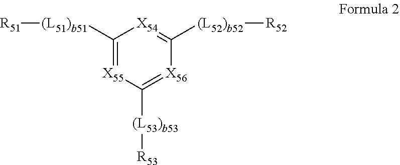
-
- wherein, in
Formula 2,
- wherein, in
- L51 to L53 may each independently be a single bond, a C3-C60 carbocyclic group that is unsubstituted or substituted with at least one R10a, or a C1-C60 heterocyclic group that is unsubstituted or substituted with at least one R10a,
-
- b51 to b53 may each independently be an integer from 1 to 5,
- X54 may be N or C(R54), X55 may be N or C(R55), X56 may be N or C(R5s), and at least one of X54 to X56 may be N, and
- R51 to R56 and R10a are each as described herein.
- In one or more embodiments, the third compound may include a compound represented by Formula 3-1, a compound represented by Formula 3-2, a compound represented by Formula 3-3, a compound represented by Formula 3-4, a compound represented by Formula 3-5, or any combination thereof:
-

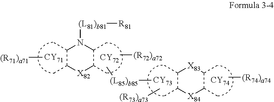
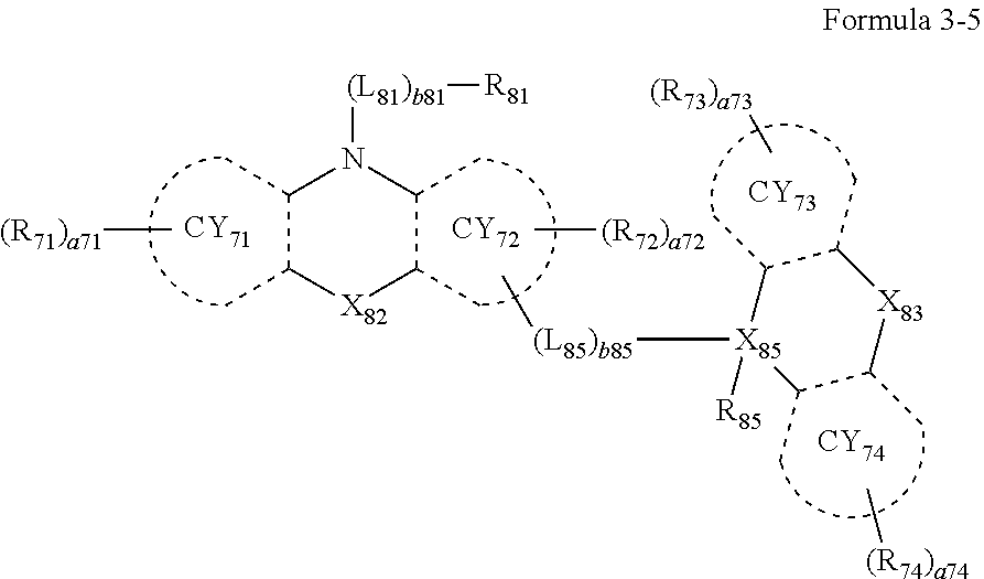
-
- wherein, in Formulae 3-1 to 3-5,
- ring CY71 to ring CY74 may each independently be a π electron-rich C3-C60 cyclic group or a pyridine group,
- X82 may be a single bond, O, S, N-[(L82)b82-R82], C(R82a)(R82b), or Si(R82a)(R82b),
- X83 may be a single bond, O, S, N-[(L83)b83-R83], C(R83a)(R83b), or Si(R83a)(R83b),
- X84 may be O, S, N-[(L84)b84-R84], C(R84a)(R84b), or Si(R84a)(R84b),
- X85 may be C or Si,
- L81 to L85 may each independently be a single bond, *—C(Q4)(Q5)-*′, *—Si(Q4)(Q5)-*′, a π electron-rich C3-C60 cyclic group that is unsubstituted or substituted with at least one R10a or a pyridine group that is unsubstituted or substituted with at least one R10a, wherein Q4 and Q5 are each as described in connection with Q1,
- b81 to b85 may each independently be an integer from 1 to 5,
- R71 to R74, R81 to R85, R82a, R82b, R83a, R83b, R84a, and R84b are each as described herein,
- a71 to a74 may each independently be an integer from 0 to 20, and
- R10a is as described herein.
- In one or more embodiments, the fourth compound may include a compound represented by Formula 502, a compound represented by Formula 503, or a (e.g., any) combination thereof:
-

-
- wherein, in Formulae 502 and 503,
- ring A501 to ring A504 may each independently be a C3-C60 carbocyclic group or a C1-C60 heterocyclic group,
- Y505 may be O, S, N(R505), B(R505), C(R505a)(R505b), or Si(R505a)(R505b),
- Y506 may be O, S, N(R506), B(R506), C(R506a)(R506b), or Si(R506a)(R506b),
- Y507 may be O, S, N(R507), B(R507), C(R507a)(R507b), or Si(R507a)(R507b),
- Y508 may be O, S, N(R508), B(R508), C(R508a)(R508b), or Si(R508a)(R58b),
- Y51 and Y52 may each independently be B, P(═O), or S(═O),
- R500a, R500b, R501 to R508, R505a, R505b, R506a, R506b, R507a, R507b, R508a, and R508b are each as described herein, and
- a501 to a504 may each independently be an integer from 0 to 20.
- In one or more embodiments, the light-emitting device may satisfy at least one of (e.g., at least one selected from among) Conditions 1 to 4:
- LUMO energy level (eV) of third compound>LUMO energy level (eV) of organometallic compound;
- LUMO energy level (eV) of organometallic compound>LUMO energy level (eV) of second compound;
- HOMO energy level (eV) of organometallic compound>HOMO energy level (eV) of third compound; and
- HOMO energy level (eV) of third compound>HOMO energy level (eV) of second compound.
- Each of the HOMO energy level and the LUMO energy level of each of the organometallic compound, the second compound, and the third compound may be a negative value, and may be measured according to a suitable method, for example, a method described in Evaluation Example 1.
- In one or more embodiments, an absolute value of a difference between a LUMO energy level of the organometallic compound and a LUMO energy level of the second compound may be about 0.1 eV or higher and about 1.0 eV or lower, an absolute value of a difference between a LUMO energy level of the organometallic compound and a LUMO energy level of the third compound may be about 0.1 eV or higher and about 1.0 eV or lower, an absolute value of a difference between a HOMO energy level of the organometallic compound and a HOMO energy level of the second compound may be about 1.25 eV or lower (for example, about 1.25 eV or lower and about 0.2 eV or higher), and an absolute value of a difference between a HOMO energy level of the organometallic compound and a HOMO energy level of the third compound may be about 1.25 eV or lower (for example, about 1.25 eV or lower and about 0.2 eV or higher).
- When the relationships between LUMO energy level and HOMO energy level satisfy the conditions as described herein, the balance between holes and electrons injected into the emission layer may be achieved.
- The light-emitting device may have a structure of a first embodiment or a second embodiment.
- According to the first embodiment, the organometallic compound may be included in the emission layer in the interlayer of the light-emitting device, wherein the emission layer may further include a host, the organometallic compound and the host may be different from each other, and the emission layer may be to emit phosphorescence or fluorescence emitted from the organometallic compound. In other words, according to the first embodiment, the organometallic compound may be a dopant or an emitter. In one or more embodiments, the organometallic compound may be a phosphorescent dopant or a phosphorescent emitter.
- Phosphorescence or fluorescence emitted from the organometallic compound may be blue light.
- The emission layer may further include an auxiliary dopant. The auxiliary dopant may serve to improve luminescence efficiency from the organometallic compound by effectively transferring a dopant or the organometallic compound as an emitter.
- The auxiliary dopant may be different from each of the organometallic compound and the host.
- In one or more embodiments, the auxiliary dopant may be a delayed fluorescence-emitting compound.
- In one or more embodiments, the auxiliary dopant may be a compound including at least one cyclic group including each of boron (B) and nitrogen (N) as a ring-forming atom.
- According to the second embodiment, the organometallic compound may be included in the emission layer in the interlayer of the light-emitting device, wherein the emission layer may further include a host and a dopant, the organometallic compound, the host and the dopant may be different from one another, and the emission layer may be to emit phosphorescence or fluorescence (for example, delayed fluorescence) from the dopant.
- In one or more embodiments, the organometallic compound in the second embodiment may serve as an auxiliary dopant that transfers energy to a dopant (or an emitter), not as a dopant.
- In one or more embodiments, the organometallic compound in the second embodiment may serve as an emitter and as an auxiliary dopant that transfers energy to a dopant (or an emitter).
- For example, phosphorescence or fluorescence emitted from the dopant (or the emitter) in the second embodiment may be blue phosphorescence or blue fluorescence (e.g., blue delayed fluorescence).
- The dopant (or the emitter) in the second embodiment may be a phosphorescent dopant material (for example, the organometallic compound represented by Formula 1, the organometallic compound represented by Formula 401, or any combination thereof) or any fluorescent dopant material (for example, the compound represented by Formula 501, the compound represented by Formula 502, the compound represented by Formula 503, or any combination thereof).
- In the first embodiment and the second embodiment, the blue light may be blue light having a maximum emission wavelength of about 390 nm to about 500 nm, about 410 nm to about 490 nm, about 430 nm to about 480 nm, about 440 nm to about 475 nm, or about 455 nm to about 470 nm.
- The auxiliary dopant in the first embodiment may include, for example, the fourth compound represented by Formula 502 or Formula 503.
- The host in the first embodiment and the second embodiment may be any host material (for example, a compound represented by Formula 301, a compound represented by 301-1, a compound represented by Formula 301-2, or any combination thereof).
- In one or more embodiments, the host in the first embodiment and the second embodiment may be the second compound, the third compound, or any combination thereof.
- In one or more embodiments, the light-emitting device may further include a capping layer located outside the first electrode and/or outside the second electrode.
- In one or more embodiments, the light-emitting device may further include at least one of a first capping layer located outside the first electrode and a second capping layer located outside the second electrode, and at least one of the first capping layer and the second capping layer may include the organometallic compound represented by Formula 1. The first capping layer and/or the second capping layer are each as described herein.
- In one or more embodiments, the light-emitting device may further include:
-
- a first capping layer located outside the first electrode and including the organometallic compound represented by Formula 1;
- a second capping layer located outside the second electrode and including the organometallic compound represented by Formula 1; or
- the first capping layer and the second capping layer.
- The expression “(interlayer and/or a capping layer) includes an organometallic compound represented by Formula 1” as utilized herein may be to refer to that the (interlayer and/or the capping layer) may include one kind of organometallic compound represented by Formula 1 or two or more different kinds of organometallic compounds, each represented by Formula 1.
- In one or more embodiments, the interlayer and/or the capping layer may include Compound 1 only as the organometallic compound. In this regard, Compound 1 may be present in the emission layer of the light-emitting device. In one or more embodiments, the interlayer may include, as the organometallic compound, Compound 1 and
Compound 2. In this regard, Compound 1 andCompound 2 may be present in substantially the same layer (for example, all of Compound 1 andCompound 2 may be present in the emission layer), or may be present in different layers (for example, Compound 1 may be present in the emission layer, andCompound 2 may be present in the electron transport region). - The term “interlayer” as utilized herein refers to a single layer and/or all of a plurality of layers arranged between the first electrode and the second electrode of the light-emitting device.
- According to one or more embodiments, an electronic apparatus includes the light-emitting device. The electronic apparatus may further include a thin-film transistor. For example, the electronic apparatus may further include a thin-film transistor including a source electrode and a drain electrode, and the first electrode of the light-emitting device may be electrically connected to the source electrode or the drain electrode. In one or more embodiments, the electronic apparatus may further include a color filter, a color conversion layer, a touch screen layer, a polarizing layer, or any combination thereof. More details of the electronic apparatus may be referred to the descriptions provided herein.
- According to one or more embodiments, electronic equipment includes the light-emitting device.
- For example, the electronic equipment may be at least one selected from among a flat panel display, a curved display, a computer monitor, a medical monitor, a television, a billboard, an indoor or outdoor light and/or light for signal, a head-up display, a fully or partially transparent display, a flexible display, a rollable display, a foldable display, a stretchable display, a laser printer, a telephone, a portable phone, a tablet personal computer, a phablet, a personal digital assistant (PDA), a wearable device, a laptop computer, a digital camera, a camcorder, a viewfinder, a micro display, a three-dimensional (3D) display, a virtual reality or augmented reality display, a vehicle, a video wall with multiple displays tiled together, a theater or stadium screen, a phototherapy device, and a signboard, or a combination thereof.
- According to one or more embodiments, provided is the organometallic compound represented by Formula 1. Formula 1 is as described herein.
- Methods of synthesizing the organometallic compound may be easily understood by those of ordinary skill in the art by referring to Synthesis Examples and/or Examples described herein.
- Ar1 in Formula 1 may be a group represented by Formula 1A:
-

-
- wherein * in Formula 1A indicates a binding site to ring CY1 in Formula 1.
- Description of Formula 1A (or description of Ar1 in Formula 1) is as provided herein.
- In Formula 1, M may be platinum (Pt), palladium (Pd), gold (Au), nickel (Ni), silver (Ag), or copper (Cu).
- In one or more embodiments, M may be Pt.
- In Formula 1, X1 to X4 may each independently be C or N.
- In one or more embodiments, X1 may be C. In one or more embodiments, X1 in Formula 1 may be C, and C may be carbon of a carbene moiety.
- In one or more embodiments, X1 in Formula 1 may be N.
- In one or more embodiments, X2 and X3 may each be C, and X4 may be N.
- In Formula 1, i) a bond between X1 and M may be a coordinate bond, ii) one selected from among a bond between X2 and M, a bond between X3 and M, and a bond between X4 and M may be a coordinate bond, and two selected from among the bond between X2 and M, the bond between X3 and M, and the bond between X4 and M is each a covalent bond, (e.g., the other two may each be a covalent bond. For example, each of a bond between X2 and M, a bond between X3 and M, and a bond between X4 and M may be a coordinate bond or a covalent bond, wherein one of the bonds is a coordinate bond.
- In one or more embodiments, a bond between X2 and M and a bond between X3 and M may each be a covalent bond, and a bond between X4 and M may be a coordinate bond.
- In one or more embodiments, X4 may be N, and a bond between X4 and M may be a coordinate bond.
- In Formula 1, ring CY1 to ring CY4 may each independently be a C3-C60 carbocyclic group or a C1-C60 heterocyclic group.
- For example, ring CY1 may be a nitrogen-containing C1-C60 heterocyclic group.
- Ring CY1 in Formula 1 may be i) an X1-containing 5-membered ring, ii) an X1-containing 5-membered ring in which at least one 6-membered ring is condensed, or iii) an X1-containing 6-membered ring.
- In one or more embodiments, ring CY1 in Formula 1 may be i) an X1-containing 5-membered ring or ii) an X1-containing 5-membered ring in which at least one 6-membered ring is condensed. For example, ring CY1 may include a 5-membered ring bonded to M in Formula 1 via X1. Here, the X1-containing 5-membered ring may be a pyrrole group, a pyrazole group, an imidazole group, a triazole group, an oxazole group, an isoxazole group, a thiazole group, an isothiazole group, an oxadiazole group, or a thiadiazole group, and the X1-containing 6-membered ring and the 6-membered ring which may be optionally condensed to the X1-containing 5-membered ring may each independently be a benzene group, a pyridine group, or a pyrimidine group.
- In one or more embodiments, ring CY1 may be an X1-containing 5-membered ring, and the X1-containing 5-membered ring may be an imidazole group or a triazole group.
- In one or more embodiments, ring CY1 may be an X1-containing 5-membered ring in which at least one 6-membered ring is condensed, and the X1-containing 5-membered ring in which the at least one 6-membered ring is condensed may be a benzimidazole group or an imidazopyridine group.
- In one or more embodiments, ring CY1 may be an imidazole group, a triazole group, a benzimidazole group, a naphthoimidazol group, or an imidazopyridine group.
- In one or more embodiments, X1 may be C, and ring CY1 may be an imidazole group, a triazole group, a benzimidazole group, a naphthoimidazol group, or an imidazopyridine group.
- In one or more embodiments, ring CY2, ring CY3, and ring CY4 may each independently be a benzene group, a pyridine group, a pyrimidine group, a pyrazine group, a pyridazine group, a triazine group, a naphthalene group, a quinoline group, an isoquinoline group, a dibenzofuran group, a dibenzothiophene group, a carbazole group, a fluorene group, a dibenzosilole group, a naphthobenzofuran group, a naphthobenzothiophene group, a benzocarbazole group, a benzofluorene group, a naphthobenzosilole group, a dinaphthofuran group, a dinaphthothiophene group, a dibenzocarbazole group, a dibenzofluorene group, a dinaphthosilole group, an azadibenzofuran group, an azadibenzothiophene group, an azacarbazole group, an azafluorene group, an azadibenzosilole group, an azanaphthobenzofuran group, an azanaphthobenzothiophene group, an azabenzocarbazole group, an azabenzofluorene group, an azanaphthobenzosilole group, an azadinaphthofuran group, an azadinaphthothiophene group, an azadibenzocarbazole group, an azadibenzofluorene group, or an azadinaphthosilole group.
- In one or more embodiments, ring CY2 may be a benzene group, a pyridine group, a pyrimidine group, a naphthalene group, a dibenzofuran group, a dibenzothiophene group, a carbazole group, a fluorene group, or a dibenzosilole group.
- In one or more embodiments, ring CY3 may be a benzene group, a naphthalene group, a dibenzofuran group, a dibenzothiophene group, a carbazole group, a fluorene group, a dibenzosilole group, a naphthobenzofuran group, a naphthobenzothiophene group, a benzocarbazole group, a benzofluorene group, a naphthobenzosilole group, a dinaphthofuran group, a dinaphthothiophene group, a dibenzocarbazole group, a dibenzofluorene group, a dinaphthosilole group, an azadibenzofuran group, an azadibenzothiophene group, an azacarbazole group, an azafluorene group, an azadibenzosilole group, an azanaphthobenzofuran group, an azanaphthobenzothiophene group, an azabenzocarbazole group, an azabenzofluorene group, an azanaphthobenzosilole group, an azadinaphthofuran group, an azadinaphthothiophene group, an azadibenzocarbazole group, an azadibenzofluorene group, or an azadinaphthosilole group.
- In one or more embodiments, ring CY3 may be a carbazole group, a benzocarbazole group, a dibenzocarbazole group, an azacarbazole group, an azabenzocarbazole group, or an azadibenzocarbazole group.
- In one or more embodiments, ring CY4 may be a pyridine group, a pyrimidine group, a pyrazine group, a pyridazine group, a triazine group, a quinoline group, or an isoquinoline group.
- X51 in Formula 1 may be a single bond, *—N(Z51a)—*′, *—B(Z51a)—*′, *—P(Z51a)—*′, *—C(Z51a)(Z51b)—*′, *—Si(Z51a)(Z51b)—*′, *—Ge(Z51a)(Z51b)—*′, *—S—*′, *—Se—*′, *—O—*′, *—C(═O)—*′, *—S(═O)—*′, *—S(═O)2—*′, *—C(Z51a)=*′, *=C(Z51a)—*′, *—C(Z51a)═C(Z51b)—*′, *—C(═S)—*′, or *—C≡C—*′. Z51a and Z51b are each as described herein. Z51a and Z51b may optionally be bonded together to form a C3-C60 carbocyclic group that is unsubstituted or substituted with at least one R10a or a C1-C60 heterocyclic group that is unsubstituted or substituted with at least one R10a.
- For example, X51 may be *—N(Z51a)—*′, *—B(Z51a)—*′, *—P(Z51a)—*′, *—C(Z51a)(Z51b)—*′, *—Si(Z51a)(Z51b)—*′, *—Ge(Z51a)(Z51b)—*′, *—S—*′, *—Se—*′, or *—O—*′.
- X52 in Formula 1 may be a single bond, *—N(Z52a)—*′, *—B(Z52a)—*′, *—P(Z52a)—*′, *—C(Z52a)(Z52b)—*′, *—Si(Z52a)(Z52b)—*′, *—Ge(Z52a)(Z52b)—*′, *—S—*′, *—Se—*′, *—O—*′, *—C(═O)—*′, *—S(═O)—*′, *—S(═O)2—*′, *—C(Z52a)=*′, *=C(Z52a)—*′, *—C(Z52a)═C(Z52b)—*′, *—C(═S)—*′, or *—C≡C—*′. Z52a and Z52b are each as described herein. Z52a and Z52b may optionally be bonded together to form a C3-C60 carbocyclic group that is unsubstituted or substituted with at least one R10a or a C1-C60 heterocyclic group that is unsubstituted or substituted with at least one R10a.
- X52 in Formula 1 may be a single bond, *—N(Z52a)—*′, *—B(Z52a)—*′, *—P(Z52a)—*′, *—C(Z52a)(Z52b)—*′, *—Si(Z52a)(Z52b)—*′, *—Ge(Z52a)(Z52b)—*′, *—S—*′, *—Se—*′, or *—O—*′. * and each indicate a binding site to a neighboring atom.
- In one or more embodiments, in Formula 1,
-
- i) X52 may be a single bond, and a group represented by
-
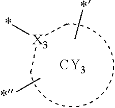
-
- in Formula 1 may be a group represented by Formula CY3A or CY3B,
- ii) X52 may not be a single bond, and a group represented by
-

-
- in Formula 1 may be a group represented by Formula CY3C, or
- iii) X52 may be *—N(R52a)—*′, and R52a and R3 may be bonded together to form a C3-C60 carbocyclic group that is unsubstituted or substituted with at least one R10a or a C1-C60 heterocyclic group that is unsubstituted or substituted with at least one R10a:
-
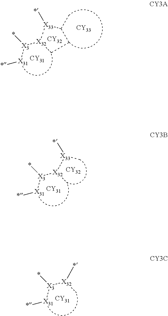
-
- wherein, in Formulae CY3A to CY3C,
- X3 and X31 to X33 may each independently be C or N,
- ring CY31, ring CY32, and ring CY33 are each a C2-C8 monocyclic group,
- a bond between X31 and X3, a bond between X3 and X32, and a bond between X32 and X33 may each be a chemical bond,
- *″ indicates a binding site to X51,
- * indicates a binding site to M in Formula 1, and
- *′ indicates a binding site to X52.
- In one or more embodiments, in Formulae CY3A and CY3B, X31, X3, and X32 may each be C, and X33 may be N.
- In one or more embodiments, X31, X3, and X32 in Formula CY3C may each be C.
- In Formulae 1 and 1A, R1 to R4, Z51a, Z51b, Z52a, Z52b, and T1 to T4 may each independently be hydrogen, deuterium, —F, —Cl, —Br, —I, a hydroxyl group, a cyano group, a nitro group, a C1-C60 alkyl group that is unsubstituted or substituted with at least one R10a, a C2-C60 alkenyl group that is unsubstituted or substituted with at least one R10a, a C2-C60 alkynyl group that is unsubstituted or substituted with at least one R10a, a C1-C60 alkoxy group that is unsubstituted or substituted with at least one R10a, a C3-C60 carbocyclic group that is unsubstituted or substituted with at least one R10a, a C1-C60 heterocyclic group that is unsubstituted or substituted with at least one R10a, a C6-C60 aryloxy group that is unsubstituted or substituted with at least one R10a, a C6-C60 arylthio group that is unsubstituted or substituted with at least one R10a, a C7-C60 arylalkyl group that is unsubstituted or substituted with at least one R10a, a C2-C60 heteroarylalkyl group that is unsubstituted or substituted with at least one R10a, —C(Q1)(Q2)(Q3), —Si(Q1)(Q2)(Q3), —N(Q1)(Q2), —B(Q1)(Q2), —C(═O)(Q1), —S(═O)2(Q1), or —P(═O)(Q1)(Q2). Q1 to Q3 are each as described herein.
- In one or more embodiments, R1 to R4, Z51a, Z51b, Z52a, Z52b, and T1 to T4 in Formulae 1 and 1A may each independently be:
-
- hydrogen, deuterium, —F, or a cyano group;
- a C1-C20 alkyl group that is unsubstituted or substituted with deuterium, —F, a cyano group, a phenyl group, a deuterated phenyl group, a fluorinated phenyl group, a (C1-C20 alkyl)phenyl group, a biphenyl group, a deuterated biphenyl group, a fluorinated biphenyl group, a (C1-C20 alkyl)biphenyl group, or a (e.g., any) combination thereof; or
- a C3-C10 cycloalkyl group, a phenyl group, a naphthyl group, a dibenzofuranyl group, or a dibenzothiophenyl group, each unsubstituted or substituted with deuterium, —F, cyano group, a C1-C20 alkyl group, a deuterated C1-C20 alkyl group, a fluorinated C1-C20 alkyl group, a phenyl group, a deuterated phenyl group, a fluorinated phenyl group, a (C1-C20 alkyl)phenyl group, a biphenyl group, a deuterated biphenyl group, a fluorinated biphenyl group, a (C1-C20 alkyl)biphenyl group, or a (e.g., any) combination thereof.
- In one or more embodiments, R4 in Formula 1 may be:
-
- hydrogen, deuterium, —F, or a cyano group; or
- a C1-C20 alkyl group that is unsubstituted or substituted with deuterium, —F, a cyano group, a phenyl group, a deuterated phenyl group, a fluorinated phenyl group, a (C1-C20 alkyl)phenyl group, a biphenyl group, a deuterated biphenyl group, a fluorinated biphenyl group, a (C1-C20 alkyl)biphenyl group, or a (e.g., any) combination thereof.
- In one or more embodiments, R4 in Formula 1 may be:
-
- hydrogen, deuterium, —F, or a cyano group; or
- a C1-C20 alkyl group that is unsubstituted or substituted with deuterium, —F, a cyano group, or a (e.g., any) combination thereof.
- In one or more embodiments, T1 to T4 in Formula 1A may each independently be:
-
- hydrogen, deuterium, —F, or a cyano group; or
- a C1-C20 alkyl group that is unsubstituted or substituted with deuterium, —F, a cyano group, or a (e.g., any) combination thereof.
- The “C1-C60 alkyl group that is unsubstituted or substituted with at least one deuterium” and the “C1-C20 alkyl group that is unsubstituted or substituted with at least one deuterium” as utilized herein may be, for example, a methyl group, an ethyl group, an n-propyl group, an iso-propyl group, an n-butyl group, a sec-butyl group, an isobutyl group, a tert-butyl group, an n-pentyl group, a tert-pentyl group, a neopentyl group, an isopentyl group, a sec-pentyl group, a 3-pentyl group, a sec-isopentyl group, an n-hexyl group, an iso-hexyl group, a sec-hexyl group, a tert-hexyl group, an n-heptyl group, an iso-heptyl group, a sec-heptyl group, a tert-heptyl group, an n-octyl group, an iso-octyl group, a sec-octyl group, a tert-octyl group, an n-nonyl group, an iso-nonyl group, a sec-nonyl group, a tert-nonyl group, an n-decyl group, an iso-decyl group, a sec-decyl group, or a tert-decyl group, each unsubstituted or substituted with at least one deuterium.
- In one or more embodiments, the “C1-C60 alkyl group that is unsubstituted or substituted with at least one deuterium” and the “C1-C20 alkyl group that is unsubstituted or substituted with at least one deuterium” may be —CH3, —CDH2, —CD2H, —CD3, —CH2CH3, —CDHCH3, —CD2CH3, —CH2CDH2, —CDHCDH2, —CD2CDH2, —CH2CD2H, —CDHCD2H, —CD2CD2H, —CH2CD3, —CDHCD3, —CD2CD3, or a group represented by one of Formulae X-1 to X-30:
-
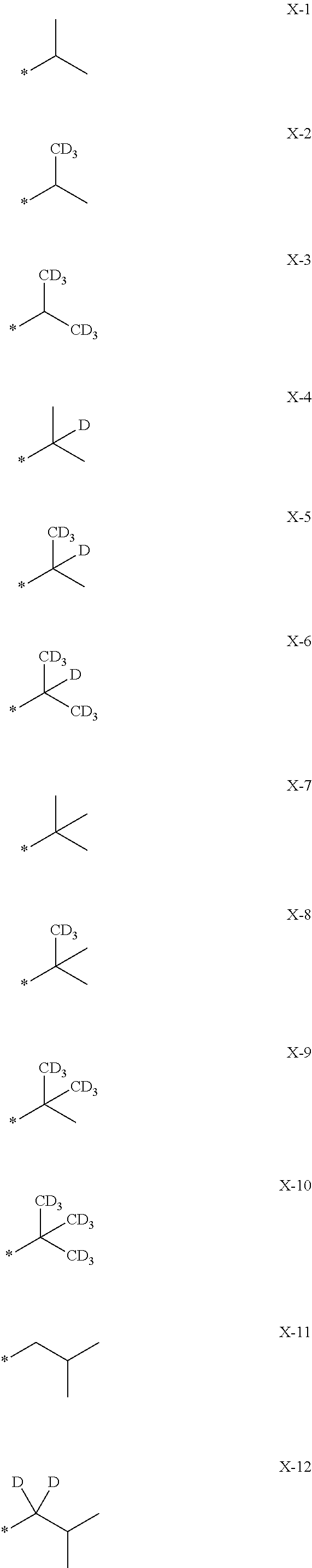


-
- wherein * in Formulae X-1 to X-30 indicates a binding site to a neighboring atom.
- A “deuterated C1-C60 alkyl group,” a “C1-C60 alkyl group that is substituted with (at least one) deuterium,” a “deuterated C1-C20 alkyl group,” or a “C1-C20 alkyl group that is substituted with (at least one) deuterium” as utilized herein may refer to a group represented by a linear or branched C1-C60 alkyl group (or a linear or branched C1-C20 alkyl group) in which at least one hydrogen is substituted with deuterium, and may be, for example, a methyl group, an ethyl group, an n-propyl group, an iso-propyl group, an n-butyl group, a sec-butyl group, an isobutyl group, a tert-butyl group, an n-pentyl group, a tert-pentyl group, a neopentyl group, an isopentyl group, a sec-pentyl group, a 3-pentyl group, a sec-isopentyl group, an n-hexyl group, an iso-hexyl group, a sec-hexyl group, a tert-hexyl group, an n-heptyl group, an iso-heptyl group, a sec-heptyl group, a tert-heptyl group, an n-octyl group, an iso-octyl group, a sec-octyl group, a tert-octyl group, an n-nonyl group, an iso-nonyl group, a sec-nonyl group, a tert-nonyl group, an n-decyl group, an iso-decyl group, a sec-decyl group, or a tert-decyl group, each substituted with at least one deuterium (for example, —CDH2, —CD2H, —CD3, —CDHCH3, —CD2CH3, —CH2CDH2, —CDHCDH2, —CD2CDH2, —CH2CD2H, —CDHCD2H, —CD2CD2H, —CH2CD3, —CDHCD3, —CD2CD3, or a group represented by one of (e.g., one selected from among) Formulae X-2 to X-6, X-8 to X-10, X-12 to X-22, and X-23 to X-30).
- a1, a2, a3, a4, c1, c2, c3, and c4 in Formulae 1 and 1A respectively indicate the numbers of R1, R2, R3, R4, T1, T2, T3, and T4, wherein a1 to a4 may each independently be an integer from 0 to 10 (for example, an integer from 0 to 6), c1 may be an integer from 1 to 3, c2 and c4 may each independently be an integer from 1 to 5, and c3 may be an integer from 1 to 4. When a1 is 2 or more, two or more of R1 may be identical to or different from each other, when a2 is 2 or more, two or more of R2 may be identical to or different from each other, when a3 is 2 or more, two or more of R3 may be identical to or different from each other, when a4 is 2 or more, two or more of R4 may be identical to or different from each other, when c1 is 2 or more, two or more of T1 may be identical to or different from each other, when c2 is 2 or more, two or more of T2 may be identical to or different from each other, when c3 is 2 or more, two or more of T3 may be identical to or different from each other, and when c4 is 2 or more, two or more of T4 may be identical to or different from each other.
- In one or more embodiments, the organometallic compound represented by Formula 1 may satisfy at least one of (e.g., at least one selected from among) Condition A1 to Condition A4:
-
-
- a1 is not 0, and R1 is not hydrogen;
-
-
- a2 is not 0, and R2 is not hydrogen;
-
-
- a3 is not 0, and R3 is not hydrogen; and
-
-
- a4 is not 0, and R4 is not hydrogen.
- In one or more embodiments, the organometallic compound represented by Formula 1 may include at least one deuterium.
- In one or more embodiments, the organometallic compound represented by Formula 1 may satisfy at least one of (e.g., at least one selected from among) Condition B1 to Condition B4:
-
-
- a1 is not 0, and at least one R1 is deuterium or a deuterium-containing group;
-
-
- a2 is not 0, and at least one R2 is deuterium or a deuterium-containing group;
-
-
- a3 is not 0, and at least one R3 is deuterium or a deuterium-containing group; and
-
-
- a4 is not 0, and at least one R4 is deuterium or a deuterium-containing group.
- The “deuterium-containing group” as utilized herein refers to a (e.g., any) group including at least one deuterium, and may be further substituted with substituents other than deuterium. For example, the deuterium-containing group may be a C1-C20 alkyl group, a fluorinated C1-C20 alkyl group, a phenyl group, a fluorinated a phenyl group, a (C1-C20 alkyl)phenyl group, a biphenyl group, a fluorinated biphenyl group, a (C1-C20 alkyl)biphenyl group, a C3-C10 cycloalkyl group, a naphthyl group, a carbazolyl group, a dibenzofuranyl group, or a dibenzothiophenyl group, each substituted with at least one deuterium (for example, —CH2D, —CHD2, —CD3, —C6D5, and/or the like).
- In Formula 1A, a group represented by
-
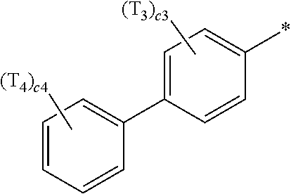
- and a group represented by
-

- may be different from each other. In other words, a group represented by Formula 1A has an asymmetric structure.
- In one or more embodiments, Formula 1A may satisfy one of (e.g., one selected from among) Condition C1 to Condition C3:
- T1 is hydrogen or deuterium;
-
-
- one of T1 is:
- a C1-C20 alkyl group that is unsubstituted or substituted with at least one deuterium; or
- a C6-C20 aryl group (for example, a phenyl group) that is unsubstituted or substituted with deuterium, a C1-C20 alkyl group, a deuterated C1-C20 alkyl group, or a (e.g., any) combination thereof, and the (e.g., any) remaining T1 are hydrogen or deuterium; and
-
-
- two of T1 may each independently be:
- a C1-C20 alkyl group that is unsubstituted or substituted with at least one deuterium; or
- a C6-C20 aryl group (for example, a phenyl group) that is unsubstituted or substituted with deuterium, a C1-C20 alkyl group, a deuterated C1-C20 alkyl group, or a (e.g., any) combination thereof, and
- the (e.g., any) remaining T1 is hydrogen or deuterium.
- In one or more embodiments, Formula 1A may satisfy one of (e.g., one selected from among) Condition D1 to Condition D4:
- T2 is hydrogen or deuterium;
- one of T2 is:
-
- a C1-C20 alkyl group that is unsubstituted or substituted with at least one deuterium; or
- a C6-C20 aryl group (for example, a phenyl group) that is unsubstituted or substituted with deuterium, a C1-C20 alkyl group, a deuterated C1-C20 alkyl group, or a (e.g., any) combination thereof, and
- the (e.g., any) remaining T2 are hydrogen or deuterium;
-
-
- two of T2 may each independently be:
- a C1-C20 alkyl group that is unsubstituted or substituted with at least one deuterium; or
- a C6-C20 aryl group (for example, a phenyl group) that is unsubstituted or substituted with deuterium, a C1-C20 alkyl group, a deuterated C1-C20 alkyl group, or a (e.g., any) combination thereof, and
- the (e.g., any) remaining T2 are hydrogen or deuterium; and
-
-
- three of T2 may each independently be:
- a C1-C20 alkyl group that is unsubstituted or substituted with at least one deuterium; or
- a C6-C20 aryl group (for example, a phenyl group) that is unsubstituted or substituted with deuterium, a C1-C20 alkyl group, a deuterated C1-C20 alkyl group, or a (e.g., any) combination thereof, and
- the (e.g., any) remaining T2 are hydrogen or deuterium.
- In one or more embodiments, Formula 1A may satisfy one of (e.g., one selected from among) Condition E1 to Condition E3:
- T3 is hydrogen or deuterium;
-
-
- one of T3 is:
- a C1-C20 alkyl group that is unsubstituted or substituted with at least one deuterium; or
- a C6-C20 aryl group (for example, a phenyl group) that is unsubstituted or substituted with deuterium, a C1-C20 alkyl group, a deuterated C1-C20 alkyl group, or a (e.g., any) combination thereof, and
- the (e.g., any) remaining T3 are hydrogen or deuterium; and
-
-
- two of T3 may each independently be:
- a C1-C20 alkyl group that is unsubstituted or substituted with at least one deuterium; or
- a C6-C20 aryl group (for example, a phenyl group) that is unsubstituted or substituted with deuterium, a C1-C20 alkyl group, a deuterated C1-C20 alkyl group, or a (e.g., any) combination thereof, and
- the (e.g., any) remaining T3 are hydrogen or deuterium.
- In one or more embodiments, Formula 1A may satisfy one of (e.g., one selected from among) Condition F1 to Condition F4:
- T4 is hydrogen or deuterium;
-
-
- one of T4 is:
- a C1-C20 alkyl group that is unsubstituted or substituted with at least one deuterium; or
- a C6-C20 aryl group (for example, a phenyl group) that is unsubstituted or substituted with deuterium, a C1-C20 alkyl group, a deuterated C1-C20 alkyl group, or a (e.g., any) combination thereof, and
- the (e.g., any) remaining T4 are hydrogen or deuterium;
-
-
- two of T4 may each independently be:
- a C1-C20 alkyl group that is unsubstituted or substituted with at least one deuterium; or
- a C6-C20 aryl group (for example, a phenyl group) that is unsubstituted or substituted with deuterium, a C1-C20 alkyl group, a deuterated C1-C20 alkyl group, or a (e.g., any) combination thereof, and
- the (e.g., any) remaining T4 are hydrogen or deuterium; and
-
-
- three of T4 may each independently be:
- a C1-C20 alkyl group that is unsubstituted or substituted with at least one deuterium; or
- a C6-C20 aryl group (for example, a phenyl group) that is unsubstituted or substituted with deuterium, a C1-C20 alkyl group, a deuterated C1-C20 alkyl group, or a (e.g., any) combination thereof, and
- the (e.g., any) remaining T4 are hydrogen or deuterium.
- In one or more embodiments, Formula 1A may satisfy one selected from among Condition C1 to Condition C3, one selected from among Condition D1 to Condition D4, one selected from among Condition E1 to Condition E3, one selected from among Condition F1 to Condition F4, or a (e.g., any) combination thereof.
- In one or more embodiments, when, in Formula 1A, T1, T3, and T4 are each hydrogen, c2 is 1, and T2 is a tert-butyl group, Formula 1 satisfies Condition G1:
- R4 is:
-
- hydrogen, deuterium, —F, or a cyano group; or
- a C1-C20 alkyl group that is unsubstituted or substituted with deuterium, —F, a cyano group, or a (e.g., any) combination thereof.
- In one or more embodiments, a group represented by
-
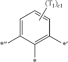
-
-
- i) one of groups represented by Formulae A1-1 to A1-8; or
- ii) one of groups represented by Formulae A1-1 to A1-8 in which at least one hydrogen is substituted with deuterium:
-
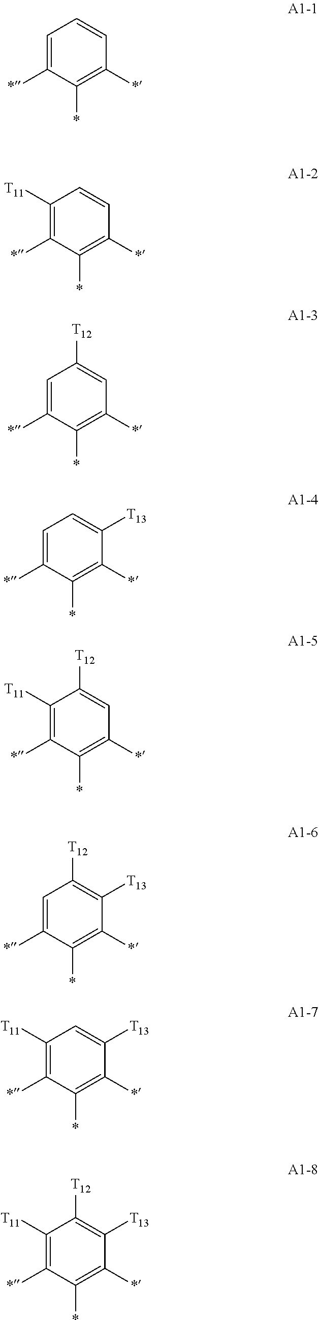
-
- wherein, in Formulae A1-1 to A1-8,
- T11 to T13 may each independently be:
- a C1-C20 alkyl group that is unsubstituted or substituted with at least one deuterium; or
- a C6-C20 aryl group (for example, a phenyl group) that is unsubstituted or substituted with deuterium, a C1-C20 alkyl group, a deuterated C1-C20 alkyl group, or a (e.g., any) combination thereof,
-
- *′ indicates a binding site to a group represented by
-

-
- in Formula 1A, and
- *″ indicates a binding site to a group represented by
-
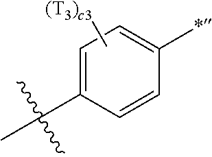
-
- in Formula 1A.
- In one or more embodiments, a group represented by
-

-
-
- i) one of groups represented by Formulae A2-1 to A2-14; or
- ii) one of groups represented by Formulae A2-1 to A2-14 in which at least one hydrogen is substituted with deuterium:
-
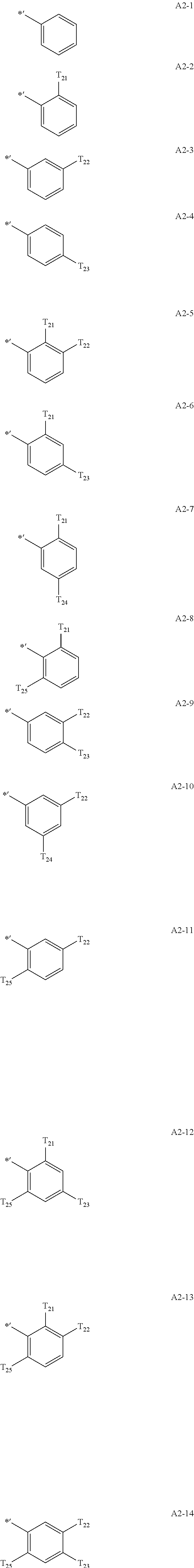
-
- wherein, in Formulae A2-1 to A2-14,
- T21 to T25 may each independently be:
- a C1-C20 alkyl group that is unsubstituted or substituted with at least one deuterium; or
- a C6-C20 aryl group (for example, a phenyl group) that is unsubstituted or substituted with deuterium, a C1-C20 alkyl group, a deuterated C1-C20 alkyl group, or a (e.g., any) combination thereof, and
- *′ indicates a binding site to a group represented by
-

-
- in Formula 1A.
- In one or more embodiments, a group represented by
-

-
-
- i) one of groups represented by Formulae A3-1 to A3-6; or
- ii) one of groups represented by Formulae A3-1 to A3-6 in which at least one hydrogen is substituted with deuterium:
-

-
- wherein, in Formulae A3-1 to A3-6,
- T31 to T34 may each independently be:
- a C1-C20 alkyl group that is unsubstituted or substituted with at least one deuterium; or
- a C6-C20 aryl group (for example, a phenyl group) that is unsubstituted or substituted with deuterium, a C1-C20 alkyl group, a deuterated C1-C20 alkyl group, or a (e.g., any) combination thereof,
- *″ indicates a binding site to a group represented by
-

-
- in Formula 1A, and
- indicates a binding site to a group represented by

-
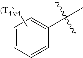
- Formula A3-3 is the same as Formula A3-7
-
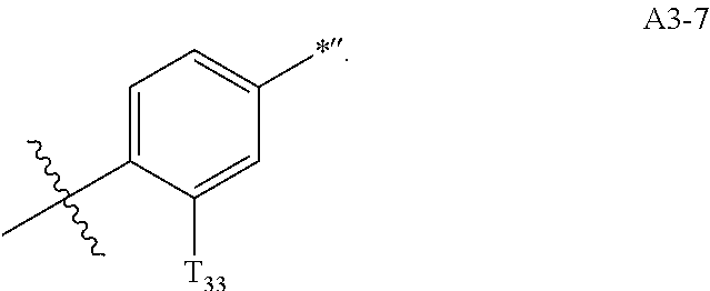
- In one or more embodiments, a group represented by
-
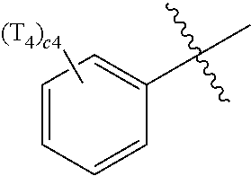
-
-
- i) one of groups represented by Formulae A4-1 to A4-14; or
- ii) one of groups represented by Formulae A4-1 to A4-14 in which at least one hydrogen is substituted with deuterium:
-
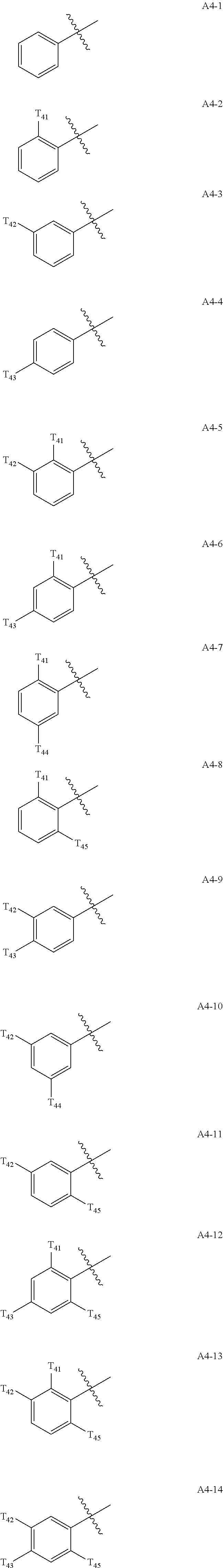
-
- wherein, in Formulae A4-1 to A4-14,
- T41 to T45 may each independently be:
- a C1-C20 alkyl group that is unsubstituted or substituted with at least one deuterium; or
- a C6-C20 aryl group (for example, a phenyl group) that is unsubstituted or substituted with deuterium, a C1-C20 alkyl group, a deuterated C1-C20 alkyl group, or a (e.g., any) combination thereof, and
- indicates a binding site to a group represented by

-
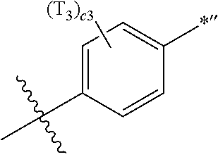
- In one or more embodiments, Ar1 (or a group represented by Formula 1A) may be a C4-C10 alkyl group that is unsubstituted or substituted with at least one deuterium (for example, an n-butyl group, a sec-butyl group, an isobutyl group, a tert-butyl group, an n-pentyl group, a tert-pentyl group, a neopentyl group, an isopentyl group, a sec-pentyl group, a 3-pentyl group, a sec-isopentyl group, an n-hexyl group, an iso-hexyl group, a sec-hexyl group, a tert-hexyl group, an n-heptyl group, an iso-heptyl group, a sec-heptyl group, a tert-heptyl group, an n-octyl group, an iso-octyl group, a sec-octyl group, a tert-octyl group, an n-nonyl group, an iso-nonyl group, a sec-nonyl group, a tert-nonyl group, an n-decyl group, an iso-decyl group, a sec-decyl group, or a tert-decyl group, each unsubstituted or substituted with at least one deuterium, or in one or more embodiments, a group represented by one of Formulae X-7 to X-30), and the number of the C4-C10 alkyl group that is unsubstituted or substituted with at least one deuterium, included in Ar1, may be 2 or more (for example, 2 to 15).
- In one or more embodiments, Ar1 in Formula 1 may be:
-
- i) one of (e.g., selected from among) groups represented by Formulae TP-1 to TP-228; or
- ii) one of (e.g., selected from among) groups represented by Formulae TP-1 to TP-228 in which at least one hydrogen is substituted with deuterium:
-

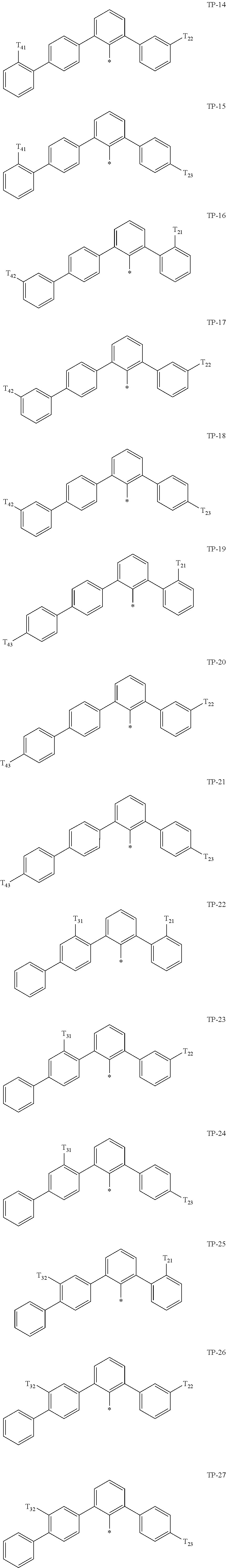

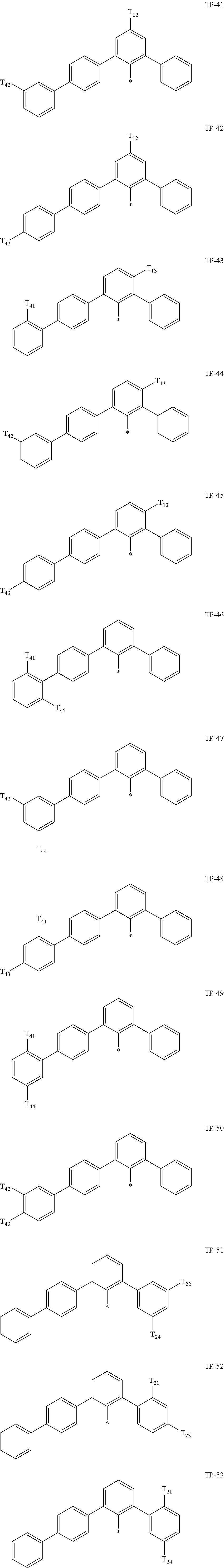
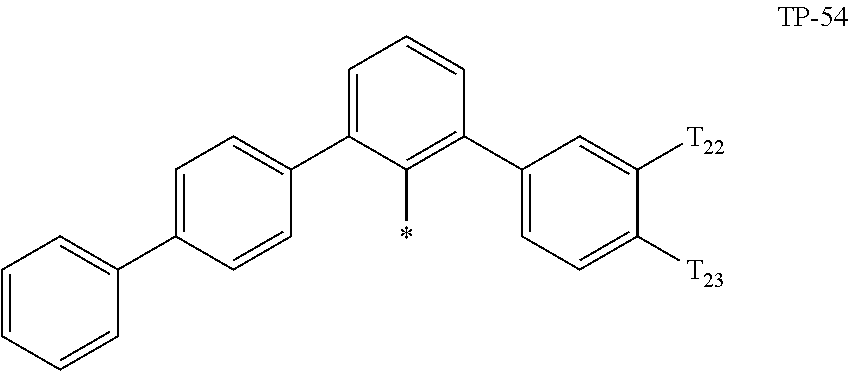
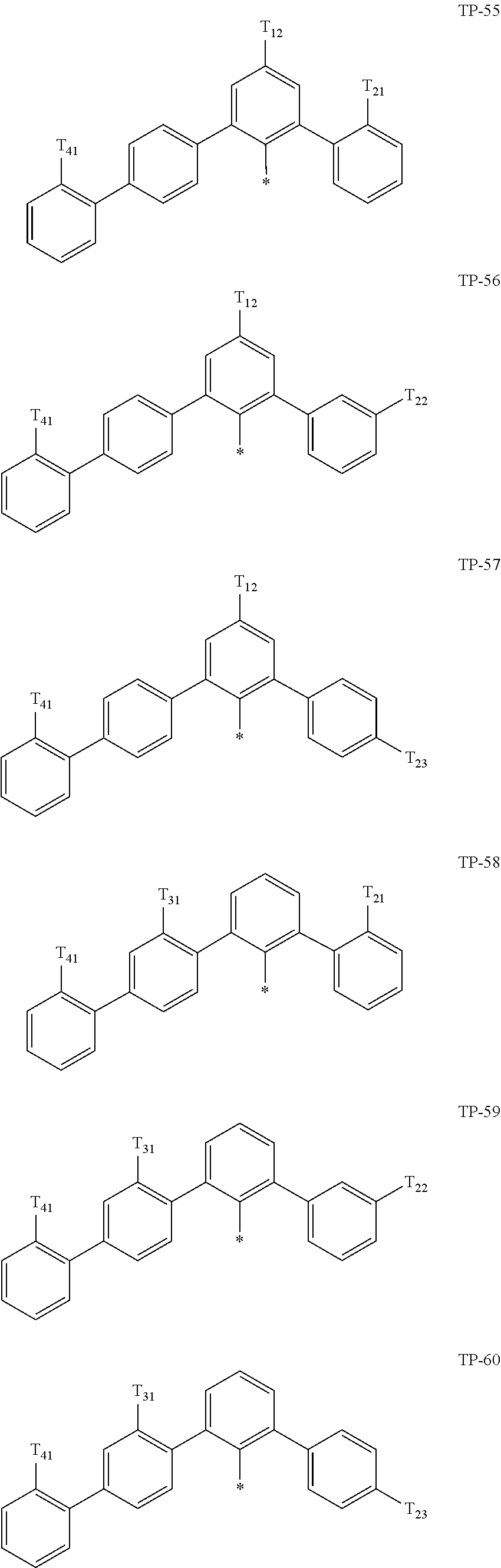

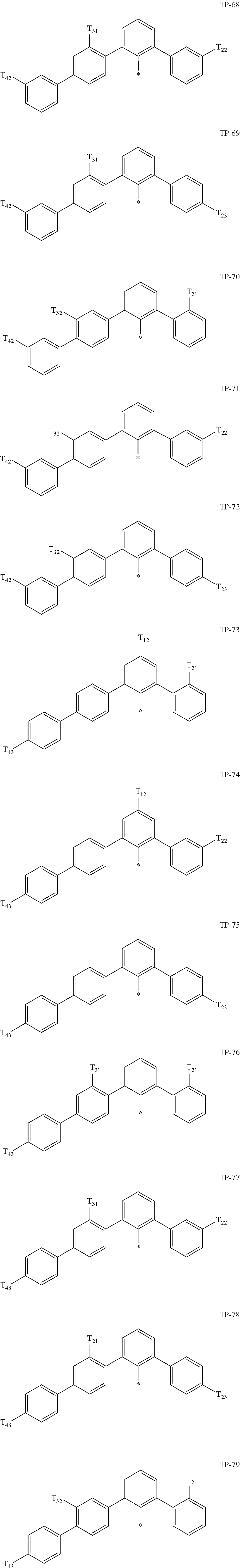

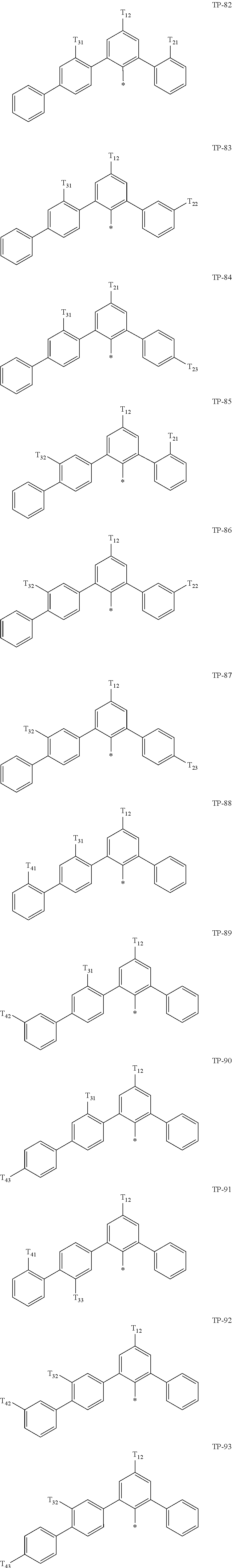
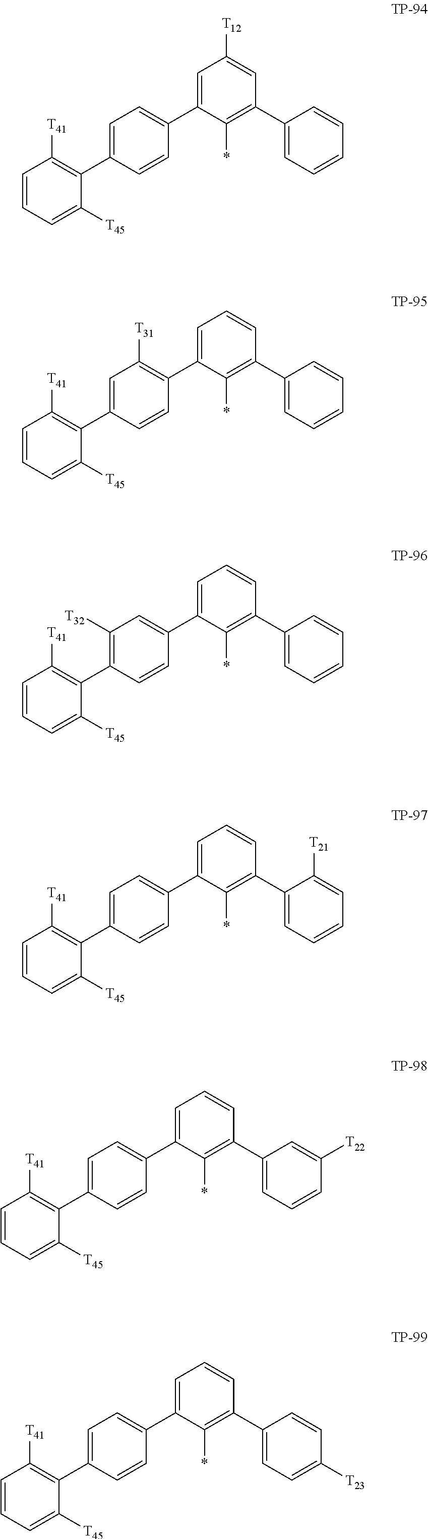
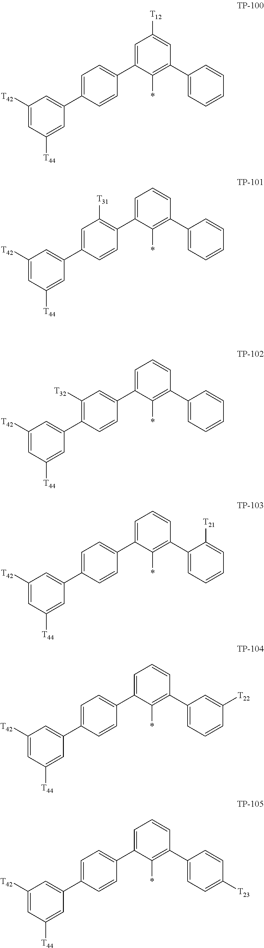
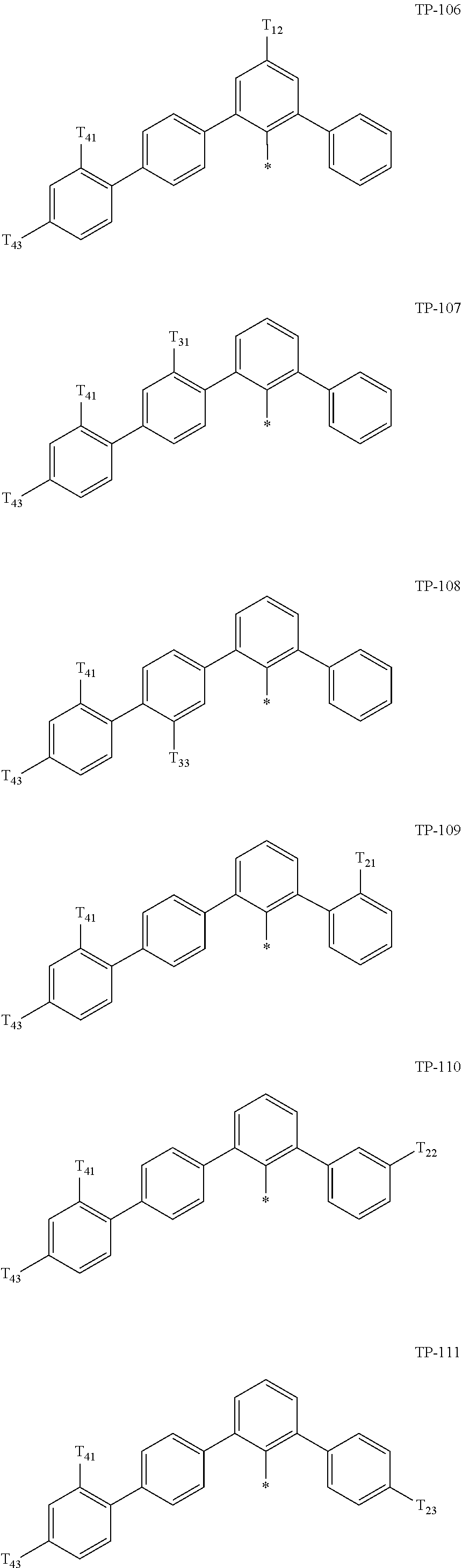
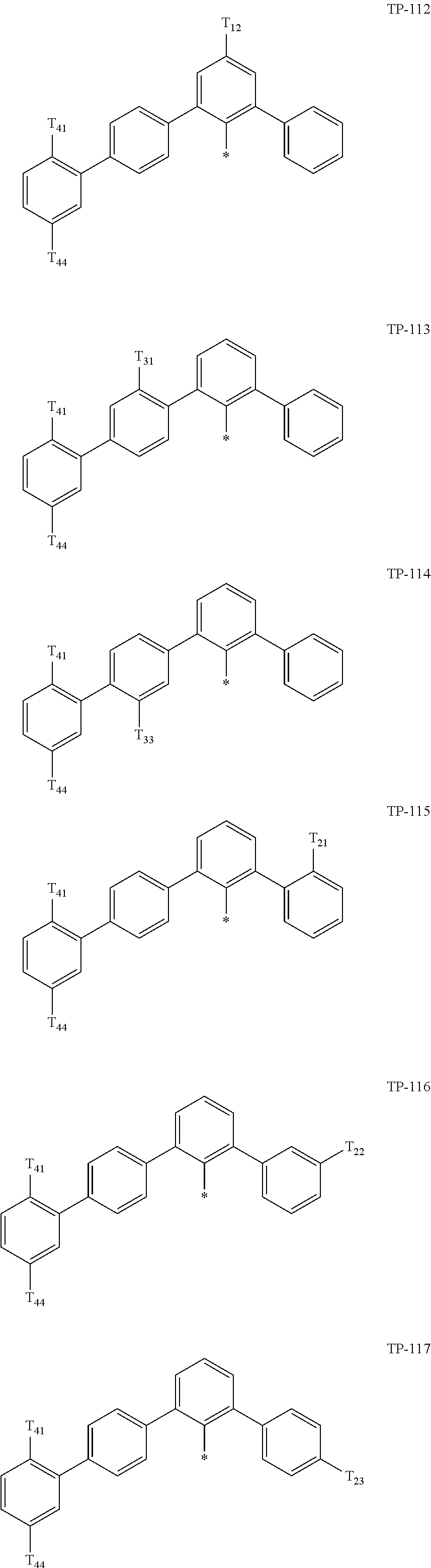


-
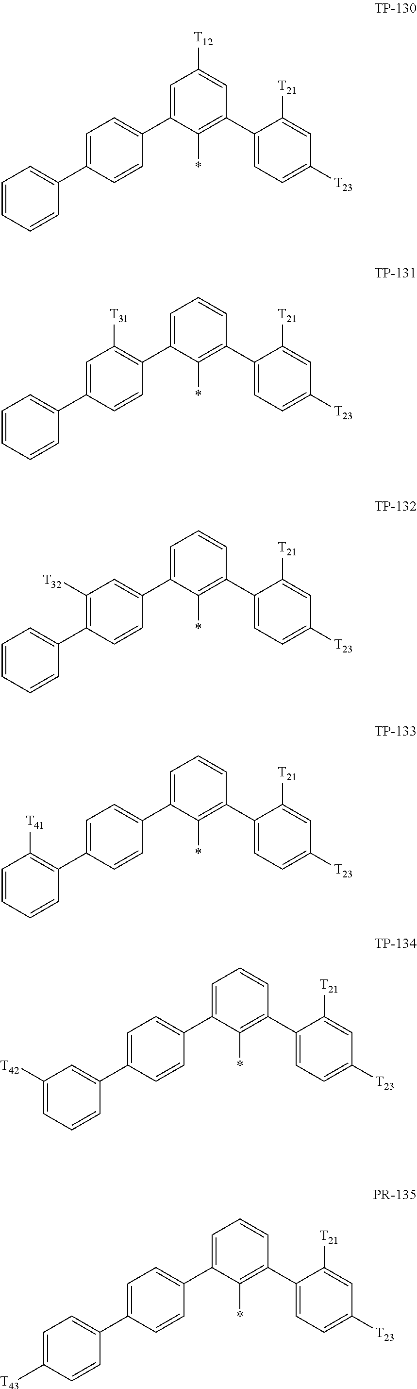
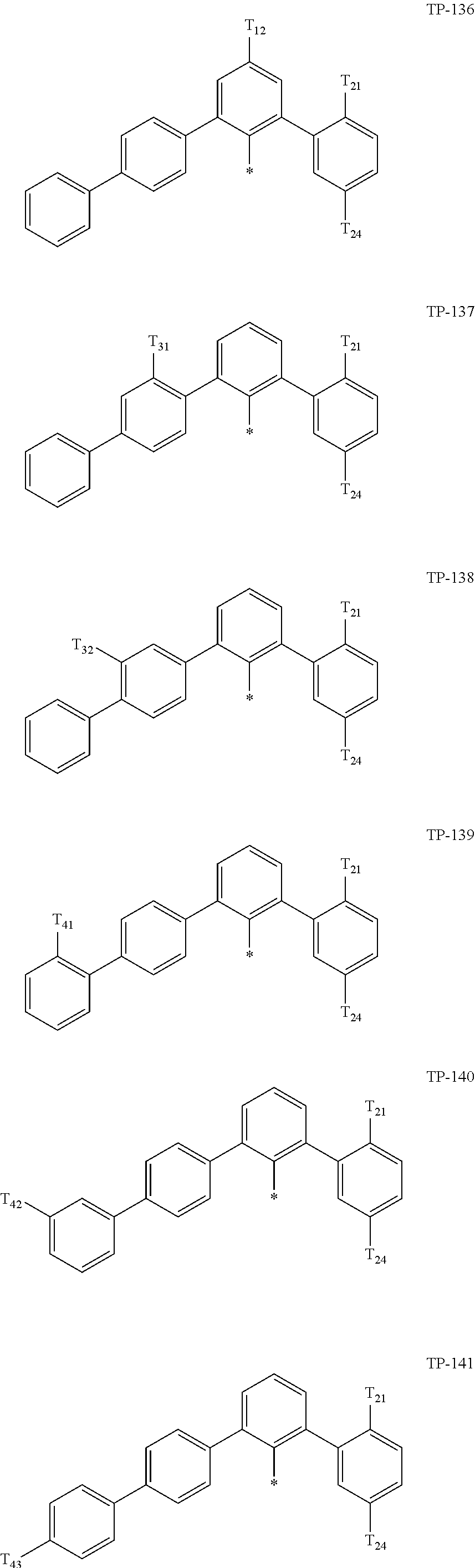
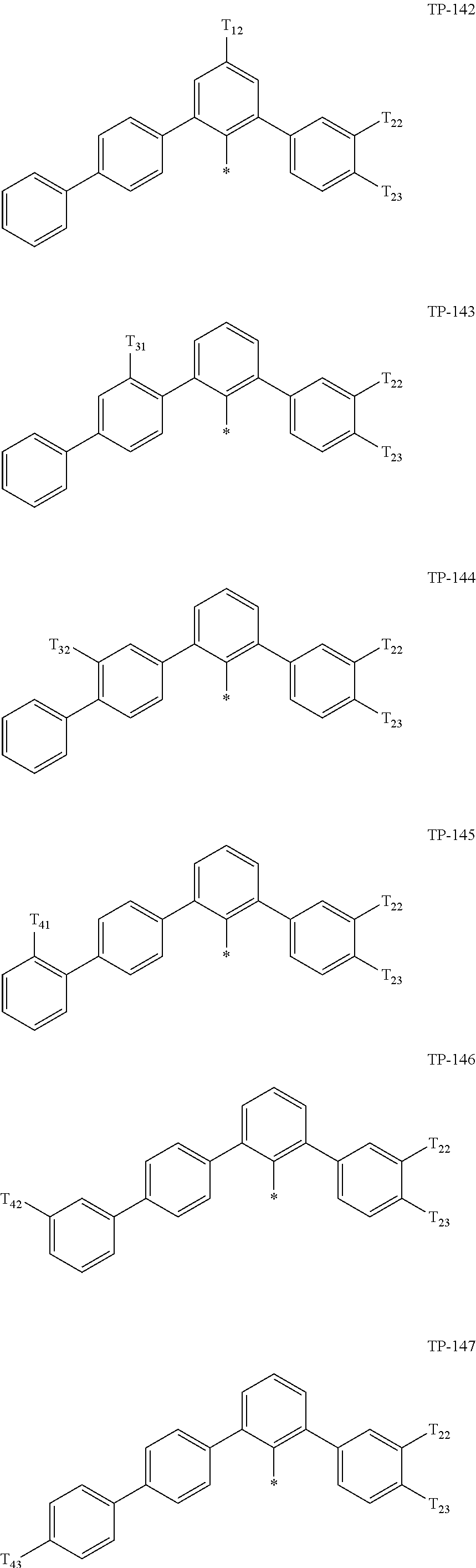

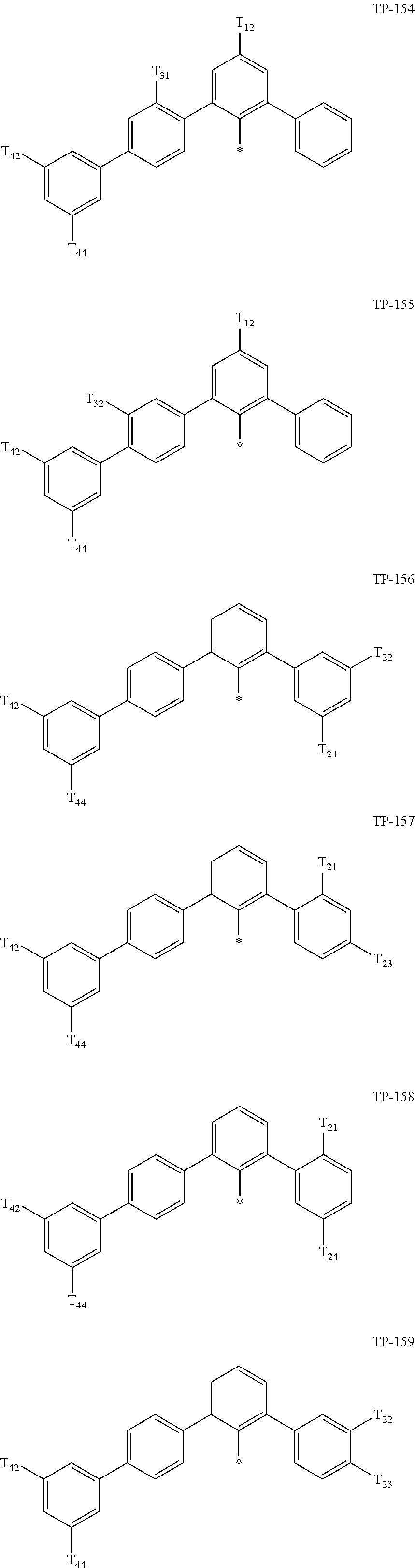
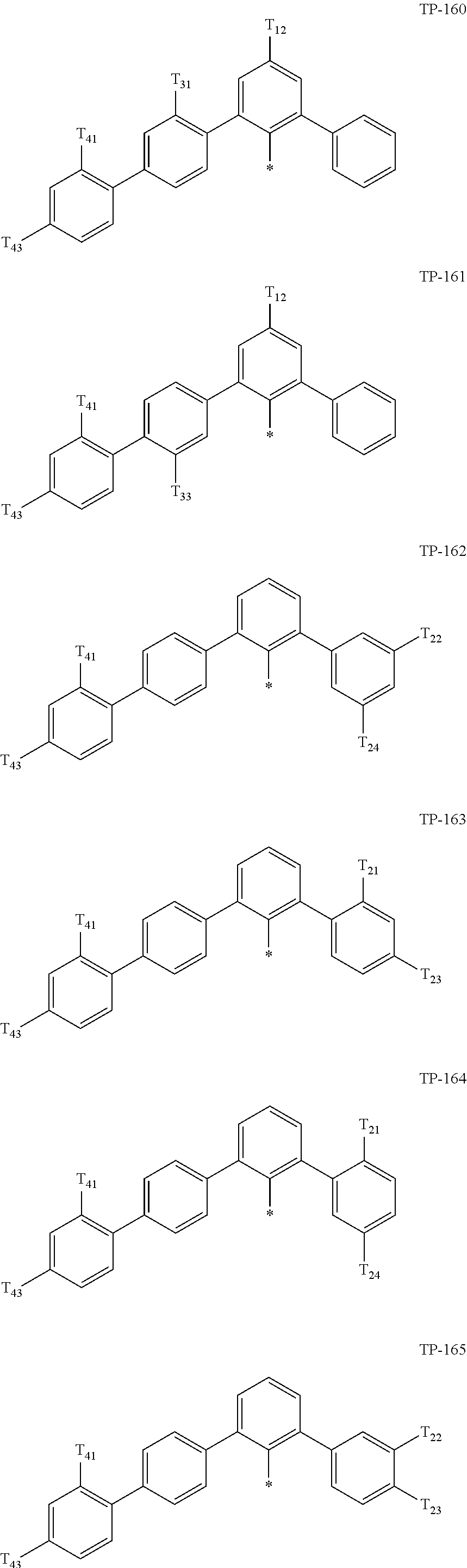


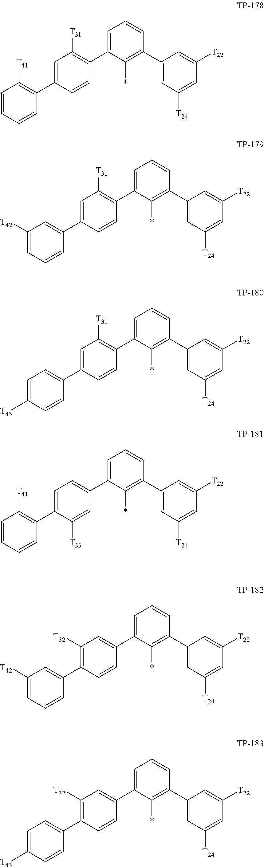

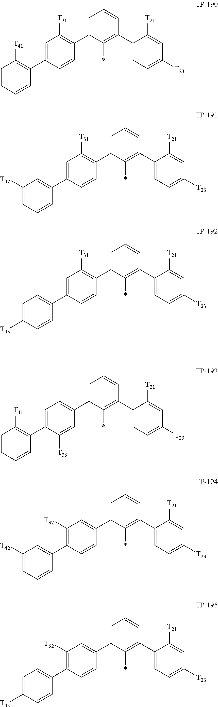
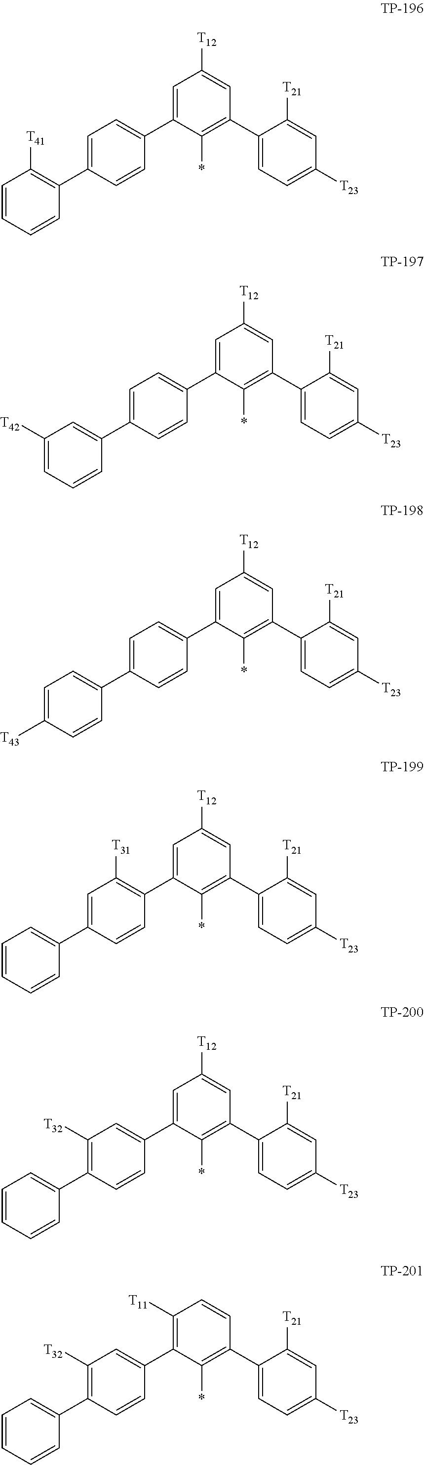

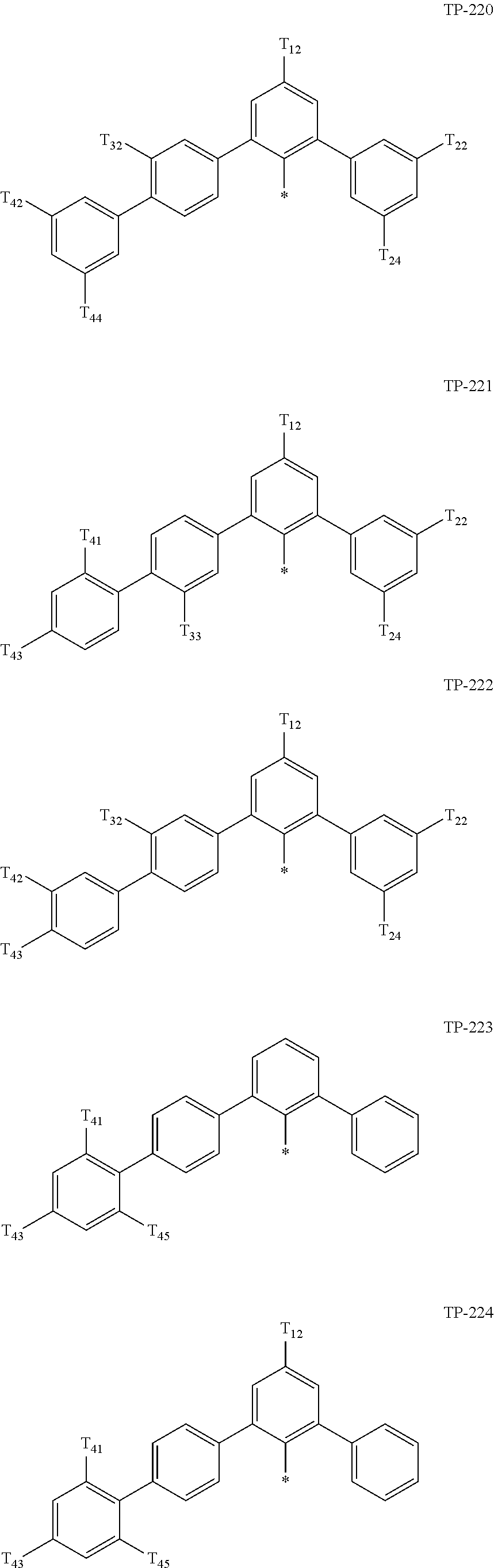
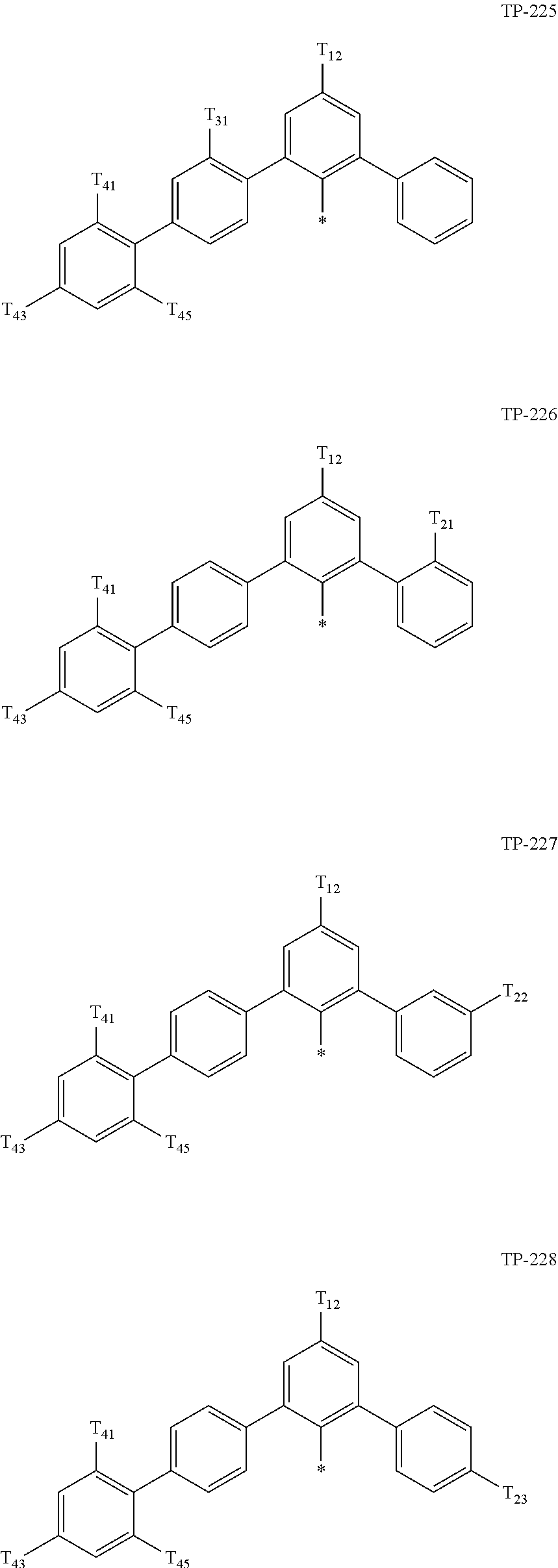
-
- wherein, in Formulae TP-1 to TP-228,
- T11 to T13, T21 to T24, T31 to T33, and T41 to T45 may each independently be:
- a C1-C20 alkyl group that is unsubstituted or substituted with at least one deuterium; or
- a C6-C20 aryl group (for example, a phenyl group) that is unsubstituted or substituted with deuterium, a C1-C20 alkyl group, a deuterated C1-C20 alkyl group, or a (e.g., any) combination thereof, and
- *′ indicates a binding site to ring CY1 in Formula 1.
- The expression “one of groups represented by Formula X in which at least one hydrogen is substituted with deuterium” refers to a group in which at least one of “all” hydrogen present in Formula X is substituted with deuterium.
- For example, examples of “a group represented by Formula TP-51 in which at least one hydrogen is substituted with deuterium” may include (e.g., be represented by) Formulae TP-51(1) to TP-51(6):
-
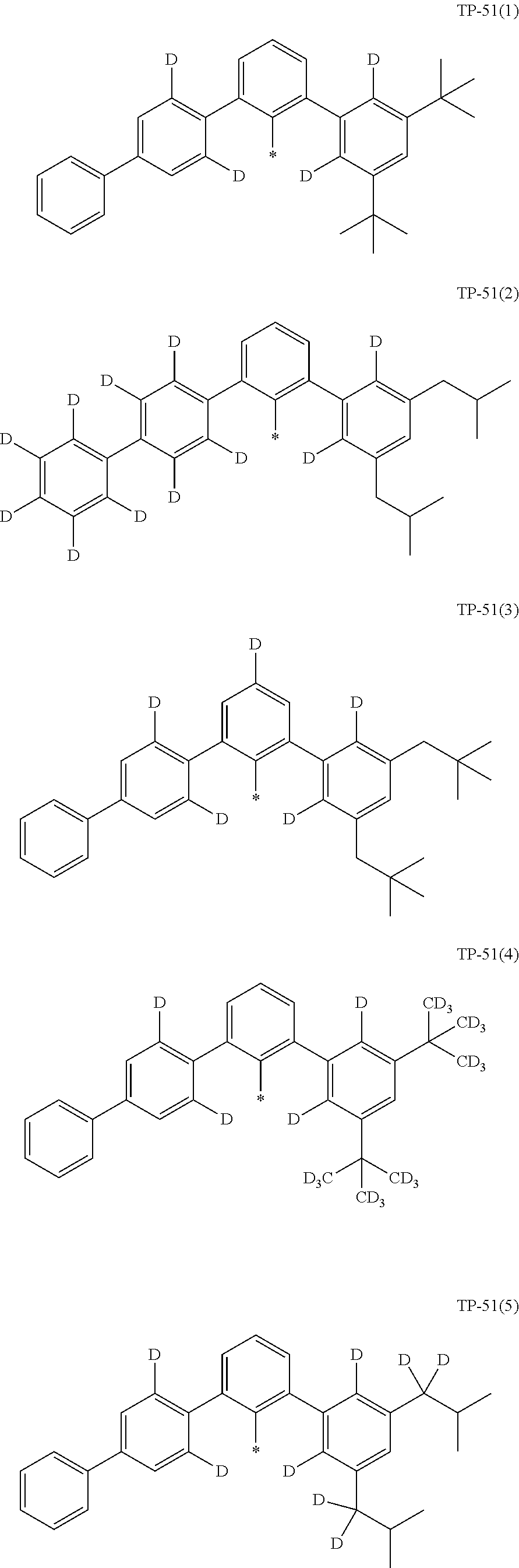

-
- wherein two or more selected from among R1, R2, R3, R4, Z51a, Z51b, Z52a, Z52b, T1, T2, T3, and T4 in Formulae 1 and 1A may optionally be bonded together to form a C3-C60 carbocyclic group that is unsubstituted or substituted with at least one R10a or a C1-C60 heterocyclic group that is unsubstituted or substituted with at least one R10a.
- “*” as utilized herein indicates a binding site to a neighboring atom, unless otherwise stated.
- In one or more embodiments, the organometallic compound represented by Formula 1 may be an organometallic compound represented by Formula 1-1 or an organometallic compound represented by Formula 1-2:
-
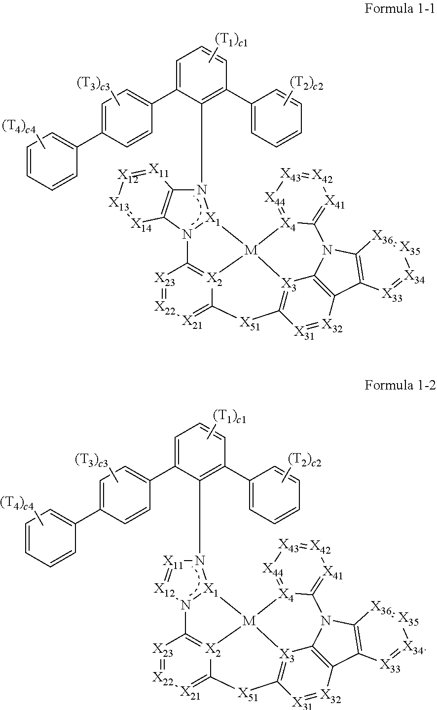
-
- M, X1 to X4, X51, T1 to T4, and c1 to c4 are each as described herein,
- X11 may be C(R11) or N, X12 may be C(R12) or N, X13 may be C(R13) or N, and X14 may be C(R14) or N,
- R11 to R14 are each as described in connection with R1, and two or more R11 to R14 may optionally be bonded together to form a C3-C60 carbocyclic group that is unsubstituted or substituted with at least one R10a or a C1-C60 heterocyclic group that is unsubstituted or substituted with at least one R10a,
- X21 may be C(R21) or N, X22 may be C(R22) or N, and X23 may be C(R23) or N,
- R21 to R23 are each as described in connection with R2, and two or more R21 to R23 may optionally be bonded together to form a C3-C60 carbocyclic group that is unsubstituted or substituted with at least one R10a or a C1-C60 heterocyclic group that is unsubstituted or substituted with at least one R10a,
- X31 may be C(R31) or N, X32 may be C(R32) or N, X33 may be C(R33) or N, X34 may be C(R34) or N, X35 may be C(R35) or N, and X36 may be C(R36) or N,
- R31 to R36 are each as described in connection with R3, and two or more R31 to R36 may optionally be bonded together to form a C3-C60 carbocyclic group that is unsubstituted or substituted with at least one R10a or a C1-C60 heterocyclic group that is unsubstituted or substituted with at least one R10a,
- X41 may be C(R41) or N, X42 may be C(R42) or N, X43 may be C(R43) or N, and X44 may be C(R44) or N,
- R41 to R44 are each as described in connection with R4, and two or more R41 to R44 may optionally be bonded together to form a C3-C60 carbocyclic group that is unsubstituted or substituted with at least one R10a or a C1-C60 heterocyclic group that is unsubstituted or substituted with at least one R10a,
- a group represented by
-
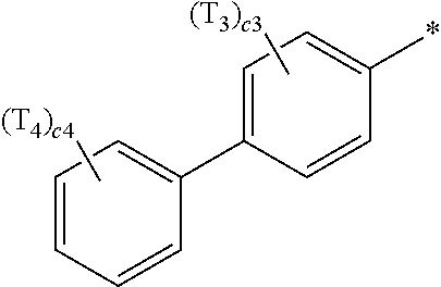
- and a group represented by
-
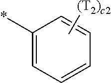
- may be different from each other, and
-
- * indicates a binding site to a neighboring atom.
- The description of Formula 1 may be applied to Formulae 1-1 and 1-2.
- Descriptions of Ar1 and descriptions of Formula 1A may be applied to a group represented by
-
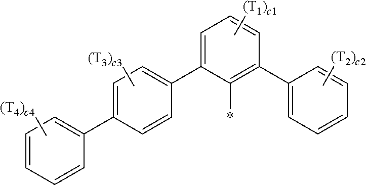
- In one or more embodiments, X43 in Formula 1-1 and 1-2 may be C(R43), wherein R43 may be:
-
- hydrogen, deuterium, —F, or a cyano group; or
- a C1-C20 alkyl group that is unsubstituted or substituted with deuterium, —F, a cyano group, or a (e.g., any) combination thereof.
- In one or more embodiments, when, in Formulae 1-1 and 1-2, T1, T3, and T4 are each hydrogen, c2 is 1, and T2 is a tert-butyl group, then Formulae 1-1 and 1-2 may satisfy Condition G2:
-
-
- X43 is C(R43),
- wherein R43 is:
- hydrogen, deuterium, —F, or a cyano group; or
- a C1-C20 alkyl group that is unsubstituted or substituted with deuterium, —F, a cyano group, or a (e.g., any) combination thereof.
- In one or more embodiments, in Formulae 1-1 and 1-2, X11 may be C(R11), X12 may be C(R12), X13 may be C(R13), X14 may be C(R14), X21 may be C(R21), X22 may be C(R22), X23 may be C(R23), X31 may be C(R31), X32 may be C(R32), X33 may be C(R33), X34 may be C(R34), X35 may be C(R35), X36 may be C(R36), X41 may be C(R41), X42 may be C(R42), and X43 may be C(R43), R11 to R14, R21 to R23, R31 to R36, and R41 to R43 may be the same as described herein, and
-
- Each of Formulae 1-1 and 1-2 may satisfy at least one selected from among Condition H1 to Condition H4:
-
-
- at least one of R11 to R14 in Formula 1-1 is deuterium or a deuterium-containing group, and at least one of R11 and R12 in Formula 1-2 is deuterium or a deuterium-containing group;
-
-
- at least one of R21 to R23 is deuterium or a deuterium-containing group;
-
-
- at least one of R31 to R36 is deuterium or a deuterium-containing group; and
-
-
- at least one of R41 to R44 is deuterium or a deuterium-containing group.
- In one or more embodiments, a group represented by
-

- in Formula 1 may be a group represented by one of Formulae CY1-1 to CY1-42:
-


-
- wherein, in Formulae CY1-1 to CY1-42,
- X1 is as described herein,
- Y1 may include O, S, N, C, or Si,
- * indicates a binding site to M in Formula 1, and
- *′ indicates a binding site to a neighboring atom in Formula 1.
- In one or more embodiments, X1 in Formulae CY1-1 to CY1-8 may be C, and X1 in Formulae CY1-9 to CY1-42 may be N.
- In one or more embodiments, a group represented by
-

- in Formula 1 may be a group represented by one of Formulae CY2-1 to CY2-11:
-

-
- wherein, in Formulae CY2-1 to CY2-11,
- X2 is as described herein,
- Y2 may include O, S, N, C, or Si,
- * indicates a binding site to M in Formula 1,
- *′ indicates a binding site to ring CY1 in Formula 1, and
- *″ indicates a binding site to X51 in Formula 1.
- In one or more embodiments, a group represented by
-
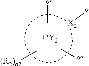
- in Formula land a group represented by
-
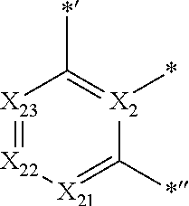
- in Formulae 1-1 and 1-2 may each independently be a group represented by one of Formulae CY2(1) to CY2(26):
-


-
- wherein, in Formulae CY2(1) to CY2(26),
- X2 is as described herein,
- X21 may be O, S, N(R20), C(R20a)(R20b), or Si(R20a)(R20b),
- R20, R20a, R20b, and R21 to R23 are each as described in connection with R2, and R21 to R23 may each not be hydrogen,
- * indicates a binding site to M in Formula 1,
- *′ indicates a binding site to ring CY1 in Formula 1, and
- *″ indicates a binding site to X51 in Formula 1.
- In one or more embodiments, a group represented by
-
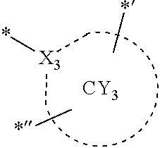
- in Formula 1 may be a group represented by one of Formulae CY3-1 to CY3-23:
-


-
- wherein, in Formulae CY3-1 to CY3-23,
- X3 is as described herein,
- Y3 may include O, S, N, C, or Si,
- * indicates a binding site to M in Formula 1,
- *′ indicates a binding site to X52 in Formula 1, and
- *″ indicates a binding site to X51 in Formula 1.
- In one or more embodiments, a group represented by
-
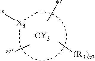
- in Formula 1 may be a group represented by one of Formulae CY3(1) to CY3(20), and a group represented by
-
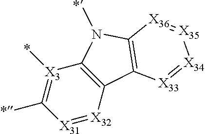
- in Formulae 1-1 and 1-2 may be a group represented by one of Formulae CY3(1) to CY3 (12):
-

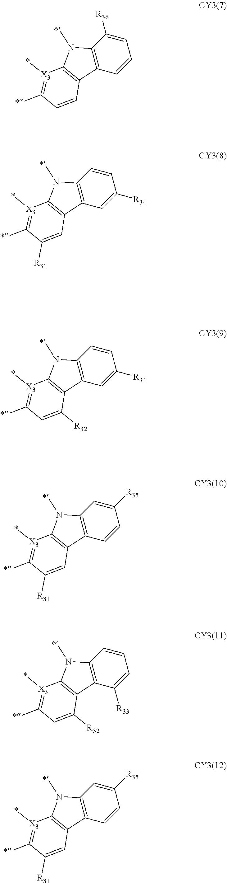

-
- wherein, in Formulae CY3(1) to CY3(20),
- X3 is as described herein,
- R31 to R36 are each as described in connection with R3, wherein R31 to R36 may each not be hydrogen,
- * indicates a binding site to M in Formula 1,
- *′ indicates a binding site to X52 in Formula 1, and
- *″ indicates a binding site to X51 in Formula 1.
- In one or more embodiments, a group represented by
-
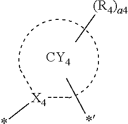
- in Formula 1 may be a group represented by one of CY4(1) to CY4(16):
-

-
- wherein, in Formulae CY4(1) to CY4(16),
- X4 is as described herein,
- R41 to R44 are each as described in connection with R4, and R41 to R44 may each not be hydrogen,
- * indicates a binding site to M in Formula 1, and
- *′ indicates a binding site to X52 in Formula 1.
- Ar1 in Formula 1 may be a group represented by Formula 1A:
-

-
- wherein, Formula 1A includes a “Benzene group 4” bonded to the para-position in a “
Benzene group 3” with respect to carbon which is bonded to a “Benzene group 1.” In some embodiments, in Formula 1A, a group represented by
- wherein, Formula 1A includes a “Benzene group 4” bonded to the para-position in a “
-
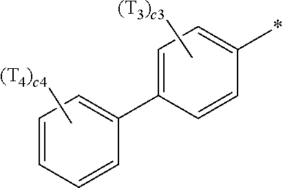
-
- and a group represented by
-

-
- may be different from each other. In other words, Formula 1A has an asymmetric structure with respect to the axis of symmetry.
- Accordingly, 1) the intramolecular movement of Formula 1A is suppressed or reduced and Stoke's shift is reduced, thereby increasing the PLQY of the organometallic compound represented by Formula 1, 2) during formation of a film including the organometallic compound, the intramolecular packing effect is reduced, thereby lowering the sublimation temperature and deposition temperature, and 3) interference between other substituents in the molecule of the organometallic compound is minimized or reduced by the “
Benzene group 3” and the “Benzene group 4.” Thus, the non-radiative decay rate (Knr) and Dexter energy transfer of a light-emitting device including the organometallic compound represented by Formula 1 are reduced, and thus, the luminescence efficiency and/or lifespan of the light-emitting device may be improved. - In one or more embodiments, Formula 1A may further include at least one C1-C20 alkyl group that is unsubstituted or substituted with deuterium. Accordingly, the asymmetry and bulkiness of Formula 1A may be increased, and thus, the luminescence efficiency and/or lifespan of a light-emitting device including the organometallic compound may be further improved.
- In one or more embodiments, b51 to b53 in
Formula 2 indicate the number of L51 to the number of L53, respectively, and may each be an integer from 1 to 5. When b51 is 2 or more, two or more of L51 may be identical to or different from each other, when b52 is 2 or more, two or more of L52 may be identical to or different from each other, and when b53 is 2 or more, two or more of L53 may be identical to or different from each other. In one or more embodiments, b51 to b53 may each independently be 1 or 2. - L51 to L53 in
Formula 2 may each independently be: -
- a single bond; or
- a benzene group, a naphthalene group, an anthracene group, a phenanthrene group, a triphenylene group, a pyrene group, a chrysene group, a cyclopentadiene group, a furan group, a thiophene group, a silole group, an indene group, a fluorene group, an indole group, a carbazole group, a benzofuran group, a dibenzofuran group, a benzothiophene group, a dibenzothiophene group, a benzosilole group, a dibenzosilole group, an azafluorene group, an azacarbazole group, an azadibenzofuran group, an azadibenzothiophene group, an azadibenzosilole group, a pyridine group, a pyrimidine group, a pyrazine group, a pyridazine group, a triazine group, a quinoline group, an isoquinoline group, a quinoxaline group, a quinazoline group, a phenanthroline group, a pyrrole group, a pyrazole group, an imidazole group, a triazole group, an oxazole group, an isoxazole group, a thiazole group, an isothiazole group, an oxadiazole group, a thiadiazole group, a benzopyrazole group, a benzimidazole group, a benzoxazole group, a benzothiazole group, a benzoxadiazole group, a benzothiadiazole group, a dibenzooxacilline group, a dibenzothiacilline group, a dibenzodihydroazacilline group, a dibenzodihydrodicilline group, a dibenzodihydrocilline group, a dibenzodioxane group, a dibenzooxathiene group, a dibenzooxazine group, a dibenzopyran group, a dibenzodithiine group, a dibenzothiazine group, a dibenzothiopyran group, a dibenzocyclohexadiene group, a dibenzodihydropyridine group, or a dibenzodihydropyrazine group, each unsubstituted or substituted with deuterium, —F, —Cl, —Br, —I, a hydroxyl group, a cyano group, a nitro group, a C1-C20 alkyl group, a C1-C20 alkoxy group, a phenyl group, a naphthyl group, a pyridinyl group, a pyrimidinyl group, a triazinyl group, a fluorenyl group, a dimethylfluorenyl group, a diphenylfluorenyl group, a carbazolyl group, a phenylcarbazolyl group, a dibenzofuranyl group, a dibenzothiophenyl group, a dibenzosilolyl group, a dimethyldibenzosilolyl group, a diphenyldibenzosilolyl group, —O(Q31), —S(Q31), —Si(Q31)(Q32)(Q33), —N(Q31)(Q32), —B(Q31)(Q32), —P(Q31)(Q32), —C(═O)(Q31), —S(═O)2(Q31), —P(═O)(Q31)(Q32), or a (e.g., any) combination thereof, and
- Q31 to Q33 may each independently be hydrogen, deuterium, a C1-C20 alkyl group, a C1-C20 alkoxy group, a phenyl group, a biphenyl group, a terphenyl group, a pyridinyl group, a pyrimidinyl group, a pyridazinyl group, a pyrazinyl group, or a triazinyl group.
- In one or more embodiments, in
Formula 2, a bond between L51 and R51, a bond between L52 and R52, a bond between L53 and R53, a bond between two or more L51, a bond between two or more L52, a bond between two or more L53, a bond between L51 and carbon between X54 and X55 inFormula 2, a bond between L52 and carbon between X54 and X56 inFormula 2, and a bond between L53 and carbon between X55 and X56 inFormula 2 may each be a “carbon-carbon single bond.” - In
Formula 2, X54 may be N or C(R54), X55 may be N or C(R55), X56 may be N or C(R56), and at least one of X54 to X56 may be N. R54 to R56 are each as described herein. In one or more embodiments, two or three of X54 to X56 may be N. - R51 to R56, R71 to R74, R81 to R85, R82a, R82b, R83a, R83b, R84a, R84b, R500a, R500b, R501 to R508, R505a, R505b, R506a, R506b, R507a, R507b, R508a, and R508b as utilized herein may each independently be hydrogen, deuterium, —F, —Cl, —Br, —I, a hydroxyl group, a cyano group, a nitro group, a C1-C60 alkyl group that is unsubstituted or substituted with at least one R10a, a C2-C60 alkenyl group that is unsubstituted or substituted with at least one R10a, a C2-C60 alkynyl group that is unsubstituted or substituted with at least one R10a, a C1-C60 alkoxy group that is unsubstituted or substituted with at least one R10a, a C3-C60 carbocyclic group that is unsubstituted or substituted with at least one R10a, a C1-C60 heterocyclic group that is unsubstituted or substituted with at least one R10a, a C6-C60 aryloxy group that is unsubstituted or substituted with at least one R10a, a C6-C60 arylthio group that is unsubstituted or substituted with at least one R10a, a C7-C60 arylalkyl group that is unsubstituted or substituted with at least one R10a, a C2-C60 heteroarylalkyl group that is unsubstituted or substituted with at least one R10a, —C(Q1)(Q2)(Q3), —Si(Q1)(Q2)(Q3), —N(Q1)(Q2), —B(Q1)(Q2), —C(═O)(Q1), —S(═O)2(Q1), or —P(═O)(Q1)(Q2). Q1 to Q3 are each as described herein.
- For example, i) R1 to R4, Z51a, Z51b, Z52a, Z52b, and T1 to T4 in Formula 1, ii) R51 to R56, R71 to R74, R81 to R85, R82a, R82b, R83a, R83b, R84a and R84b, R500a, R500b, R501 to R508, R505a, R505b, R506a, R506b, R507a, R507b, R508a, and R508b in
Formulae 2, 3-1 to 3-5, 502, and 503, and iii) R10a may each independently be: -
- hydrogen, deuterium, —F, —Cl, —Br, —I, a hydroxyl group, a cyano group, a nitro group, a C1-C20 alkyl group, or a C1-C20 alkoxy group;
- a C1-C20 alkyl group or a C1-C20 alkoxy group, each substituted with deuterium, —F, —Cl, —Br, —I, —CD3, —CD2H, —CDH2, —CF3, —CF2H, —CFH2, a hydroxyl group, a cyano group, a nitro group, a C1-C10 alkyl group, a cyclopentyl group, a cyclohexyl group, a cycloheptyl group, a cyclooctyl group, an adamantanyl group, a norbornanyl group, a norbornenyl group, a cyclopentenyl group, a cyclohexenyl group, a cycloheptenyl group, a phenyl group, a biphenyl group, a naphthyl group, a pyridinyl group, a pyrimidinyl group, or a (e.g., any) combination thereof;
- a cyclopentyl group, a cyclohexyl group, a cycloheptyl group, a cyclooctyl group, an adamantanyl group, a norbornanyl group, a norbornenyl group, a cyclopentenyl group, a cyclohexenyl group, a cycloheptenyl group, a phenyl group, a biphenyl group, a C1-C10 alkylphenyl group, a naphthyl group, a fluorenyl group, a phenanthrenyl group, an anthracenyl group, a fluoranthenyl group, a triphenylenyl group, a pyrenyl group, a chrysenyl group, a pyrrolyl group, a thiophenyl group, a furanyl group, an imidazolyl group, a pyrazolyl group, a thiazolyl group, an isothiazolyl group, an oxazolyl group, an isoxazolyl group, a pyridinyl group, a pyrazinyl group, a pyrimidinyl group, a pyridazinyl group, an isoindolyl group, an indolyl group, an indazolyl group, a purinyl group, a quinolinyl group, an isoquinolinyl group, a benzoquinolinyl group, a quinoxalinyl group, a quinazolinyl group, a cinnolinyl group, a carbazolyl group, a phenanthrolinyl group, a benzoimidazolyl group, a benzofuranyl group, a benzothiophenyl group, a benzoisothiazolyl group, a benzoxazolyl group, a benzoisoxazolyl group, a triazolyl group, a tetrazolyl group, an oxadiazolyl group, a triazinyl group, a dibenzofuranyl group, a dibenzothiophenyl group, a benzocarbazolyl group, a dibenzocarbazolyl group, an imidazopyridinyl group, an imidazopyrimidinyl group, an azacarbazolyl group, an azadibenzofuranyl group, an azadibenzothiophenyl group, an azafluorenyl group, an azadibenzosilolyl group, or a group represented by Formula 91, each unsubstituted or substituted with deuterium, —F, —Cl, —Br, —I, —CD3, —CD2H, —CDH2, —CF3, —CF2H, —CFH2, a hydroxyl group, a cyano group, a nitro group, a C1-C20 alkyl group, a C1-C20 alkoxy group, a cyclopentyl group, a cyclohexyl group, a cycloheptyl group, a cyclooctyl group, an adamantanyl group, a norbornanyl group, a norbornenyl group, a cyclopentenyl group, a cyclohexenyl group, a cycloheptenyl group, a phenyl group, a biphenyl group, a C1-C10 alkylphenyl group, a naphthyl group, a fluorenyl group, a phenanthrenyl group, an anthracenyl group, a fluoranthenyl group, a triphenylenyl group, a pyrenyl group, a chrysenyl group, a pyrrolyl group, a thiophenyl group, a furanyl group, an imidazolyl group, a pyrazolyl group, a thiazolyl group, an isothiazolyl group, an oxazolyl group, an isoxazolyl group, a pyridinyl group, a pyrazinyl group, a pyrimidinyl group, a pyridazinyl group, an isoindolyl group, an indolyl group, an indazolyl group, a purinyl group, a quinolinyl group, an isoquinolinyl group, a benzoquinolinyl group, a quinoxalinyl group, a quinazolinyl group, a cinnolinyl group, a carbazolyl group, a phenanthrolinyl group, a benzoimidazolyl group, a benzofuranyl group, a benzothiophenyl group, a benzothiazolyl group, a benzoisoxazolyl group, a benzoisoxazolyl group, a triazolyl group, a tetrazolyl group, an oxadiazolyl group, a triazinyl group, a dibenzofuranyl group, a dibenzothiophenyl group, a benzocarbazolyl group, a dibenzocarbazolyl group, an imidazopyridinyl group, an imidazopyrimidinyl group, —O(Q31), —S(Q31), —Si(Q31)(Q32)(Q33), —N(Q31)(Q32), —B(Q31)(Q32), —P(Q31)(Q32), —C(═O)(Q31), —S(═O)2(Q31), —P(═O)(Q31)(Q32), or a (e.g., any) combination thereof; or
- —C(Q1)(Q2)(Q3), —Si(Q1)(Q2)(Q3), —N(Q1)(Q2), —B(Q1)(Q2), —C(═O)(Q1), —S(═O)2(Q1), or —P(═O)(Q1)(Q2), and
- Q1 to Q3 and Q31 to Q33 may each independently be:
- —CH3, —CD3, —CD2H, —CDH2, —CH2CH3, —CH2CD3, —CH2CD2H, —CH2CDH2, —CHDCH3, —CHDCD2H, —CHDCDH2, —CHDCD3, —CD2CD3, —CD2CD2H, or —CD2CDH2; or
- an n-propyl group, an iso-propyl group, an n-butyl group, an isobutyl group, a sec-butyl group, a tert-butyl group, an n-pentyl group, an isopentyl group, a sec-pentyl group, a tert-pentyl group, a phenyl group, a naphthyl group, a pyridinyl group, a pyrimidinyl group, a pyridazinyl group, a pyrazinyl group, or a triazinyl group, each unsubstituted or substituted with deuterium, a C1-C10 alkyl group, a phenyl group, a biphenyl group, a pyridinyl group, a pyrimidinyl group, a pyridazinyl group, a pyrazinyl group, a triazinyl group, or a (e.g., any) combination thereof:
-

-
- wherein, in Formula 91,
- ring CY91 and ring CY92 may each independently be a C5-C30 carbocyclic group that is unsubstituted or substituted with at least one R10a or a C1-C30 heterocyclic group that is unsubstituted or substituted with at least one R10a,
- X91 may be a single bond, O, S, N(R91), B(R91), C(R91a)(R11b), or Si(R91a)(R11b),
- R91, R11a, and R91b are each as described in connection with R82, R82a, and R82b, respectively,
- R10a is as described herein, and
- * indicates a binding site to a neighboring atom.
- For example, in Formula 91,
-
- ring CY91 and ring CY92 may each independently be a benzene group, a pyridine group, a pyrimidine group, a pyrazine group, a pyridazine group, or a triazine group, each unsubstituted or substituted with at least one R10a,
- R11, R11a, and R91b may each independently be:
- hydrogen or a C1-C10 alkyl group; or
- a phenyl group, a pyridinyl group, a pyrimidinyl group, a pyridazinyl group, a pyrazinyl group, or a triazinyl group, each unsubstituted or substituted with deuterium, a C1-C10 alkyl group, a phenyl group, a biphenyl group, a pyridinyl group, a pyrimidinyl group, a pyridazinyl group, a pyrazinyl group, a triazinyl group, or a (e.g., any) combination thereof.
- In one or more embodiments, i) R1 to R4, Z51a, Z51b, Z52a, Z52b, and T1 to T4 in Formula 1, ii) R51 to R56, R71 to R74, R81 to R85, R82a, R82b, R83a, R83b, R84a and R84b, R500a, R500b, R501 to R508, R505a, R505b, R506a, R506b, R507a, R507b, R508a, and R508b in Formulae 2, 3-1 to 3-5, 502, and 503, and iii) R10a may each independently be hydrogen, deuterium, —F, a cyano group, a nitro group, —CH3, —CD3, —CD2H, —CDH2, —CF3, —CF2H, —CFH2, a group represented by one of Formulae 9-1 to 9-19, a group represented by one of Formulae 10-1 to 10-246, —C(Q1)(Q2)(Q3), —Si(Q1)(Q2)(Q3), or —P(═O)(Q1)(Q2) (Q1 to Q are each as described herein):
-
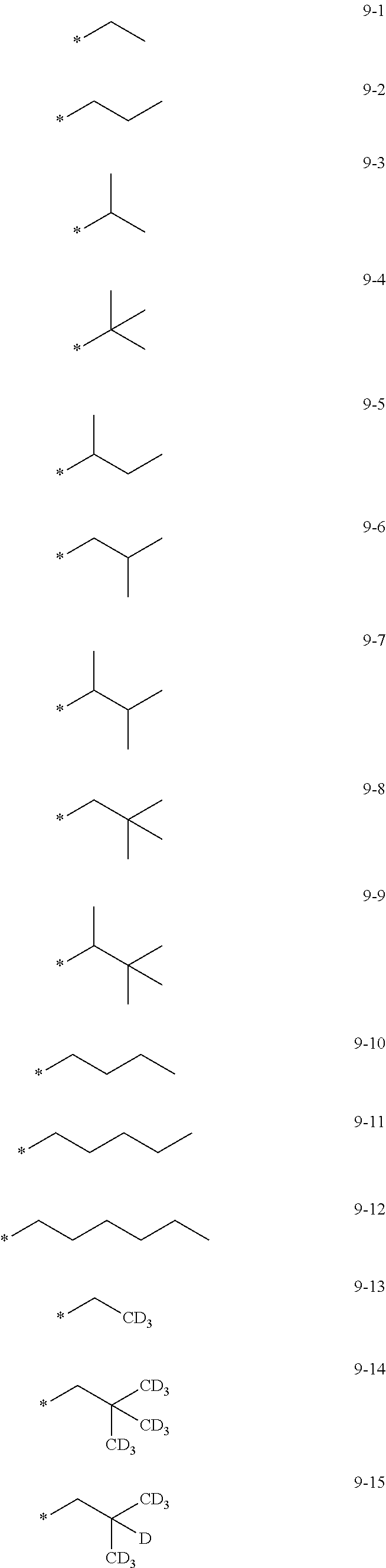
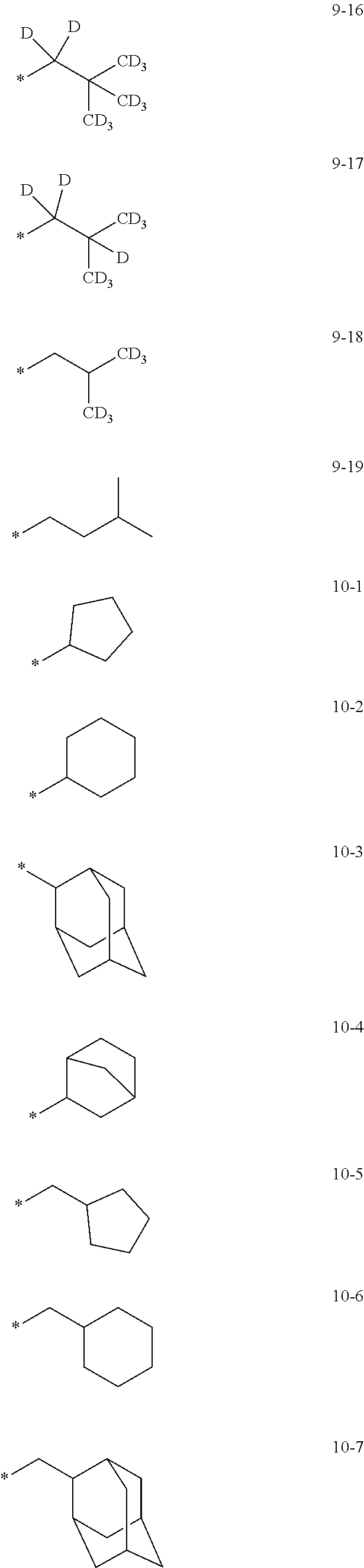
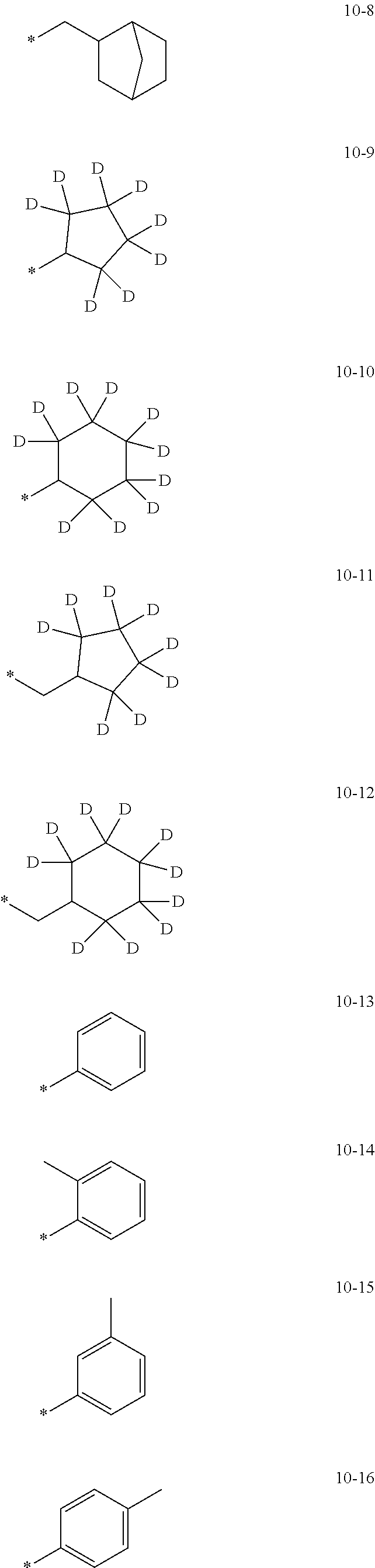


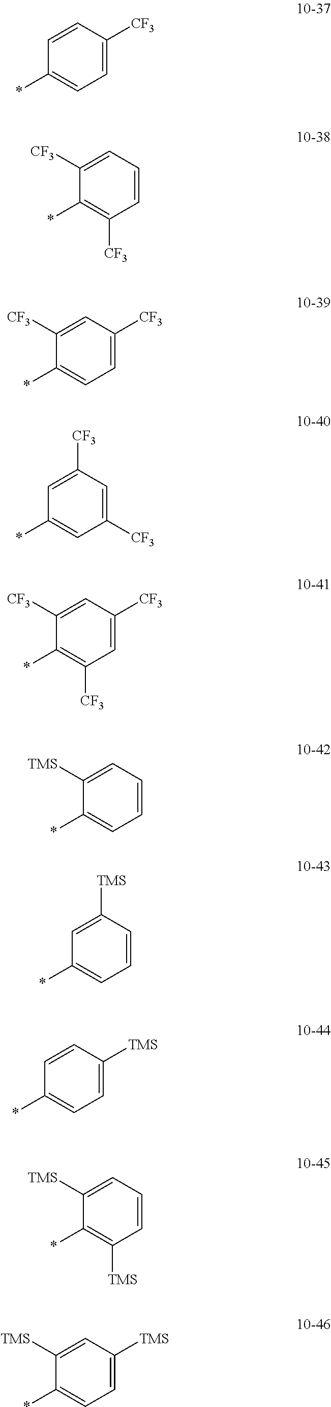


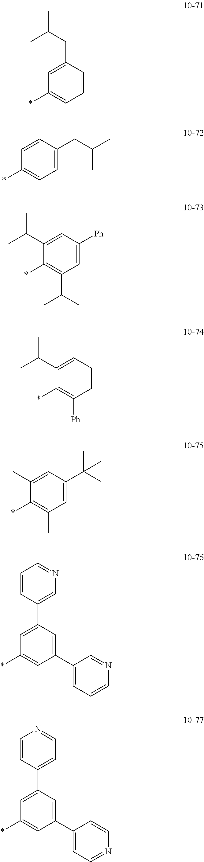


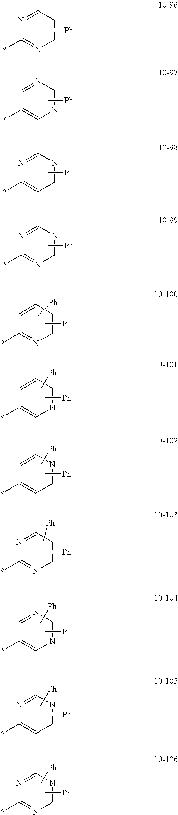


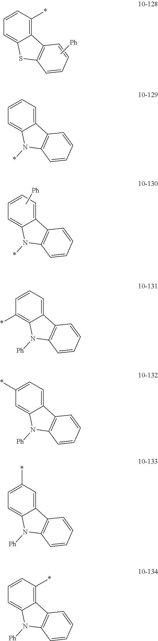
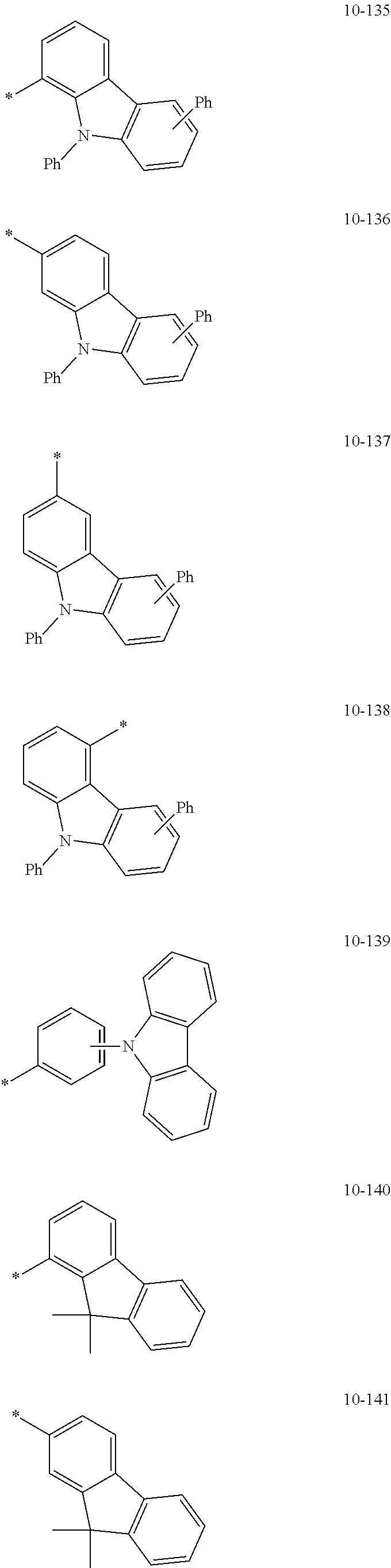


-

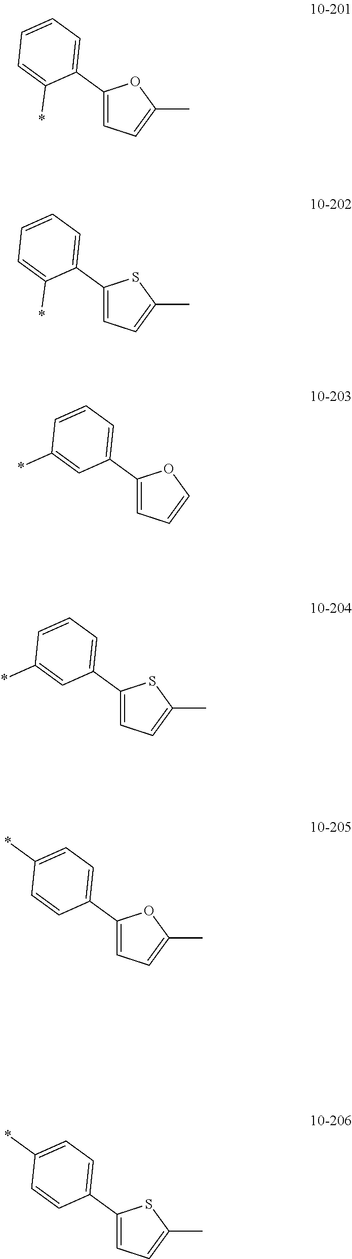
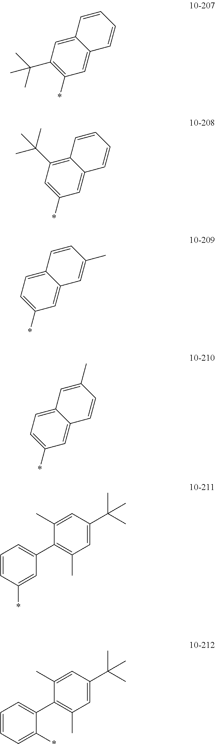

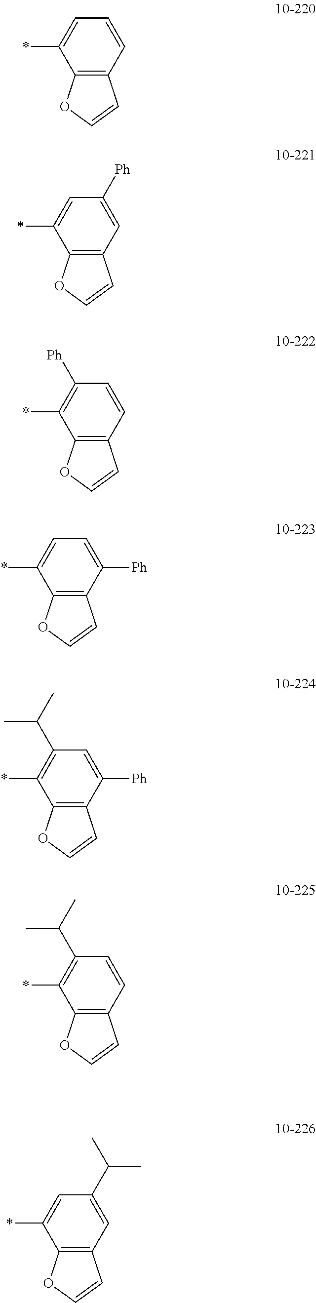
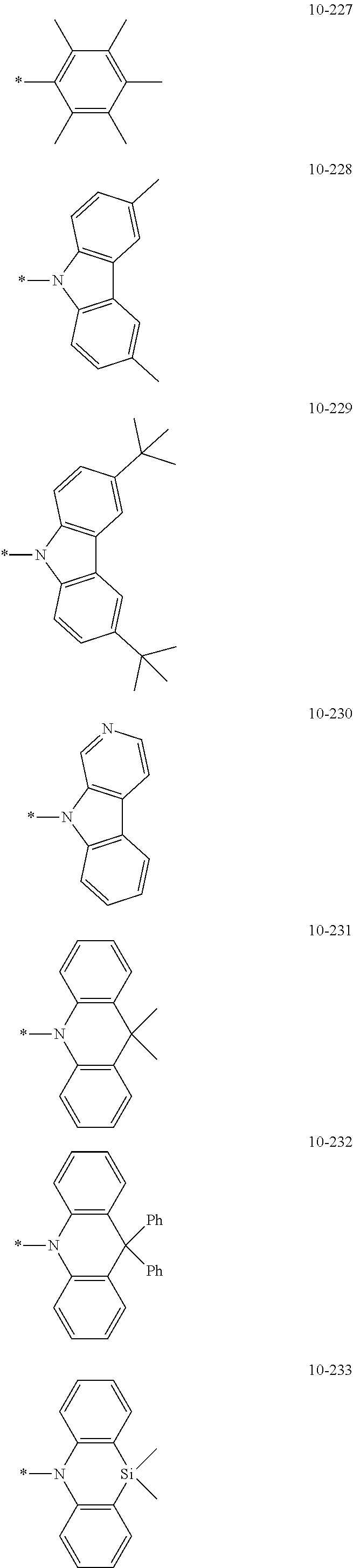


-
- wherein, in Formulae 9-1 to 9-19 and 10-1 to 10-246, * indicates a binding site to a neighboring atom, “D” represents a deuterium atom, “Ph” represents a phenyl group, and “TMS” represents a trimethylsilyl group.
- In Formulae 3-1 to 3-5, 502, and 503, a71 to a74 and a501 to a504 indicate the number of R71 to the number of R74 and the number of R501 to the number of R504, respectively, and may each independently be an integer from 0 to 20. When a71 is 2 or more, two or more of R71 may be identical to or different from each other, when a72 is 2 or more, two or more of R72 may be identical to or different from each other, when a73 is 2 or more, two or more of R73 may be identical to or different from each other, when a74 is 2 or more, two or more of R74 may be identical to or different from each other, when a501 is 2 or more, two or more of R501 may be identical to or different from each other, when a502 is 2 or more, two or more of R502 may be identical to or different from each other, when a503 is 2 or more, two or more of R503 may be identical to or different from each other, and when a504 is 2 or more, two or more of R504 may be identical to or different from each other. a71 to a74 and a501 to a504 may each independently be an integer from 0 to 8.
- Each of a group represented by *-(L51)b51-R51 and a group represented by *-(L52)b52-R52 in
Formula 2 may not be a phenyl group. - In one or more embodiments, a group represented by *-(L51)b51-R51 and a group represented by *-(L52)b52-R52 in
Formula 2 may be identical to each other. - In one or more embodiments, a group represented by *-(L51)b51-R51 and a group represented by *-(L52)b52-R52 in
Formula 2 may be different from each other. - In one or more embodiments, in
Formula 2, b51 and b52 may each be 1, 2, or 3, and L51 and L52 may each independently be a benzene group, a pyridine group, a pyrimidine group, a pyridazine group, a pyrazine group, or a triazine group, each unsubstituted or substituted with at least one R10a. - In one or more embodiments, R51 and R52 in
Formula 2 may each independently be a C3-C60 carbocyclic group that is unsubstituted or substituted with at least one R10a, a C1-C60 heterocyclic group that is unsubstituted or substituted with at least one R10a, a C6-C60 aryloxy group that is unsubstituted or substituted with at least one R10a, a C6-C60 arylthio group that is unsubstituted or substituted with at least one R10a, —C(Q1)(Q2)(Q3), or —Si(Q1)(Q2)(Q3), and -
- Q1 to Q3 may each independently be a C3-C60 carbocyclic group or a C1-C60 heterocyclic group, each unsubstituted or substituted with deuterium, —F, a cyano group, a C1-C60 alkyl group, a C1-C60 alkoxy group, a phenyl group, a biphenyl group, or a (e.g., any) combination thereof.
- In one or more embodiments,
-
- a group represented by *-(L51)b51-R51 in
Formula 2 may be a group represented by one of Formulae CY51-1 to CY51-26, and/or - a group represented by *-(L52)b52-R52 in
Formula 2 may be a group represented by one of Formulae CY52-1 to CY52-26, and/or - a group represented by *-(L53)b53-R53 in
Formula 2 may be a group represented by one of Formulae CY53-1 to CY53-27, —C(Q1)(Q2)(Q3), or —Si(Q1)(Q2)(Q3) (Q1 to Q3 may be the same as described herein):
- a group represented by *-(L51)b51-R51 in
-


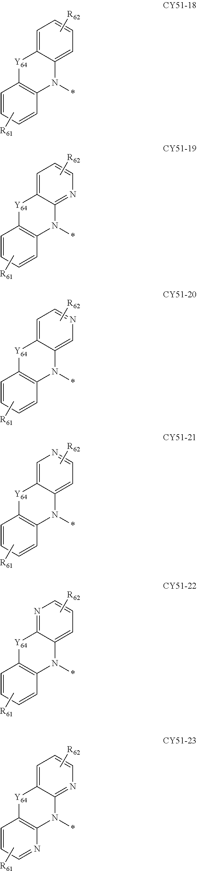
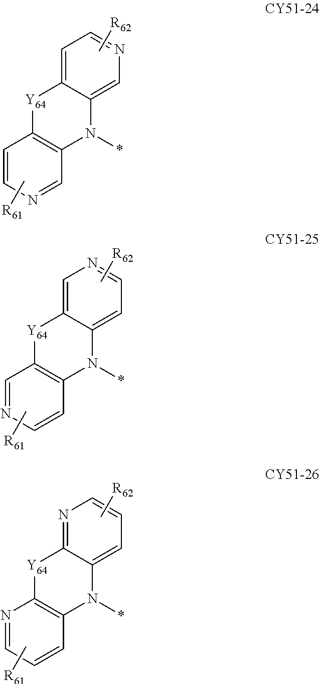
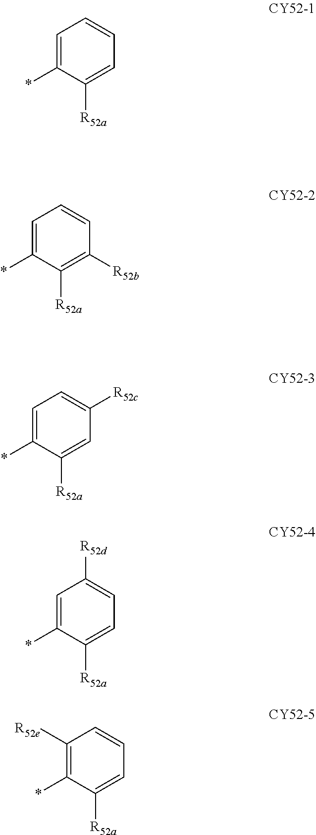


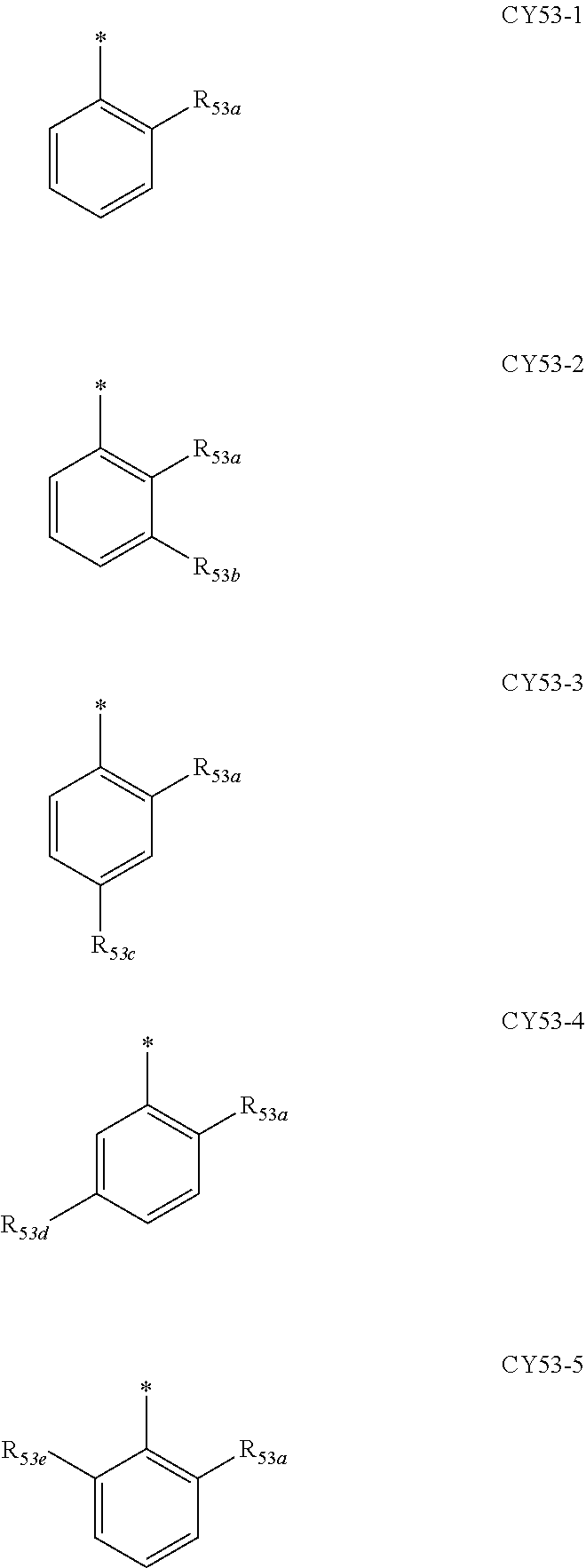

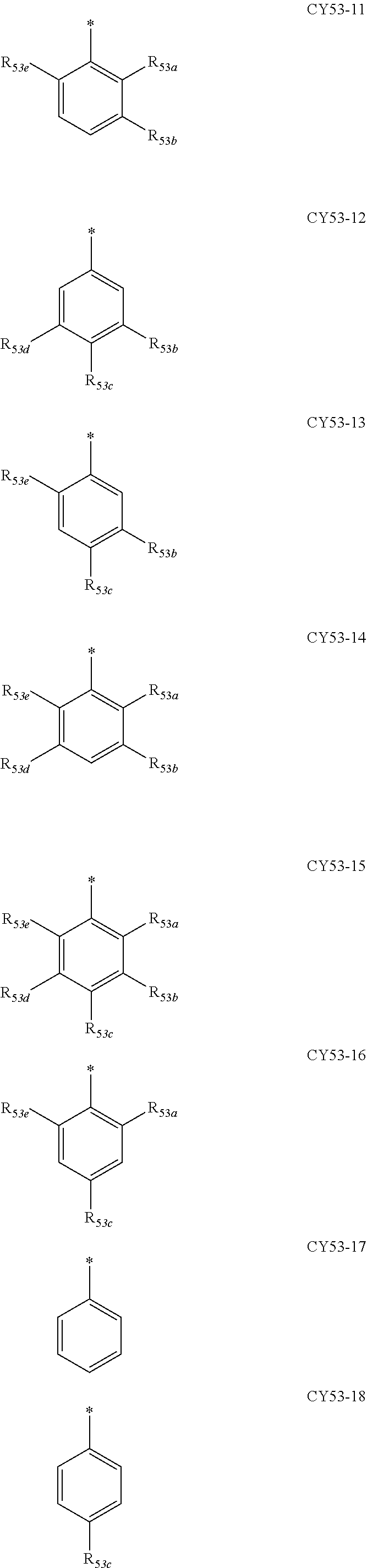

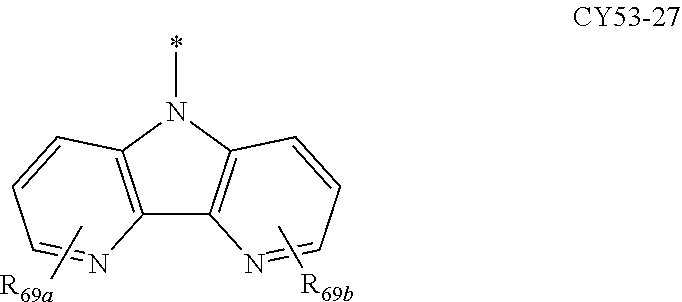
-
- wherein, in Formulae CY51-1 to CY51-26, CY52-1 to CY52-26, and CY53-1 to CY53-27,
- Y63 may be a single bond, O, S, N(R63), B(R63), C(R363a)(R363b), or Si(R63a)(R63b),
- Y64 may be a single bond, O, S, N(R64), B(R64), C(R64a)(R64b), or Si(R64a)(R64b),
- Y67 may be a single bond, O, S, N(R67), B(R67), C(R67a)(R67b), or Si(R67a)(R67b),
- Y68 may be a single bond, O, S, N(R68), B(R68), C(R68a)(R68b), or Si(R68a)(R68b),
- each of Y63 and Y64 in Formulae CY51-16 and CY51-17 may not be a single bond simultaneously (e.g., at the same time),
- each of Y67 and Y68 in Formulae CY52-16 and CY52-17 may not be a single bond simultaneously (e.g., at the same time),
- R51a to R51e, R61 to R64, R63a, R63b, R64a, and R64b are each as described in connection with R51, wherein R51a to R51e may not each be hydrogen,
- R52a to R52e, R65 to R68, R67a, R67b, R68a, and R68b are each as described in connection with R52, wherein R52a to R52e may not each be hydrogen,
- R53a to R53e, R69a, and R69b are each as described in connection with R53, and R53a to R53e may not each be hydrogen, and
- * indicates a binding site to a neighboring atom.
- In one or more embodiments,
-
- R51a to R51e and R52a to R52e in Formulae CY51-1 to CY51-26 and Formulae CY52-1 to CY52-26 may each independently be:
- a cyclopentyl group, a cyclohexyl group, a cycloheptyl group, a cyclooctyl group, an adamantanyl group, a norbornanyl group, a norbornenyl group, a cyclopentenyl group, a cyclohexenyl group, a cycloheptenyl group, a phenyl group, a biphenyl group, a C1-C10 alkylphenyl group, a naphthyl group, a fluorenyl group, a phenanthrenyl group, an anthracenyl group, a fluoranthenyl group, a triphenylenyl group, a pyrenyl group, a chrysenyl group, a pyrrolyl group, a thiophenyl group, a furanyl group, an imidazolyl group, a pyrazolyl group, a thiazolyl group, an isothiazolyl group, an oxazolyl group, an isoxazolyl group, a pyridinyl group, a pyrazinyl group, a pyrimidinyl group, a pyridazinyl group, an isoindolyl group, an indolyl group, an indazolyl group, a purinyl group, a quinolinyl group, an isoquinolinyl group, a benzoquinolinyl group, a quinoxalinyl group, a quinazolinyl group, a cinnolinyl group, a carbazolyl group, a phenanthrolinyl group, a benzoimidazolyl group, a benzofuranyl group, a benzothiophenyl group, a benzoisothiazolyl group, a benzoxazolyl group, a benzoisoxazolyl group, a triazolyl group, a tetrazolyl group, an oxadiazolyl group, a triazinyl group, a dibenzofuranyl group, a dibenzothiophenyl group, a benzocarbazolyl group, a dibenzocarbazolyl group, an imidazopyridinyl group, an imidazopyrimidinyl group, an azacarbazolyl group, an azadibenzofuranyl group, an azadibenzothiophenyl group, an azafluorenyl group, an azadibenzosilolyl group, or a group represented by Formula 91, each unsubstituted or substituted with deuterium, —F, —Cl, —Br, —I, —CD3, —CD2H, —CDH2, —CF3, —CF2H, —CFH2, a hydroxyl group, a cyano group, a nitro group, a C1-C20 alkyl group, a C1-C20 alkoxy group, a cyclopentyl group, a cyclohexyl group, a cycloheptyl group, a cyclooctyl group, an adamantanyl group, a norbornanyl group, a norbornenyl group, a cyclopentenyl group, a cyclohexenyl group, a cycloheptenyl group, a phenyl group, a biphenyl group, a C1-C10 alkylphenyl group, a naphthyl group, a fluorenyl group, a phenanthrenyl group, an anthracenyl group, a fluoranthenyl group, a triphenylenyl group, a pyrenyl group, a chrysenyl group, a pyrrolyl group, a thiophenyl group, a furanyl group, an imidazolyl group, a pyrazolyl group, a thiazolyl group, an isothiazolyl group, an oxazolyl group, an isoxazolyl group, a pyridinyl group, a pyrazinyl group, a pyrimidinyl group, a pyridazinyl group, an isoindolyl group, an indolyl group, an indazolyl group, a purinyl group, a quinolinyl group, an isoquinolinyl group, a benzoquinolinyl group, a quinoxalinyl group, a quinazolinyl group, a cinnolinyl group, a carbazolyl group, a phenanthrolinyl group, a benzoimidazolyl group, a benzofuranyl group, a benzothiophenyl group, a benzoisothiazolyl group, a benzoxazolyl group, a benzoisoxazolyl group, a triazolyl group, a tetrazolyl group, an oxadiazolyl group, a triazinyl group, a dibenzofuranyl group, a dibenzothiophenyl group, a benzocarbazolyl group, a dibenzocarbazolyl group, an imidazopyridinyl group, an imidazopyrimidinyl group, or a (e.g., any) combination thereof; or
- —C(Q1)(Q2)(Q3) or —Si(Q1)(Q2)(Q3), and
- Q1 to Q3 may each independently be a phenyl group, a naphthyl group, a pyridinyl group, a pyrimidinyl group, a pyridazinyl group, a pyrazinyl group, or a triazinyl group, each unsubstituted or substituted with deuterium, a C1-C10 alkyl group, a phenyl group, a biphenyl group, a pyridinyl group, a pyrimidinyl group, a pyridazinyl group, a pyrazinyl group, a triazinyl group, or a (e.g., any) combination thereof,
- in Formulae CY51-16 and CY51-17, i) Y63 may be O or S, and Y64 may be Si(R64a)(R64b), or ii) Yes may be Si(R63a)(R63b), and Y64 may be O or S, and
- in Formulae CY52-16 and CY52-17, i) Y67 may be O or S, and Yes may be Si(R68a)(R68b), or ii) Y67 may be Si(R67a)(R67b), and Yes may be O or S.
- In Formulae 3-1 to 3-5, L81 to L85 may each independently be:
-
- a single bond; or
- *—C(Q4)(Q5)-*′ or *—Si(Q4)(Q5)-*′, * and *′ each indicate a binding site to a neighboring atom; or
- a benzene group, a naphthalene group, an anthracene group, a phenanthrene group, a triphenylene group, a pyrene group, a chrysene group, a cyclopentadiene group, a furan group, a thiophene group, a silole group, an indene group, a fluorene group, an indole group, a carbazole group, a benzofuran group, a dibenzofuran group, a benzothiophene group, a dibenzothiophene group, a benzosilole group, a dibenzosilole group, an azafluorene group, an azacarbazole group, an azadibenzofuran group, an azadibenzothiophene group, an azadibenzosilole group, a pyridine group, a pyrimidine group, a pyrazine group, a pyridazine group, a triazine group, a quinoline group, an isoquinoline group, a quinoxaline group, a quinazoline group, a phenanthroline group, a pyrrole group, a pyrazole group, an imidazole group, a triazole group, an oxazole group, an isoxazole group, a thiazole group, an isothiazole group, an oxadiazole group, a thiadiazole group, a benzopyrazole group, a benzimidazole group, a benzoxazole group, a benzothiazole group, a benzoxadiazole group, or a benzothiadiazole group, each unsubstituted or substituted with deuterium, —F, —Cl, —Br, —I, a hydroxyl group, a cyano group, a nitro group, a C1-C20 alkyl group, a C1-C20 alkoxy group, a phenyl group, a naphthyl group, a pyridinyl group, a pyrimidinyl group, a triazinyl group, a fluorenyl group, a dimethylfluorenyl group, a diphenylfluorenyl group, a carbazolyl group, a phenylcarbazolyl group, a dibenzofuranyl group, a dibenzothiophenyl group, a dibenzosilolyl group, a dimethyldibenzosilolyl group, a diphenyldibenzosilolyl group, —O(Q31), —S(Q31), —Si(Q31)(Q32)(Q33), —N(Q31)(Q32), —B(Q31)(Q32), —P(Q31)(Q32), —C(═O)(Q31), —S(═O)2(Q31), —P(═O)(Q31)(Q32), or a (e.g., any) combination thereof, and
- Q4, Q5, and Q31 to Q33 may each independently be hydrogen, deuterium, a C1-C20 alkyl group, a C1-C20 alkoxy group, a phenyl group, a biphenyl group, a terphenyl group, a pyridinyl group, a pyrimidinyl group, a pyridazinyl group, a pyrazinyl group, or a triazinyl group.
- In one or more embodiments, a group represented by
-
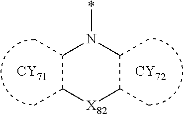
- in Formulae 3-1 and 3-2 may be a group represented by one of Formulae CY71-1(1) to CY71-1(8), and/or
-
- a group represented by
-
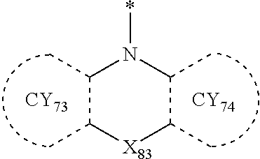
-
- in Formulae 3-1 and 3-3 may be a group represented by one of Formulae CY71-2(1) to CY71-2(8), and/or
- a group represented by
-

-
- in Formulae 3-2 and 3-4 may be a group represented by one of Formulae CY71-3(1) to CY71-3(32), and/or
- a group represented by
-

-
- in Formulae 3-3 to 3-5 may be a group represented by one of Formulae CY71-4(1) to CY71-4(32), and/or
- a group represented by
-

-
- in Formula 3-5 may be a group represented by one of Formulae CY71-5(1) to CY71-5(8):
-

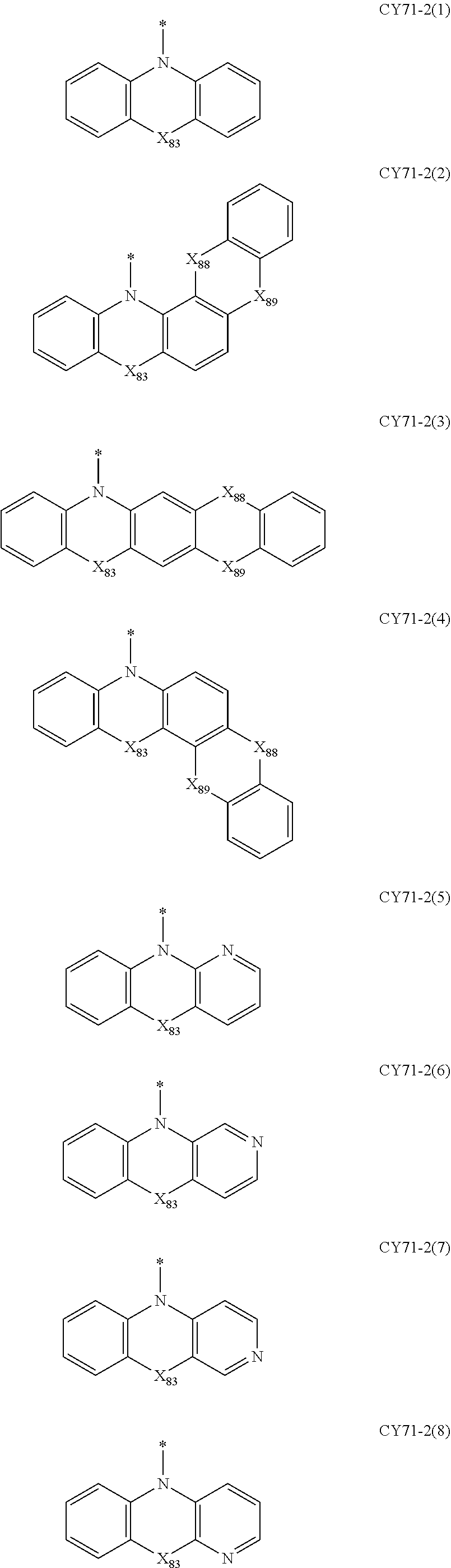

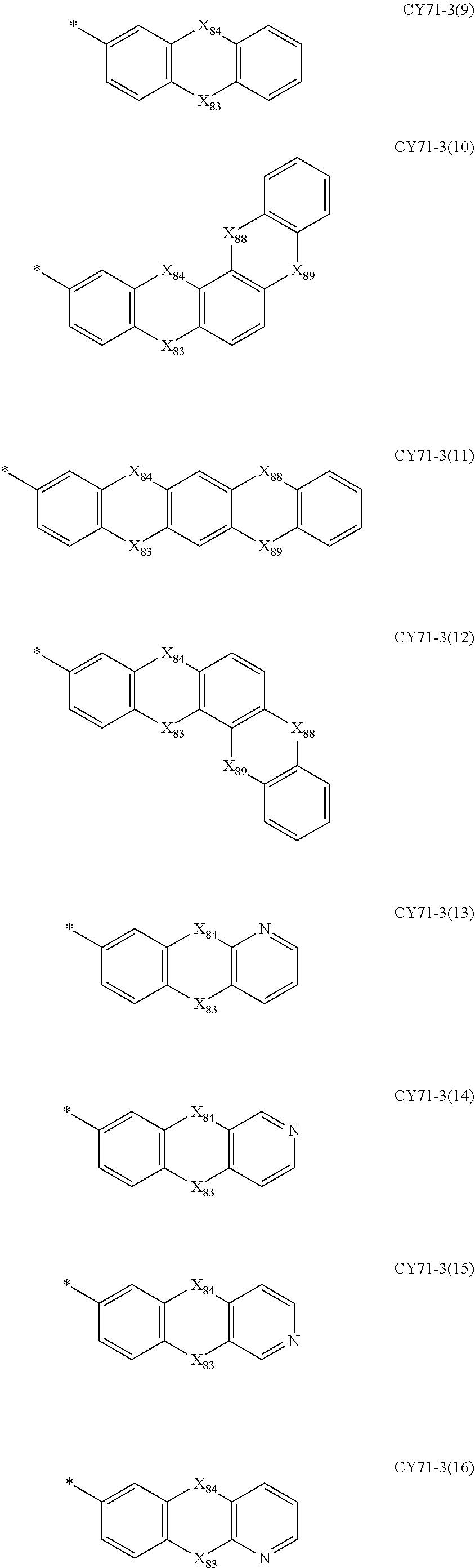

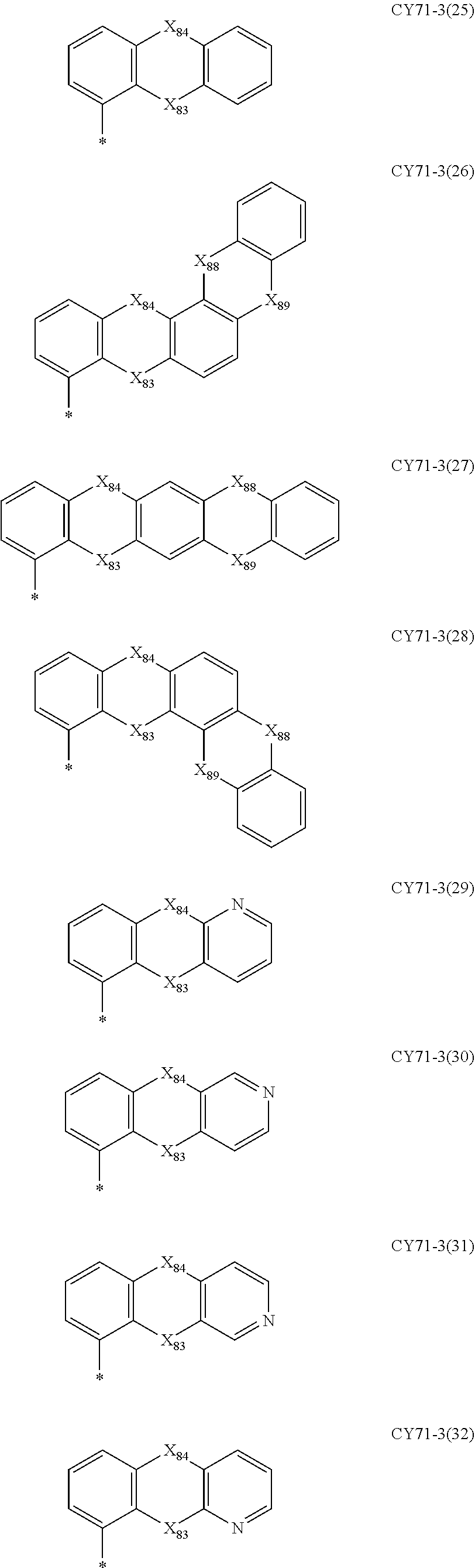
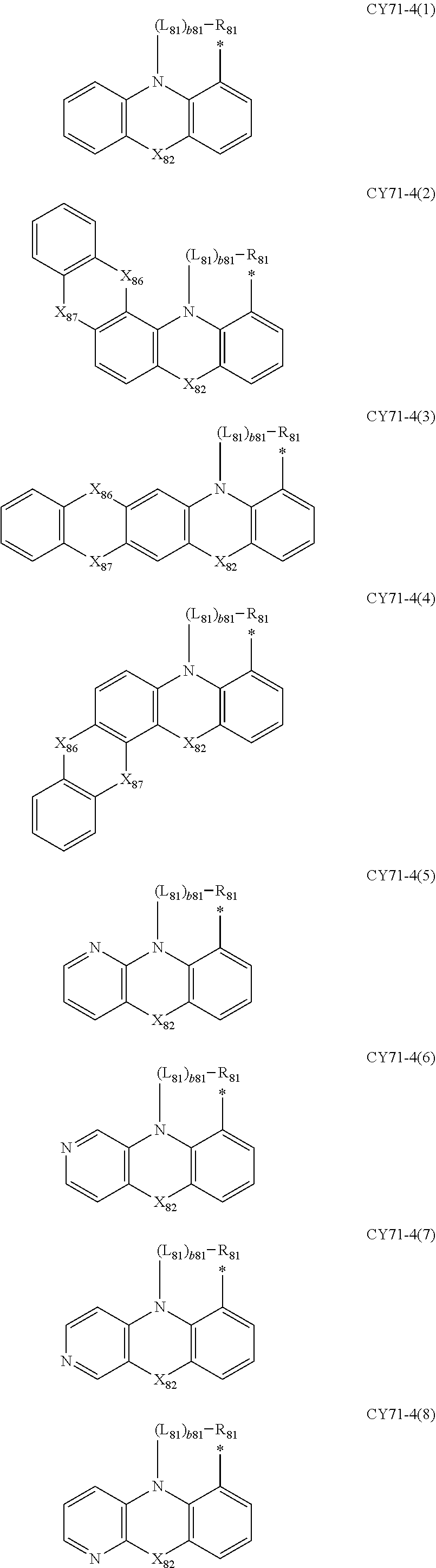

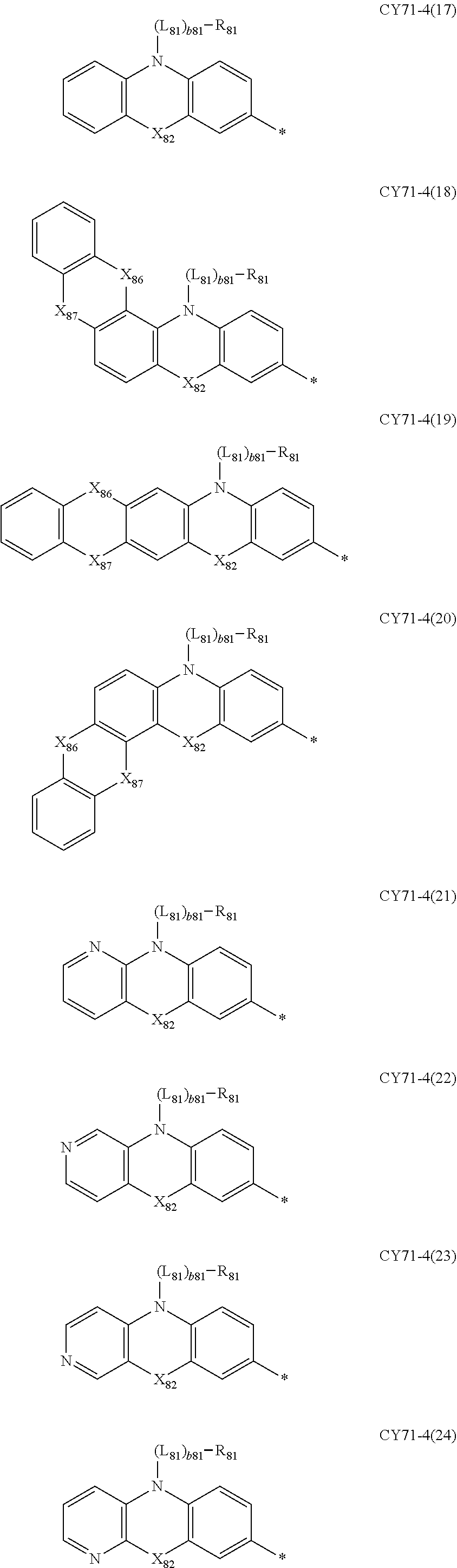


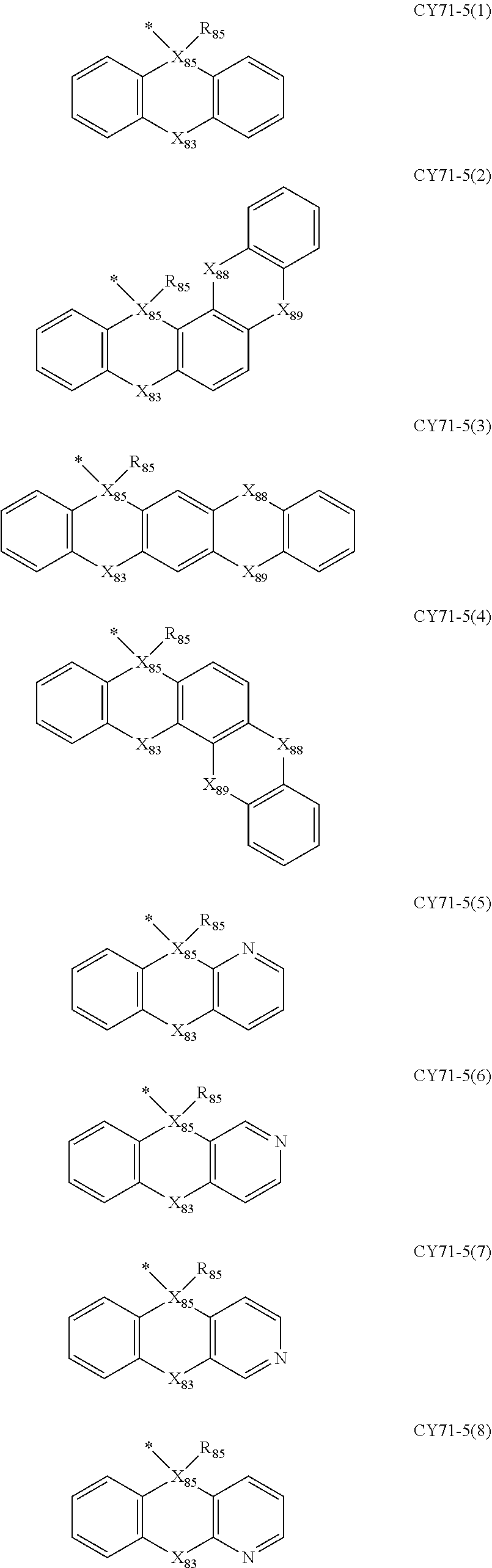
-
- wherein, in Formulae CY71-1(1) to CY71-1(8), CY71-2(1) to CY71-2(8), CY71-3(1) to CY71-3(32), CY71-4(1) to CY71-4(32), and CY71-5(1) to CY71-5(8),
- X81 to X85, L81, b81, R81, and R85 are each as described herein,
- X86 may be a single bond, O, S, N(R86), B(R86), C(R86a)(R86b), or Si(R86a)(R86b),
- X87 may be a single bond, O, S, N(R87), B(R87), C(R87a)(R87b), or Si(R87a)(R87b),
- in Formulae CY71-1(1) to CY71-1(8) and CY71-4(1) to CY71-4(32), each of X86 and X87 may not be a single bond at the same time,
- X88 may be a single bond, O, S, N(R88), B(R88), C(R88a)(R88b), or Si(R88a)(R88b),
- X89 may be a single bond, O, S, N(R89), B(R89), C(R89a)(R89b), or Si(R89a)(R89b),
- in Formulae CY71-2(1) to CY71-2(8), CY71-3(1) to CY71-3(32), and CY71-5(1) to CY71-5(8), each of X88 and X89 may not be a single bond at the same time, and
- R86 to R89, R86a, R86b, R87a, R87b, R88a, R88b, R89a, and R89b are each as described in connection with R81.
- In one or more embodiments, the organometallic compound represented by Formula 1 may be at least one of Compounds 1 to 344:
-


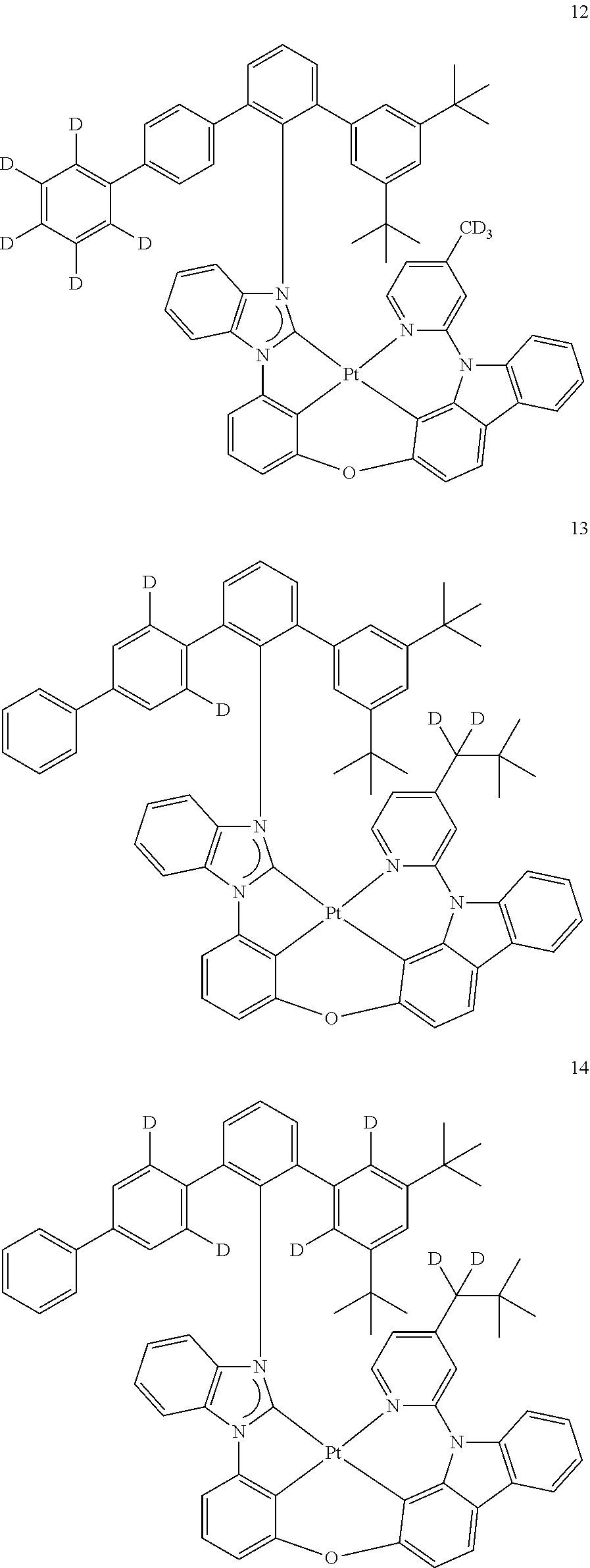
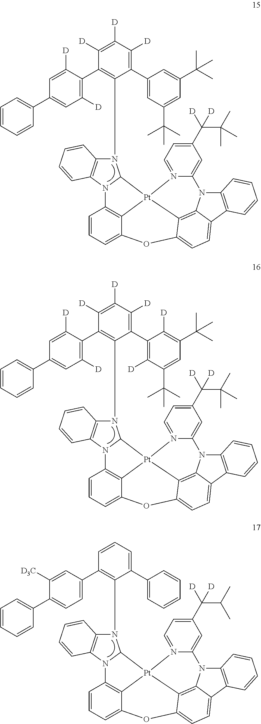
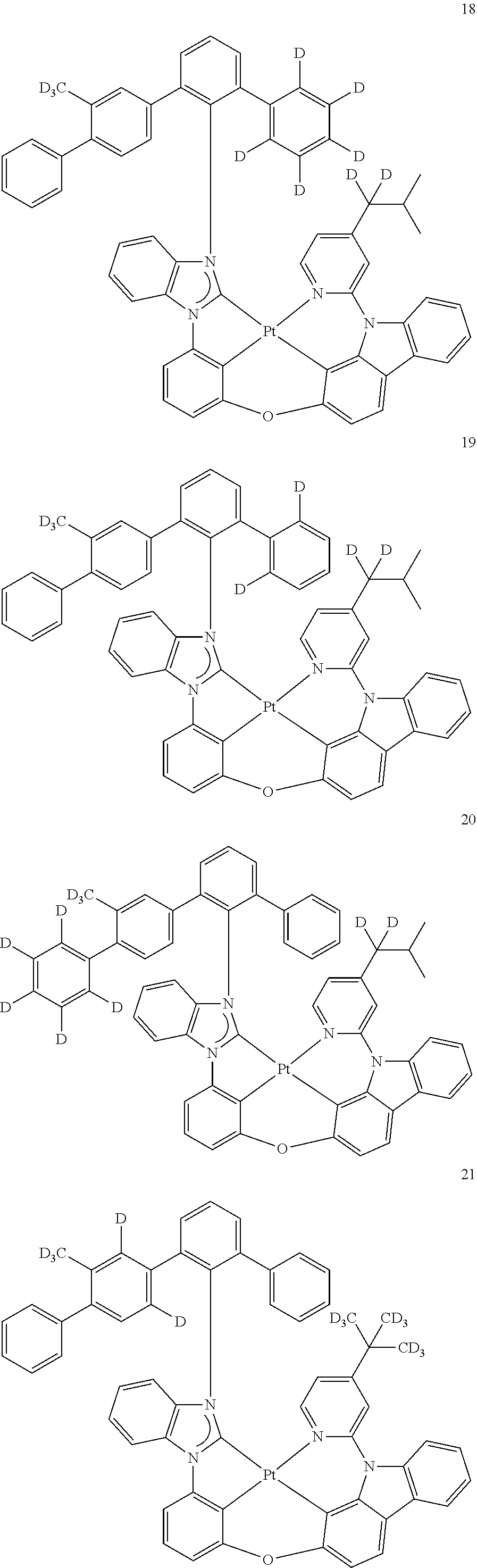
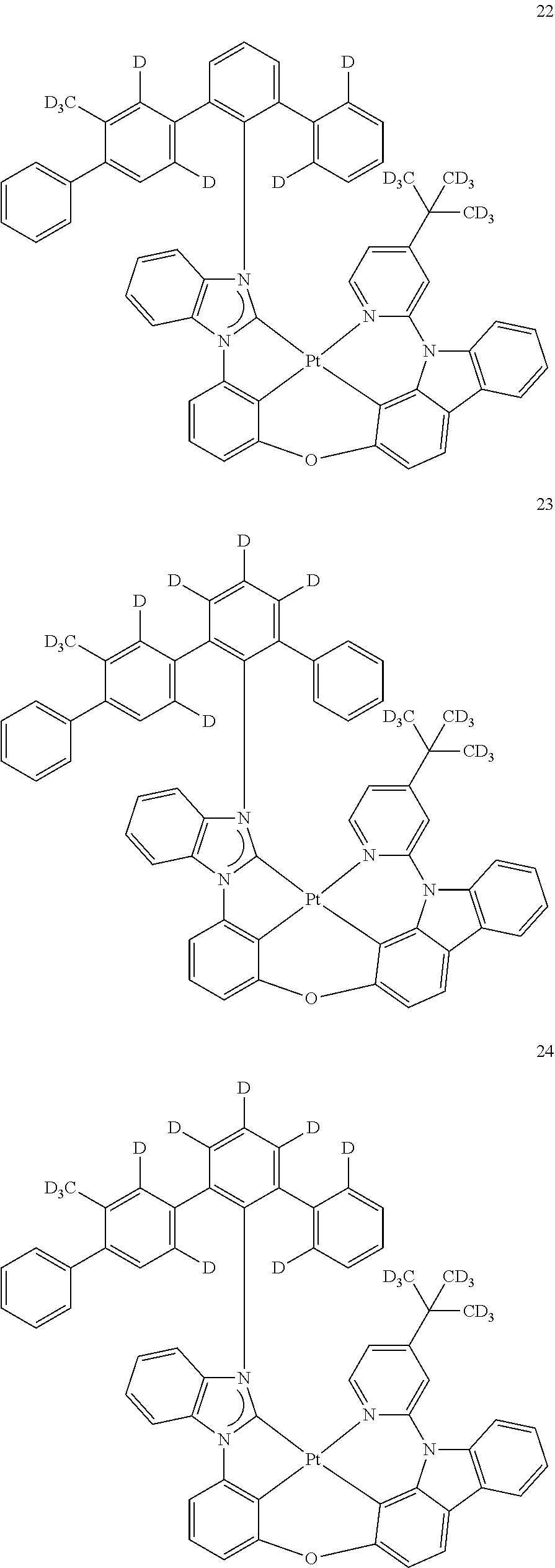
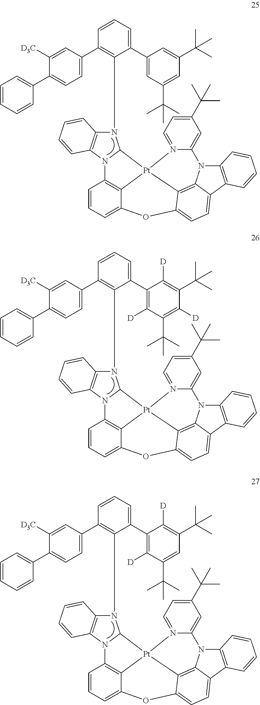

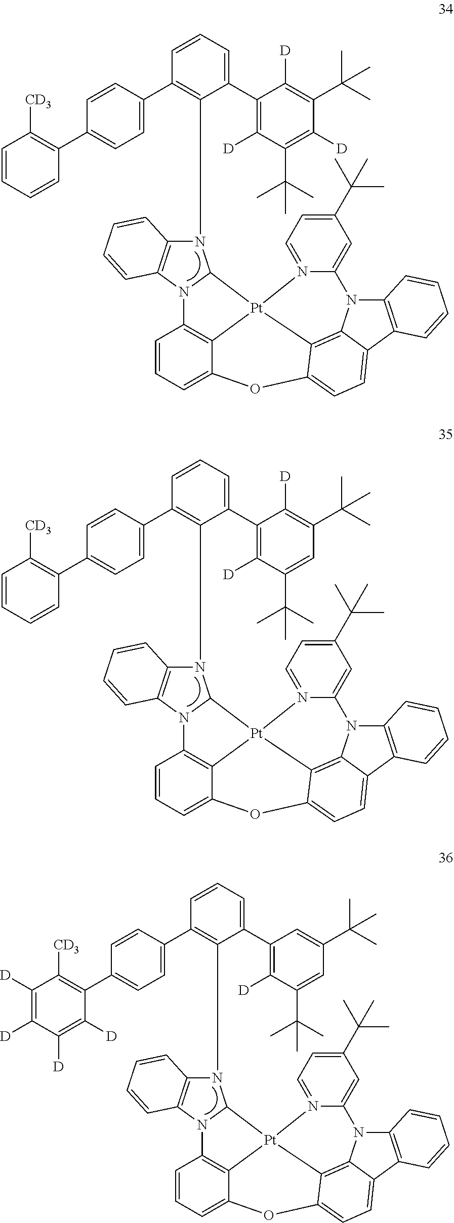
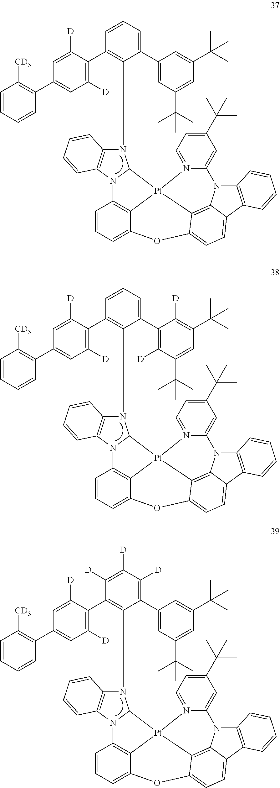


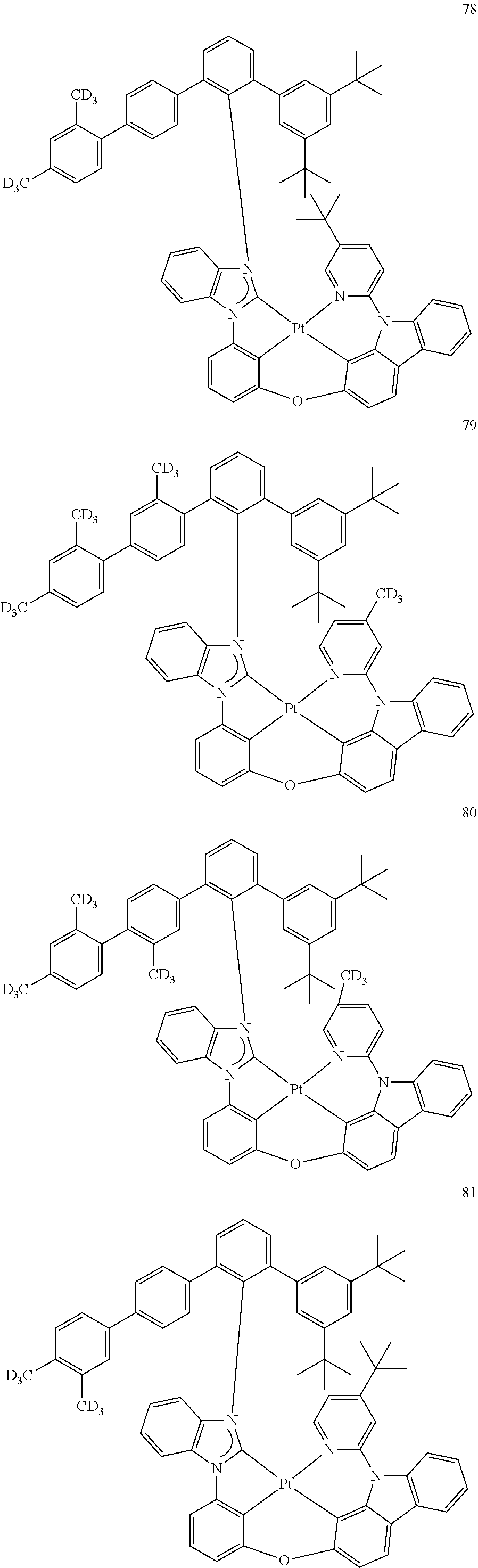
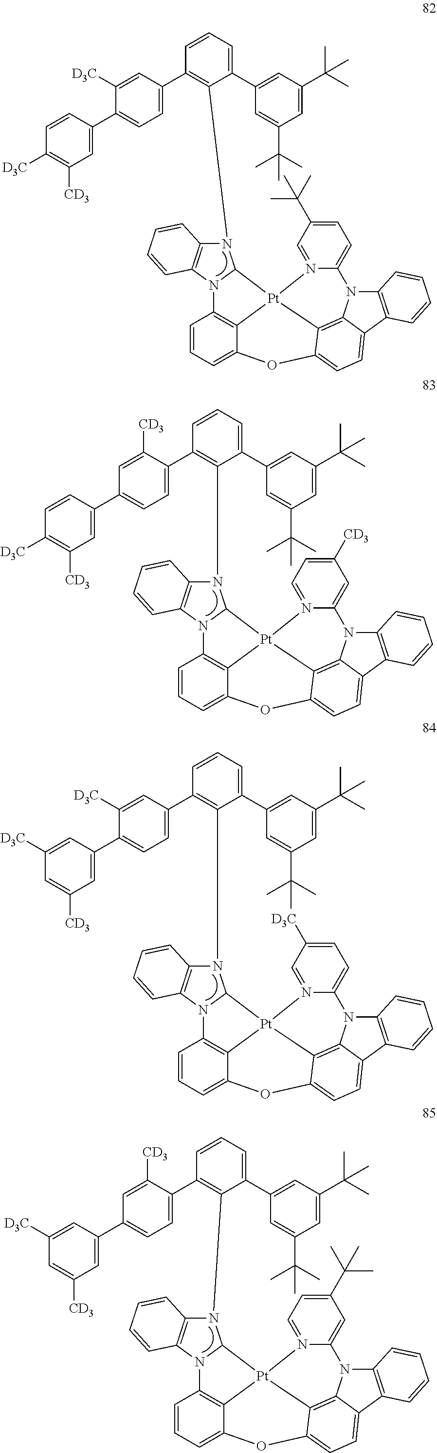
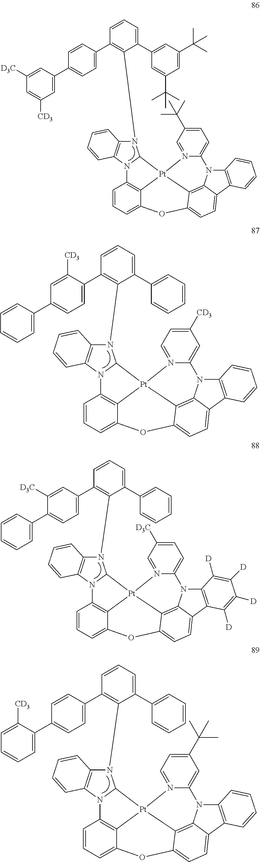
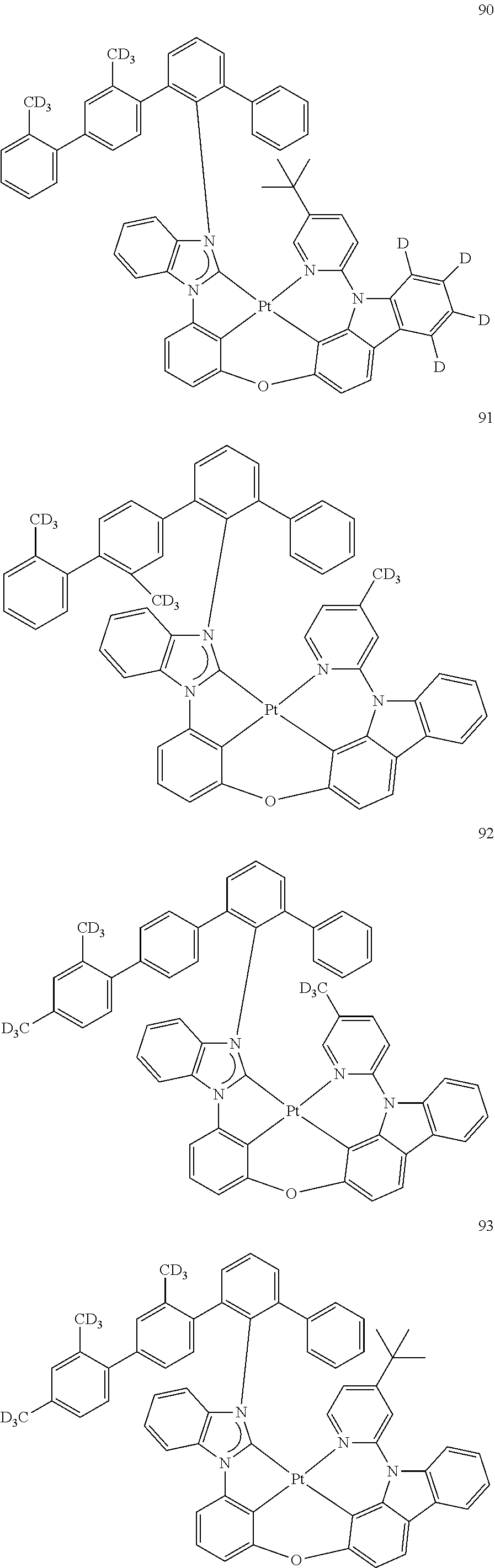
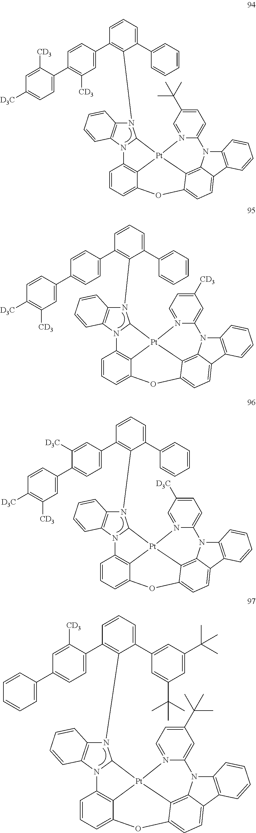
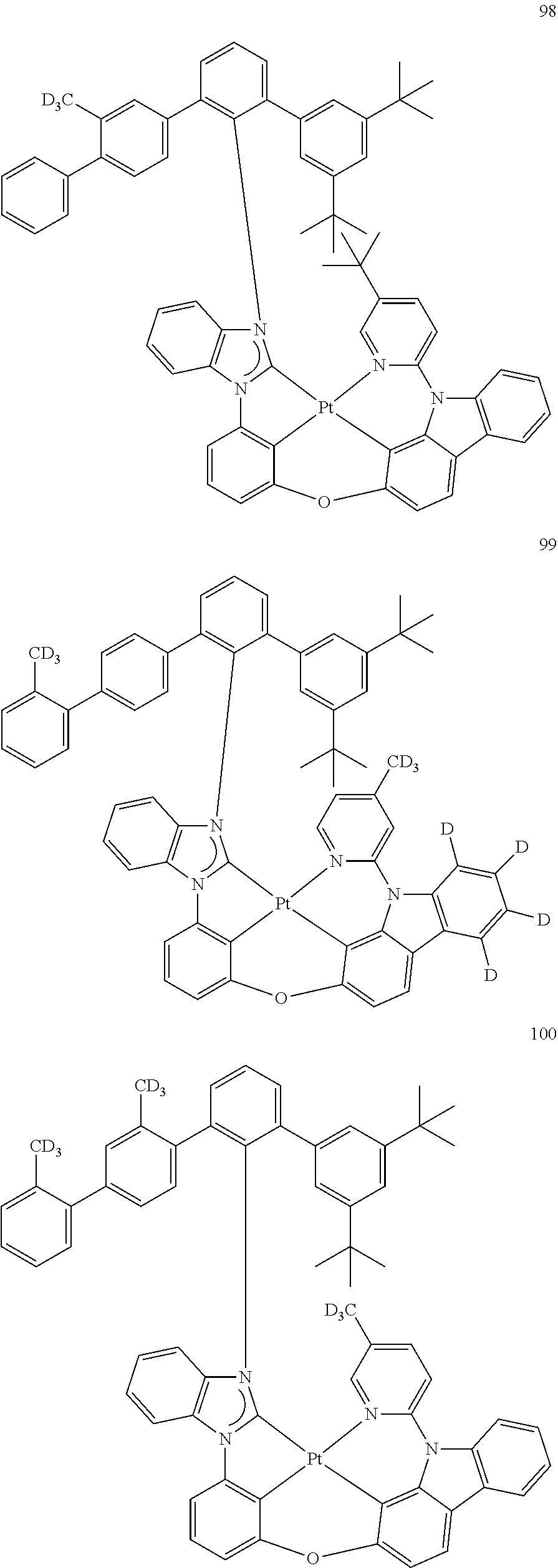
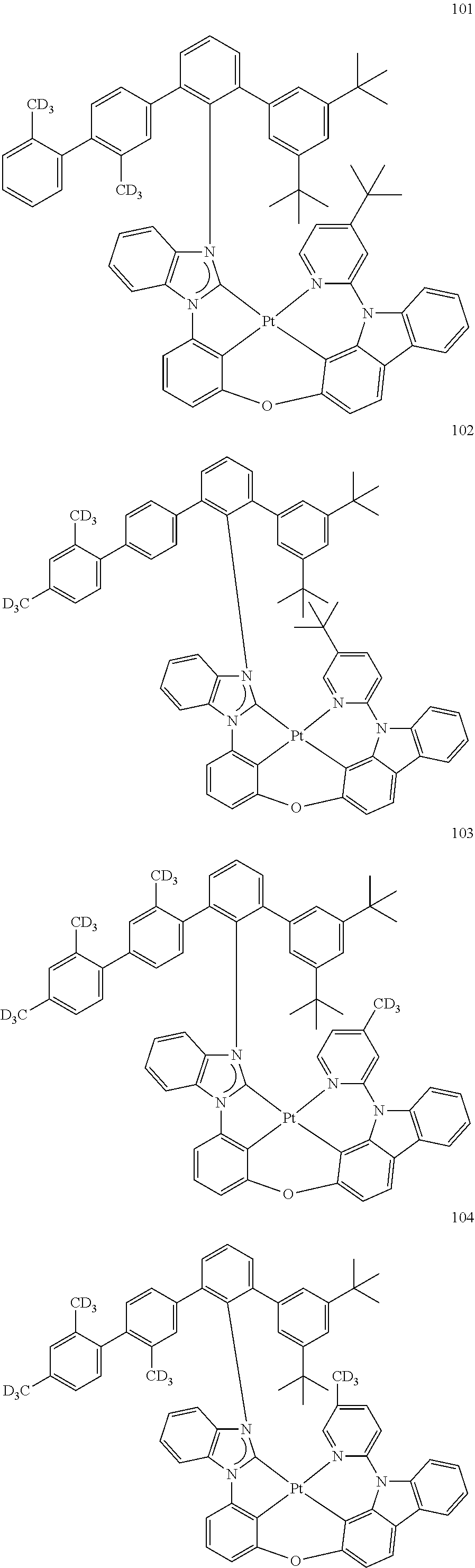
-


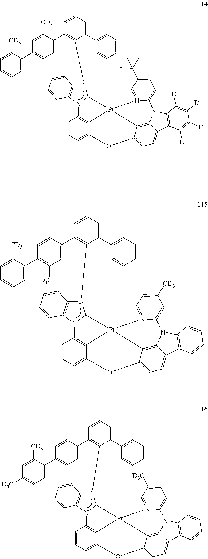
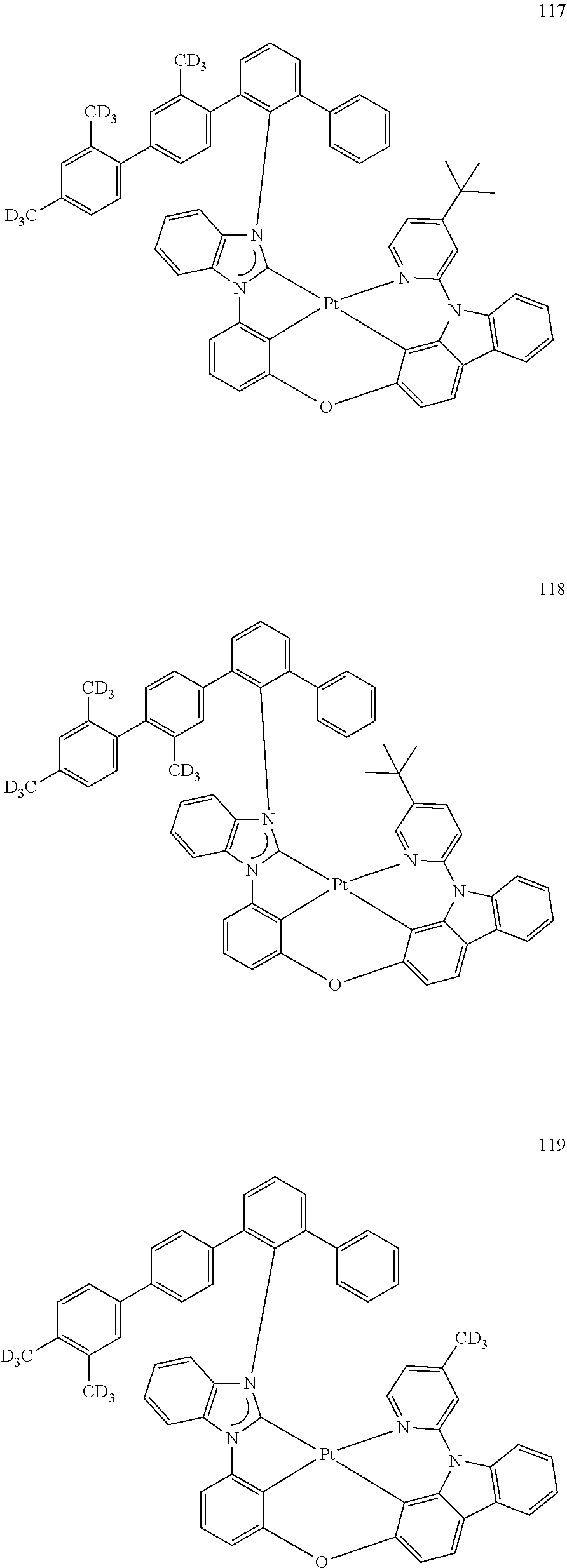
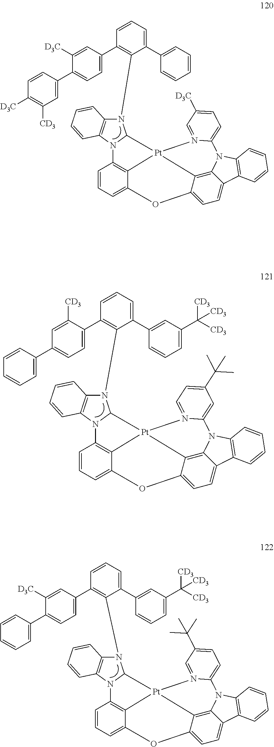
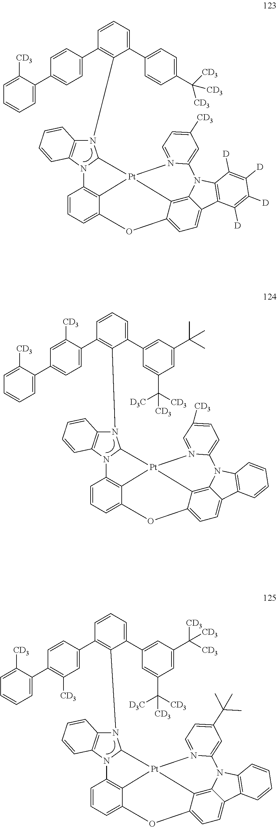


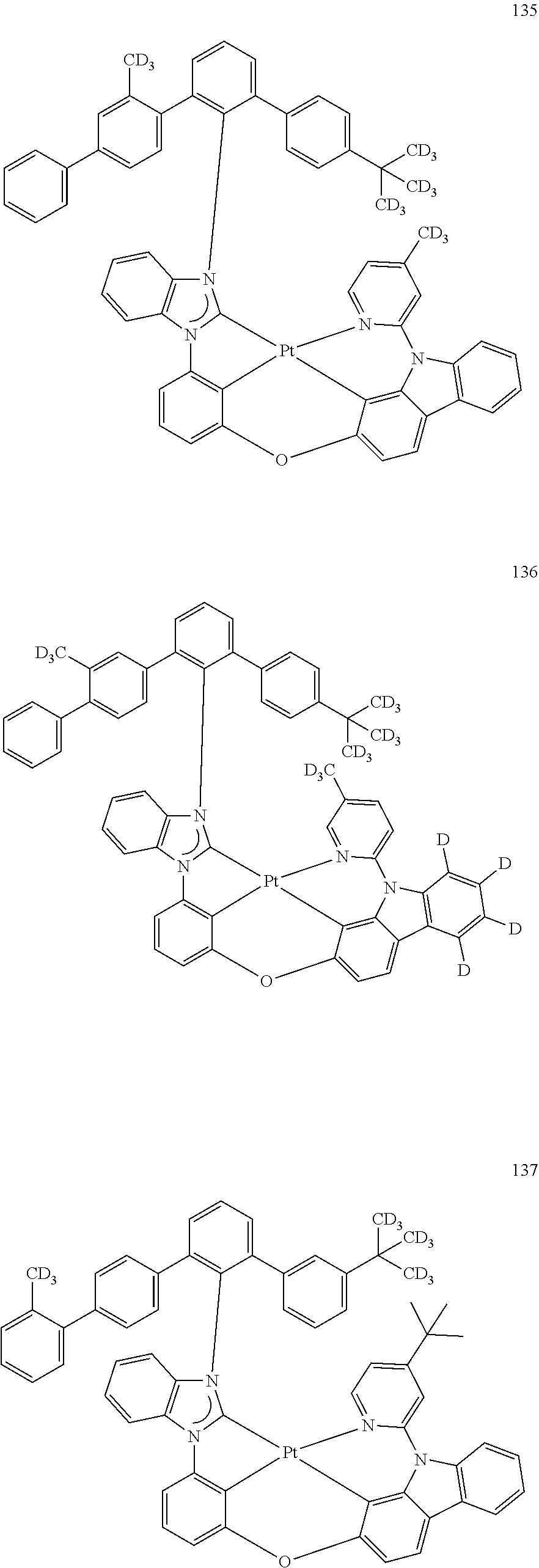

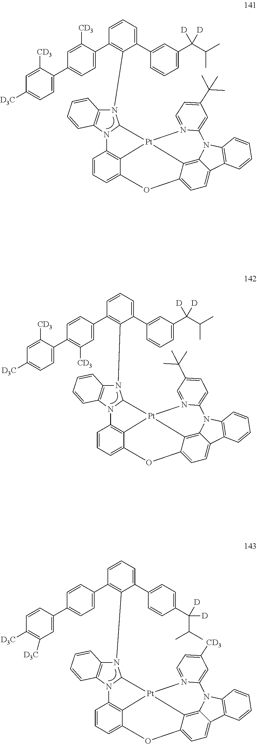
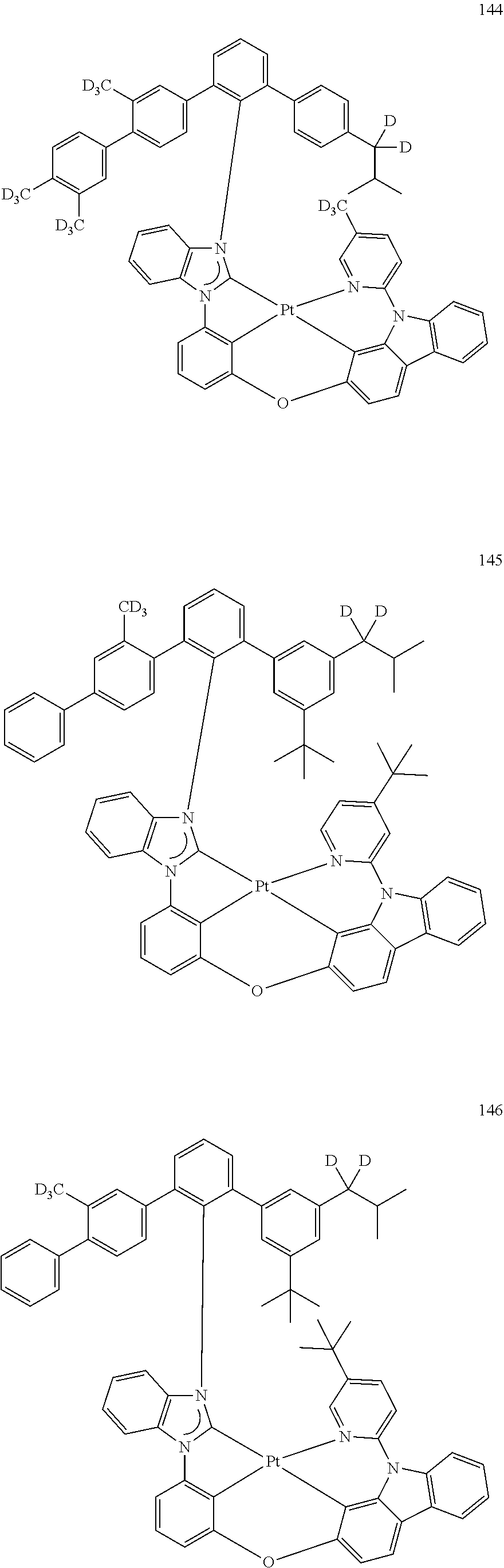
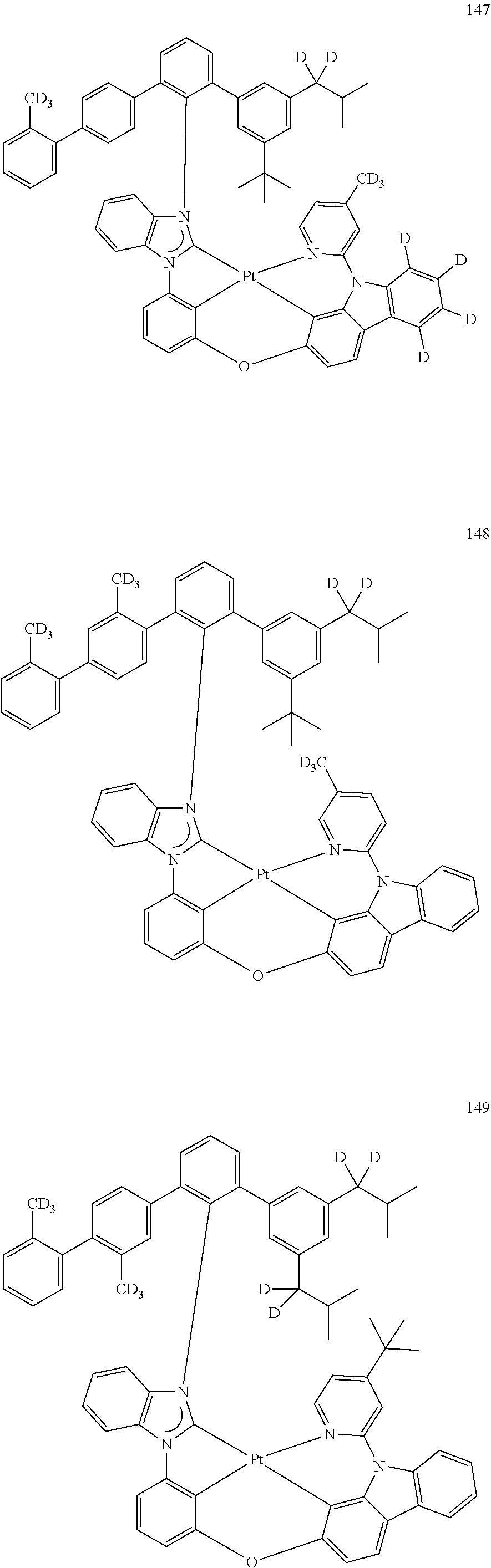

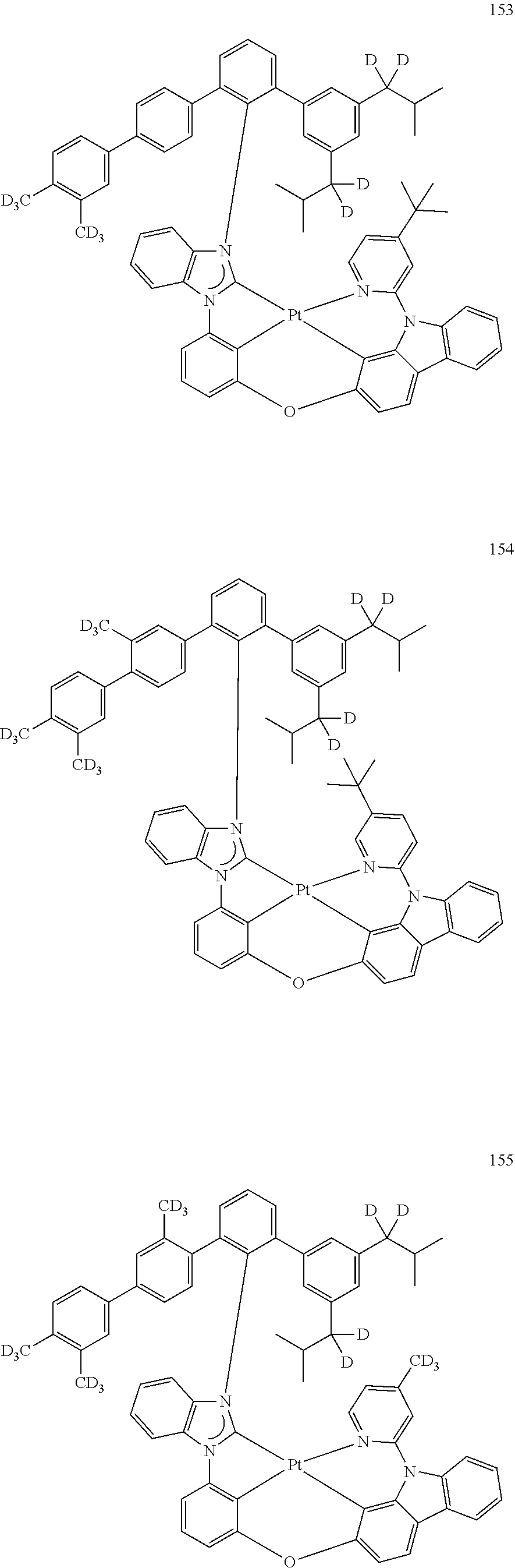


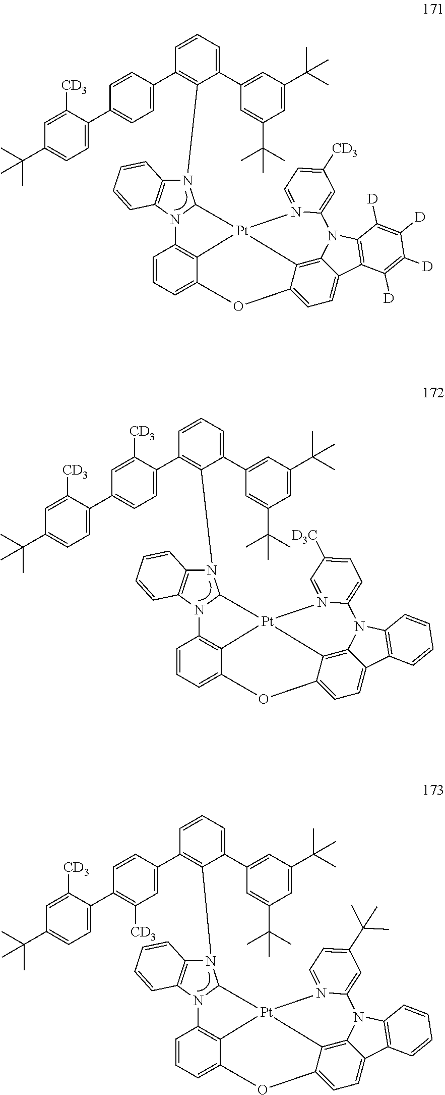
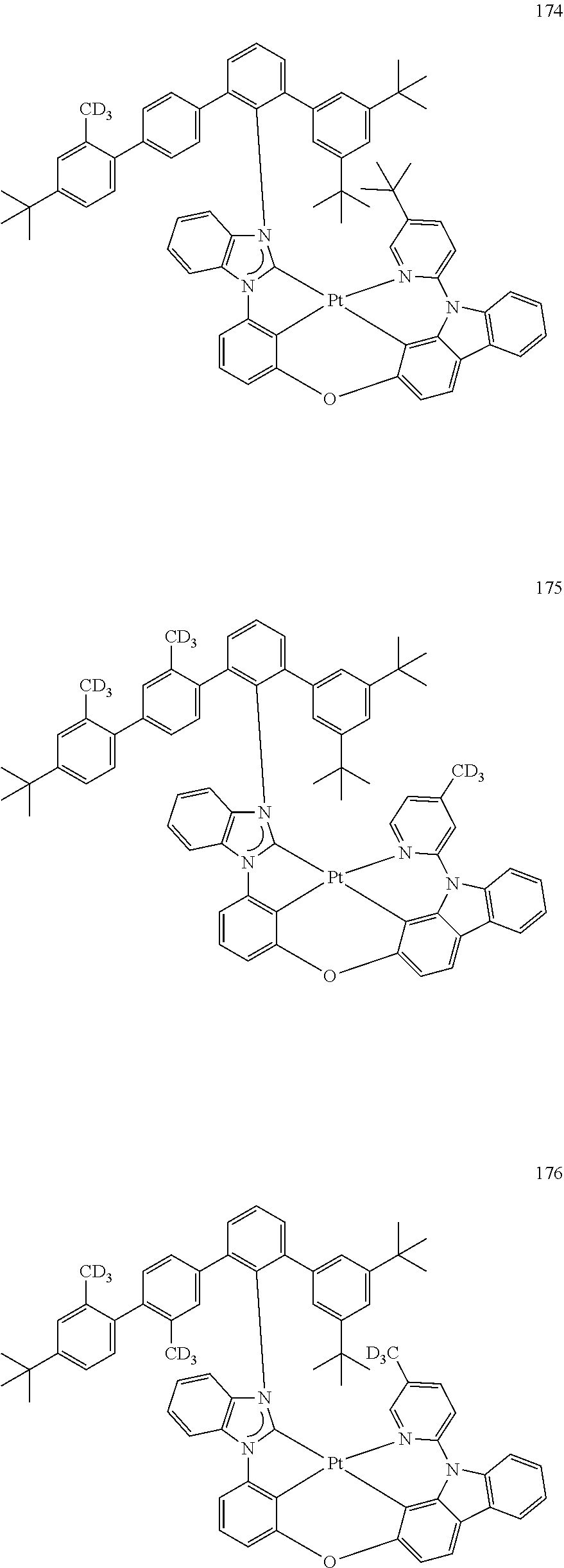


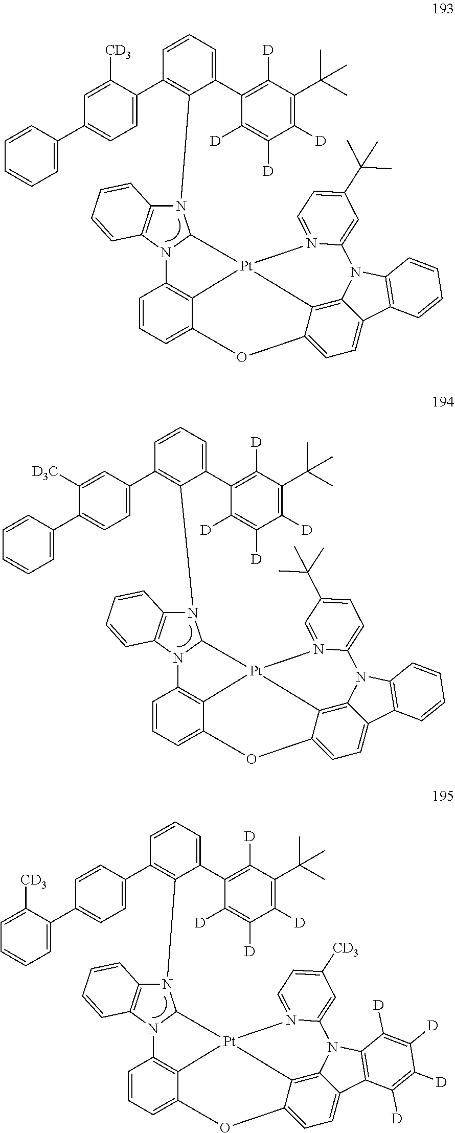
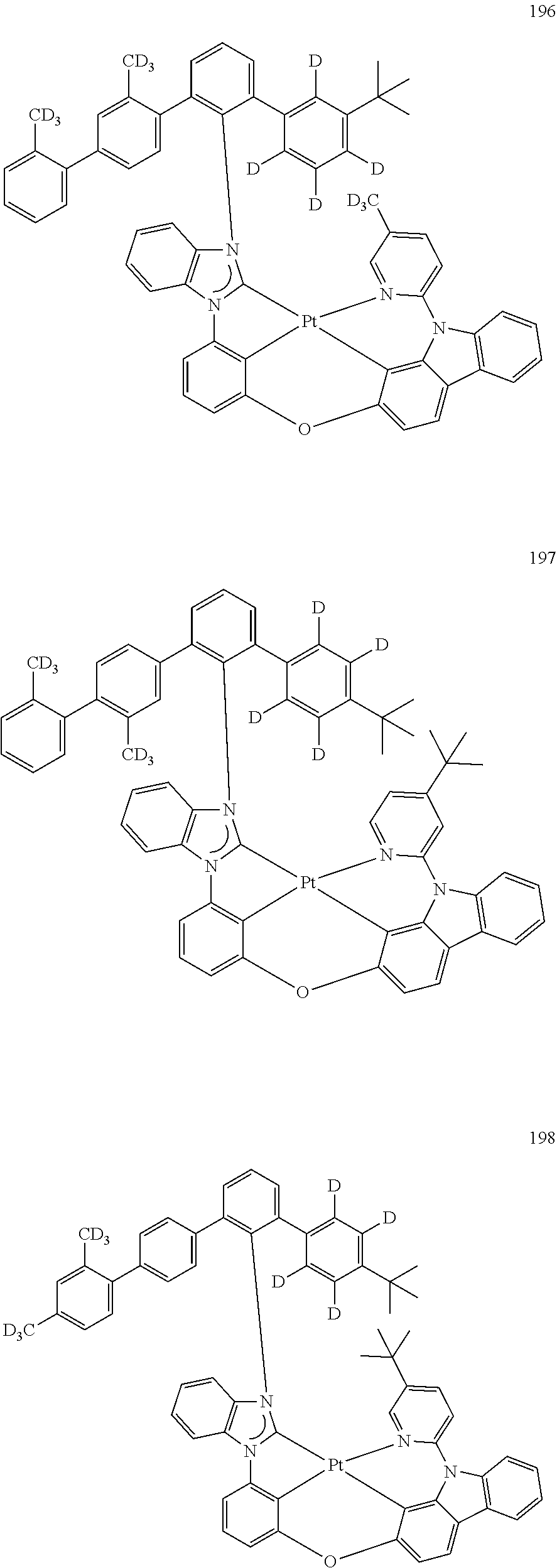
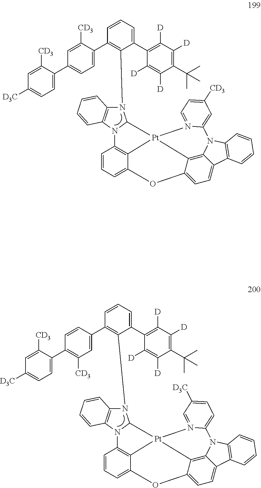
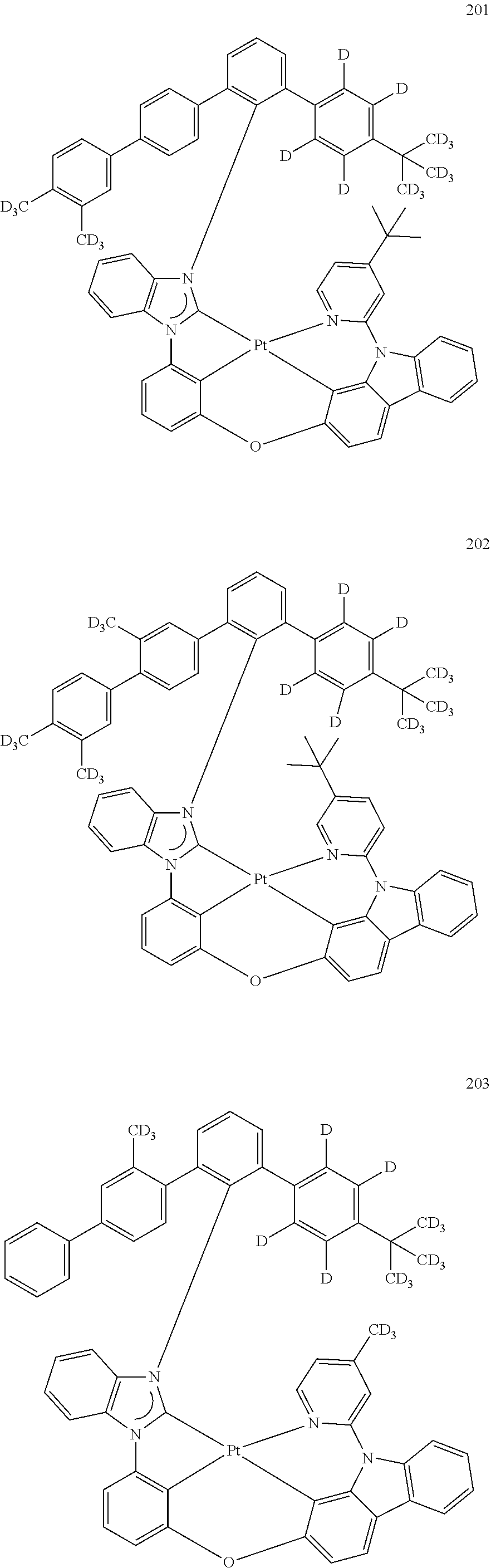


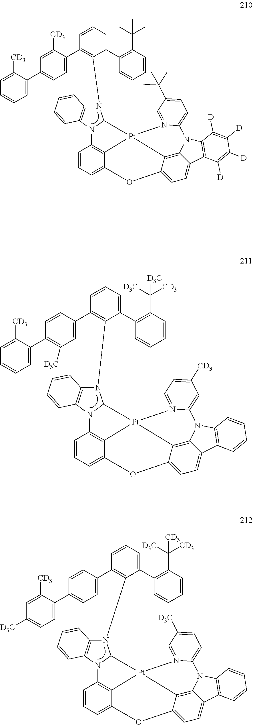


-
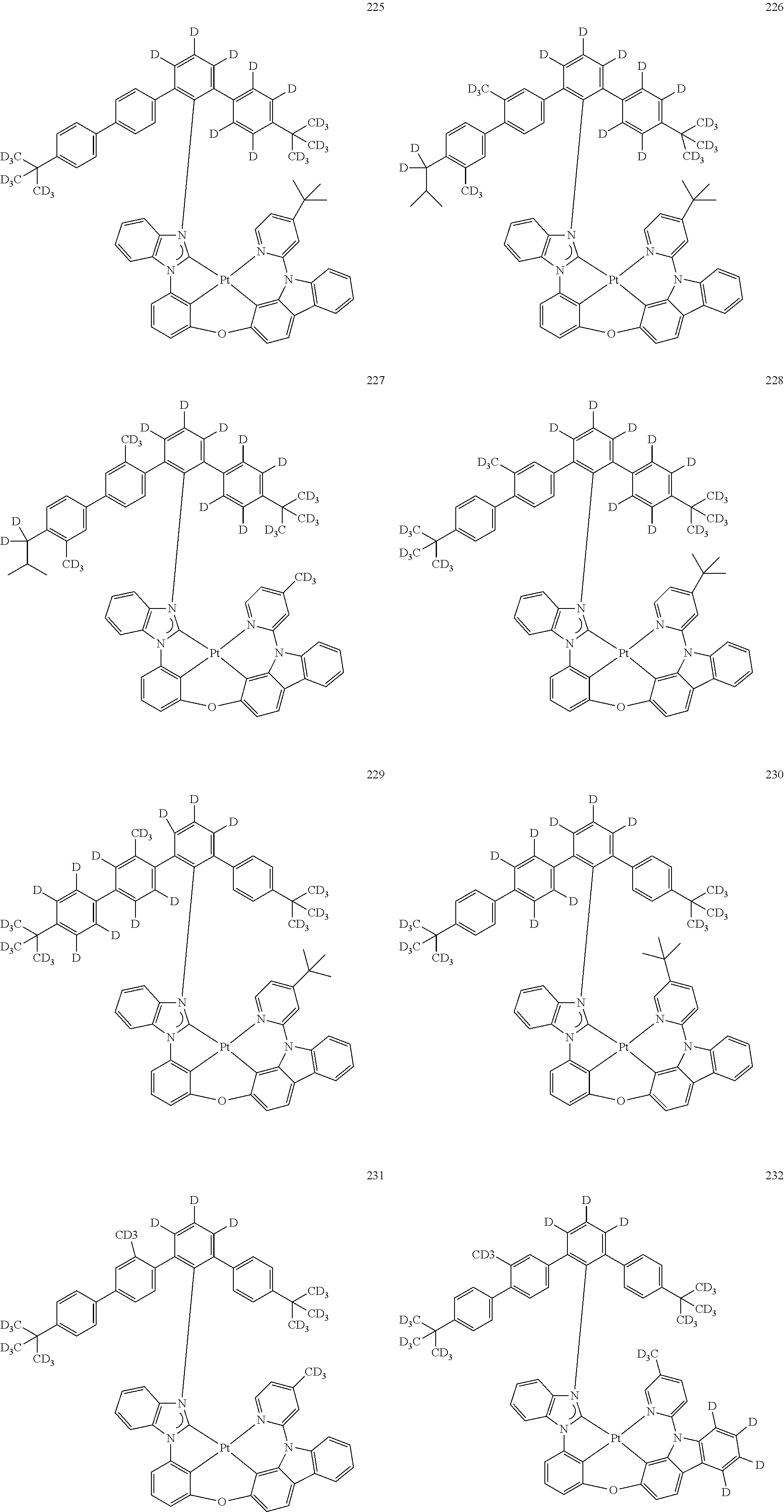


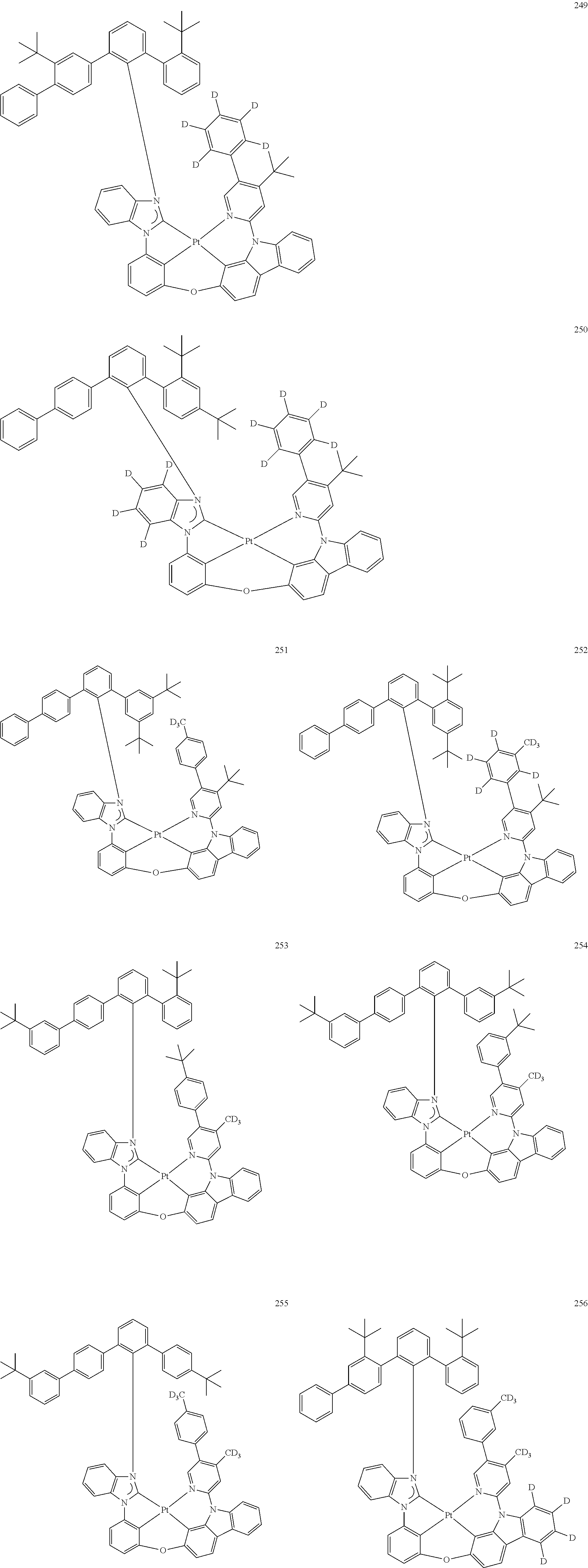
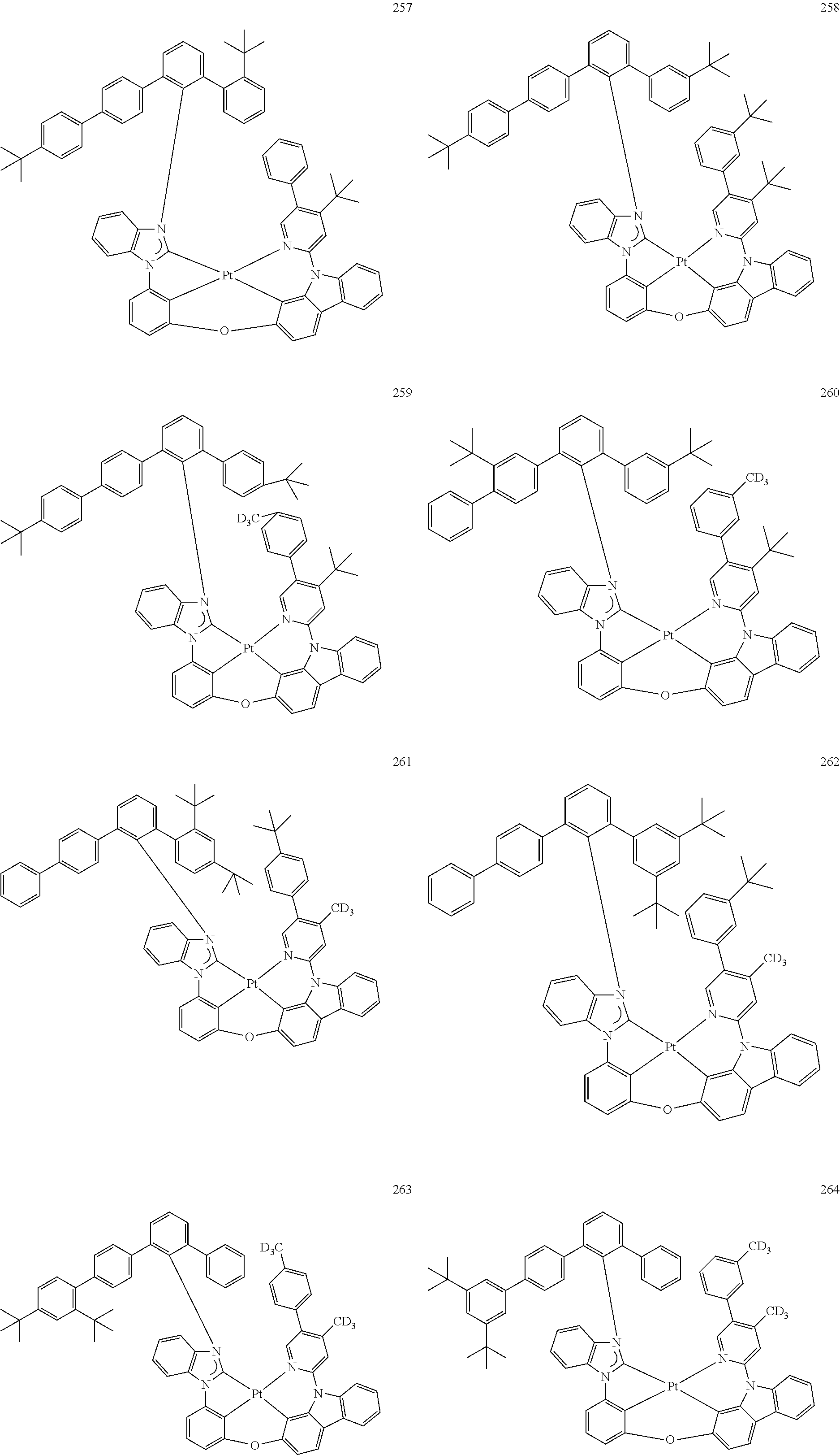
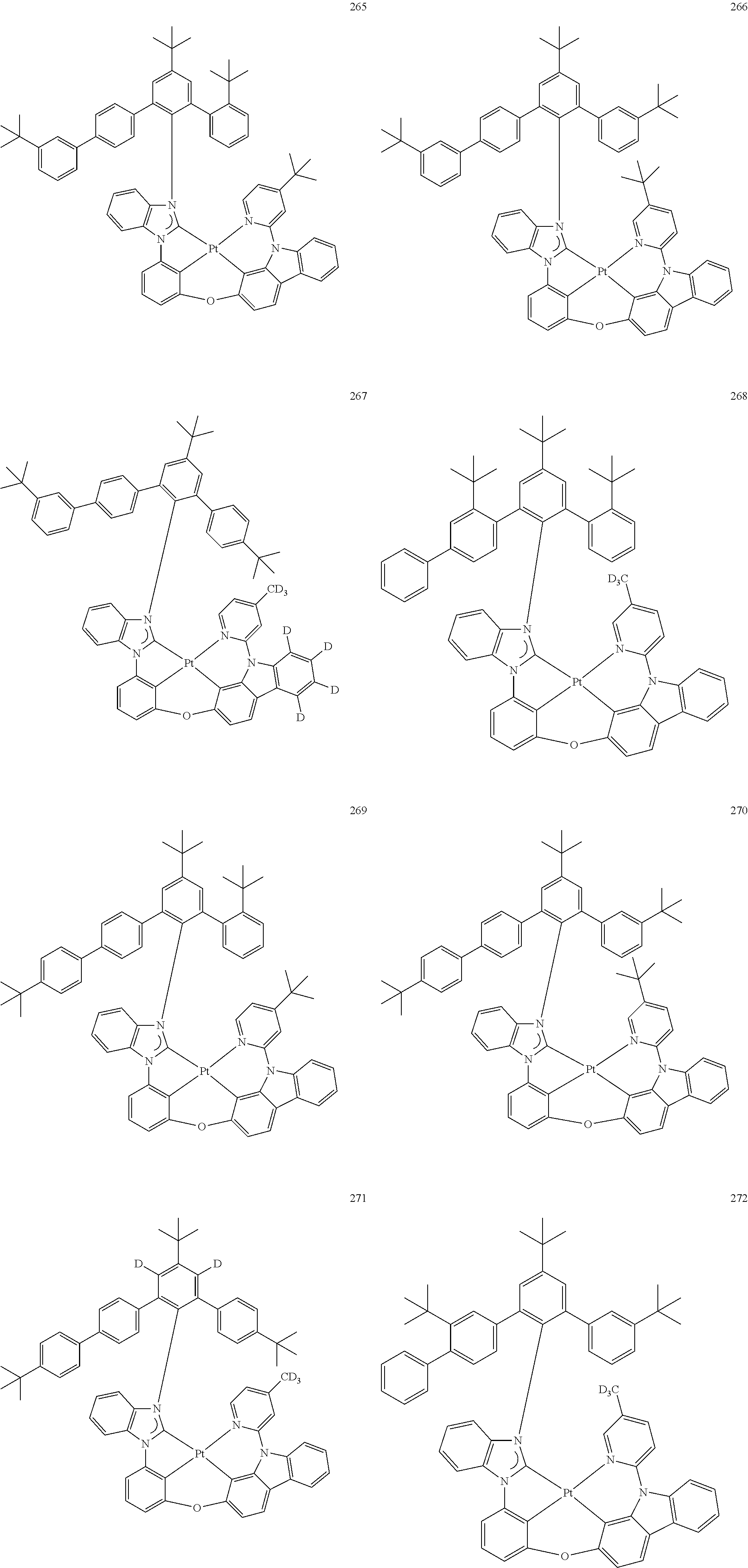
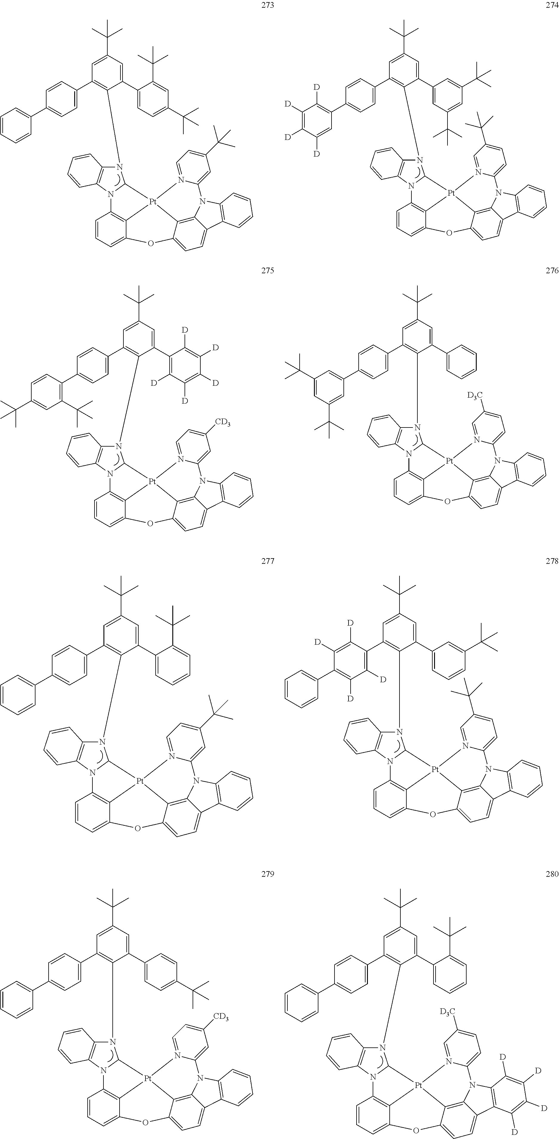
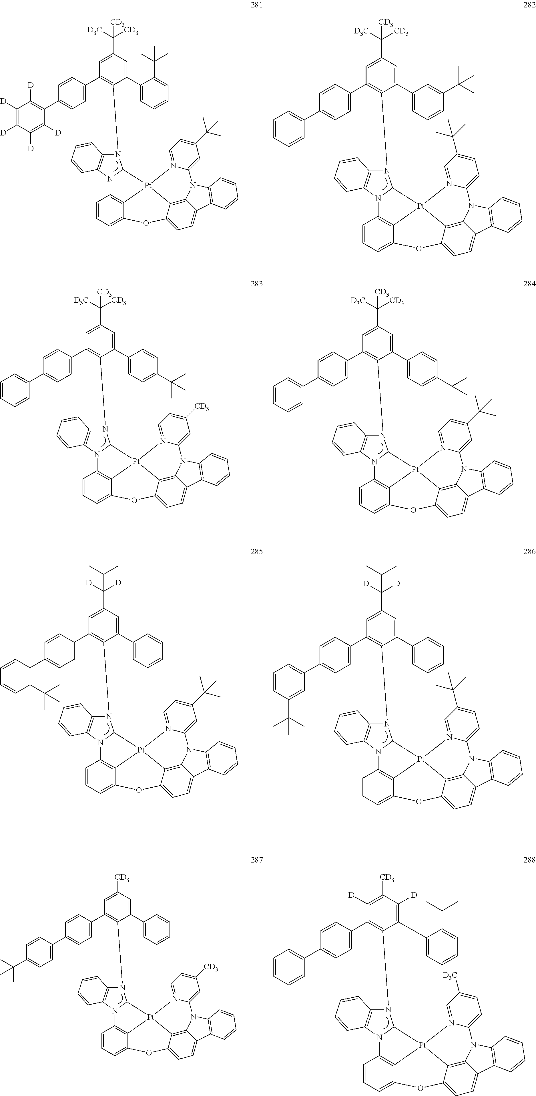
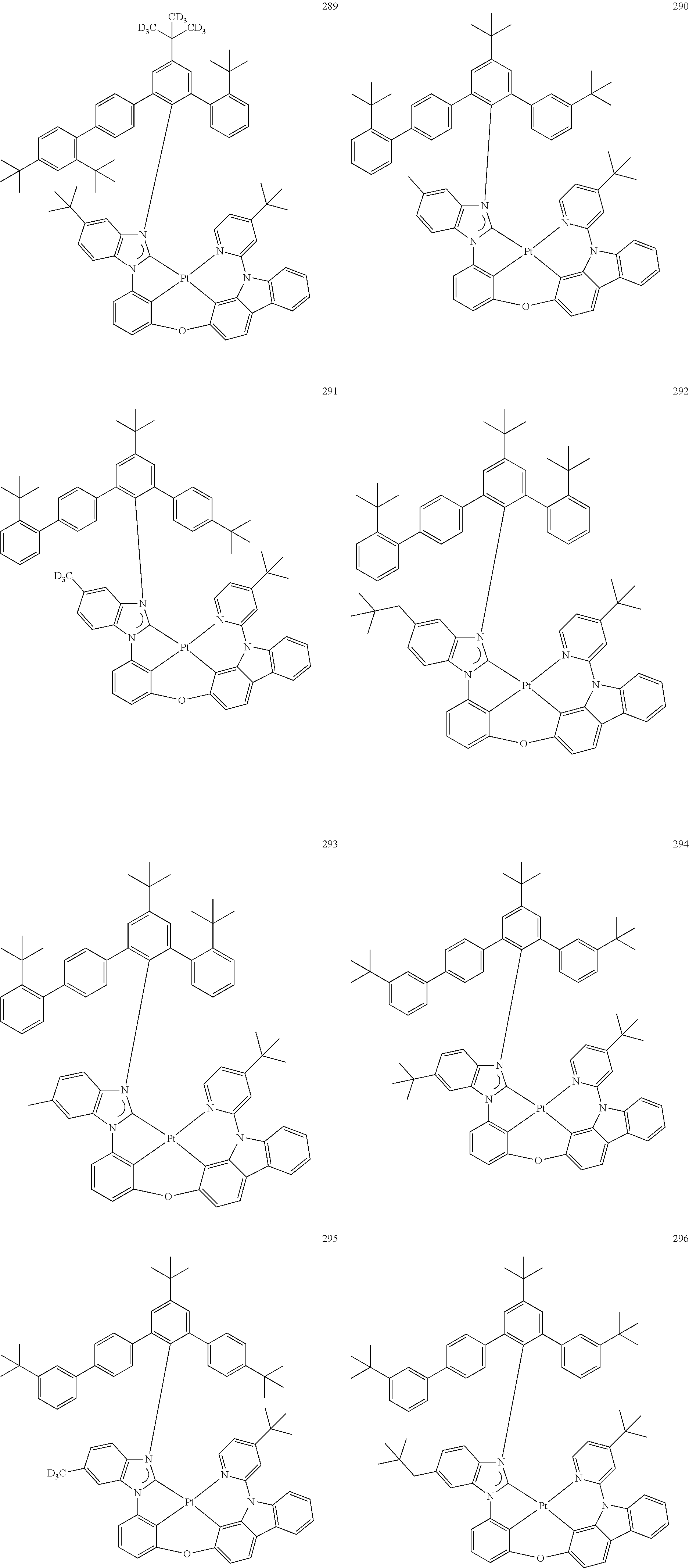


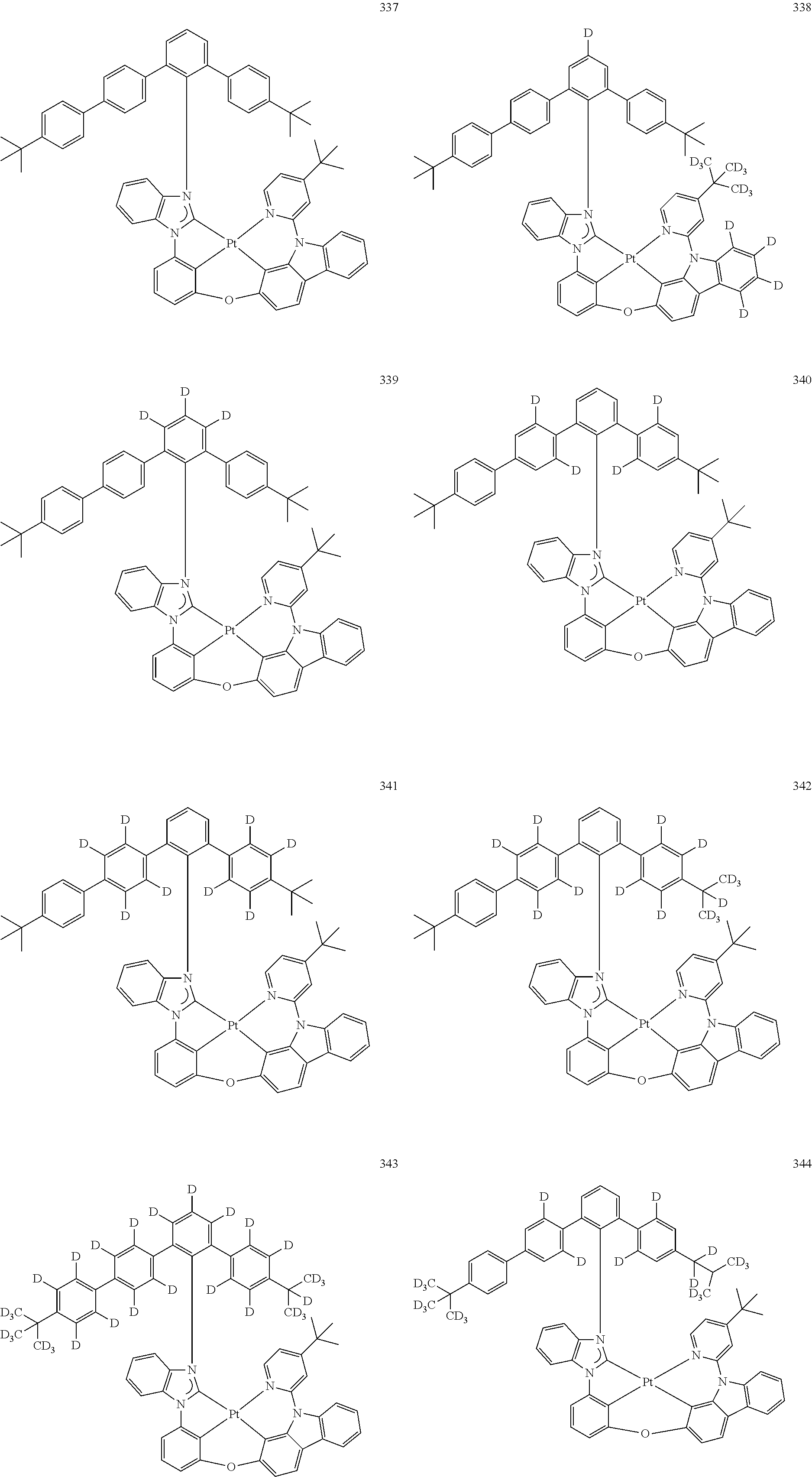
- In one or more embodiments, the second compound may be at least one of Compounds ETH1 to ETH100:
-
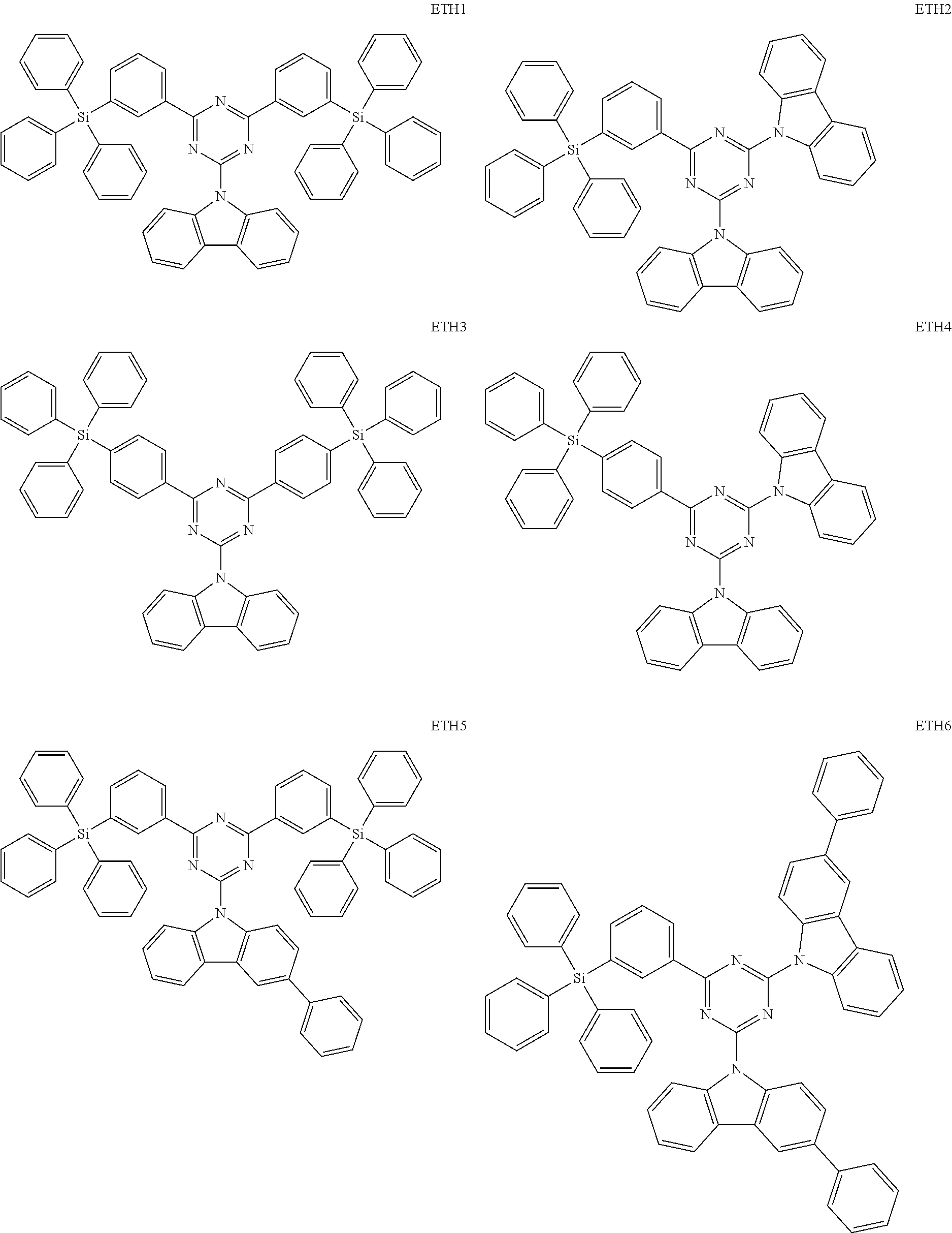

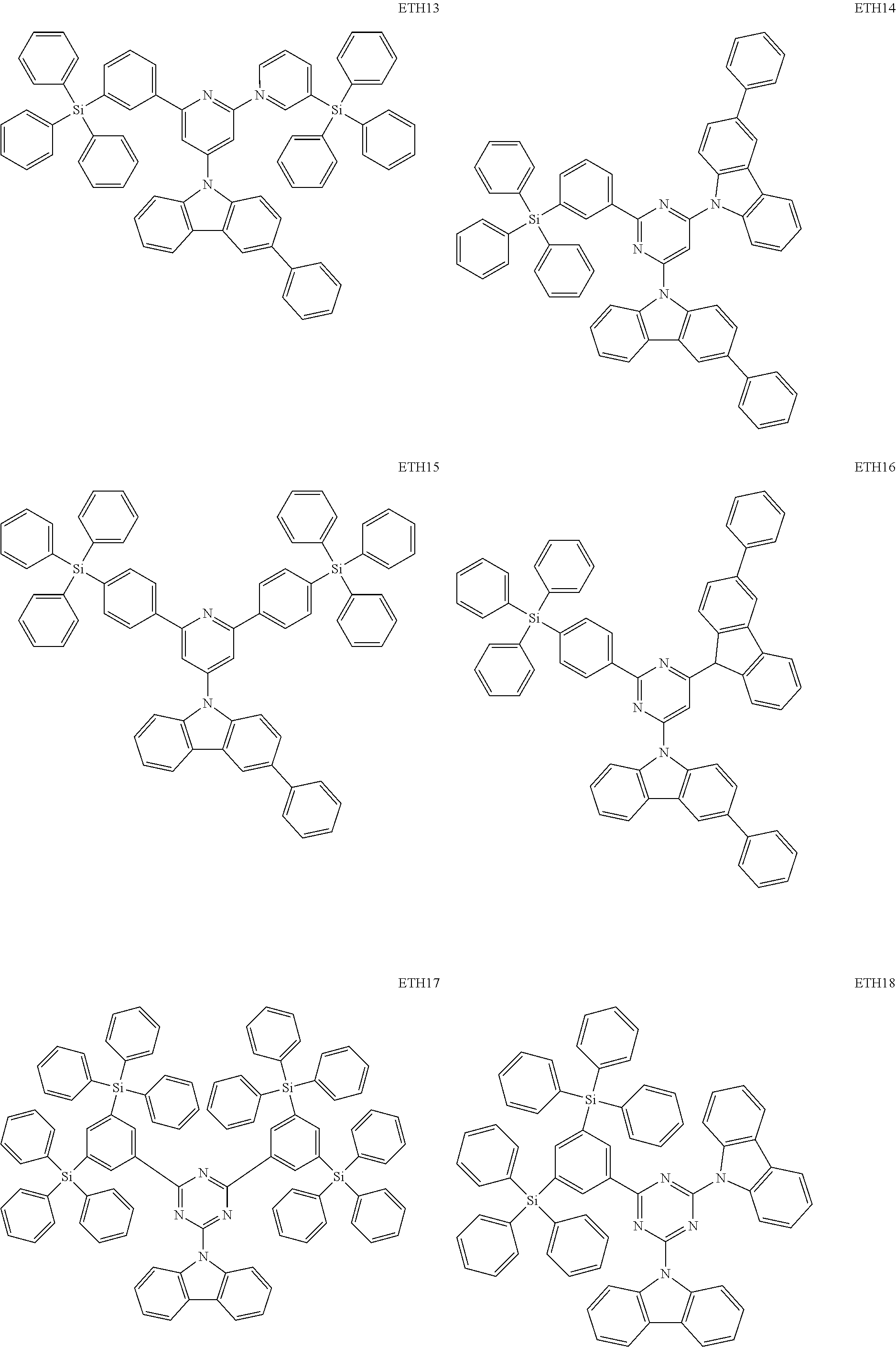
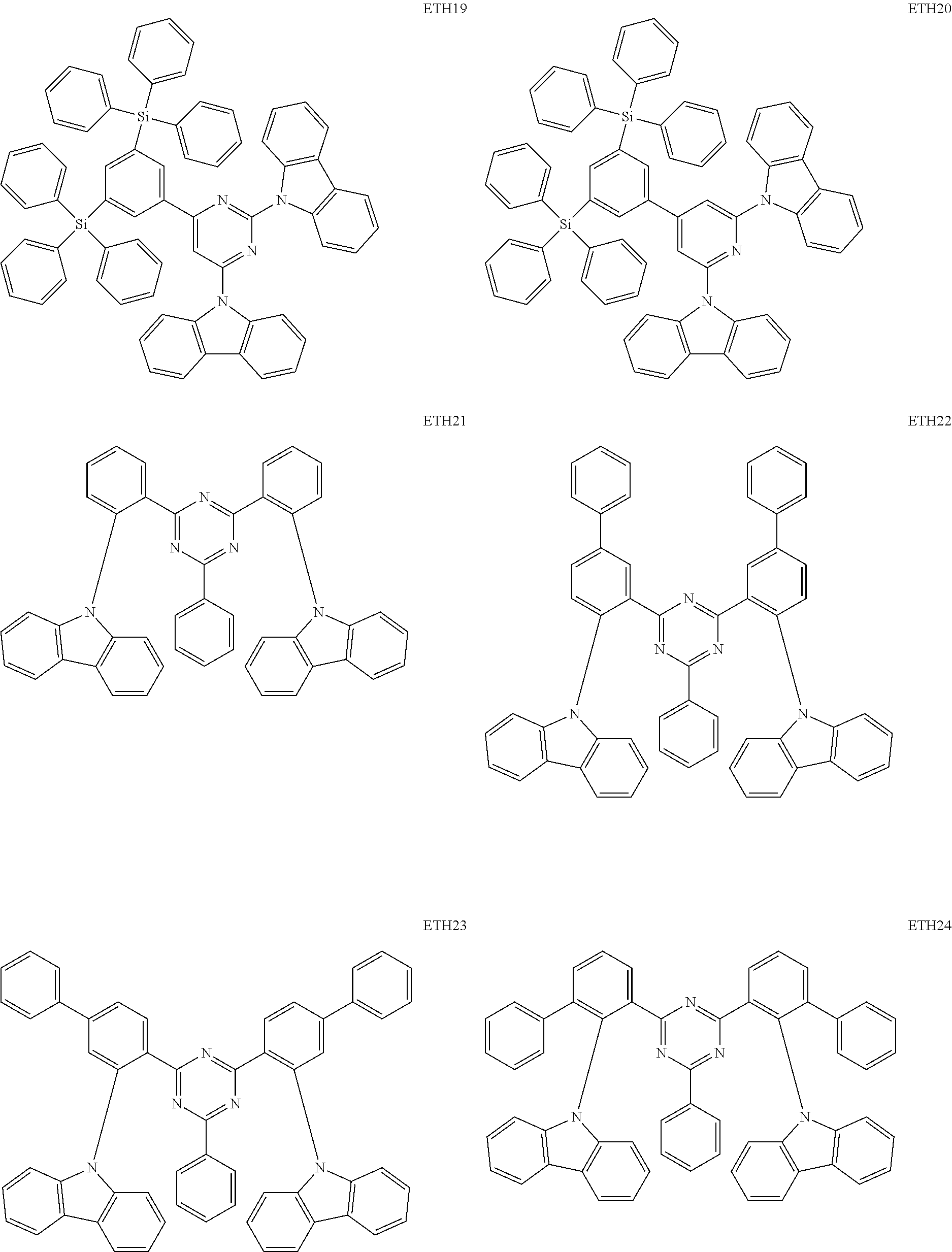
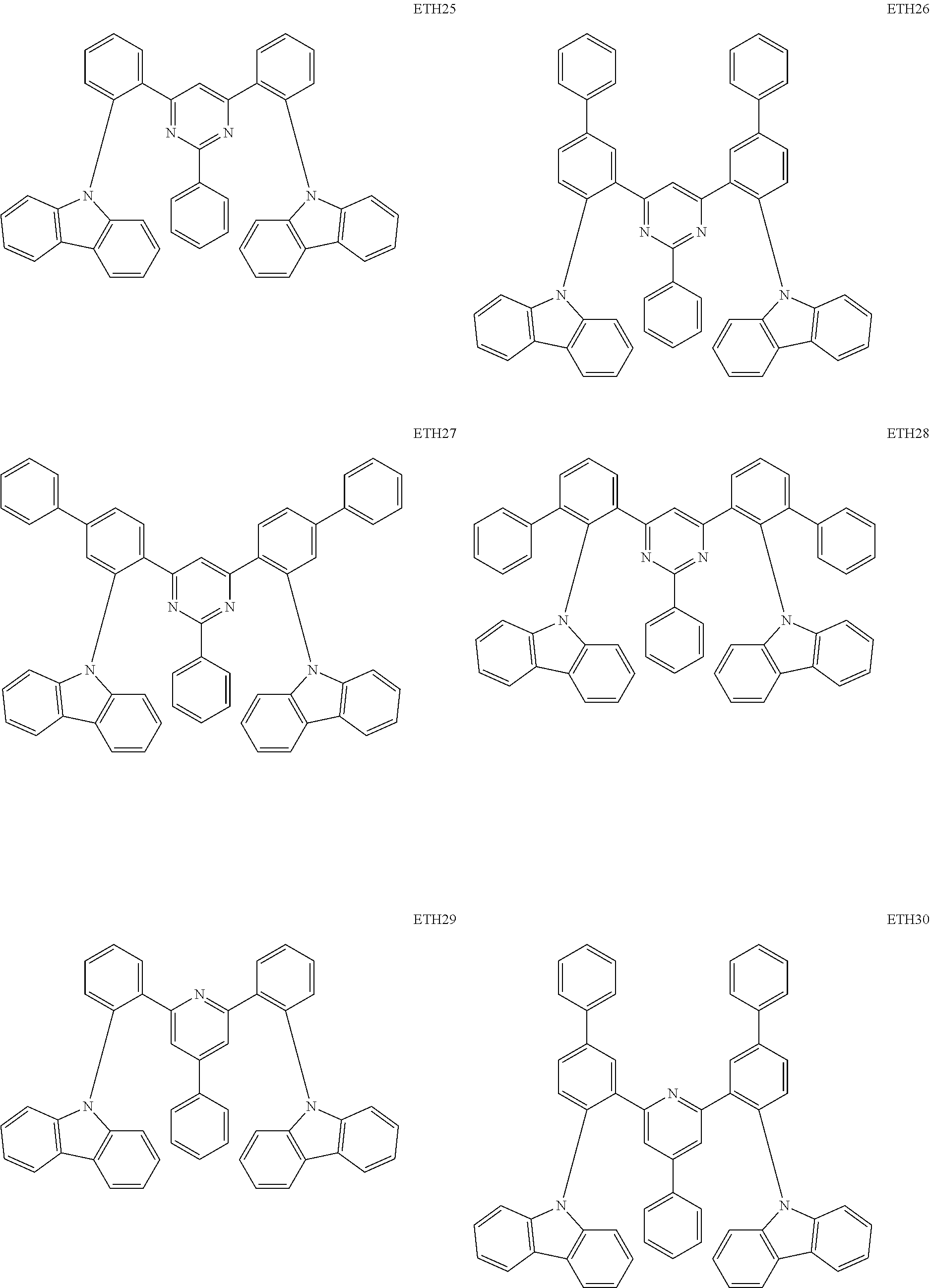


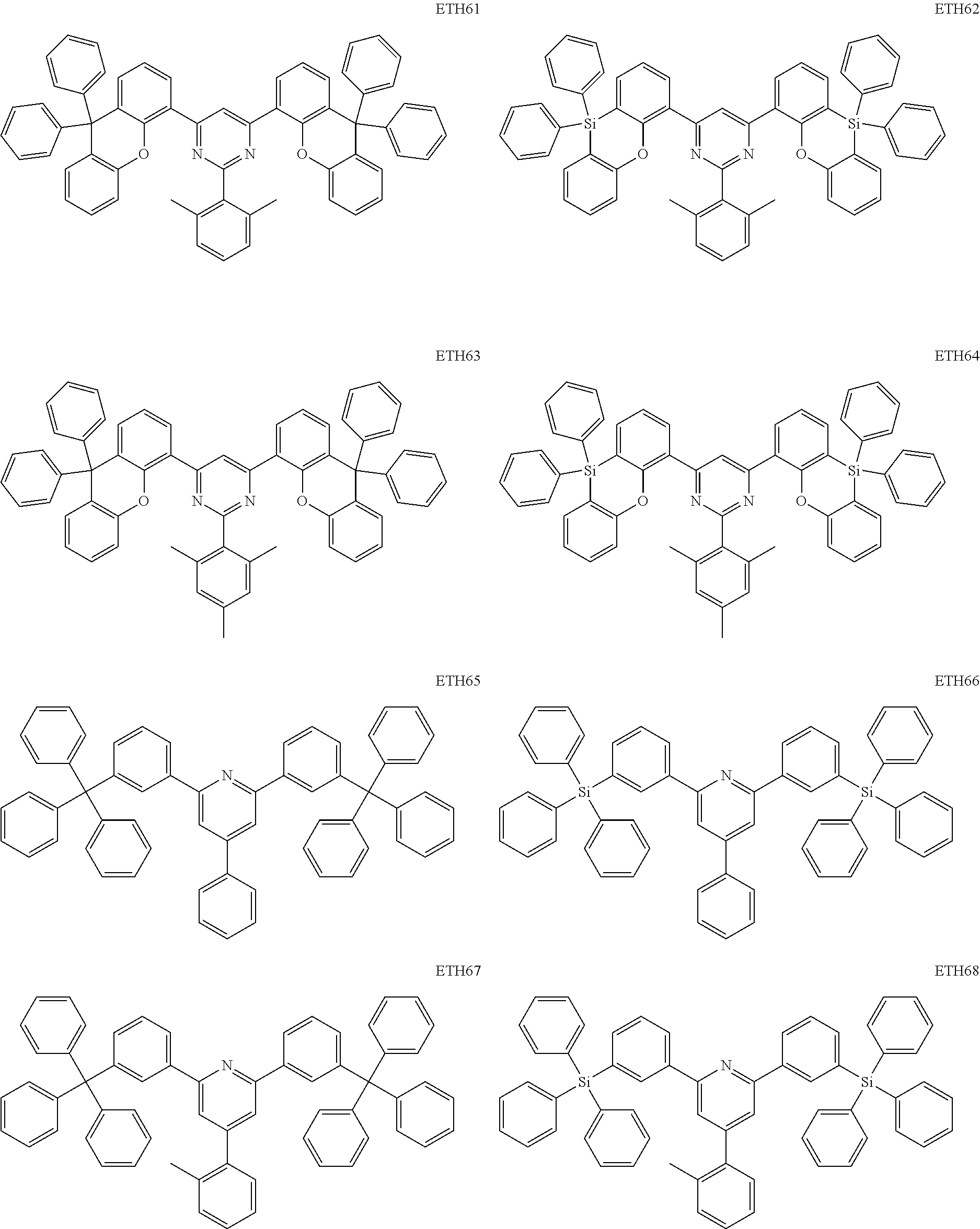
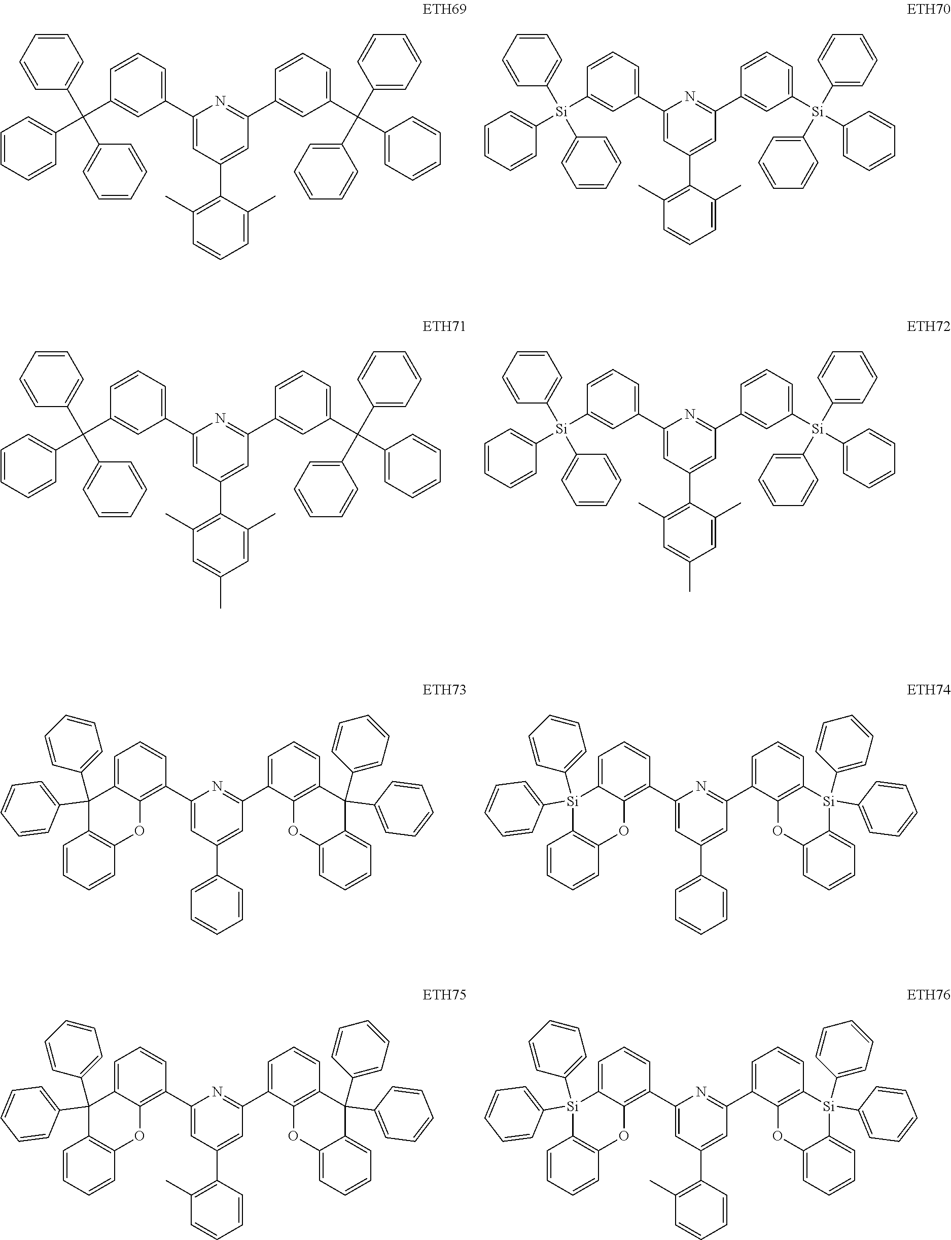
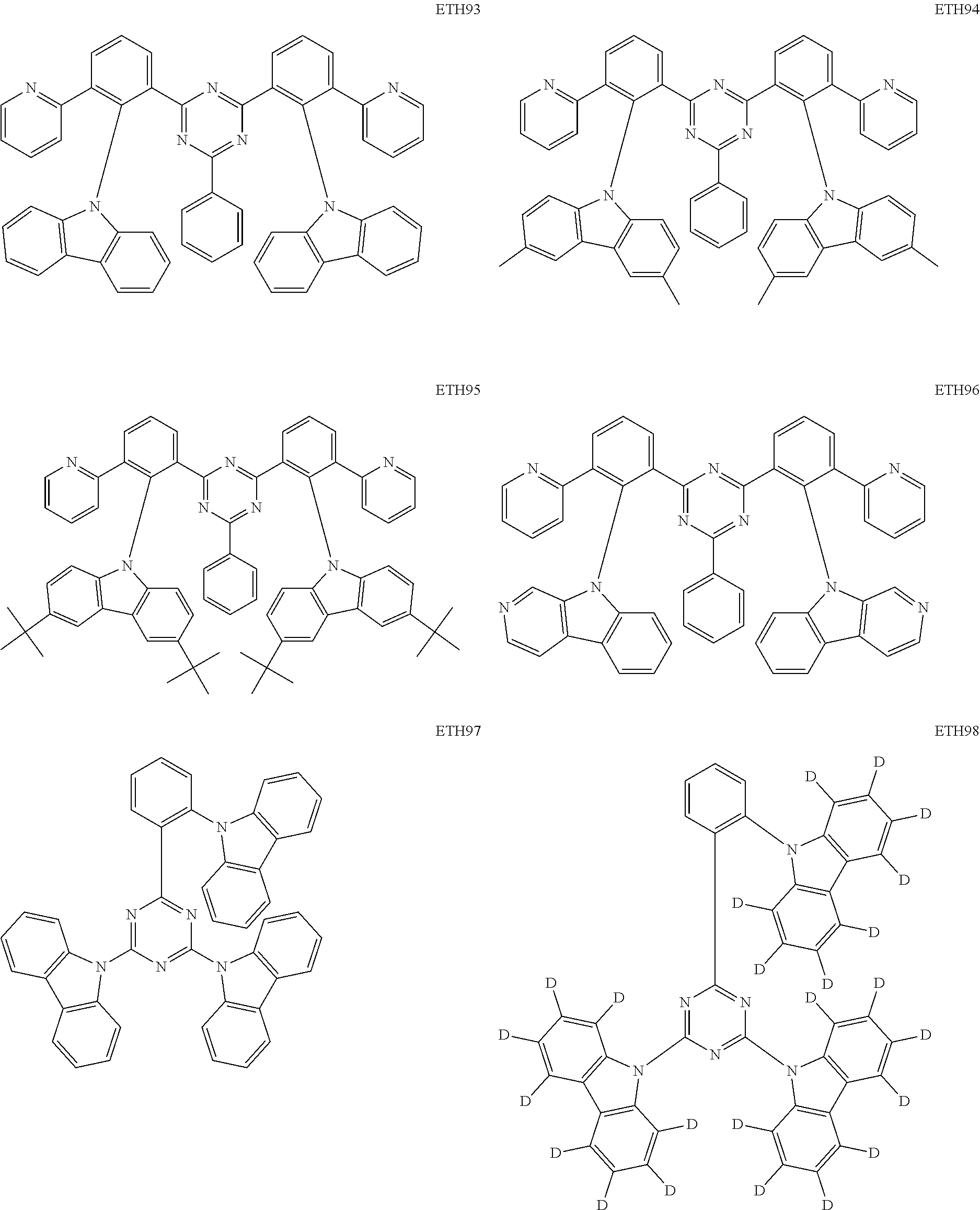

- In one or more embodiments, the third compound may be at least one of Compounds HTH1 to HTH46:
-


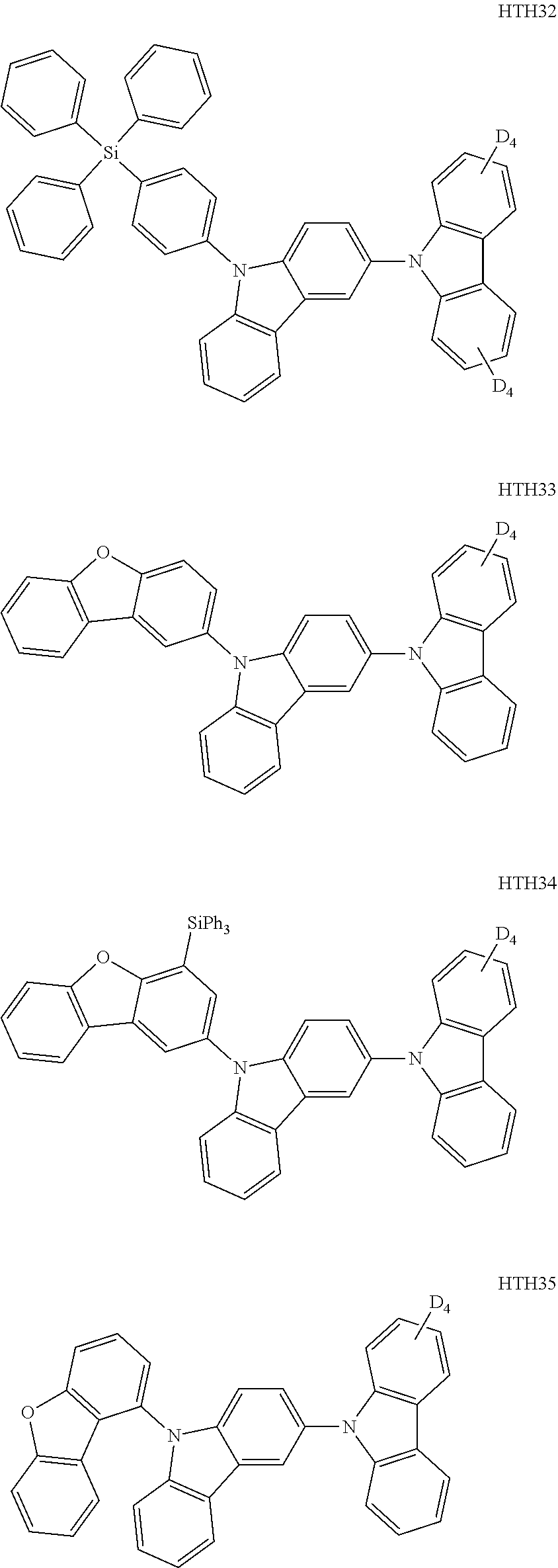


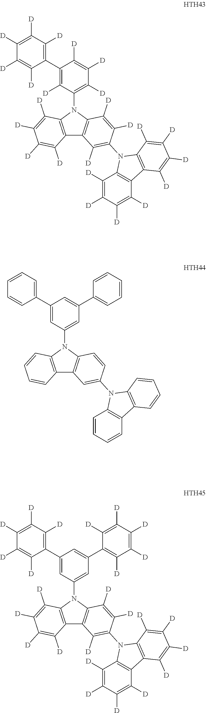

- In one or more embodiments, the fourth compound may be at least one of Compounds DFD1 to DFD29 and DFD051:
-

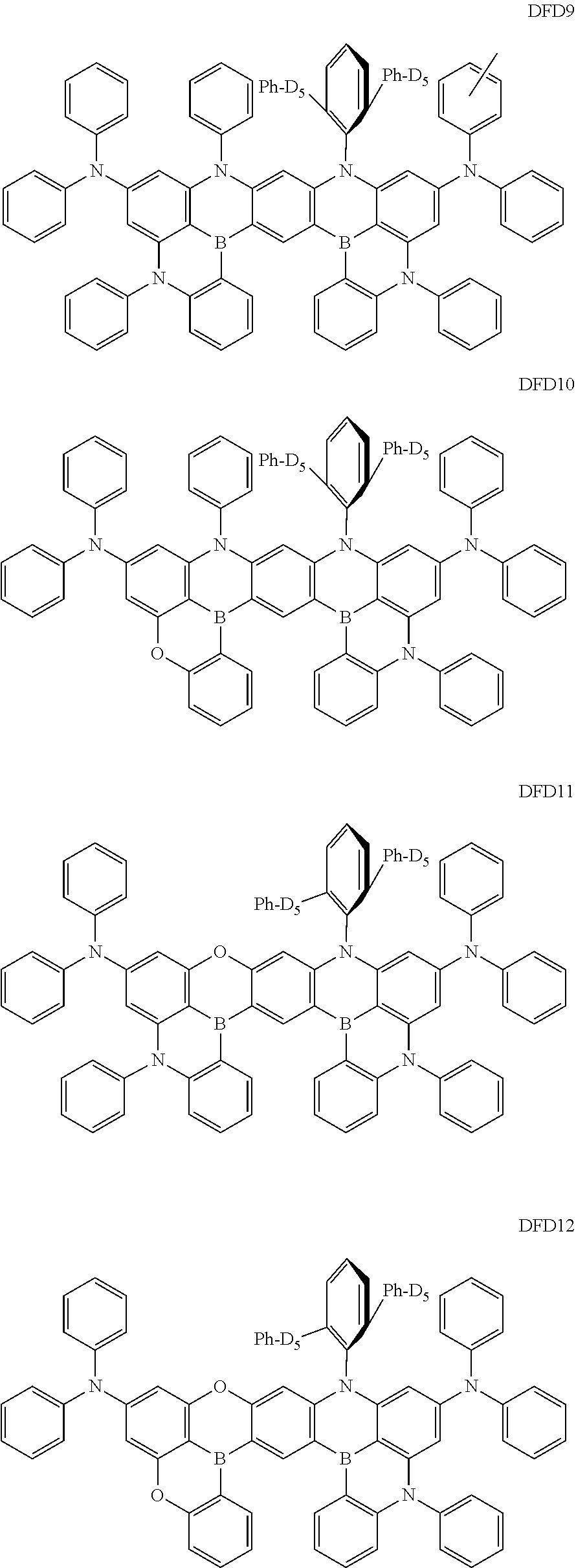
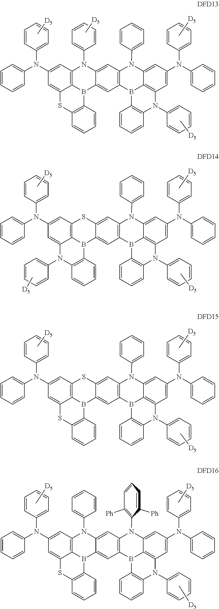


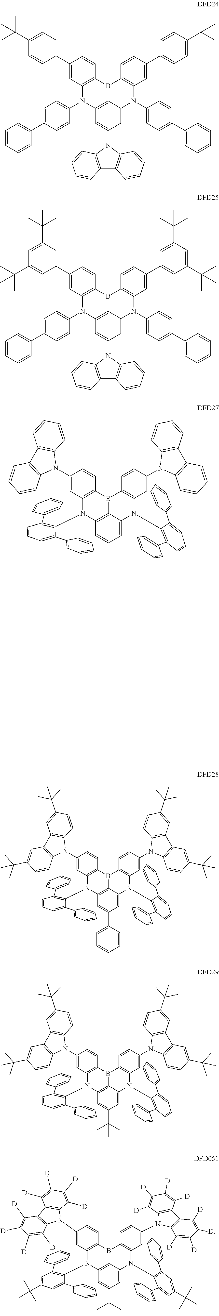
- In the preceding compounds described herein, Ph represents a phenyl group, D5 represents substitution with five deuteriums, and D4 represents substitution with four deuteriums. For example, a group represented by
-
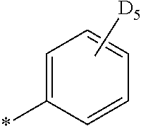
- may be identical to a group represented by
-
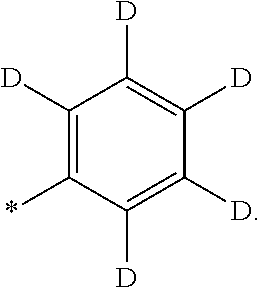
-
FIG. 1 is a schematic cross-sectional view of a light-emittingdevice 10 according to one or more embodiments. The light-emittingdevice 10 includes afirst electrode 110, aninterlayer 130, and asecond electrode 150. - Hereinafter, a structure of the light-emitting
device 10 according to one or more embodiments and a method of manufacturing the light-emittingdevice 10 will be described with reference toFIG. 1 . - In
FIG. 1 , a substrate may be additionally arranged under thefirst electrode 110 or on thesecond electrode 150. As the substrate, a glass substrate or a plastic substrate may be utilized. In one or more embodiments, the substrate may be a flexible substrate and may include plastics with excellent or suitable heat resistance and durability, such as polyimide, polyethylene terephthalate (PET), polycarbonate, polyethylene napthalate, polyarylate (PAR), polyetherimide, or any combination thereof. - The
first electrode 110 may be formed by, for example, depositing or sputtering a material for forming thefirst electrode 110 on the substrate. When thefirst electrode 110 is an anode, a material for forming thefirst electrode 110 may be a high-work function material that facilitates injection of holes. - The
first electrode 110 may be a reflective electrode, a semi-transmissive electrode, or a transmissive electrode. When thefirst electrode 110 is a transmissive electrode, a material for forming thefirst electrode 110 may include indium tin oxide (ITO), indium zinc oxide (IZO), tin oxide (SnO2), zinc oxide (ZnO), or any combination thereof. In one or more embodiments, when thefirst electrode 110 is a semi-transmissive electrode or a reflective electrode, a material for forming thefirst electrode 110 may include magnesium (Mg), silver (Ag), aluminum (Al), aluminum-lithium (Al—Li), calcium (Ca), magnesium-indium (Mg—In), magnesium-silver (Mg—Ag), or any combination thereof. - The
first electrode 110 may have a single-layer structure including (e.g., consisting of) a single layer or a multilayer structure including a plurality of layers. In one or more embodiments, thefirst electrode 110 may have a three-layer structure of ITO/Ag/ITO. - The
interlayer 130 may be arranged on thefirst electrode 110. Theinterlayer 130 may include the emission layer. - The
interlayer 130 may further include a hole transport region arranged between thefirst electrode 110 and the emission layer, and an electron transport region arranged between the emission layer and thesecond electrode 150. - The
interlayer 130 may further include, in addition to one or more suitable organic materials, a metal-containing compound such as an organometallic compound, an inorganic material such as quantum dots, and/or the like. - In one or more embodiments, the
interlayer 130 may include i) two or more emitting units sequentially stacked between thefirst electrode 110 and thesecond electrode 150, and ii) a charge generation layer located between two neighboring emitting units. When theinterlayer 130 includes emitting units and a charge generation layer as described herein, the light-emittingdevice 10 may be a tandem light-emitting device. - The hole transport region may have: i) a single-layer structure including (e.g., consisting of) a single layer including (e.g., consisting of) a single material, ii) a single-layer structure including (e.g., consisting of) a single layer including (e.g., consisting of) a plurality of materials that are different from each other, or iii) a multilayer structure including a plurality of layers including a plurality of materials that are different from each other.
- The hole transport region may include a hole injection layer, a hole transport layer, an emission auxiliary layer, an electron blocking layer, or any combination thereof.
- In one or more embodiments, the hole transport region may have a multilayer structure including a hole injection layer/hole transport layer structure, a hole injection layer/hole transport layer/emission auxiliary layer structure, a hole injection layer/emission auxiliary layer structure, a hole transport layer/emission auxiliary layer structure, or a hole injection layer/hole transport layer/electron blocking layer structure, wherein constituent layers of each structure are stacked sequentially from the
first electrode 110. - The hole transport region may include a compound represented by Formula 201, a compound represented by Formula 202, and/or any combination thereof:
-

-
- wherein, in Formulae 201 and 202,
- L201 to L204 may each independently be a C3-C60 carbocyclic group that is unsubstituted or substituted with at least one R10a or a C1-C60 heterocyclic group that is unsubstituted or substituted with at least one R10a,
- L205 may be *—O—*′, *—S—*′, *—N(Q201)-*′, a C1-C20 alkylene group that is unsubstituted or substituted with at least one R10a, a C2-C20 alkenylene group that is unsubstituted or substituted with at least one R10a, a C3-C60 carbocyclic group that is unsubstituted or substituted with at least one R10a, or a C1-C60 heterocyclic group that is unsubstituted or substituted with at least one R10a,
- xa1 to xa4 may each independently be an integer from 0 to 5,
- xa5 may be an integer from 1 to 10,
- R201 to R204 and Q201 may each independently be a C3-C60 carbocyclic group that is unsubstituted or substituted with at least one R10a or a C1-C60 heterocyclic group that is unsubstituted or substituted with at least one R10a,
- R201 and R202 may optionally be linked to each other via a single bond, a C1-C5 alkylene group that is unsubstituted or substituted with at least one R10a, or a C2-C5 alkenylene group that is unsubstituted or substituted with at least one R10a to form a C8-C60 polycyclic group (e.g., a carbazole group and/or the like) unsubstituted or substituted with at least one R10a (e.g., see Compound HT16),
- R203 and R204 may optionally be linked to each other via a single bond, a C1-C5 alkylene group that is unsubstituted or substituted with at least one R10a, or a C2-C5 alkenylene group that is unsubstituted or substituted with at least one R10a to form a C8-C60 polycyclic group that is unsubstituted or substituted with at least one R10a, and
- na1 may be an integer from 1 to 4.
- In one or more embodiments, each of Formulae 201 and 202 may include at least one of groups represented by Formulae CY201 to CY217:
-
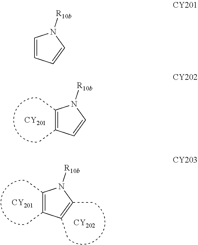
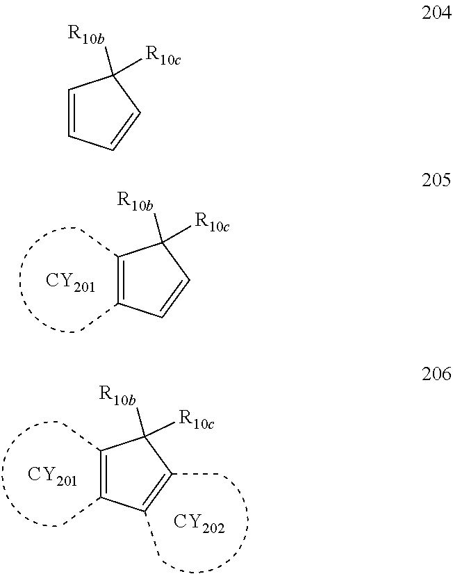
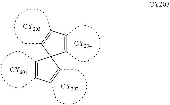
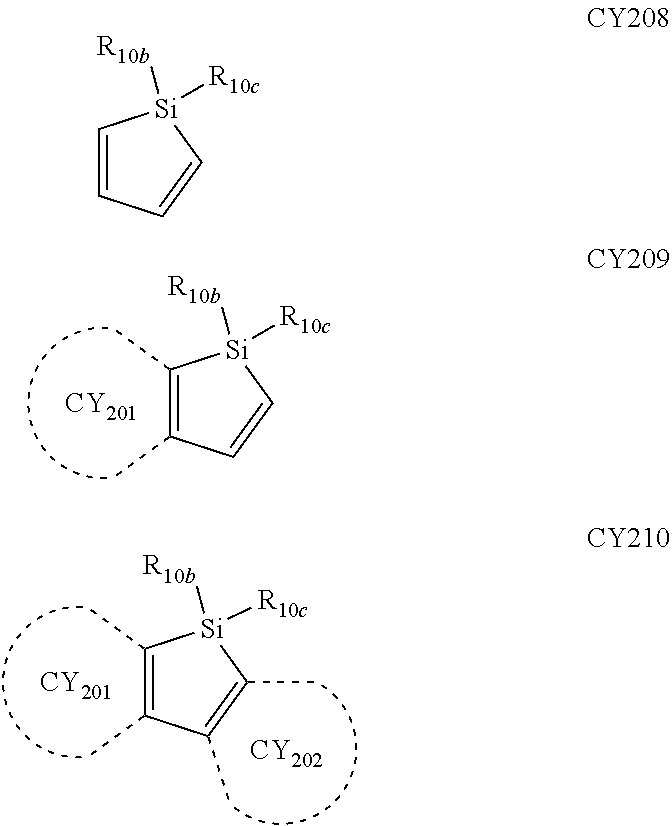

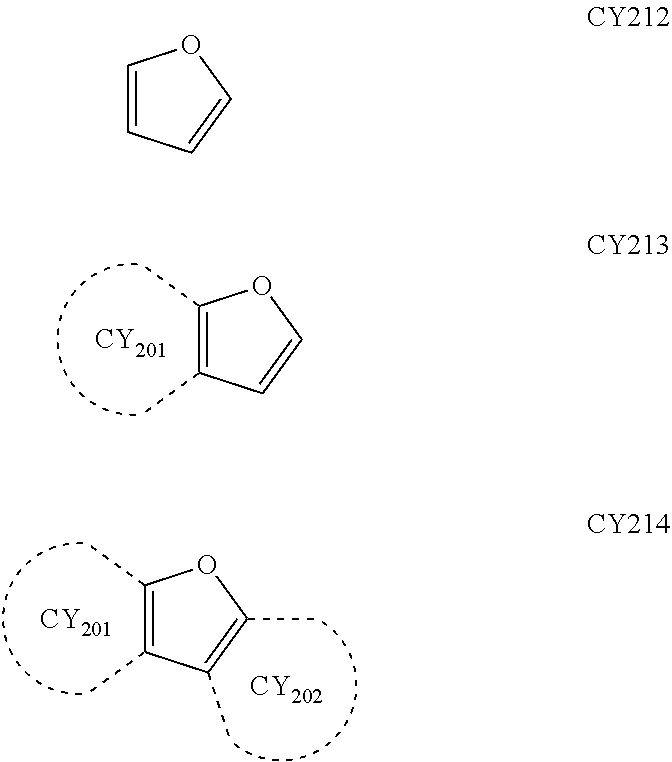

- In Formulae CY201 to CY217, R10b, and R10c are each as described in connection with R10a, ring CY201 to ring CY204 may each independently be a C3-C20 carbocyclic group or a C1-C20 heterocyclic group, and at least one hydrogen in Formulae CY201 to CY217 may be unsubstituted or substituted with R10a.
- In one or more embodiments, ring CY201 to ring CY204 in Formulae CY201 to CY217 may each independently be a benzene group, a naphthalene group, a phenanthrene group, or an anthracene group.
- In one or more embodiments, each of Formulae 201 and 202 may include at least one of groups represented by Formulae CY201 to CY203.
- In one or more embodiments, Formula 201 may include at least one of groups represented by Formulae CY201 to CY203 and at least one of groups represented by Formulae CY204 to CY217.
- In one or more embodiments, in Formula 201, xa1 may be 1, R201 may be a group represented by one of Formulae CY201 to CY203, xa2 may be 0, and R202 may be a group represented by one of Formulae CY204 to CY207.
- In one or more embodiments, each of Formulae 201 and 202 may not include (e.g., may exclude) groups represented by Formulae CY201 to CY203.
- In one or more embodiments, each of Formulae 201 and 202 may not include (e.g., may exclude) groups represented by Formulae CY201 to CY203 and may include at least one of groups represented by Formulae CY204 to CY217.
- In one or more embodiments, each of Formulae 201 and 202 may not include (e.g., may exclude) groups represented by Formulae CY201 to CY217.
- In one or more embodiments, the hole transport region may include at least one selected from among Compounds HT1 to HT46, m-MTDATA, TDATA, 2-TNATA, NPB(NPD), β-NPB, TPD, Spiro-TPD, Spiro-NPB, methylated NPB, TAPC, HMTPD, 4,4′,4″-tris(N-carbazolyl)triphenylamine (TCTA), polyaniline/dodecylbenzene sulfonic acid (PANI/DBSA), poly(3,4-ethylene dioxythiophene)/poly(4-styrene sulfonate) (PEDOT/PSS), polyaniline/camphor sulfonic acid (PANI/CSA), polyaniline/poly(4-styrene sulfonate) (PANI/PSS), and/or any combination thereof:
-

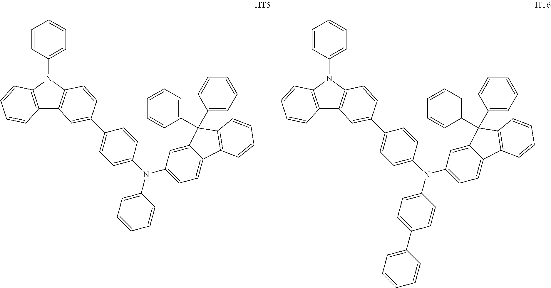
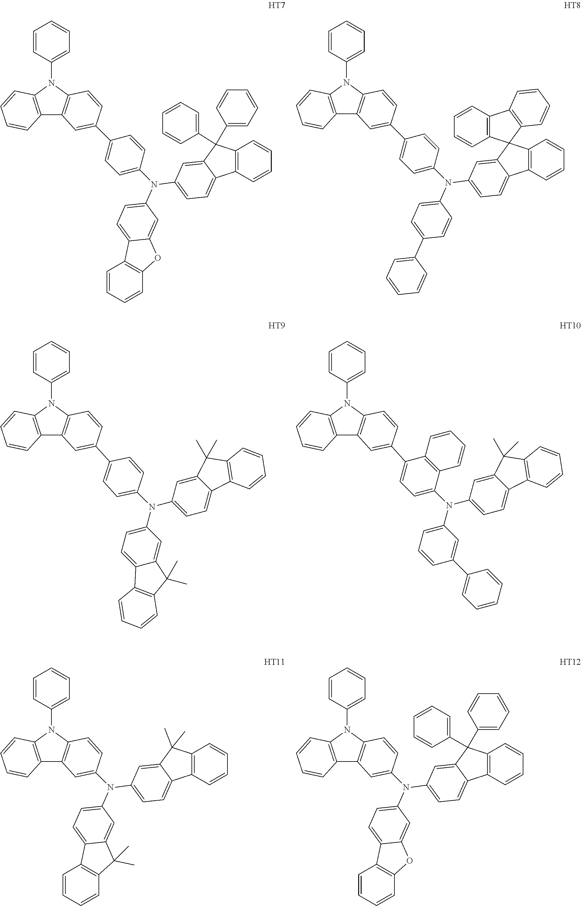
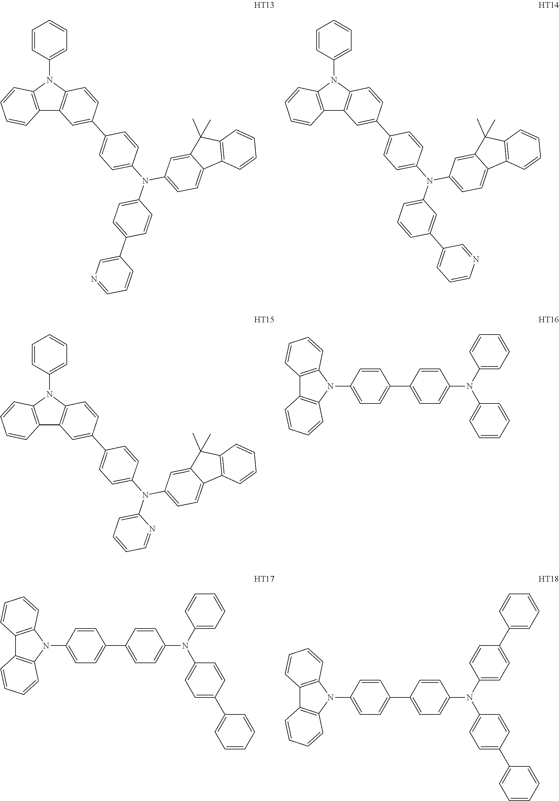
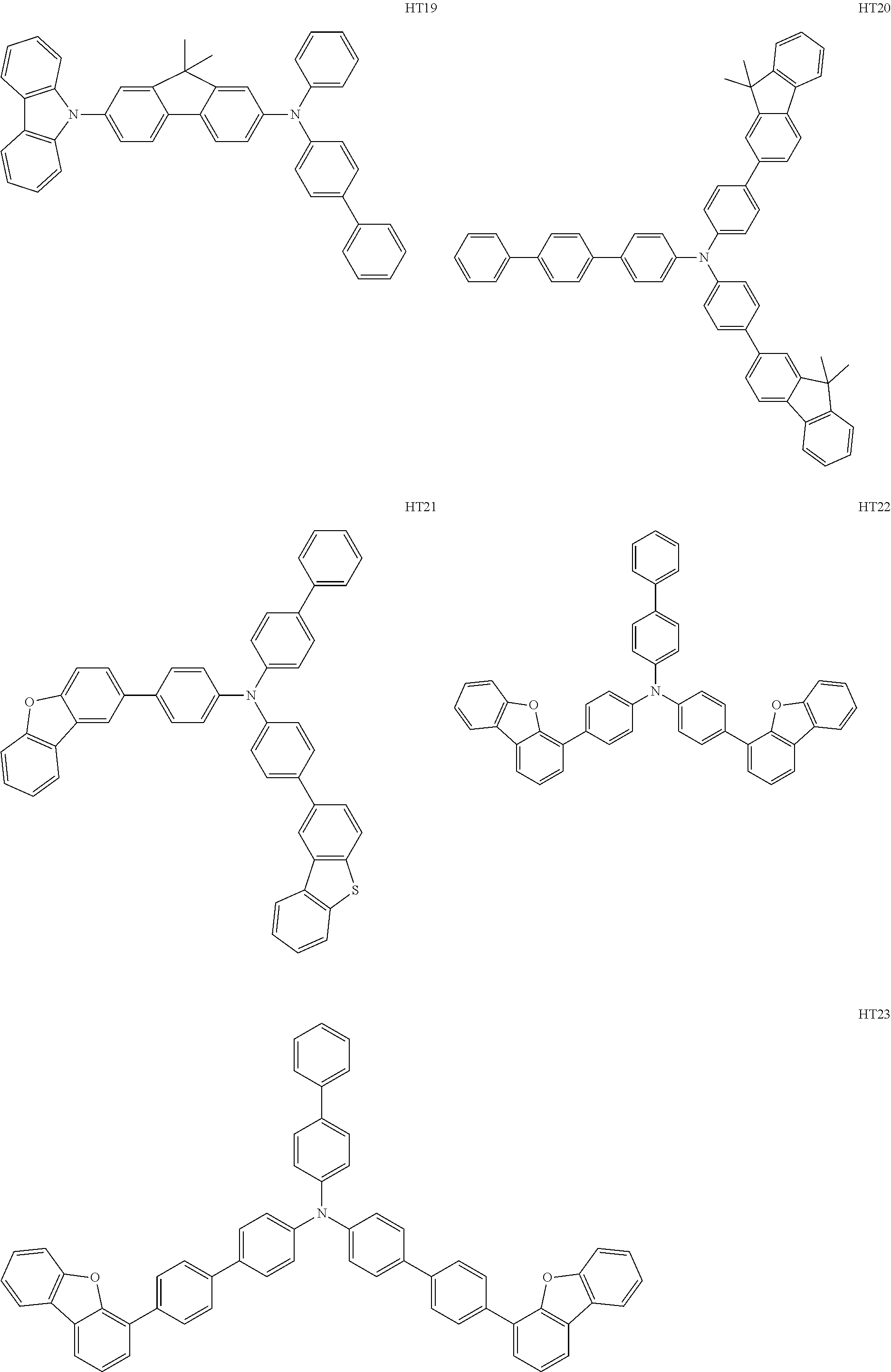


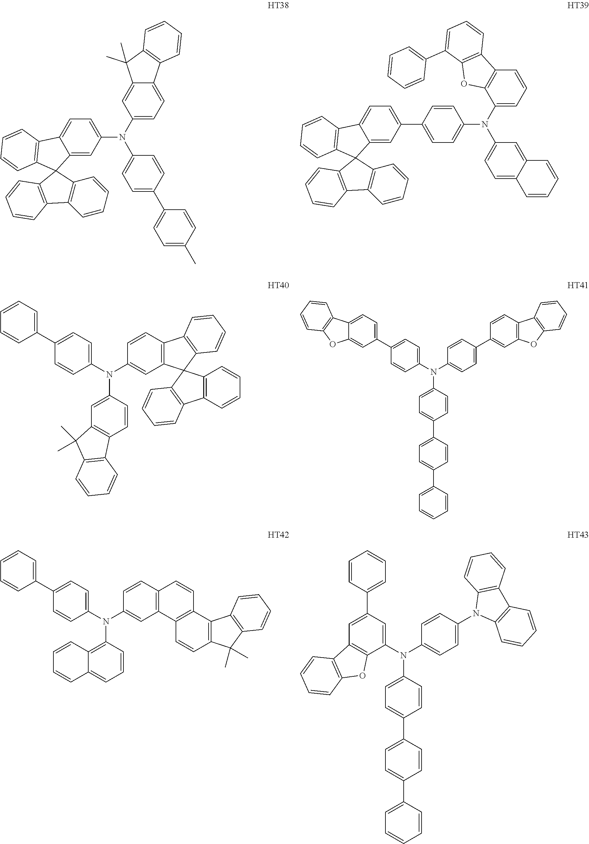


- The thickness of the hole transport region may be about 50 Å to about 10,000 Å, for example, about 100 Å to about 4,000 Å. When the hole transport region includes a hole injection layer, a hole transport layer, or any combination thereof, a thickness of the hole injection layer may be about 100 Å to about 9,000 Å, for example, about 100 Å to about 1,000 Å, and a thickness of the hole transport layer may be about 50 Å to about 2,000 Å, for example, about 100 Å to about 1,500 Å. When the thicknesses of the hole transport region, the hole injection layer, and the hole transport layer are within the ranges described herein, satisfactory hole transporting characteristics may be obtained without a substantial increase in driving voltage.
- The emission auxiliary layer may increase light-emission efficiency by compensating for an optical resonance distance according to the wavelength of light emitted by the emission layer, and the electron blocking layer may block or reduce the leakage of electrons from the emission layer to the hole transport region. Materials that may be included in the hole transport region may be included in the emission auxiliary layer and the electron blocking layer.
- p-Dopant
- The hole transport region may further include, in addition to these materials, a charge-generation material for the improvement of conductive properties. The charge-generation material may be uniformly or non-uniformly dispersed in the hole transport region (for example, in the form of a single layer including (e.g., consisting of) a charge-generation material).
- The charge-generation material may be, for example, a p-dopant.
- For example, the LUMO energy level of the p-dopant may be less than or equal to −3.5 eV.
- In one or more embodiments, the p-dopant may include a quinone derivative, a cyano group-containing compound, a compound including an element EL1 and an element EL2, or any combination thereof.
- Examples of the quinone derivative may include TCNQ and/or F4-TCNQ.
- Examples of the cyano group-containing compound may include HAT-CN and/or a compound represented by Formula 221.
-
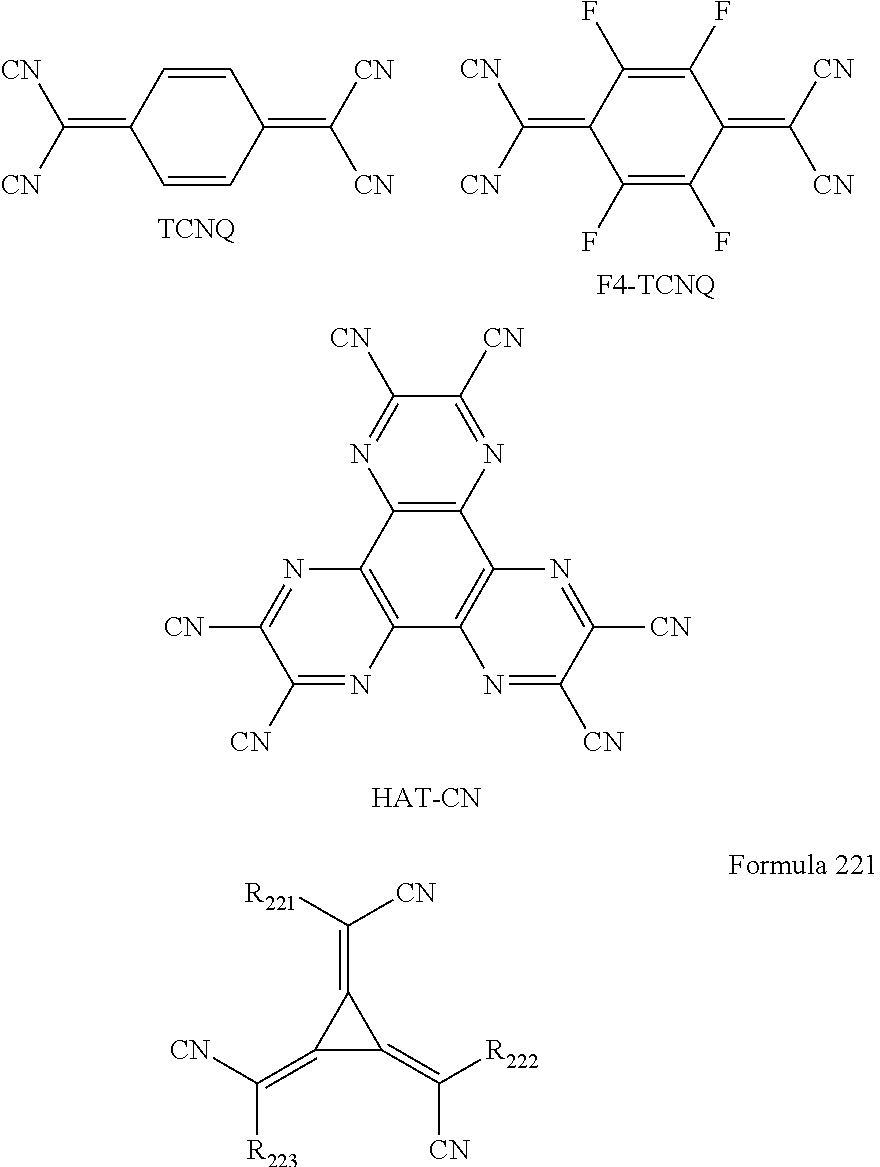
- In Formula 221,
-
- R221 to R223 may each independently be a C3-C60 carbocyclic group that is unsubstituted or substituted with at least one R10a or a C1-C60 heterocyclic group that is unsubstituted or substituted with at least one R10a, and
- at least one of R221 to R223 may each independently be a C3-C60 carbocyclic group or a C1-C60 heterocyclic group, each substituted with: a cyano group; —F; —C1; —Br; —I; a C1-C20 alkyl group that is substituted with a cyano group, —F, —Cl, —Br, —I, or any combination thereof; or any combination thereof.
- In the compound containing the element EL1 and the element EL2, the element EL1 may be metal, metalloid, or a combination thereof, and the element EL2 may be non-metal, metalloid, or a combination thereof.
- Examples of the metal may include an alkali metal (for example, lithium (Li), sodium (Na), potassium (K), rubidium (Rb), cesium (Cs), and/or the like); an alkaline earth metal (for example, beryllium (Be), magnesium (Mg), calcium (Ca), strontium (Sr), barium (Ba), and/or the like); a transition metal (for example, titanium (Ti), zirconium (Zr), hafnium (Hf), vanadium (V), niobium (Nb), tantalum (Ta), chromium (Cr), molybdenum (Mo), tungsten (W), manganese (Mn), technetium (Tc), rhenium (Re), iron (Fe), ruthenium (Ru), osmium (Os), cobalt (Co), rhodium (Rh), iridium (Ir), nickel (Ni), palladium (Pd), platinum (Pt), copper (Cu), silver (Ag), gold (Au), and/or the like); a post-transition metal (for example, zinc (Zn), indium (In), tin (Sn), and/or the like); and a lanthanide metal (for example, lanthanum (La), cerium (Ce), praseodymium (Pr), neodymium (Nd), promethium (Pm), samarium (Sm), europium (Eu), gadolinium (Gd), terbium (Tb), dysprosium (Dy), holmium (Ho), erbium (Er), thulium (Tm), ytterbium (Yb), lutetium (Lu), and/or the like).
- Examples of the metalloid may include silicon (Si), antimony (Sb), and/or tellurium (Te).
- Examples of the non-metal may include oxygen (O) and/or halogen (for example, F, Cl, Br, I, and/or the like).
- Examples of the compound including the element EL1 and the element EL2 may include a metal oxide, a metal halide (for example, a metal fluoride, a metal chloride, a metal bromide, a metal iodide, and/or the like), a metalloid halide (for example, a metalloid fluoride, a metalloid chloride, a metalloid bromide, a metalloid iodide, and/or the like), and a metal telluride, or one or more combinations thereof.
- Examples of the metal oxide may include a tungsten oxide (for example, WO, W2O3, WO2, WO3, W2O5, and/or the like), a vanadium oxide (for example, VO, V2O3, VO2, V2O5, and/or the like), a molybdenum oxide (MoO, Mo2O3, MoO2, MoO3, Mo2O5, and/or the like), and/or a rhenium oxide (for example, ReO3, and/or the like).
- Examples of the metal halide may include an alkali metal halide, an alkaline earth metal halide, a transition metal halide, a post-transition metal halide, and/or a lanthanide metal halide.
- Examples of the alkali metal halide may include LiF, NaF, KF, RbF, CsF, LiCl, NaCl, KCl, RbCl, CsCl, LiBr, NaBr, KBr, RbBr, CsBr, LiI, NaI, KI, RbI, and/or CsI.
- Examples of the alkaline earth metal halide may include BeF2, MgF2, CaF2, SrF2, BaF2, BeCl2, MgCl2, CaCl2), SrCl2, BaCl2, BeBr2, MgBr2, CaBr2, SrBr2, BaBr2, Bel2, Mg12, CaI2, SrI2, and/or BaI2.
- Examples of the transition metal halide may include a titanium halide (for example, TiF4, TiCl4, TiBr4, TiI4, and/or the like), a zirconium halide (for example, ZrF4, ZrCl4, ZrBr4, Zrl4, and/or the like), a hafnium halide (for example, HfF4, HfCl4, HfBr4, Hfl4, and/or the like), a vanadium halide (for example, VF3, VCl3, VBr3, VI3, and/or the like), a niobium halide (for example, NbF3, NbCl3, NbBr3, NbI3, and/or the like), a tantalum halide (for example, TaF3, TaCl3, TaBr3, TaI3, and/or the like), a chromium halide (for example, CrF3, CrCl3, CrBr3, CrI3, and/or the like), a molybdenum halide (for example, MoF3, MoCl3, MoBr3, MoI3, and/or the like), a tungsten halide (for example, WF3, WCl3, WBr3, WI3, and/or the like), a manganese halide (for example, MnF2, MnCl2, MnBr2, MnI2, and/or the like), a technetium halide (for example, TcF2, TcCl2, TcBr2, TcI2, and/or the like), a rhenium halide (for example, ReF2, ReCl2, ReBr2, ReI2, and/or the like), an iron halide (for example, FeF2, FeCl2, FeBr2, FeI2, and/or the like), a ruthenium halide (for example, RuF2, RuCl2, RuBr2, RuI2, and/or the like), an osmium halide (for example, OsF2, OsCl2, OsBr2, OsI2, and/or the like), a cobalt halide (for example, CoF2, CoCl2, CoBr2, CoI2, and/or the like), a rhodium halide (for example, RhF2, RhCl2, RhBr2, RhI2, and/or the like), an iridium halide (for example, IrF2, IrCl2, IrBr2, IrI2, and/or the like), a nickel halide (for example, NiF2, NiCl2, NiBr2, NiI2, and/or the like), a palladium halide (for example, PdF2, PdCl2, PdBr2, PdI2, and/or the like), a platinum halide (for example, PtF2, PtCl2, PtBr2, PtI2, and/or the like), a copper halide (for example, CuF, CuCl, CuBr, CuI, and/or the like), a silver halide (for example, AgF, AgCl, AgBr, AgI, and/or the like), and/or a gold halide (for example, AuF, AuCl, AuBr, AuI, and/or the like).
- Examples of the post-transition metal halide may include a zinc halide (for example, ZnF2, ZnCl2, ZnBr2, ZnI2, and/or the like), an indium halide (for example, InI3, and/or the like), and/or a tin halide (for example, SnI2, and/or the like).
- Examples of the lanthanide metal halide may include YbF, YbF2, YbF3, SmF3, YbCl, YbCl2, YbCl3, SmCl3, YbBr, YbBr2, YbBr3, SmBr3, YbI, YbI2, YbI3, SmI3, and/or the like.
- Examples of the metalloid halide may include an antimony halide (for example, SbCl5, and/or the like).
- Examples of the metal telluride may include an alkali metal telluride (for example, Li2Te, Na2Te, K2Te, Rb2Te, Cs2Te, and/or the like), an alkaline earth metal telluride (for example, BeTe, MgTe, CaTe, SrTe, BaTe, and/or the like), a transition metal telluride (for example, TiTe2, ZrTe2, HfTe2, V2Te3, Nb2Te3, Ta2Te3, Cr2Te3, Mo2Te3, W2Te3, MnTe, TcTe, ReTe, FeTe, RuTe, OsTe, CoTe, RhTe, IrTe, NiTe, PdTe, PtTe, Cu2Te, CuTe, Ag2Te, AgTe, Au2Te, and/or the like), a post-transition metal telluride (for example, ZnTe, and/or the like), and/or a lanthanide metal telluride (for example, LaTe, CeTe, PrTe, NdTe, PmTe, EuTe, GdTe, TbTe, DyTe, HoTe, ErTe, TmTe, YbTe, LuTe, and/or the like).
- When the light-emitting
device 10 is a full-color light-emitting device, the emission layer may be patterned into a red emission layer, a green emission layer, and/or a blue emission layer, according to a sub-pixel. In one or more embodiments, the emission layer may have a stacked structure of two or more layers of a red emission layer, a green emission layer, and a blue emission layer, in which the two or more layers contact each other or are separated from each other, to emit white light. In one or more embodiments, the emission layer may include two or more materials of a red light-emitting material, a green light-emitting material, and a blue light-emitting material, in which the two or more materials are mixed with each other in a single layer, to emit white light. - In one or more embodiments, the emission layer may include a host and a dopant (or emitter). In one or more embodiments, the emission layer may further include an auxiliary dopant that promotes energy transfer to a dopant (or emitter), in addition to the host and the dopant (or emitter). When the emission layer includes the dopant (or emitter) and the auxiliary dopant, the dopant (or emitter) and the auxiliary dopant are different from each other.
- The organometallic compound represented by Formula 1 may act as the dopant (or emitter), or may act as the auxiliary dopant.
- The amount (weight) of the dopant (or emitter) in the emission layer may be about 0.01 parts by weight to about 15 parts by weight based on 100 parts by weight of the host.
- The emission layer may include the organometallic compound represented by Formula 1. The amount (weight) of the organometallic compound in the emission layer may be about 0.01 parts by weight to about 30 parts by weight, about 0.1 parts by weight to about 20 parts by weight, or about 0.1 parts by weight to about 15 parts by weight, based on 100 parts by weight of the emission layer.
- The thickness of the emission layer may be about 100 Å to about 1,000 Å, for example, about 200 Å to about 600 Å. When the thickness of the emission layer is within the range, excellent or suitable light-emission characteristics may be obtained without a substantial increase in driving voltage.
- The host in the emission layer may include the second compound or the third compound described herein, or any combination thereof.
- In one or more embodiments, the host may include a compound represented by Formula 301.
-
[Ar301]xb11-[(L301)xb1-R301]xb21 Formula 301 - In Formula 301,
-
- Ar301 and L301 may each independently be a C3-C60 carbocyclic group that is unsubstituted or substituted with at least one R10a or a C1-C60 heterocyclic group that is unsubstituted or substituted with at least one R10a,
- xb11 may be 1, 2, or 3,
- xb1 may be an integer from 0 to 5,
- R301 may be hydrogen, deuterium, —F, —Cl, —Br, —I, a hydroxyl group, a cyano group, a nitro group, a C1-C60 alkyl group that is unsubstituted or substituted with at least one R10a, a C2-C60 alkenyl group that is unsubstituted or substituted with at least one R10a, a C2-C60 alkynyl group that is unsubstituted or substituted with at least one R10a, a C1-C60 alkoxy group that is unsubstituted or substituted with at least one R10a, a C3-C60 carbocyclic group that is unsubstituted or substituted with at least one R10a, a C1-C60 heterocyclic group that is unsubstituted or substituted with at least one R10a, —Si(Q301)(Q302)(Q303), —N(Q301)(Q302), —B(Q301)(Q302), —C(═O)(Q301), —S(═O)2(Q301), or —P(═O)(Q301)(Q302),
- xb21 may be an integer from 1 to 5, and
- Q301 to Q303 are each as described in connection with Q1.
- In one or more embodiments, when xb11 in Formula 301 is 2 or more, two or more of Ar301 may be linked to each other via a single bond.
- In one or more embodiments, the host may include at least one compound represented by Formula 301-1, at least one compound represented by Formula 301-2, or any combination thereof:
-

-
- wherein, in Formulae 301-1 and 301-2,
- ring A301 to ring A304 may each independently be a C3-C60 carbocyclic group that is unsubstituted or substituted with at least one R10a or a C1-C60 heterocyclic group that is unsubstituted or substituted with at least one R10a,
- X301 may be O, S, N-[(L304)xb4-R304], C(R304)(R305), or Si(R304)(R305),
- xb22 and xb23 may each independently be 0, 1, or 2,
- L301, xb1, and R301 are each as described herein,
- L302 to L304 may each independently be as described in connection with L301, xb2 to xb4 may each independently be as described in connection with xb1, and
- R302 to R305 and R311 to R314 are each as described in connection with R301.
- In one or more embodiments, the host may include an alkali earth metal complex, a post-transition metal complex, or any combination thereof. In one or more embodiments, the host may include a Be complex (for example, Compound H55), an Mg complex, a Zn complex, or any combination thereof.
- In one or more embodiments, the host may include at least one selected from among Compounds H1 to H130, 9,10-di(2-naphthyl)anthracene (ADN), 2-methyl-9,10-bis(naphthalen-2-yl)anthracene (MADN), 9,10-di(2-naphthyl)-2-t-butyl-anthracene (TBADN), 4,4′-bis(N-carbazolyl)-1,1′-biphenyl (CBP), 1,3-di-9-carbazolylbenzene (mCP), 1,3,5-tri(carbazol-9-yl)benzene (TCP), and/or any combination thereof:
-
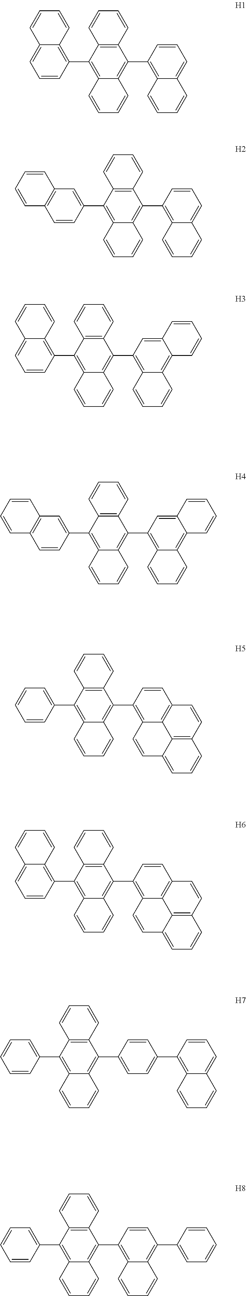
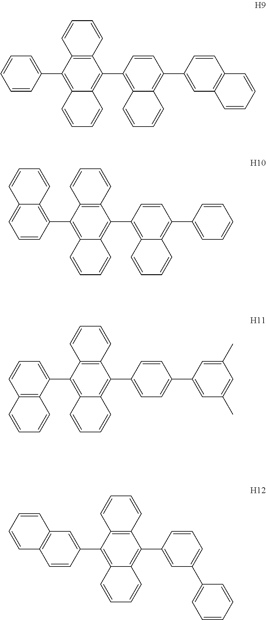
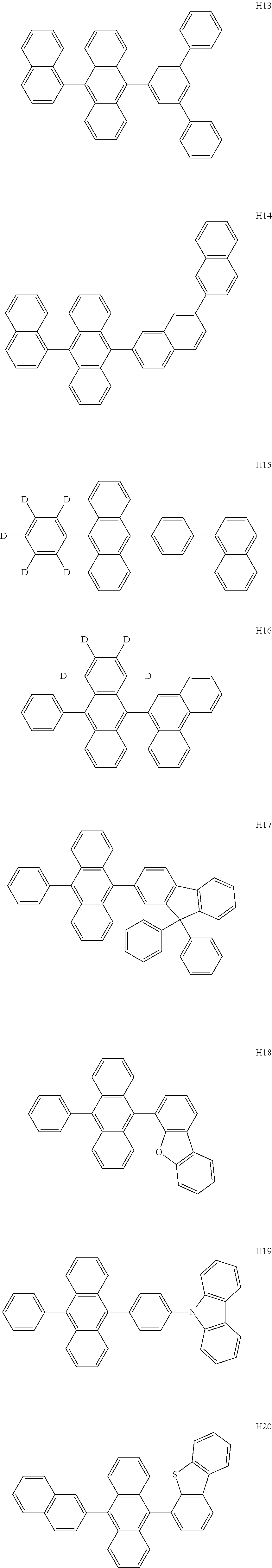
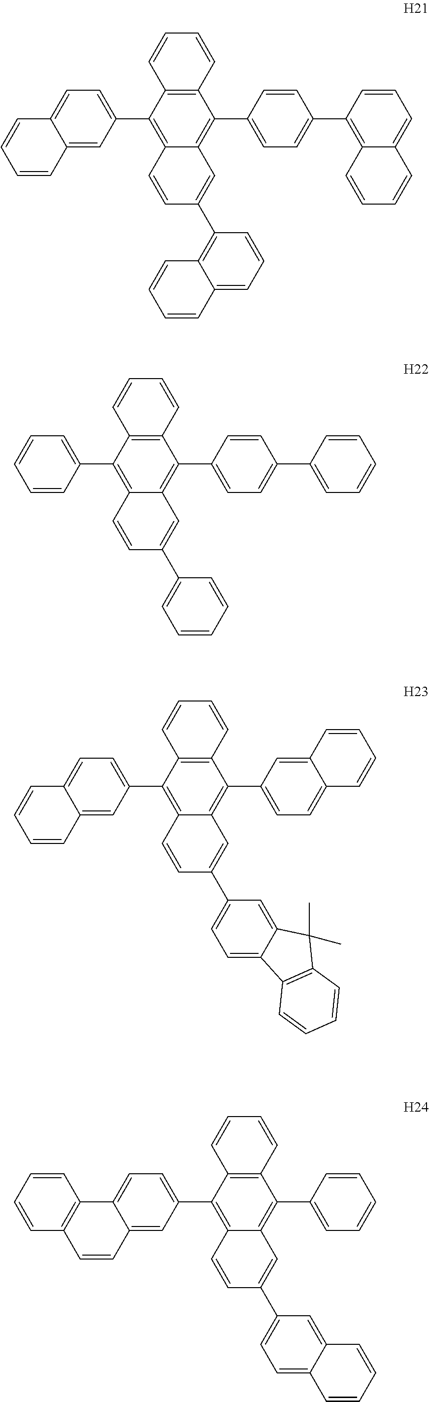
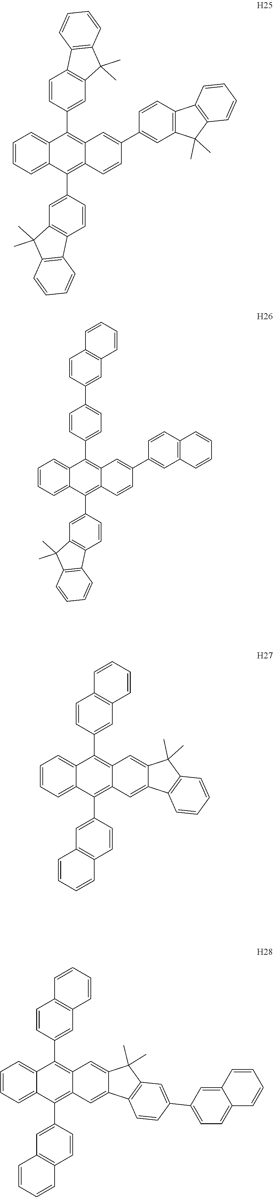
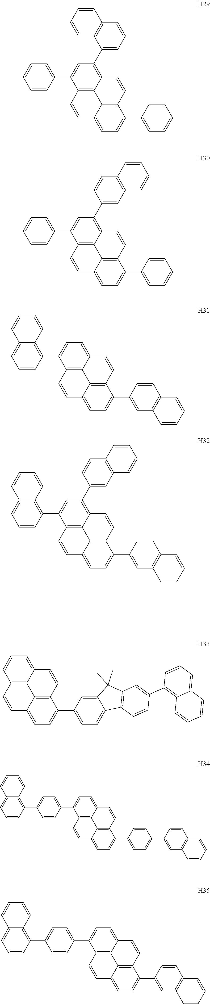


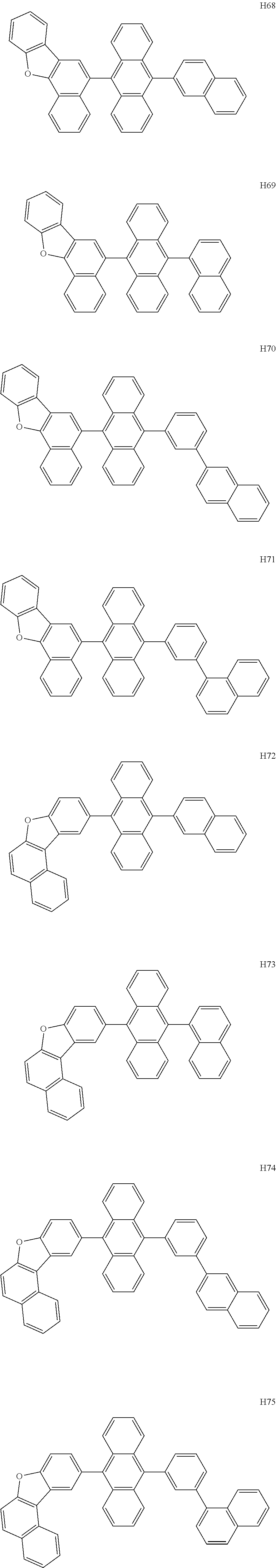
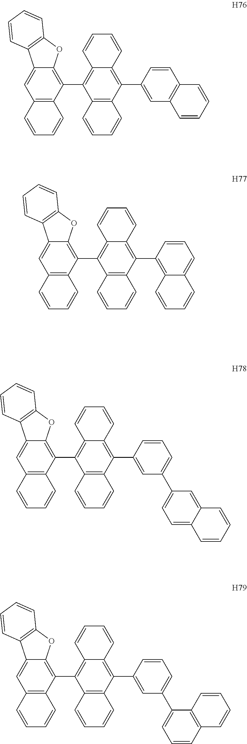
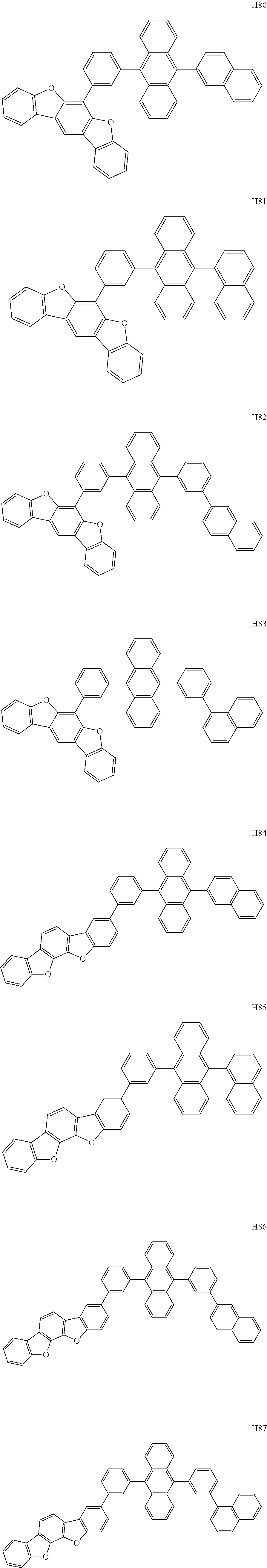
-


- In one or more embodiments, the host may include a silicon-containing compound, a phosphine oxide-containing compound, or any combination thereof.
- The host may have one or more suitable modifications. For example, the host may include only one kind of compound, or may include two or more kinds of different compounds.
- The emission layer may include, as a phosphorescent dopant, the organometallic compound represented by Formula 1 as described herein.
- In one or more embodiments, when the emission layer includes the organometallic compound represented by Formula 1 as described herein, and the organometallic compound represented by Formula 1 as described herein acts as an auxiliary dopant, the emission layer may include a phosphorescent dopant.
- The phosphorescent dopant may include at least one transition metal as a central metal.
- The phosphorescent dopant may include a monodentate ligand, a bidentate ligand, a tridentate ligand, a tetradentate ligand, a pentadentate ligand, a hexadentate ligand, or a (e.g., any) combination thereof.
- The phosphorescent dopant may be electrically neutral.
- In one or more embodiments, the phosphorescent dopant may include at least one organometallic compound represented by Formula 401:
-

-
- wherein, in Formulae 401 and 402,
- M may be a transition metal (for example, iridium (Ir), platinum (Pt), palladium (Pd), osmium (Os), titanium (Ti), gold (Au), hafnium (Hf), europium (Eu), terbium (Tb), rhodium (Rh), rhenium (Re), or thulium (Tm)),
- L401 may be a ligand represented by Formula 402, and xc1 may be 1, 2, or 3, wherein, when xc1 is 2 or more, two or more of L401 may be identical to or different from each other,
- L402 may be an organic ligand, and xc2 may be 0, 1, 2, 3, or 4, wherein, when xc2 is 2 or more, two or more of L402 may be identical to or different from each other,
- X401 and X402 may each independently be nitrogen or carbon,
- ring A401 and ring A402 may each independently be a C3-C60 carbocyclic group or a C1-C60 heterocyclic group,
- T401 may be a single bond, *—O—*′, *—S—, *—C(═O)—*′, *—N(Q411)-*′, *—C(Q411)(Q412)-*′, *—C(Q411)=C(Q412)-*′, *—C(Q411)=*′, or *═C═*′, * and *′ each indicate a binding site to a neighboring atom,
- X403 and X404 may each independently be a chemical bond (for example, a covalent bond or a coordinate bond), O, S, N(Q413), B(Q413), P(Q413), C(Q413)(Q414), or Si(Q413) (Q414),
- Q411 to Q414 are each as described in connection with Q1,
- R401 and R402 may each independently be hydrogen, deuterium, —F, —Cl, —Br, —I, a hydroxyl group, a cyano group, a nitro group, a C1-C20 alkyl group that is unsubstituted or substituted with at least one R10a, a C1-C20 alkoxy group that is unsubstituted or substituted with at least one R10a, a C3-C60 carbocyclic group that is unsubstituted or substituted with at least one R10a, a C1-C60 heterocyclic group that is unsubstituted or substituted with at least one R10a, —Si(Q401)(Q402)(Q403), —N(Q401)(Q402), —B(Q401)(Q402), —C(═O)(Q401), —S(═O)2(Q401), or —P(═O)(Q401)(Q402),
- Q401 to Q403 are each as described in connection with Q1,
- xc11 and xc12 may each independently be an integer from 0 to 10, and
- * and *′ in Formula 402 may each indicate a binding site to M in Formula 401.
- In one or more embodiments, in Formula 402, i) X401 may be nitrogen, and X402 may be carbon, or ii) each of X401 and X402 may be nitrogen.
- In one or more embodiments, when xc1 in Formula 401 is 2 or more, two ring A401 in two or more selected from L401 may be optionally linked to each other via T402, which is a linking group, or two ring A402 may optionally be linked to each other via T403, which is a linking group (see Compounds PD1 to PD4 and PD7). T402 and T403 are each as described in connection with T401.
- L402 in Formula 401 may be an organic ligand. In one or more embodiments, L402 may include a halogen group, a diketone group (for example, an acetylacetonate group), a carboxylic acid group (for example, a picolinate group), —C(═O), an isonitrile group, a —CN, a phosphorus-containing group (for example, a phosphine group, a phosphite group, and/or the like), or any combination thereof.
- The phosphorescent dopant may include, for example, at least one of Compounds PD1 to PD25, or a (e.g., any) combination thereof:
-
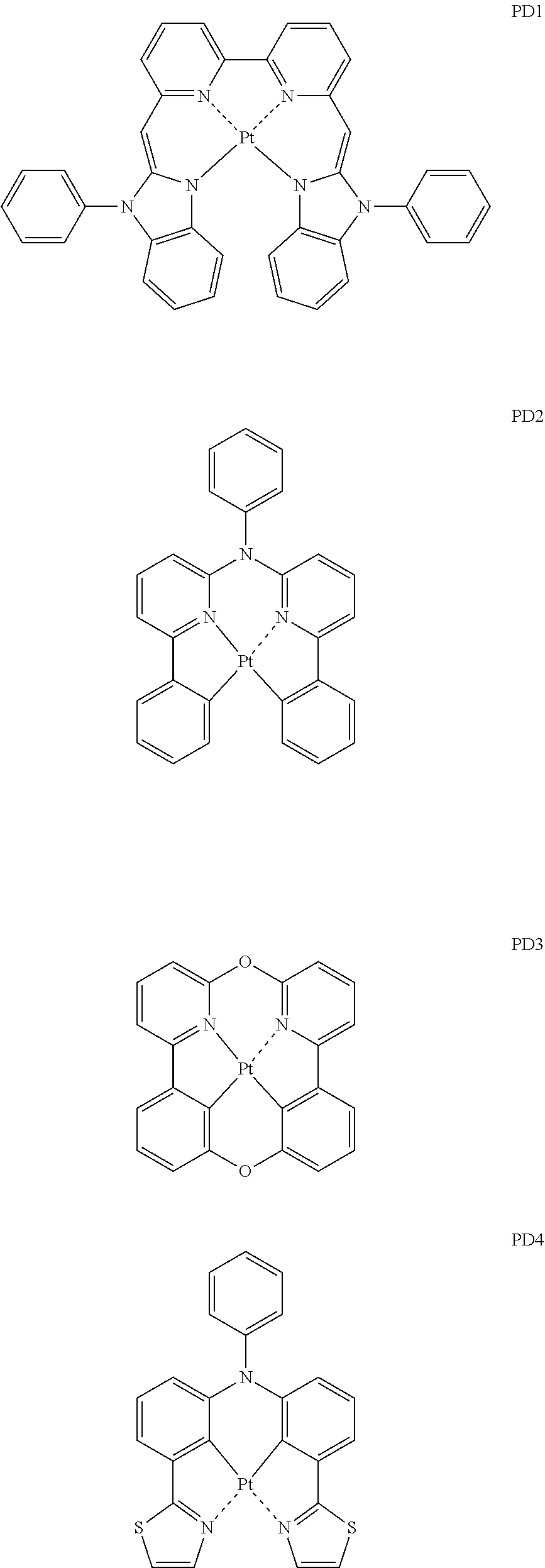
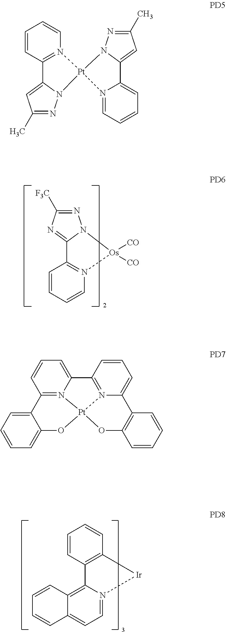
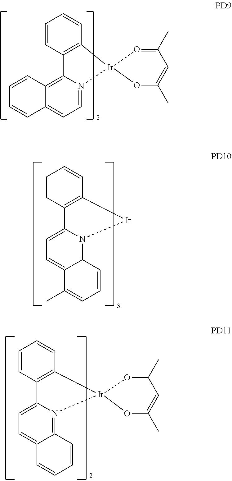

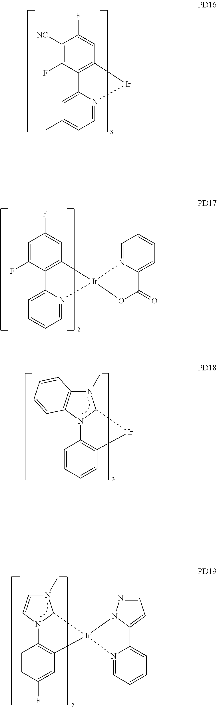
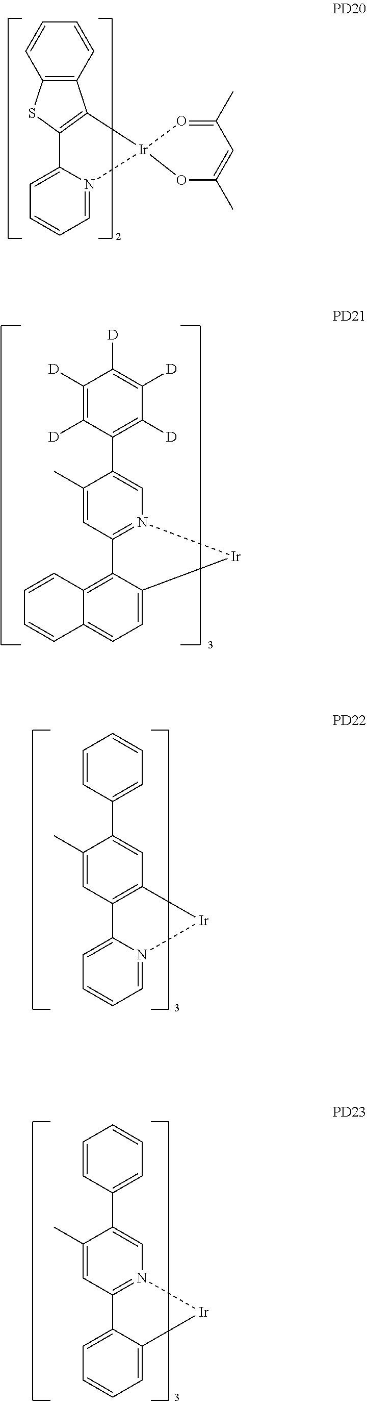
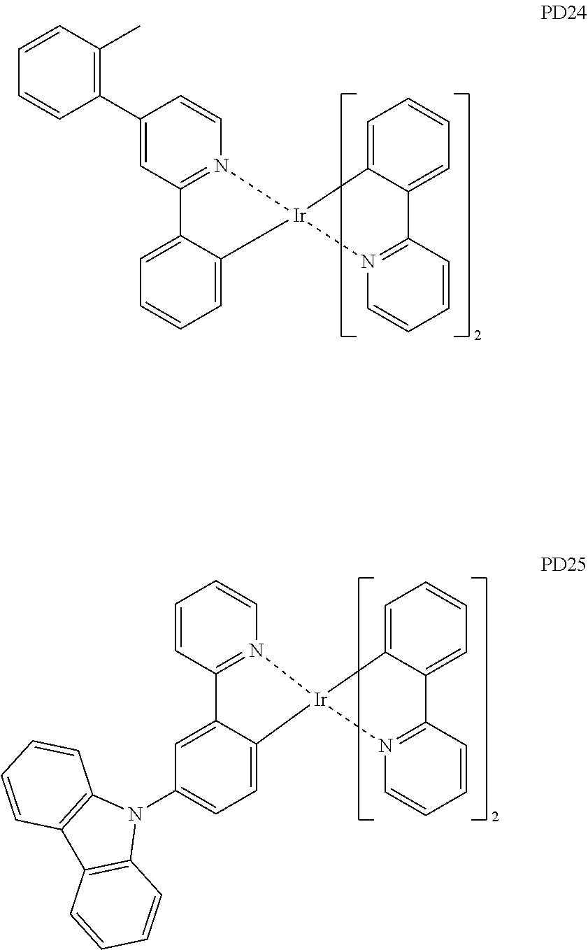
- When the emission layer includes the organometallic compound represented by Formula 1 as described herein, and the organometallic compound represented by Formula 1 as described herein acts as an auxiliary dopant, the emission layer may further include a fluorescent dopant.
- In one or more embodiments, when the emission layer includes the organometallic compound represented by Formula 1 as described herein, and the organometallic compound represented by Formula 1 as described herein acts as a phosphorescent dopant, the emission layer may further include an auxiliary dopant.
- The fluorescent dopant and the auxiliary dopant may each independently include an arylamine compound, a styrylamine compound, a boron-containing compound, or any combination thereof.
- In one or more embodiments, the fluorescent dopant and the auxiliary dopant may each independently include a compound represented by Formula 501:
-

-
- wherein, in Formula 501,
- Ar501, L501 to L503, R501, and R502 may each independently be a C3-C60 carbocyclic group that is unsubstituted or substituted with at least one R10a or a C1-C60 heterocyclic group that is unsubstituted or substituted with at least one R10a,
- xd1 to xd3 may each independently be 0, 1, 2, or 3, and
- xd4 may be 1, 2, 3, 4, 5, or 6.
- In one or more embodiments, Ar501 in Formula 501 may be a condensed cyclic group (for example, an anthracene group, a chrysene group, a pyrene group, and/or the like) in which three or more monocyclic groups are condensed together.
- In one or more embodiments, xd4 in Formula 501 may be 2.
- In one or more embodiments, the fluorescent dopant and the auxiliary dopant may each include at least one of Compounds FD1 to FD36, DPVBi, DPAVBi, and/or any combination thereof:
-
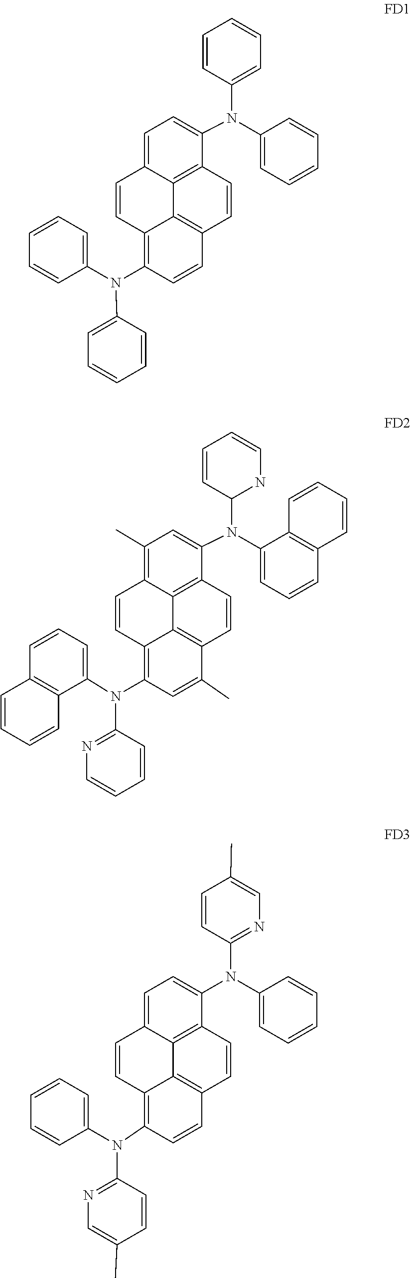
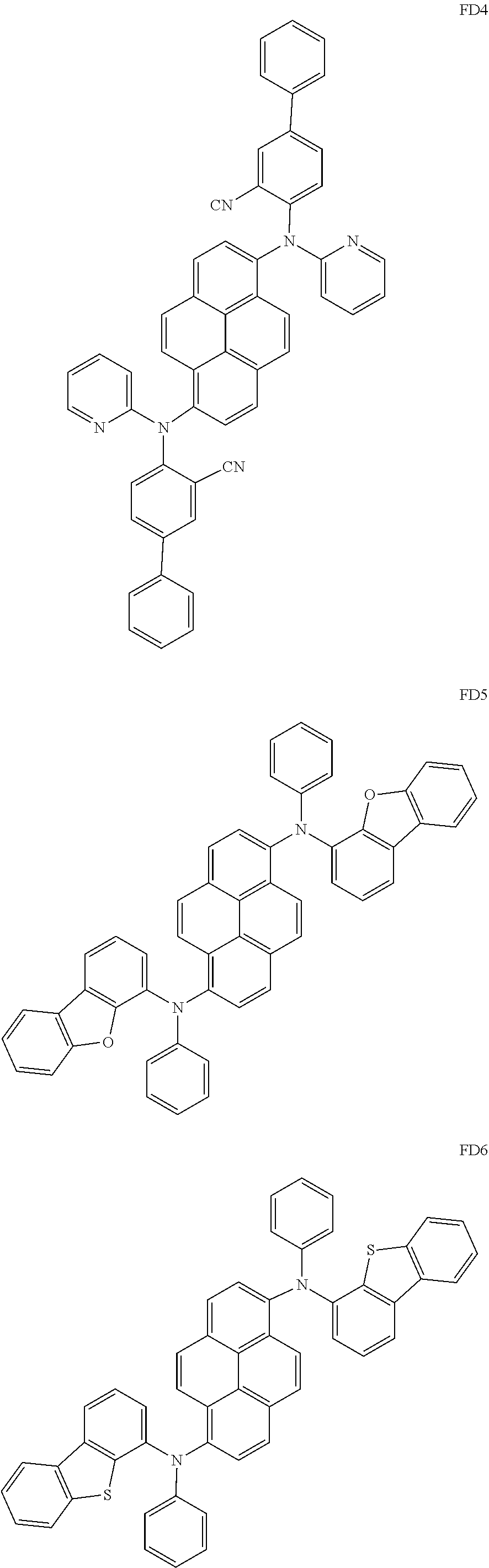
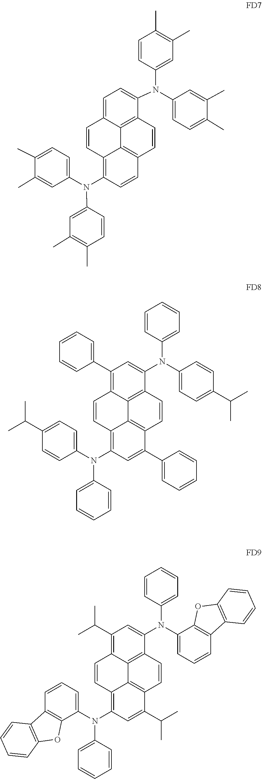
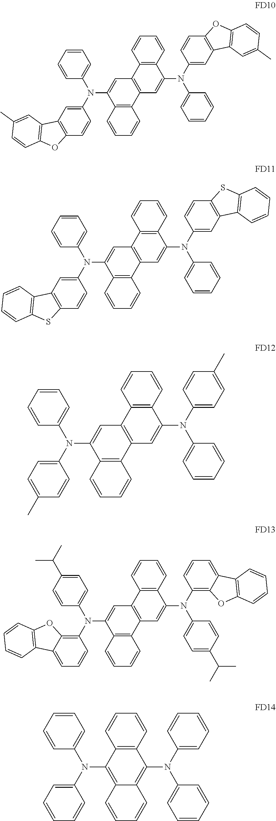
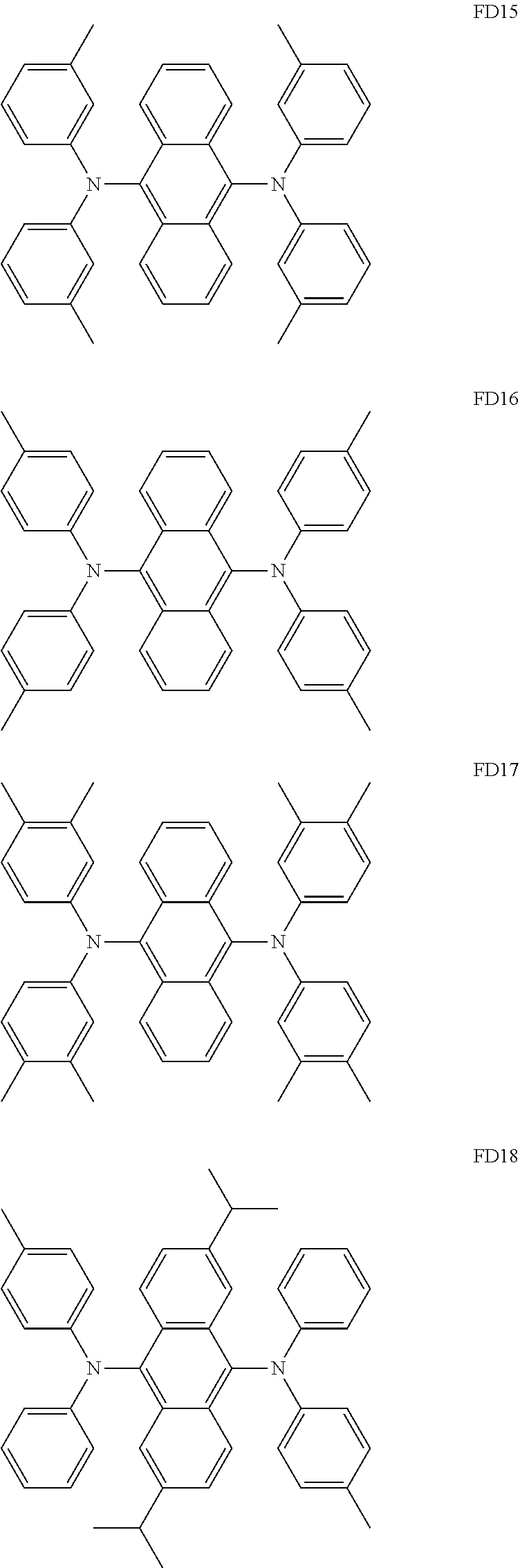


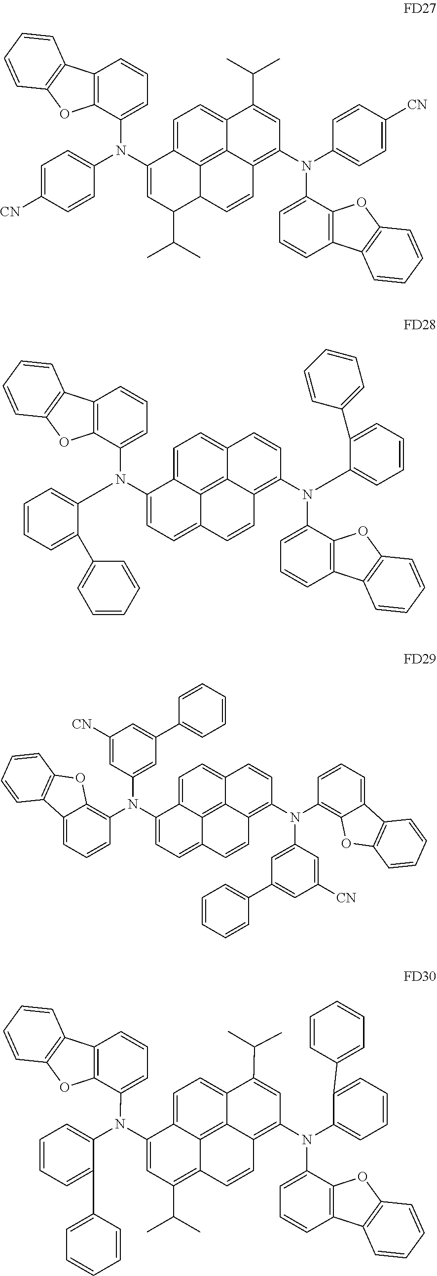
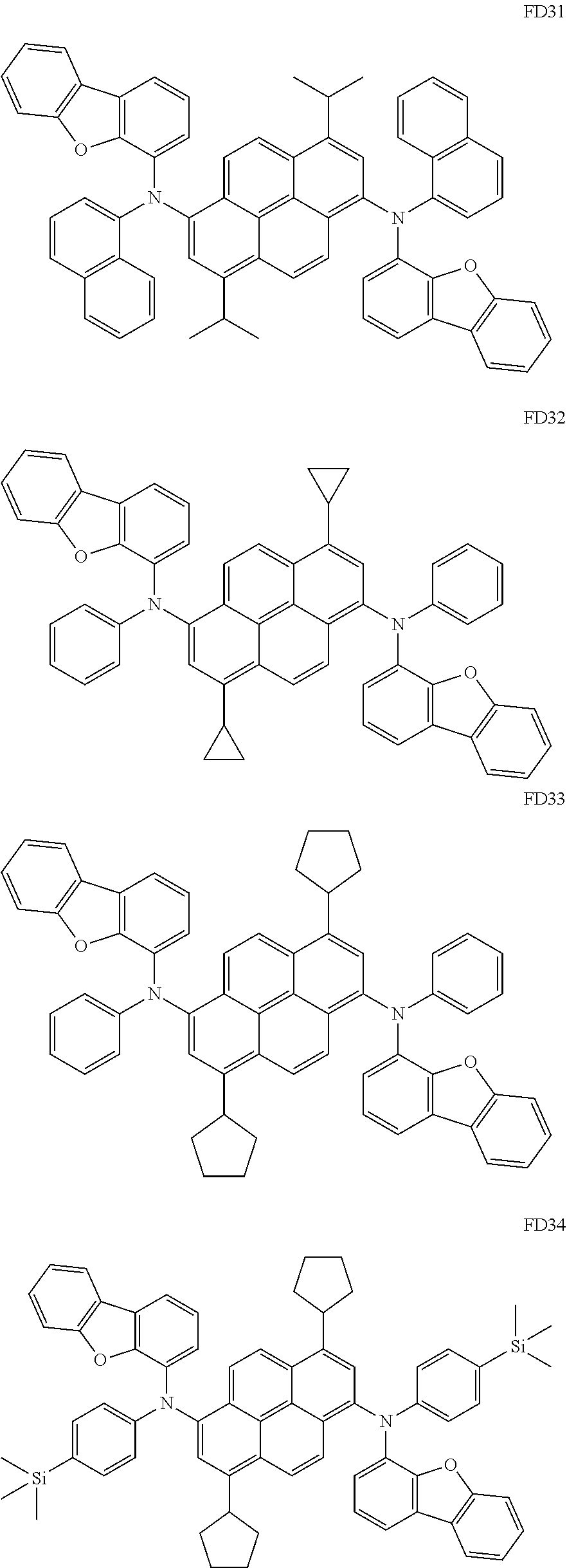
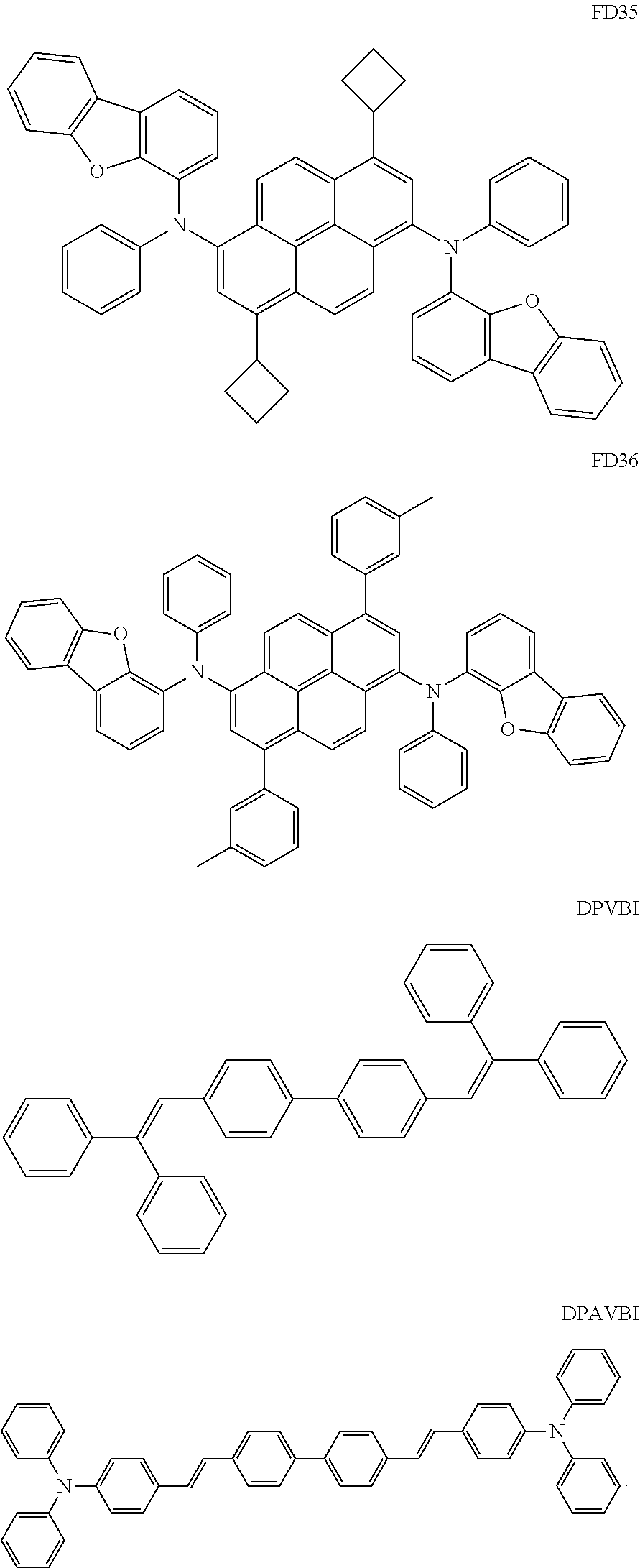
- In one or more embodiments, the fluorescent dopant and the auxiliary dopant may each independently include a fourth compound represented by Formula 502 or 503 as described herein.
- The electron transport region may have: i) a single-layered structure including (e.g., consisting of) a single layer including (e.g., consisting of) a single material, ii) a single-layered structure including (e.g., consisting of) a single layer including multiple different materials, or iii) a multilayer structure including multiple layers including multiple different materials.
- The electron transport region may include a buffer layer, a hole blocking layer, an electron control layer, an electron transport layer, an electron injection layer, or any combination thereof.
- In one or more embodiments, the electron transport region may have an electron transport layer/electron injection layer structure, a hole blocking layer/electron transport layer/electron injection layer structure, an electron control layer/electron transport layer/electron injection layer structure, or a buffer layer/electron transport layer/electron injection layer structure, wherein constituent layers of each structure are stacked in the stated order from the emission layer.
- The electron transport region (for example, the buffer layer, the hole blocking layer, the electron control layer, or the electron transport layer in the electron transport region) may include a metal-free compound including at least one π electron-deficient nitrogen-containing C1-C60 heterocyclic group.
- In one or more embodiments, the electron transport region may include a compound represented by Formula 601.
-
[Ar601]xe11-[(L601)xe1-R601]xe21 Formula 601 - In Formula 601,
-
- Ar601 and L601 may each independently be a C3-C60 carbocyclic group that is unsubstituted or substituted with at least one R10a or a C1-C60 heterocyclic group that is unsubstituted or substituted with at least one R10a,
- xe11 may be 1, 2, or 3,
- xe1 may be 0, 1, 2, 3, 4, or 5,
- R601 may be a C3-C60 carbocyclic group that is unsubstituted or substituted with at least one R10a, a C1-C60 heterocyclic group that is unsubstituted or substituted with at least one R10a, —Si(Q601)(Q602)(Q603), —C(═O)(Q601), —S(═O)2(Q601), or —P(═O)(Q601)(Q602),
- Q601 to Q603 are each as described in connection with Q1,
- xe21 may be 1, 2, 3, 4, or 5, and
- at least one of Ar601, L601, and R601 may each independently be a π electron-deficient nitrogen-containing C1-C60 heterocyclic group that is unsubstituted or substituted with at least one R10a.
- In one or more embodiments, when xe11 in Formula 601 is 2 or more, two or more of Ar601 may be linked together via a single bond.
- In one or more embodiments, Ar601 in Formula 601 may be an anthracene group that is unsubstituted or substituted with at least one R10a.
- In one or more embodiments, the electron transport region may include a compound represented by Formula 601-1:
-
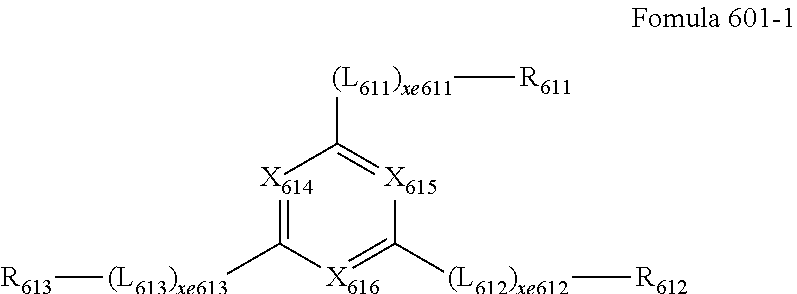
- wherein, in Formula 601-1,
-
- X614 may be N or C(R614), X615 may be N or C(R615), X616 may be N or C(R616), and at least one of X614 to X616 may be N,
- L611 to L613 are each as described in connection with L601,
- xe611 to xe613 are each as described in connection with xe1,
- R611 to R613 are each as described in connection with R601, and
- R614 to R616 may each independently be hydrogen, deuterium, —F, —Cl, —Br, —I, a hydroxyl group, a cyano group, a nitro group, a C1-C20 alkyl group, a C1-C20 alkoxy group, a C3-C60 carbocyclic group that is unsubstituted or substituted with at least one R10a, or a C1-C60 heterocyclic group that is unsubstituted or substituted with at least one R10a.
- In one or more embodiments, xe1 and xe611 to xe613 in Formulae 601 and 601-1 may each independently be 0, 1, or 2.
- The electron transport region may include at least one selected from among Compounds ET1 to ET46, 2,9-dimethyl-4,7-diphenyl-1,10-phenanthroline (BOP), 4,7-diphenyl-1,10-phenanthroline (Bphen), Alq3, BAlq, TAZ, NTAZ, and/or any combination thereof:
-
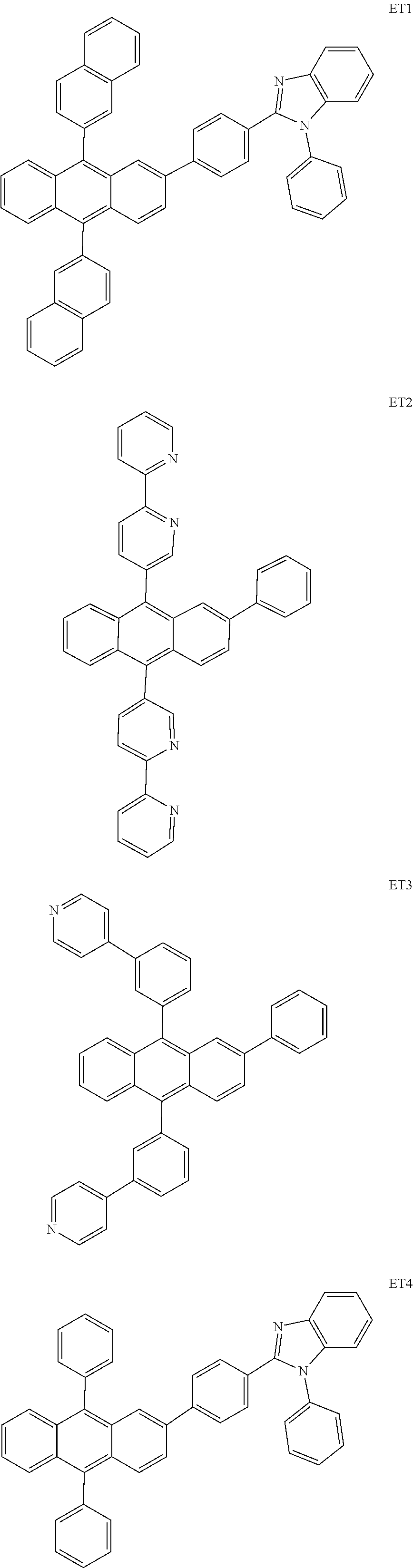
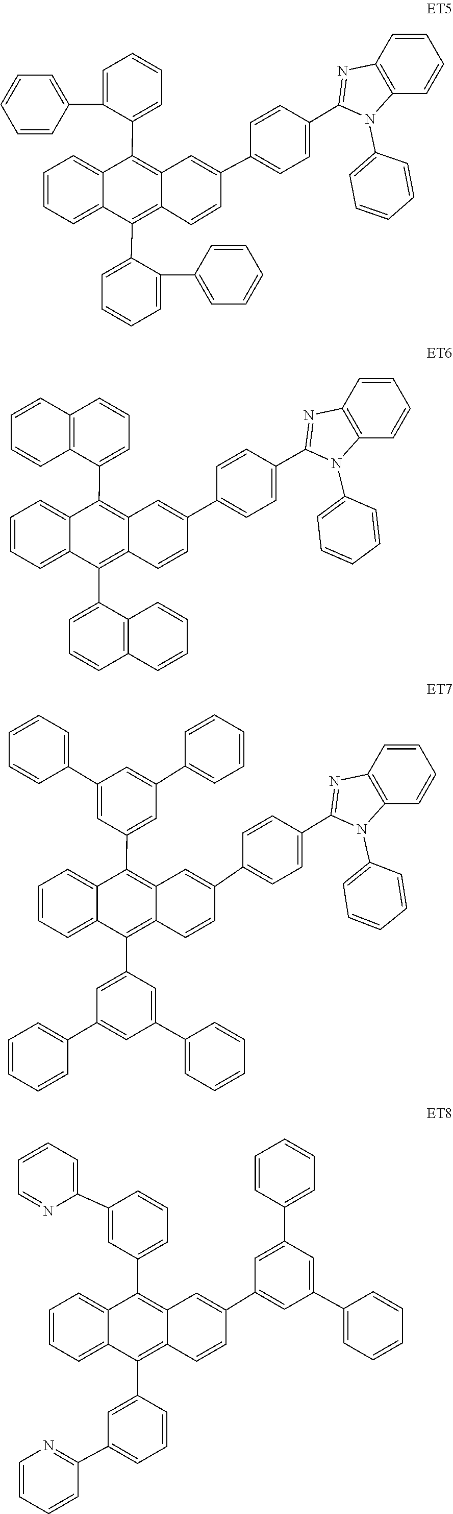
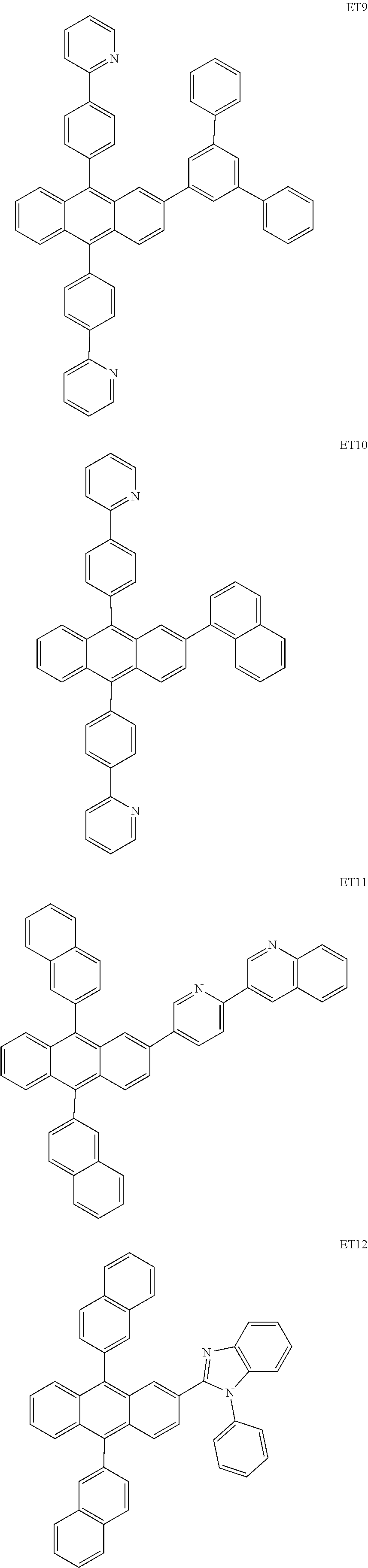


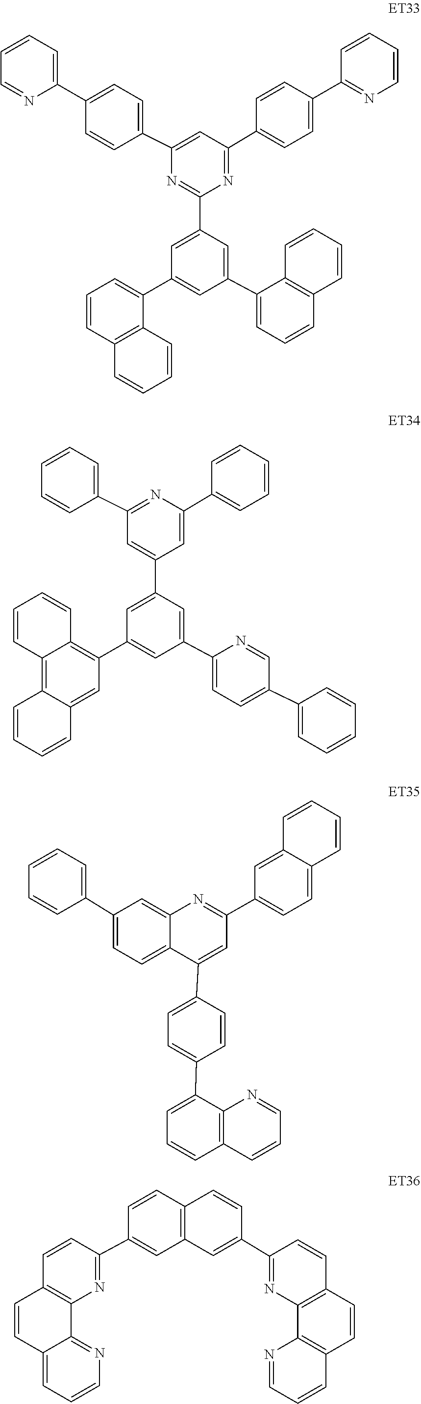
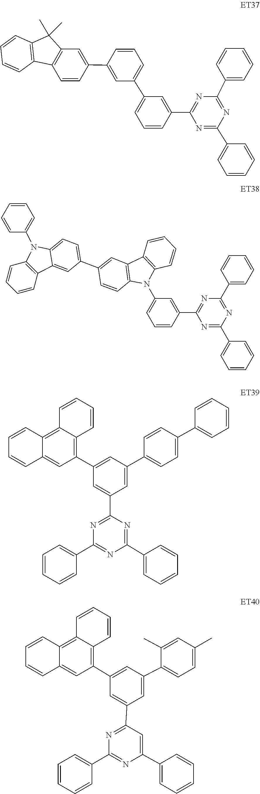
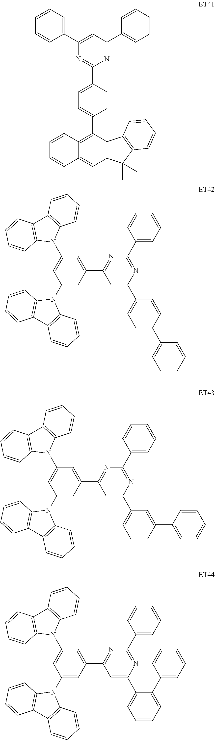
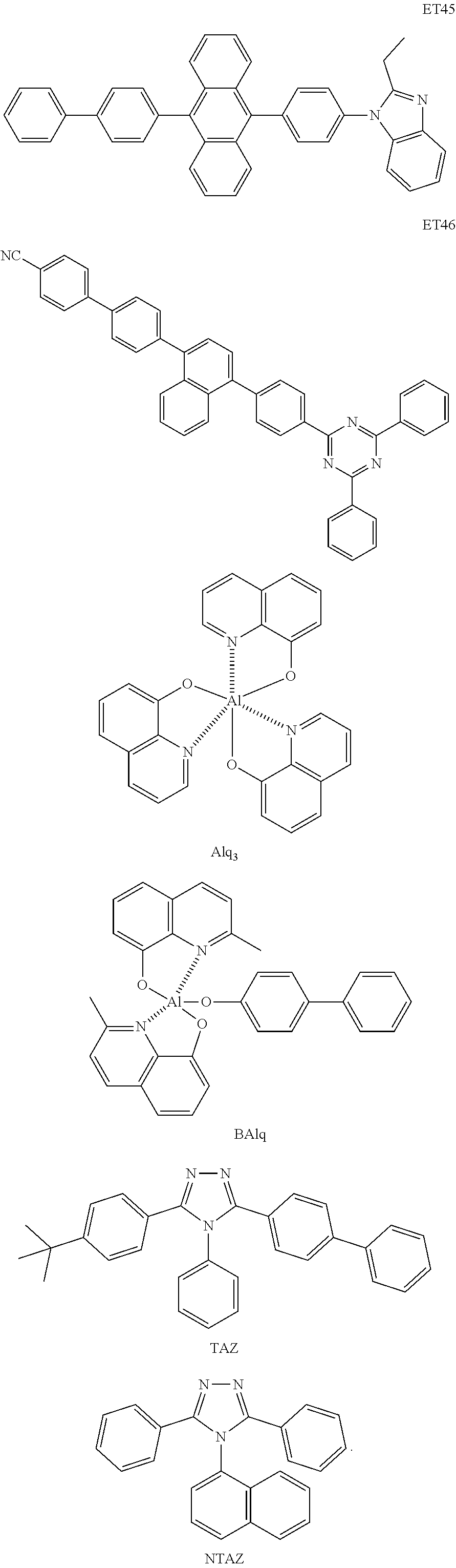
- The thickness of the electron transport region may be about 100 Å to about 5,000 Å, for example, about 160 Å to about 4,000 Å. When the electron transport region includes a buffer layer, a hole blocking layer, an electron control layer, an electron transport layer, or any combination thereof, the thickness of the buffer layer, the hole blocking layer, or the electron control layer may each independently be from about 20 Å to about 1,000 Å, for example, about 30 Å to about 300 Å, and the thickness of the electron transport layer may be from about 100 Å to about 1,000 Å, for example, about 150 Å to about 500 Å. When the thicknesses of the buffer layer, the hole blocking layer, the electron control layer, the electron transport layer, and/or the electron transport layer are within these ranges, satisfactory electron-transporting characteristics may be obtained without a substantial increase in driving voltage.
- The electron transport region (for example, the electron transport layer in the electron transport region) may further include, in addition to the materials described herein, a metal-containing material.
- The metal-containing material may include an alkali metal complex, an alkaline earth metal complex, or any combination thereof. A metal ion of the alkali metal complex may be a Li ion, a Na ion, a K ion, a Rb ion, or a Cs ion, and a metal ion of the alkaline earth metal complex may be a Be ion, a Mg ion, a Ca ion, a Sr ion, or a Ba ion. A ligand coordinated with the metal ion of the alkali metal complex or the alkaline earth-metal complex may include at least one selected from among a hydroxyquinoline, a hydroxyisoquinoline, a hydroxybenzoquinoline, a hydroxyacridine, a hydroxyphenanthridine, a hydroxyphenyloxazole, a hydroxyphenylthiazole, a hydroxyphenyloxadiazole, a hydroxyphenylthiadiazole, a hydroxyphenylpyridine, a hydroxyphenylbenzimidazole, a hydroxyphenylbenzothiazole, a bipyridine, a phenanthroline, a cyclopentadiene, and/or any combination thereof.
- In one or more embodiments, the metal-containing material may include a Li complex. The Li complex may include, for example, Compound ET-D1 (LiQ) and/or ET-D2:
-
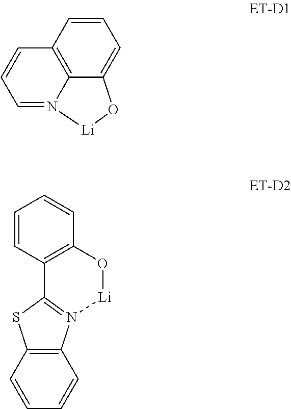
- The electron transport region may include an electron injection layer that facilitates the injection of electrons from the
second electrode 150. The electron injection layer may directly contact thesecond electrode 150. - The electron injection layer may have: i) a single-layered structure including (e.g., consisting of) a single layer including (e.g., consisting of) a single material, ii) a single-layered structure including (e.g., consisting of) a single layer including multiple different materials, or iii) a multilayer structure including multiple layers including multiple different materials.
- The electron injection layer may include an alkali metal, an alkaline earth metal, a rare earth metal, an alkali metal-containing compound, an alkaline earth metal-containing compound, a rare earth metal-containing compound, an alkali metal complex, an alkaline earth metal complex, a rare earth metal complex, or any combination thereof.
- The alkali metal may include Li, Na, K, Rb, Cs, or any combination thereof. The alkaline earth metal may include Mg, Ca, Sr, Ba, or any combination thereof. The rare earth metal may include Sc, Y, Ce, Tb, Yb, Gd, or any combination thereof.
- The alkali metal-containing compound, the alkaline earth metal-containing compound, and the rare earth metal-containing compound may include oxides, halides (for example, fluorides, chlorides, bromides, iodides, and/or the like), or tellurides of the alkali metal, the alkaline earth metal, and the rare earth metal, and/or any combination thereof.
- The alkali metal-containing compound may include: alkali metal oxides, such as Li2O, Cs2O, or K2O; alkali metal halides, such as LiF, NaF, CsF, KF, LiI, NaI, CsI, KI, or RbI; or any combination thereof. The alkaline earth metal-containing compound may include an alkaline earth metal oxide, such as BaO, SrO, CaO, BaxSr1-xO (x is a real number satisfying 0<x<1), or BaxCa1-xO (x is a real number satisfying 0<x<1). The rare earth metal-containing compound may include YbF3, ScF3, Sc2O3, Y2O3, Ce2O3, GdF3, TbF3, YbI3, ScI3, TbI3, or any combination thereof. In one or more embodiments, the rare earth metal-containing compound may include a lanthanide metal telluride. Examples of the lanthanide metal telluride may include LaTe, CeTe, PrTe, NdTe, PmTe, SmTe, EuTe, GdTe, TbTe, DyTe, HoTe, ErTe, TmTe, YbTe, LuTe, La2Te3, Ce2Te3, Pr2Te3, Nd2Te3, Pm2Te3, Sm2Te3, Eu2Te3, Gd2Te3, Tb2Te3, Dy2Te3, Ho2Te3, Er2Te3, Tm2Te3, Yb2Te3, and/or Lu2Te3.
- The alkali metal complex, the alkaline earth-metal complex, and the rare earth metal complex may include i) one selected from among metal ions of the alkali metal, the alkaline earth metal, and the rare earth metal and ii), a ligand bonded to the metal ion (e.g., the selected metal ion), for example, a hydroxyquinoline, a hydroxyisoquinoline, a hydroxybenzoquinoline, a hydroxyacridine, a hydroxyphenanthridine, a hydroxyphenyloxazole, a hydroxyphenylthiazole, a hydroxyphenyloxadiazole, a hydroxyphenylthiadiazole, a hydroxyphenylpyridine, a hydroxyphenyl benzimidazole, a hydroxyphenylbenzothiazole, a bipyridine, a phenanthroline, a cyclopentadiene, and/or any combination thereof.
- The electron injection layer may include (e.g., consist of) an alkali metal, an alkaline earth metal, a rare earth metal, an alkali metal-containing compound, an alkaline earth metal-containing compound, a rare earth metal-containing compound, an alkali metal complex, an alkaline earth metal complex, a rare earth metal complex, or any combination thereof, as described herein. In one or more embodiments, the electron injection layer may further include an organic material (for example, a compound represented by Formula 601).
- In one or more embodiments, the electron injection layer may include (e.g., consist of) i) an alkali metal-containing compound (for example, alkali metal halide), ii) a) an alkali metal-containing compound (for example, alkali metal halide); and b) an alkali metal, an alkaline earth metal, a rare earth metal, or any combination thereof. In one or more embodiments, the electron injection layer may be a KI:Yb co-deposited layer, an RbI:Yb co-deposited layer, a LiF:Yb co-deposited layer, and/or the like.
- When the electron injection layer further includes an organic material, the alkali metal, the alkaline earth metal, the rare earth metal, the alkali metal-containing compound, the alkaline earth metal-containing compound, the rare earth metal-containing compound, the alkali metal complex, the alkaline earth-metal complex, the rare earth metal complex, or any combination thereof may be uniformly or non-uniformly dispersed in a matrix including the organic material.
- The thickness of the electron injection layer may be about 1 Å to about 100 Å, and, for example, about 3 Å to about 90 Å. When the thickness of the electron injection layer is within the range as described herein, satisfactory electron injection characteristics may be obtained without a substantial increase in driving voltage.
- The
second electrode 150 is arranged on theinterlayer 130. Thesecond electrode 150 may be a cathode, which is an electron injection electrode, and as a material for forming thesecond electrode 150, a metal, an alloy, an electrically conductive compound, or any combination thereof, each having a low-work function, may be utilized. - The
second electrode 150 may include lithium (Li), silver (Ag), magnesium (Mg), aluminum (Al), aluminum-lithium (Al—Li), calcium (Ca), magnesium-indium (Mg—In), magnesium-silver (Mg—Ag), ytterbium (Yb), silver-ytterbium (Ag—Yb), ITO, IZO, or any combination thereof. Thesecond electrode 150 may be a transmissive electrode, a semi-transmissive electrode, or a reflective electrode. - The
second electrode 150 may have a single-layer structure or a multilayer structure including a plurality of layers. - The first capping layer may be arranged outside (and e.g., on) the
first electrode 110, and/or the second capping layer may be arranged outside (and e.g., on) thesecond electrode 150. In detail, the light-emittingdevice 10 may have a structure in which the first capping layer, thefirst electrode 110, theinterlayer 130, and thesecond electrode 150 are sequentially stacked in this stated order, a structure in which thefirst electrode 110, theinterlayer 130, thesecond electrode 150, and the second capping layer are sequentially stacked in this stated order, or a structure in which the first capping layer, thefirst electrode 110, theinterlayer 130, thesecond electrode 150, and the second capping layer are sequentially stacked in this stated order. - Light generated in an emission layer of the
interlayer 130 of the light-emittingdevice 10 may be extracted toward the outside through thefirst electrode 110, which is a semi-transmissive electrode or a transmissive electrode, and the first capping layer or light generated in an emission layer of theinterlayer 130 of the light-emittingdevice 10 may be extracted toward the outside through thesecond electrode 150, which is a semi-transmissive electrode or a transmissive electrode, and the second capping layer. - The first capping layer and the second capping layer may increase external emission efficiency according to the principle of constructive interference. Accordingly, the light extraction efficiency of the light-emitting
device 10 is increased, so that the luminescence efficiency of the light-emittingdevice 10 may be improved. - Each of the first capping layer and the second capping layer may include a material having a refractive index of 1.6 or more (at 589 nm).
- The first capping layer and the second capping layer may each independently be an organic capping layer including an organic material, an inorganic capping layer including an inorganic material, or an organic-inorganic composite capping layer including an organic material and an inorganic material.
- At least one selected from among the first capping layer and the second capping layer may each independently include a carbocyclic compound, a heterocyclic compound, an amine group-containing compound, a porphine derivative, a phthalocyanine derivative, a naphthalocyanine derivative, an alkali metal complex, an alkaline earth metal complex, or any combination thereof. The carbocyclic compound, the heterocyclic compound, and the amine group-containing compound may optionally be substituted with a substituent including O, N, S, Se, Si, F, Cl, Br, I, or any combination thereof. In one or more embodiments, at least one selected from among the first capping layer and the second capping layer may each independently include an amine group-containing compound.
- In one or more embodiments, at least one selected from among the first capping layer and the second capping layer may each independently include a compound represented by Formula 201, a compound represented by Formula 202, or any combination thereof.
- In one or more embodiments, at least one selected from among the first capping layer and the second capping layer may each independently include at least one selected from among Compounds HT28 to HT33, one of Compounds CP1 to CP6, β-NPB, and/or any combination thereof:
-

- The light-emitting device may be included in one or more suitable electronic apparatuses. In one or more embodiments, the electronic apparatus including the light-emitting device may be a light-emitting apparatus, an authentication apparatus, and/or the like.
- The electronic apparatus (for example, light-emitting apparatus) may further include, in addition to the light-emitting device, i) a color filter, ii) a color conversion layer, or iii) a color filter and a color conversion layer. The color filter and/or the color conversion layer may be located in at least one traveling direction of light emitted from the light-emitting device. For example, the light emitted from the light-emitting device may be blue light, green light, or white light. The light-emitting device may be as described herein. In one or more embodiments, the color conversion layer may include quantum dots.
- The electronic apparatus may include a first substrate. The first substrate may include a plurality of subpixel areas, the color filter may include a plurality of color filter areas respectively corresponding to the subpixel areas, and the color conversion layer may include a plurality of color conversion areas respectively corresponding to the subpixel areas.
- A pixel-defining film may be arranged among the subpixel areas to define each of the subpixel areas.
- The color filter may further include a plurality of color filter areas and light-shielding patterns arranged among the color filter areas, and the color conversion layer may further include a plurality of color conversion areas and light-shielding patterns arranged among the color conversion areas.
- The plurality of color filter areas (or the plurality of color conversion areas) may include a first area emitting first color light, a second area emitting second color light, and/or a third area emitting third color light, wherein the first color light, the second color light, and/or the third color light may have different maximum emission wavelengths. In one or more embodiments, the first color light may be red light, the second color light may be green light, and the third color light may be blue light. In one or more embodiments, the plurality of color filter areas (or the plurality of color conversion areas) may include quantum dots. In detail, the first area may include red quantum dots, the second area may include green quantum dots, and the third area may not include (e.g., may exclude) quantum dots. A detailed description of the quantum dots is provided herein. The first area, the second area, and/or the third area may each further include a scatterer.
- In one or more embodiments, the light-emitting device may be to emit a first light, the first area may be to absorb the first light to emit a first-1 color light, the second area may be to absorb the first light to emit a second-1 color light, and the third area may be to absorb the first light to emit a third-1 color light. In this case, the first-1 color light, the second-1 color light, and the third-1 color light may have different maximum emission wavelengths. In detail, the first light may be blue light, the first-1 color light may be red light, the second-1 color light may be green light, and the third-1 color light may be blue light.
- The electronic apparatus may further include a thin-film transistor in addition to the light-emitting device as described herein. The thin-film transistor may include a source electrode, a drain electrode, and an activation layer, wherein any one of the source electrode and the drain electrode may be electrically connected to any one of the first electrode and the second electrode of the light-emitting device.
- The thin-film transistor may further include a gate electrode, a gate insulating film, and/or the like.
- The activation layer may include crystalline silicon, amorphous silicon, an organic semiconductor, an oxide semiconductor, and/or the like.
- The electronic apparatus may further include a sealing portion for sealing the light-emitting device. The sealing portion may be located between the color filter and/or the color-conversion layer and the light-emitting device. The sealing portion allows light from the light-emitting device to be extracted to the outside, while concurrently (e.g., simultaneously) preventing or reducing ambient air and moisture from penetrating into the light-emitting device. The sealing portion may be a sealing substrate including a transparent glass substrate or a plastic substrate. The sealing portion may be a thin-film encapsulation layer including at least one layer of an organic layer and/or an inorganic layer. When the sealing portion is a thin film encapsulation layer, the electronic apparatus may be flexible.
- Various functional layers may be additionally arranged on the sealing portion, in addition to the color filter and/or the color conversion layer, according to the utilize of the electronic apparatus. The functional layers may include a touch screen layer, a polarizing layer, and/or the like. The touch screen layer may be a pressure-sensitive touch screen layer, a capacitive touch screen layer, or an infrared touch screen layer. The authentication apparatus may be, for example, a biometric authentication apparatus that authenticates an individual by utilizing biometric information of a living body (for example, fingertips, pupils, and/or the like).
- The authentication apparatus may further include, in addition to the light-emitting device, a biometric information collector.
- The electronic apparatus may be applied to one or more suitable displays, light sources, lighting, personal computers (for example, a mobile personal computer), mobile phones, digital cameras, electronic organizers, electronic dictionaries, electronic game machines, medical instruments (for example, electronic thermometers, sphygmomanometers, blood glucose meters, pulse measurement devices, pulse wave measurement devices, electrocardiogram displays, ultrasonic diagnostic devices, or endoscope displays), fish finders, one or more suitable measuring instruments, meters (for example, meters for a vehicle, an aircraft, and a vessel), projectors, and/or the like.
-
FIG. 2 is a cross-sectional view of a light-emitting apparatus which is one of electronic apparatuses, according to one or more embodiments. - The light-emitting apparatus of
FIG. 2 includes asubstrate 100, a thin-film transistor (TFT), a light-emitting device, and anencapsulation portion 300 that seals the light-emitting device. - The
substrate 100 may be a flexible substrate, a glass substrate, or a metal substrate. Abuffer layer 210 may be arranged on thesubstrate 100. Thebuffer layer 210 may prevent or reduce penetration of impurities through thesubstrate 100 and may provide a flat surface on thesubstrate 100. - A TFT may be arranged on the
buffer layer 210. The TFT may include anactivation layer 220, agate electrode 240, asource electrode 260, and adrain electrode 270. - The
activation layer 220 may include an inorganic semiconductor, such as silicon or polysilicon, an organic semiconductor, or an oxide semiconductor, and may include a source region, a drain region, and a channel region. - A
gate insulating film 230 for insulating theactivation layer 220 from thegate electrode 240 may be arranged on theactivation layer 220, and thegate electrode 240 may be arranged on thegate insulating film 230. - An interlayer insulating
film 250 may be arranged on thegate electrode 240. Theinterlayer insulating film 250 may be arranged between thegate electrode 240 and thesource electrode 260 and between thegate electrode 240 and thedrain electrode 270, to insulate from one another. - The
source electrode 260 and thedrain electrode 270 may be arranged on theinterlayer insulating film 250. Theinterlayer insulating film 250 and thegate insulating film 230 may be formed to expose the source region and the drain region of theactivation layer 220, and thesource electrode 260 and thedrain electrode 270 may be arranged in contact with the exposed portions of the source region and the drain region of theactivation layer 220. - The TFT is electrically connected to a light-emitting device to drive the light-emitting device, and is covered by a
passivation layer 280. Thepassivation layer 280 may include an inorganic insulating film, an organic insulating film, or a combination thereof. A light-emitting device is provided on thepassivation layer 280. The light-emitting device may include afirst electrode 110, aninterlayer 130, and asecond electrode 150. - The
first electrode 110 may be arranged on thepassivation layer 280. Thepassivation layer 280 may be arranged to expose a portion of thedrain electrode 270, not fully covering thedrain electrode 270, and thefirst electrode 110 may be arranged to be connected to the exposed portion of thedrain electrode 270. - A pixel-defining
film 290 including an insulating material may be arranged on thefirst electrode 110. The pixel-definingfilm 290 may expose a certain region of thefirst electrode 110, and theinterlayer 130 may be formed in the exposed region of thefirst electrode 110. The pixel-definingfilm 290 may be a polyimide-based organic film or a polyacrylic organic film. In one or more embodiments, at least some layers of theinterlayer 130 may extend beyond the upper portion of the pixel-definingfilm 290 to be arranged in the form of a common layer. - A
second electrode 150 may be located on theinterlayer 130, and asecond capping layer 170 may be additionally formed on thesecond electrode 150. Thesecond capping layer 170 may be formed to cover thesecond electrode 150. - The
encapsulation portion 300 may be located on thesecond capping layer 170. Theencapsulation portion 300 may be located on a light-emitting device to protect the light-emitting device from moisture and/or oxygen. Theencapsulation portion 300 may include: an inorganic film including silicon nitride (SiNx), silicon oxide (SiOx), indium tin oxide, indium zinc oxide, or any combination thereof; an organic film including polyethylene terephthalate, polyethylene naphthalate, polycarbonate, polyimide, polyethylene sulfonate, polyoxymethylene, polyarylate, hexamethyldisiloxane, an acrylic-based resin (for example, polymethyl methacrylate, polyacrylic acid, and/or the like), an epoxy-based resin (for example, aliphatic glycidyl ether (AGE), and/or the like), or any combination thereof; or a combination of the inorganic film and the organic film. -
FIG. 3 is a cross-sectional view of a light-emitting apparatus which is one of electronic apparatuses, according to another embodiment. - The light-emitting apparatus of
FIG. 3 is the same as the light-emitting apparatus ofFIG. 2 , except that a light-shielding pattern 500 and afunctional region 400 are additionally arranged on theencapsulation portion 300. Thefunctional region 400 may be i) a color filter area, ii) a color conversion area, or iii) a combination of the color filter area and the color conversion area. In one or more embodiments, the light-emitting device included in the light-emitting apparatus ofFIG. 3 may be a tandem light-emitting device. -
FIG. 4 is a schematic perspective view of electronic equipment 1 including a light-emitting device, according to one or more embodiments. The electronic equipment 1 may be an apparatus for displaying a moving image or still image, and may be any product such as a television, a laptop, a monitor, a billboard, or internet of things (IOT), as well as portable electronic equipment such as a mobile phone, a smart phone, a tablet personal computer (PC), a mobile communication terminal, an electronic notebook, an electronic book, and a portable multimedia player (PMP) or navigation, an ultra mobile PC (UMPC), or a part thereof. In some embodiments, the electronic equipment 1 may be a wearable device, such as a smart watch, a watch phone, a glasses-type or kind display, or a head mounted display (HMD), or a part of the wearable device. However, embodiments are not limited thereto. In one or more embodiments, the electronic equipment 1 may be a dashboard of a vehicle, a center information display (CID) arranged on a center fascia or dashboard of a vehicle, a room mirror display instead of a side-view mirror of a vehicle, an entertainment for the back seat of a vehicle, or a display arranged on the back of the front seat of a vehicle, a head up display (HUD) installed on the front of a vehicle or projected on a front window glass, or a computer generated hologram augmented reality head up display (CGH AR HUD).FIG. 4 illustrates a case in which the electronic equipment 1 is a smartphone for convenience of explanation. - The electronic equipment 1 may include a display area DA and a non-display area NDA outside the display area DA. A display apparatus may implement an image through an array of a plurality of pixels that are two-dimensionally arranged in the display area DA.
- The non-display area NDA is an area that does not display an image, and may entirely surround the display area DA. On the non-display area NDA, a driver for providing electrical signals or power to display devices arranged on the display area DA may be arranged. On the non-display area NDA, a pad, which is an area to which an electronic element or a printed circuit board, may be electrically connected may be arranged.
- In the electronic equipment 1, the length in an x-axis direction and the length in a y-axis direction may be different from each other. In one or more embodiments, as shown in
FIG. 4 , the length in the x-axis direction may be less than the length in the y-axis direction. In one or more embodiments, the length in the x-axis direction may be the same as the length in the y-axis direction. In one or more embodiments, the length in the x-axis direction may be greater than the length in the y-axis direction. -
FIG. 5 is a schematic view of the exterior of avehicle 1000 as electronic equipment including a light-emitting device, according to one or more embodiments.FIGS. 6A to 6C are each a schematic view of the interior of thevehicle 1000 according to one or more embodiments. - Referring to
FIGS. 5, 6A, 6B, and 6C , thevehicle 1000 may refer to one or more suitable apparatuses for moving a subject to be transported, such as a human, an object, or an animal, from a departure point to a destination point. Thevehicle 1000 may include a vehicle traveling on a road or track, a vessel moving over the sea or river, an airplane flying in the sky utilizing the action of air, and/or the like. - The
vehicle 1000 may travel on a road or a track. Thevehicle 1000 may move in a certain direction according to rotation of at least one wheel. In one or more embodiments, thevehicle 1000 may include a three-wheeled or four-wheeled vehicle, a construction machine, a two-wheeled vehicle, a prime mover device, a bicycle, and a train running on a track. - The
vehicle 1000 may include a vehicle body having an interior and an exterior, and a chassis in which mechanical apparatuses necessary for driving are installed as other parts except for the vehicle body. The exterior of the vehicle body may include a front panel, a bonnet, a roof panel, a rear panel, a trunk, a pillar provided at a boundary between doors, and/or the like. The chassis of thevehicle 1000 may include a power generating device, a power transmitting device, a driving device, a steering device, a braking device, a suspension device, a transmission device, a fuel device, front and rear wheels, left and right wheels, and/or the like. - The
vehicle 1000 may include aside window glass 1100, afront window glass 1200, a side-view mirror 1300, acluster 1400, acenter fascia 1500, apassenger seat dashboard 1600, and adisplay apparatus 2. - The
side window glass 1100 and thefront window glass 1200 may be partitioned by a filler arranged between theside window glass 1100 and thefront window glass 1200. - The
side window glass 1100 may be installed on the side of thevehicle 1000. In one or more embodiments, theside window glass 1100 may be installed on a door of thevehicle 1000. A plurality ofside window glasses 1100 may be provided and may face each other. In one or more embodiments, theside window glass 1100 may include a firstside window glass 1110 and a secondside window glass 1120. In one or more embodiments, the firstside window glass 1110 may be arranged adjacent to thecluster 1400. The secondside window glass 1120 may be arranged adjacent to thepassenger seat dashboard 1600. - In one or more embodiments, the
side window glasses 1100 may be spaced and/or apart from each other in an x direction or a −x direction. In one or more embodiments, the firstside window glass 1110 and the secondside window glass 1120 may be spaced and/or apart from each other in the x direction or the −x direction. In other words, an imaginary straight line L connecting theside window glasses 1100 may extend in the x direction or the −x direction. In one or more embodiments, an imaginary straight line L connecting the firstside window glass 1110 and the secondside window glass 1120 to each other may extend in the x direction or the −x direction. - The
front window glass 1200 may be installed in front of thevehicle 1000. Thefront window glass 1200 may be arranged between theside window glasses 1100 facing each other. - The side-
view mirror 1300 may provide a rear view of thevehicle 1000. The side-view mirror 1300 may be installed on the exterior of the vehicle body. In one or more embodiments, a plurality of side-view mirrors 1300 may be provided. Any one of the plurality of side-view mirrors 1300 may be arranged outside the firstside window glass 1110. The other one of the plurality of side-view mirrors 1300 may be arranged outside the secondside window glass 1120. - The
cluster 1400 may be arranged in front of the steering wheel. Thecluster 1400 may include a tachometer, a speedometer, a coolant thermometer, a fuel gauge turn indicator, a high beam indicator, a warning lamp, a seat belt warning lamp, an odometer, an automatic shift selector indicator lamp, a door open warning lamp, an engine oil warning lamp, and/or a low fuel warning light. - The
center fascia 1500 may include a control panel on which a plurality of buttons for adjusting an audio device, an air conditioning device, and a heater of a seat are provided. Thecenter fascia 1500 may be arranged on one side of thecluster 1400. - The
passenger seat dashboard 1600 may be spaced and/or apart from thecluster 1400 with thecenter fascia 1500 arranged therebetween. In one or more embodiments, thecluster 1400 may be arranged to correspond to a driver seat, and thepassenger seat dashboard 1600 may be arranged to correspond to a passenger seat. In one or more embodiments, thecluster 1400 may be adjacent to the firstside window glass 1110, and thepassenger seat dashboard 1600 may be adjacent to the secondside window glass 1120. - In one or more embodiments, the
display apparatus 2 may include adisplay panel 3, and thedisplay panel 3 may display an image. Thedisplay apparatus 2 may be arranged inside thevehicle 1000. In one or more embodiments, thedisplay apparatus 2 may be arranged between theside window glasses 1100 facing each other. Thedisplay apparatus 2 may be arranged on at least one of thecluster 1400, thecenter fascia 1500, and thepassenger seat dashboard 1600. - The
display apparatus 2 may include an organic light-emitting display, an inorganic electroluminescent (EL) light-emitting display (inorganic light-emitting display), and a quantum dot display. Hereinafter, an organic light-emitting display including a light-emitting device according to one or more embodiments is described as an example of thedisplay apparatus 2 according to one or more embodiments, but in embodiments, one or more suitable types (kinds) of display apparatuses as described herein may be utilized. - Referring to
FIG. 6A , thedisplay apparatus 2 may be arranged on thecenter fascia 1500. In one or more embodiments, thedisplay apparatus 2 may display navigation information. In one or more embodiments, thedisplay apparatus 2 may display audio, video, or information regarding vehicle settings. - Referring to
FIG. 6B , thedisplay apparatus 2 may be arranged on thecluster 1400. In this case, thecluster 1400 may display driving information and/or the like through thedisplay apparatus 2. In other words, thecluster 1400 may be implemented digitally. Thedigital cluster 1400 may display vehicle information and driving information as images. In one or more embodiments, a needle and a gauge of a tachometer and one or more suitable warning light icons may be displayed by a digital signal. - Referring to
FIG. 6C , thedisplay apparatus 2 may be arranged on thepassenger seat dashboard 1600. Thedisplay apparatus 2 may be embedded in thepassenger seat dashboard 1600 or arranged on thepassenger seat dashboard 1600. In one or more embodiments, thedisplay apparatus 2 arranged on thepassenger seat dashboard 1600 may display an image related to information displayed on thecluster 1400 and/or information displayed on thecenter fascia 1500. In one or more embodiments, thedisplay apparatus 2 arranged on thepassenger seat dashboard 1600 may display information different from information displayed on thecluster 1400 and/or information displayed on thecenter fascia 1500. - The layers constituting the hole transport region, the emission layer, and the layers constituting the electron transport region may be formed in a certain region by utilizing one or more suitable methods such as vacuum deposition, spin coating, casting, Langmuir-Blodgett (LB) deposition, ink-jet printing, laser-printing, laser-induced thermal imaging, and/or the like.
- When layers constituting the hole transport region, an emission layer, and layers constituting the electron transport region are formed by vacuum deposition, the deposition may be performed at a deposition temperature of about 100° C. to about 500° C., a vacuum degree of about 10−8 torr to about 10−3 torr, and a deposition speed of about 0.01 angstrom per second (Å/sec) to about 100 Å/sec, depending on a material to be included in a layer to be formed and the structure of a layer to be formed.
- The term “C3-C60 carbocyclic group” as utilized herein refers to a cyclic group consisting of carbon only as a ring-forming atom and having three to sixty carbon atoms, and the term “C1-C60 heterocyclic group” as utilized herein refers to a cyclic group that has one to sixty carbon atoms and further includes, in addition to the carbon atoms, a heteroatom as a ring-forming atom. The C3-C60 carbocyclic group and the C1-C60 heterocyclic group may each be a monocyclic group consisting of one ring or a polycyclic group in which two or more rings are condensed with each other. In one or more embodiments, the number of ring-forming atoms of the C1-C60 heterocyclic group may be 3 to 61.
- The “cyclic group” as utilized herein may include both (e.g., simultaneously) the C3-C60 carbocyclic group and the C1-C60 heterocyclic group.
- The term “π electron-rich C3-C60 cyclic group” as utilized herein refers to a cyclic group that has three to sixty carbon atoms and does not include *—N═*′ as a ring-forming moiety, and the term “π electron-deficient nitrogen-containing C1-C60 heterocyclic group” as utilized herein refers to a heterocyclic group that has one to sixty carbon atoms and includes *—N═*′ as a ring-forming moiety.
- In one or more embodiments, the C3-C60 carbocyclic group may be i) Group T1 or ii) a condensed cyclic group in which two or more of Group T1 are condensed with each other (for example, a cyclopentadiene group, an adamantane group, a norbornane group, a benzene group, a pentalene group, a naphthalene group, an azulene group, an indacene group, an acenaphthylene group, a phenalene group, a phenanthrene group, an anthracene group, a fluoranthene group, a triphenylene group, a pyrene group, a chrysene group, a perylene group, a pentaphene group, a heptalene group, a naphthacene group, a picene group, a hexacene group, a pentacene group, a rubicene group, a coronene group, an ovalene group, an indene group, a fluorene group, a spiro-bifluorene group, a benzofluorene group, an indenophenanthrene group, or an indenoanthracene group),
-
- the C1-C60 heterocyclic group may be i) Group T2, ii) a condensed cyclic group in which two or more of Group T2 are condensed with each other, or iii) a condensed cyclic group in which at least one Group T2 and at least one Group T1 are condensed with each other (for example, a pyrrole group, a thiophene group, a furan group, an indole group, a benzoindole group, a naphthoindole group, an isoindole group, a benzoisoindole group, a naphthoisoindole group, a benzosilole group, a benzothiophene group, a benzofuran group, a carbazole group, a dibenzosilole group, a dibenzothiophene group, a dibenzofuran group, an indenocarbazole group, an indolocarbazole group, a benzofurocarbazole group, a benzothienocarbazole group, a benzosilolocarbazole group, a benzoindolocarbazole group, a benzocarbazole group, a benzonaphthofuran group, a benzonaphthothiophene group, a benzonaphthosilole group, a benzofurodibenzofuran group, a benzofurodibenzothiophene group, a benzothienodibenzothiophene group, a pyrazole group, an imidazole group, a triazole group, an oxazole group, an isoxazole group, an oxadiazole group, a thiazole group, an isothiazole group, a thiadiazole group, a benzopyrazole group, a benzimidazole group, a benzoxazole group, a benzoisoxazole group, a benzothiazole group, a benzoisothiazole group, a pyridine group, a pyrimidine group, a pyrazine group, a pyridazine group, a triazine group, a quinoline group, an isoquinoline group, a benzoquinoline group, a benzoisoquinoline group, a quinoxaline group, a benzoquinoxaline group, a quinazoline group, a benzoquinazoline group, a phenanthroline group, a cinnoline group, a phthalazine group, a naphthyridine group, an imidazopyridine group, an imidazopyrimidine group, an imidazotriazine group, an imidazopyrazine group, an imidazopyridazine group, an azacarbazole group, an azafluorene group, an azadibenzosilole group, an azadibenzothiophene group, an azadibenzofuran group, and/or the like),
- the π electron-rich C3-C60 cyclic group may be i) Group T1, ii) a condensed cyclic group in which two or more of Group T1 are condensed with each other, iii) Group T3, iv) a condensed cyclic group in which two or more of Group T3 are condensed with each other, or v) a condensed cyclic group in which at least one Group T3 and at least one Group T1 are condensed with each other (for example, the C3-C60 carbocyclic group, a 1H-pyrrole group, a silole group, a borole group, a 2H-pyrrole group, a 3H-pyrrole group, a thiophene group, a furan group, an indole group, a benzoindole group, a naphthoindole group, an isoindole group, a benzoisoindole group, a naphthoisoindole group, a benzosilole group, a benzothiophene group, a benzofuran group, a carbazole group, a dibenzosilole group, a dibenzothiophene group, a dibenzofuran group, an indenocarbazole group, an indolocarbazole group, a benzofurocarbazole group, a benzothienocarbazole group, a benzosilolocarbazole group, a benzoindolocarbazole group, a benzocarbazole group, a benzonaphthofuran group, a benzonaphthothiophene group, a benzonaphthosilole group, a benzofurodibenzofuran group, a benzofurodibenzothiophene group, a benzothienodibenzothiophene group, and/or the like),
- the π electron-deficient nitrogen-containing C1-C60 cyclic group may be i) Group T4, ii) a condensed cyclic group in which two or more of Group T4 are condensed with each other, iii) a condensed cyclic group in which at least one Group T4 and at least one Group T1 are condensed with each other, iv) a condensed cyclic group (for example, a pyrazole group, an imidazole group, a triazole group, an oxazole group, an isoxazole group, an oxadiazole group, a thiazole group, an isothiazole group, a thiadiazole group, a benzopyrazole group, a benzimidazole group, a benzoxazole group, a benzoisoxazole group, a benzothiazole group, a benzoisothiazole group, a pyridine group, a pyrimidine group, a pyrazine group, a pyridazine group, a triazine group, a quinoline group, an isoquinoline group, a benzoquinoline group, a benzoisoquinoline group, a quinoxaline group, a benzoquinoxaline group, a quinazoline group, a benzoquinazoline group, a phenanthroline group, a cinnoline group, a phthalazine group, a naphthyridine group, an imidazopyridine group, an imidazopyrimidine group, an imidazotriazine group, an imidazopyrazine group, an imidazopyridazine group, an azacarbazole group, an azafluorene group, an azadibenzosilole group, an azadibenzothiophene group, an azadibenzofuran group, and/or the like) in which at least one Group T4 and at least one Group T3 are condensed with each other, or v) a condensed cyclic group in which at least one Group T4, at least one Group T1, and at least one Group T3 are condensed with one another,
- Group T1 may be a cyclopropane group, a cyclobutane group, a cyclopentane group, a cyclohexane group, a cycloheptane group, a cyclooctane group, a cyclobutene group, a cyclopentene group, a cyclopentadiene group, a cyclohexene group, a cyclohexadiene group, a cycloheptene group, an adamantane group, a norbornane (or bicyclo[2.2.1]heptane) group, a norbornene group, a bicyclo[1.1.1]pentane group, a bicyclo[2.1.1]hexane group, a bicyclo[2.2.2]octane group, or a benzene group,
- Group T2 may be a furan group, a thiophene group, a 1H-pyrrole group, a silole group, a borole group, a 2H-pyrrole group, a 3H-pyrrole group, an imidazole group, a pyrazole group, a triazole group, a tetrazole group, an oxazole group, an isoxazole group, an oxadiazole group, a thiazole group, an isothiazole group, a thiadiazole group, an azasilole group, an azaborole group, a pyridine group, a pyrimidine group, a pyrazine group, a pyridazine group, a triazine group, a tetrazine group, a pyrrolidine group, an imidazolidine group, a dihydropyrrole group, a piperidine group, a tetrahydropyridine group, a dihydropyridine group, a hexahydropyrimidine group, a tetrahydropyrimidine group, a dihydropyrimidine group, a piperazine group, a tetrahydropyrazine group, a dihydropyrazine group, a tetrahydropyridazine group, or a dihydropyridazine group,
- Group T3 may be a furan group, a thiophene group, a 1H-pyrrole group, a silole group, or a borole group, and
- Group T4 may be a 2H-pyrrole group, a 3H-pyrrole group, an imidazole group, a pyrazole group, a triazole group, a tetrazole group, an oxazole group, an isoxazole group, an oxadiazole group, a thiazole group, an isothiazole group, a thiadiazole group, an azasilole group, an azaborole group, a pyridine group, a pyrimidine group, a pyrazine group, a pyridazine group, a triazine group, or a tetrazine group.
- The term “cyclic group”, “C3-C60 carbocyclic group”, “C1-C60 heterocyclic group”, “π electron-rich C3-C60 cyclic group”, or “π electron-deficient nitrogen-containing C1-C60 heterocyclic group” as utilized herein refers to a group condensed to any cyclic group or a polyvalent group (for example, a divalent group, a trivalent group, a tetravalent group, and/or the like), depending on the structure of a formula in connection with which the terms are utilized. In one or more embodiments, “a benzene group” may be a benzo group, a phenyl group, a phenylene group, and/or the like, which may be easily understood by those of ordinary skill in the art according to the structure of a formula including the “benzene group.”
- Depending on context, a divalent group may refer or be a polyvalent group (e.g., trivalent, tetravalent, etc., and not just divalent) per, e.g., the structure of a formula in connection with which of the terms are utilized.
- In one or more embodiments, examples of a monovalent C3-C60 carbocyclic group and a monovalent C1-C60 heterocyclic group may include a C3-C10 cycloalkyl group, a C1-C10 heterocycloalkyl group, a C3-C10 cycloalkenyl group, a C1-C10 heterocycloalkenyl group, a C6-C60 aryl group, a C1-C60 heteroaryl group, a monovalent non-aromatic condensed polycyclic group, and a monovalent non-aromatic condensed heteropolycyclic group, and examples of a divalent C3-C60 carbocyclic group and a divalent C1-C60 heterocyclic group may include a C3-C10 cycloalkylene group, a C1-C10 heterocycloalkylene group, a C3-C10 cycloalkenylene group, a C1-C10 heterocycloalkenylene group, a C6-C60 arylene group, a C1-C60 heteroarylene group, a divalent non-aromatic condensed polycyclic group, and a substituted or unsubstituted divalent non-aromatic condensed heteropolycyclic group.
- The term “C1-C60 alkyl group” as utilized herein refers to a linear or branched aliphatic hydrocarbon monovalent group that has one to sixty carbon atoms, and examples thereof include a methyl group, an ethyl group, an n-propyl group, an isopropyl group, an n-butyl group, a sec-butyl group, an isobutyl group, a tert-butyl group, an n-pentyl group, a tert-pentyl group, a neopentyl group, an isopentyl group, a sec-pentyl group, a 3-pentyl group, a sec-isopentyl group, an n-hexyl group, an isohexyl group, a sec-hexyl group, a tert-hexyl group, an n-heptyl group, an isoheptyl group, a sec-heptyl group, a tert-heptyl group, an n-octyl group, an isooctyl group, a sec-octyl group, a tert-octyl group, an n-nonyl group, an isononyl group, a sec-nonyl group, a tert-nonyl group, an n-decyl group, an isodecyl group, a sec-decyl group, and a tert-decyl group. The term “C1-C60 alkylene group” as utilized herein refers to a divalent group having the same structure as the C1-C60 alkyl group.
- The term “C2-C60 alkenyl group” as utilized herein refers to a monovalent hydrocarbon group having at least one carbon-carbon double bond in the middle or at the terminus of the C2-C60 alkyl group, and examples thereof include an ethenyl group, a propenyl group, and a butenyl group. The term “C2-C60 alkenylene group” as utilized herein refers to a divalent group having the same structure as the C2-C60 alkenyl group.
- The term “C2-C60 alkynyl group” as utilized herein refers to a monovalent hydrocarbon group having at least one carbon-carbon triple bond in the middle or at the terminus of the C2-C60 alkyl group, and examples thereof include an ethynyl group and a propynyl group. The term “C2-C60 alkynylene group” as utilized herein refers to a divalent group having the same structure as the C2-C60 alkynyl group.
- The term “C1-C60 alkoxy group” as utilized herein refers to a monovalent group represented by —OA101 (wherein A101 is the C1-C60 alkyl group), and examples thereof include a methoxy group, an ethoxy group, and an isopropyloxy group.
- The term “C3-C10 cycloalkyl group” as utilized herein refers to a monovalent saturated hydrocarbon cyclic group having three to ten carbon atoms, and examples thereof include a cyclopropyl group, a cyclobutyl group, a cyclopentyl group, a cyclohexyl group, a cycloheptyl group, a cyclooctyl group, an adamantanyl group, a norbornanyl group (or bicyclo[2.2.1]heptyl group), a bicyclo[1.1.1]pentyl group, a bicyclo[2.1.1]hexyl group, and a bicyclo[2.2.2]octyl group. The term “C3-C10 cycloalkylene group” as utilized herein refers to a divalent group having the same structure as the C3-C10 cycloalkyl group.
- The term “C1-C10 heterocycloalkyl group” as utilized herein refers to a monovalent cyclic group that has one to ten carbon atoms and further includes, in addition to the carbon atoms, at least one heteroatom as a ring-forming atom, and examples thereof include a 1,2,3,4-oxatriazolidinyl group, a tetrahydrofuranyl group, and a tetrahydrothiophenyl group. The term “C1-C10 heterocycloalkylene group” as utilized herein refers to a divalent group having the same structure as the C1-C10 heterocycloalkyl group.
- The term “C3-C10 cycloalkenyl group” as utilized herein refers to a monovalent cyclic group that has three to ten carbon atoms and at least one carbon-carbon double bond in the ring thereof and no aromaticity, and examples thereof include a cyclopentenyl group, a cyclohexenyl group, and a cycloheptenyl group. The term “C3-C10 cycloalkenylene group” as utilized herein refers to a divalent group having the same structure as the C3-C10 cycloalkenyl group.
- The term “C1-C10 heterocycloalkenyl group” as utilized herein refers to a monovalent cyclic group that has one to ten carbon atoms, further includes, in addition to the carbon atoms, at least one heteroatom as a ring-forming atom, and has at least one double bond in the ring thereof. Examples of the C1-C10 heterocycloalkenyl group include a 4,5-dihydro-1,2,3,4-oxatriazolyl group, a 2,3-dihydrofuranyl group, and a 2,3-dihydrothiophenyl group. The term “C1-C10 heterocycloalkenylene group” as utilized herein refers to a divalent group having the same structure as the C1-C10 heterocycloalkenyl group.
- The term “C6-C60 aryl group” as utilized herein refers to a monovalent group having a carbocyclic aromatic system of six to sixty carbon atoms, and the term “C6-C60 arylene group” as utilized herein refers to a divalent group having a carbocyclic aromatic system of six to sixty carbon atoms. Examples of the C6-C60 aryl group include a phenyl group, a pentalenyl group, a naphthyl group, an azulenyl group, an indacenyl group, an acenaphthyl group, a phenalenyl group, a phenanthrenyl group, an anthracenyl group, a fluoranthenyl group, a triphenylenyl group, a pyrenyl group, a chrysenyl group, a perylenyl group, a pentaphenyl group, a heptalenyl group, a naphthacenyl group, a picenyl group, a hexacenyl group, a pentacenyl group, a rubicenyl group, a coronenyl group, and an ovalenyl group. When the C6-C60 aryl group and the C6-C60 arylene group each include two or more rings, the two or more rings may be condensed with each other.
- The term “C1-C60 heteroaryl group” as utilized herein refers to a monovalent group having a heterocyclic aromatic system that has one to sixty carbon atoms and further includes, in addition to the carbon atoms, at least one heteroatom as a ring-forming atom. The term “C1-C60 heteroarylene group” as utilized herein refers to a divalent group having a heterocyclic aromatic system that has one to sixty carbon atoms and further includes, in addition to the carbon atoms, at least one heteroatom as a ring-forming atom. Examples of the C1-C60 heteroaryl group include a pyridinyl group, a pyrimidinyl group, a pyrazinyl group, a pyridazinyl group, a triazinyl group, a quinolinyl group, a benzoquinolinyl group, an isoquinolinyl group, a benzoisoquinolinyl group, a quinoxalinyl group, a benzoquinoxalinyl group, a quinazolinyl group, a benzoquinazolinyl group, a cinnolinyl group, a phenanthrolinyl group, a phthalazinyl group, and a naphthyridinyl group. When the C1-C60 heteroaryl group and the C1-C60 heteroarylene group each include two or more rings, the two or more rings may be condensed with each other.
- The term “monovalent non-aromatic condensed polycyclic group” as utilized herein refers to a monovalent group having two or more rings condensed with each other, only carbon atoms (for example, eight to sixty carbon atoms) as ring-forming atoms, and no aromaticity in its molecular structure when considered as a whole. Examples of the monovalent non-aromatic condensed polycyclic group include an indenyl group, a fluorenyl group, a spiro-bifluorenyl group, a benzofluorenyl group, an indenophenanthrenyl group, and an indeno anthracenyl group. The term “divalent non-aromatic condensed polycyclic group” as utilized herein refers to a divalent group having the same structure as the monovalent non-aromatic condensed polycyclic group.
- The term “monovalent non-aromatic condensed heteropolycyclic group” as utilized herein refers to a monovalent group that has two or more rings condensed with each other, further includes, in addition to carbon atoms (for example, one to sixty carbon atoms), at least one heteroatom as a ring-forming atom, and has no aromaticity in its molecular structure when considered as a whole. Examples of the monovalent non-aromatic condensed heteropolycyclic group include a pyrrolyl group, a thiophenyl group, a furanyl group, an indolyl group, a benzoindolyl group, a naphthoindolyl group, an isoindolyl group, a benzoisoindolyl group, a naphthoisoindolyl group, a benzosilolyl group, a benzothiophenyl group, a benzofuranyl group, a carbazolyl group, a dibenzosilolyl group, a dibenzothiophenyl group, a dibenzofuranyl group, an azacarbazolyl group, an azafluorenyl group, an azadibenzosilolyl group, an azadibenzothiophenyl group, an azadibenzofuranyl group, a pyrazolyl group, an imidazolyl group, a triazolyl group, a tetrazolyl group, an oxazolyl group, an isoxazolyl group, a thiazolyl group, an isothiazolyl group, an oxadiazolyl group, a thiadiazolyl group, a benzopyrazolyl group, a benzimidazolyl group, a benzoxazolyl group, a benzothiazolyl group, a benzoxadiazolyl group, a benzothiadiazolyl group, an imidazopyridinyl group, an imidazopyrimidinyl group, an imidazotriazinyl group, an imidazopyrazinyl group, an imidazopyridazinyl group, an indeno carbazolyl group, an indolocarbazolyl group, a benzofurocarbazolyl group, a benzothienocarbazolyl group, a benzosilolocarbazolyl group, a benzoindolocarbazolyl group, a benzocarbazolyl group, a benzonaphthofuranyl group, a benzonaphthothiophenyl group, a benzonaphthosilolyl group, a benzofurodibenzofuranyl group, a benzofurodibenzothiophenyl group, and a benzothienodibenzothiophenyl group. The term “divalent non-aromatic condensed heteropolycyclic group” as utilized herein refers to a divalent group having the same structure as the monovalent non-aromatic condensed heteropolycyclic group.
- The term “C6-C60 aryloxy group” as utilized herein indicates —OA102 (wherein A102 is the C6-C60 aryl group), and the term “C6-C60 arylthio group” as utilized herein indicates —SA103 (wherein A103 is the C6-C60 aryl group).
- The term “C7-C60 arylalkyl group” as utilized herein refers to -A104A105 (wherein A104 is a C1-C54 alkylene group, and A105 is a C6-C59 aryl group), and the term “C2-C60 heteroarylalkyl group” as utilized herein refers to -A106A107 (wherein A106 is a C1-C59 alkylene group, and A107 is a C1-C59 heteroaryl group).
- R10a may be:
-
- deuterium, —F, —Cl, —Br, —I, a hydroxyl group, a cyano group, or a nitro group;
- a C1-C60 alkyl group, a C2-C60 alkenyl group, a C2-C60 alkynyl group, or a C1-C60 alkoxy group, each unsubstituted or substituted with deuterium, —F, —Cl, —Br, —I, a hydroxyl group, a cyano group, a nitro group, a C3-C60 carbocyclic group, a C1-C60 heterocyclic group, a C6-C60 aryloxy group, a C6-C60 arylthio group, a C7-C60 arylalkyl group, a C2-C60 heteroarylalkyl group, —Si(Q11)(Q12)(Q13), —N(Q11)(Q12), —B(Q11)(Q12), —C(═O)(Q11), —S(═O)2(Q11), —P(═O)(Q11)(Q12), or any combination thereof;
- a C3-C60 carbocyclic group, a C1-C60 heterocyclic group, a C6-C60 aryloxy group, a C6-C60 arylthio group, a C7-C60 arylalkyl group, or a C2-C60 heteroarylalkyl group, each unsubstituted or substituted with deuterium, —F, —Cl, —Br, —I, a hydroxyl group, a cyano group, a nitro group, a C1-C60 alkyl group, a C2-C60 alkenyl group, a C2—C60 alkynyl group, a C1-C60 alkoxy group, a C3-C60 carbocyclic group, a C1-C60 heterocyclic group, a C6-C60 aryloxy group, a C6-C60 arylthio group, a C7-C60 arylalkyl group, a C2-C60 heteroarylalkyl group, —Si(Q21)(Q22)(Q23), —N(Q21)(Q22), —B(Q21)(Q22), —C(═O)(Q21), —S(═O)2(Q21), —P(═O)(Q21)(Q22), or any combination thereof; or
- —Si(Q31)(Q32)(Q33), —N(Q31)(Q32), —B(Q31)(Q32), —C(═O)(Q31), —S(═O)2(Q31), or —P(═O)(Q31)(Q32).
- Q1 to Q3, Q11 to Q13, Q21 to Q23, and Q31 to Q33 as utilized herein may each independently be: hydrogen; deuterium; —F; —Cl; —Br; —I; a hydroxyl group; a cyano group; a nitro group; or a C1-C60 alkyl group, a C2-C60 alkenyl group, a C2-C60 alkynyl group, a C1-C60 alkoxy group, a C3-C60 carbocyclic group, or a C1-C60 heterocyclic group, each unsubstituted or substituted with deuterium, —F, a cyano group, a C1-C60 alkyl group, a C1-C60 alkoxy group, a phenyl group, a biphenyl group, or any combination thereof.
- The term “heteroatom” as utilized herein refers to any atom other than a carbon atom. Examples of the heteroatom include O, S, N, P, Si, B, Ge, Se, or any combination thereof.
- The term “transition metal” as utilized herein includes hafnium (Hf), tantalum (Ta), tungsten (W), rhenium (Re), osmium (Os), iridium (Ir), platinum (Pt), and gold (Au).
- The term “Ph” as utilized herein refers to a phenyl group, the term “Me” as utilized herein refers to a methyl group, the term “Et” as utilized herein refers to an ethyl group, the term “ter-Bu” or “But” as utilized herein refers to a tert-butyl group, and the term “OMe” as utilized herein refers to a methoxy group.
- The term “biphenyl group” as utilized herein refers to “a phenyl group that is substituted with a phenyl group.” In other words, the “biphenyl group” is a substituted phenyl group having a C6-C60 aryl group as a substituent.
- The term “terphenyl group” as utilized herein refers to “a phenyl group that is substituted with a biphenyl group”. The “terphenyl group” is a substituted phenyl group having, as a substituent, a C6-C60 aryl group that is substituted with a C6-C60 aryl group.
- *, *′, and *″ as utilized herein, unless defined otherwise, each refer to a binding site to a neighboring atom in a corresponding formula or moiety.
- Terms such as “substantially,” “about,” and “approximately” are used as relative terms and not as terms of degree, and are intended to account for the inherent deviations in measured or calculated values that would be recognized by those of ordinary skill in the art. They may be inclusive of the stated value and an acceptable range of deviation as determined by one of ordinary skill in the art, considering the limitations and error associated with measurement of that quantity. For example, “about” may refer to one or more standard deviations, or ±30%, 20%, 10%, 5% of the stated value.
- Numerical ranges disclosed herein include and are intended to disclose all subsumed sub-ranges of the same numerical precision. For example, a range of “1.0 to 10.0” includes all subranges having a minimum value equal to or greater than 1.0 and a maximum value equal to or less than 10.0, such as, for example, 2.4 to 7.6. Applicant therefore reserves the right to amend this specification, including the claims, to expressly recite any sub-range subsumed within the ranges expressly recited herein.
- The light emitting device, light emitting element, and/or any other relevant devices or components according to embodiments of the present disclosure described herein may be implemented utilizing any suitable hardware, firmware (e.g., an application-specific integrated circuit), software, or a combination of software, firmware, and hardware. For example, the various components of the light emitting device and/or light emitting element may be formed on one integrated circuit (IC) chip or on separate IC chips. Further, the various components of the light emitting device and/or light emitting element may be implemented on a flexible printed circuit film, a tape carrier package (TCP), a printed circuit board (PCB), or formed on one substrate. Further, the various components of the device and/or element may be a process or thread, running on one or more processors, in one or more computing devices, executing computer program instructions and interacting with other system components for performing the various functionalities described herein. The computer program instructions are stored in a memory which may be implemented in a computing device using a standard memory device, such as, for example, a random access memory (RAM). The computer program instructions may also be stored in other non-transitory computer readable media such as, for example, a CD-ROM, flash drive, or the like. Also, a person of skill in the art should recognize that the functionality of various computing devices may be combined or integrated into a single computing device, or the functionality of a particular computing device may be distributed across one or more other computing devices without departing from the scope of the embodiments of the present disclosure.
- Hereinafter, a compound and light-emitting device according to one or more embodiments will be described in more detail with reference to the following Synthesis example and Examples. The wording “B was utilized instead of A,” utilized in describing Synthesis Examples, indicates that an identical molar equivalent of B was utilized in place of A.
-

- 4-bromo-1,1′-biphenyl (1.0 eq), silver carbonate (Ag2CO3, 0.2 eq), cyclohexyldiphenylphosphine (Ph2PCy, 0.5 eq), K2CO3 (1 eq), and deuterium oxide (D2O, 20 eq) were dissolved in toluene under a nitrogen atmosphere, stirred at 120° C. for 24 hours, cooled to room temperature, and then subjected to quenching by utilizing ammonium chloride (NH3Cl). Next, a solvent was removed by distillation under reduced pressure at a pressure of 8 millibar (mbar), an organic layer obtained as a result of performing an extraction process three times utilizing methylene chloride (MC) and water was dried by utilizing magnesium sulfate, and then concentration and column chromatography (only n-hexane) was performed, to synthesize Intermediate 14-1 (yield: 94%).
- Intermediate 14-1 (1.0 eq), bis(diphenylphosphino)ferrocene dichloropalladium (0.05 eq), bis(pinacolato)diboron (1.5 eq), and potassium acetate (3 eq) were dissolved in 1,4-dioxane, stirred at 100° C. for 24 hours, and then cooled to room temperature. Next, a solvent was removed by distillation under reduced pressure at a pressure of 8 mbar, an organic layer obtained as a result of performing an extraction process three times utilizing MC and water was dried by utilizing magnesium sulfate, and then concentration and column chromatography (MC:hexane) was performed, to synthesize Intermediate 14-2 (yield: 87%).
- Intermediate 14-2 (1.0 eq), CX31 Umicore (0.05 eq), 3-bromo-3′,5′-di-tert-butyl-[1,1′-biphenyl]-2-amine (1.5 eq), and potassium acetate (3 eq) were dissolved in a mixture of 1,4-dioxane and H2O (a volume ratio of 3:1), stirred at 100° C. for 24 hours, and then cooled to room temperature. Next, a solvent was removed by distillation under reduced pressure at a pressure of 8 mbar, an organic layer obtained as a result of performing an extraction process three times utilizing MC and water was dried by utilizing magnesium sulfate, and then concentration and column chromatography (MC:hexane) was performed, to synthesize Intermediate 14-3 (yield: 76%).
- Intermediate 14-3 (1.0 eq), 1-bromo-2-nitrobenzene (2 eq), 2-dicyclohexylphosphino-2′,6′-dimethoxybiphenyl (Sphos, 0.10 eq), tris(dibenzylideneacetone)dipalladium (0) (Pd2(dba)3, 0.05 eq), and sodium tert-butoxide (NaOtBu, 3 eq) were dissolved in toluene, stirred at 110° C. for 24 hours, and then cooled to room temperature. Next, a solvent was removed by distillation under reduced pressure at a pressure of 8 mbar, an organic layer obtained as a result of performing an extraction process three times utilizing MC and water was dried by utilizing magnesium sulfate, and then concentration and column chromatography (MC:hexane) was performed, to synthesize Intermediate 14-4 (yield: 78%).
- Intermediate 14-4 (1.0 eq) and tin (5 eq) were dissolved in ethanol (EtOH) and then stirred. Hydrogen chloride (12 M) was injected to a mixture obtained therefrom, stirred at 80° C. for 6 hours, and then cooled to room temperature. Next, a solvent was removed by distillation under reduced pressure at a pressure of 8 mbar, an organic layer obtained as a result of performing an extraction process three times utilizing MC and water was dried by utilizing magnesium sulfate, and then concentration and column chromatography (MC:hexane) was performed, to synthesize Intermediate 14-5 (yield: 81%).
- Intermediate 14-5 (1.0 eq), 2-(3-bromophenoxy)-9-(4-(2,2-dimethylpropyl-1,1-d2)pyridin-2-yl)-9H-carbazole (1.0 eq), tris(dibenzylideneacetone)dipalladium(0) (Pd2(dba)3) (0.05 eq), 2-dicyclohexylphosphino-2′,4′,6′-triisopropylbiphenyl (Xphos) (0.10 eq), and sodium tert-butoxide (2.0 eq) were dissolved in toluene (0.1 M), stirred at 110° C. for 2 hours, and then cooled to room temperature. Next, a solvent was removed by distillation under reduced pressure at a pressure of 8 mbar, an organic layer obtained as a result of performing an extraction process three times utilizing MC and water was dried by utilizing magnesium sulfate, and then concentration and column chromatography (MC:hexane) was performed, to synthesize Intermediate 14-6 (yield: 77%).
- Intermediate 14-6 (1.0 eq) was dissolved in triethyl orthoformate (30 eq), and 37% DCI (1.5 eq) was added thereto, stirred at 80° C. for 24 hours, and then cooled to room temperature, to concentrate and remove triethyl orthoformate. Next, an organic layer obtained as a result of performing an extraction process three times utilizing MC and water was dried by utilizing magnesium sulfate, and concentration and column chromatography MC:methanol) was performed, to synthesize Intermediate 14-7 (yield: 85%).
- Intermediate 14-7 (1.0 eq), potassium platinum (II) chloride (1.1 eq), and 2,6-lutidine (4.0 eq) were dissolved in 1,2-dichlorobenzene (0.05 M), stirred at 120° C. for 18 hours under a nitrogen condition, and then cooled to room temperature, to concentrate and remove 1,2-dichlorobenzene. Next, an organic layer obtained as a result of performing an extraction process three times utilizing dichloromethane and water was dried by utilizing magnesium sulfate, and concentration and column chromatography MC:hexane) was performed, to synthesize Compound 14 (yield: 51
- ESI-LCMS for Compound 14: [M]+: C67H54D6N4OPt, 1138.4
-

- Intermediate 54-0 was synthesized in substantially the same manner as utilized to synthesize Intermediate 14-1 of Synthesis Example 1, except that 1-bromo-4-iodobenzene was utilized instead of 4-bromo-1,1′-biphenyl.
- Intermediate 54-1 was synthesized in substantially the same manner as utilized to synthesize Intermediate 14-3 of Synthesis Example 1, except that Intermediate 54-0 and 1-bromo-4-(tert-butyl)benzene were respectively utilized instead of Intermediate 14-2 and 3-bromo-3′,5′-di-tert-butyl-[1,1′-biphenyl]-2-amine.
- Intermediates 54-2, 54-3, 54-4, and 54-5 were sequentially synthesized in substantially the same manner as utilized to sequentially synthesize Intermediates 14-2, 14-3, 14-4, and 14-5 of Synthesis Example 1, except that Intermediates 54-1, 54-2, 54-3, and 54-4 were respectively utilized instead of Intermediates 14-1, 14-2, 14-3, and 14-4.
- Intermediate 54-6 was synthesized in substantially the same manner as utilized to synthesize Intermediate 14-6 of Synthesis Example 1, except that Intermediate 54-5 and 2-(3-bromophenoxy)-9-(5-(tert-butyl)pyridin-2-yl)-9H-carbazole were respectively utilized instead of Intermediate 14-5 and 2-(3-bromophenoxy)-9-(4-(2,2-dimethylpropyl-1,1-d2)pyridin-2-yl)-9H-carbazole.
- Intermediate 54-7 was synthesized in substantially the same manner as utilized to synthesize Intermediate 14-7 of Synthesis Example 1, except that Intermediate 54-6 was utilized instead of Intermediate 14-6.
- Compound 54 (yield: 54%) was synthesized in substantially the same manner as utilized to synthesize Compound 14 of Synthesis Example 1, except that Intermediate 54-7 was utilized instead of Intermediate 14-7.
- ESI-LCMS for Compound 54: [M]+: C70H62D4N4OPt, 1178.5
-

- 4-bromo-1-iodo-2-(methyl-d3)benzene (1.0 eq), (2-(methyl-d3)phenyl)boronic acid (1.2 eq), Pd(OAC)2 (5 mol %), PPh3 (10 mol %), and Na2CO3 (2.0 eq) were dissolved in a mixture of acetone and H2O (a volume ratio of 1:3, 0.1 M), and then stirred at 60° C. for 24 hours, and then cooled to room temperature. Next, a solvent was removed by distillation under reduced pressure at a pressure of 8 mbar, an organic layer obtained as a result of performing an extraction process three times utilizing MC and water was dried by utilizing magnesium sulfate, and then concentration and column chromatography (only n-hexane) was performed, to synthesize Intermediate 197-1 (yield: 73%).
- Intermediate 197-2 was synthesized in substantially the same manner as utilized to synthesize Intermediate 14-2 of Synthesis Example 1, except that Intermediate 197-1 was utilized instead of Intermediate 14-1.
- Intermediate 197-3 was synthesized in substantially the same manner as utilized to synthesize Intermediate 14-3 of Synthesis Example 1, except that Intermediate 197-2 and Compound 197(1) were utilized instead of Intermediate 14-2 and 3-bromo-3′,5′-di-tert-butyl-[1,1′-biphenyl]-2-amine.
- Intermediates 197-4 and 197-5 were sequentially synthesized in substantially the same manner as utilized to sequentially synthesize Intermediates 14-4 and 14-5 of Synthesis Example 1, except that Intermediates 197-3 and 197-4 were respectively utilized instead of Intermediates 14-3 and 14-4.
- Intermediate 197-6 was synthesized in substantially the same manner as utilized to synthesize Intermediate 14-6 of Synthesis Example 1, except that Intermediate 197-5 and 2-(3-bromophenoxy)-9-(4-(tert-butyl)pyridin-2-yl)-9H-carbazole were respectively utilized instead of Intermediate 14-5 and 2-(3-bromophenoxy)-9-(4-(2,2-dimethylpropyl-1,1-d2)pyridin-2-yl)-9H-carbazole.
- Intermediate 197-7 was synthesized in substantially the same manner as utilized to synthesize Intermediate 14-7 of Synthesis Example 1, except that Intermediate 197-6 was utilized instead of Intermediate 14-6.
- Compound 197 (yield: 50%) was synthesized in substantially the same manner as utilized to synthesize Compound 14 of Synthesis Example 1, except that Intermediate 197-7 was utilized instead of Intermediate 14-7.
- ESI-LCMS for Compound 197: [M]+: C64H44D10N4OPt, 1100.4
-
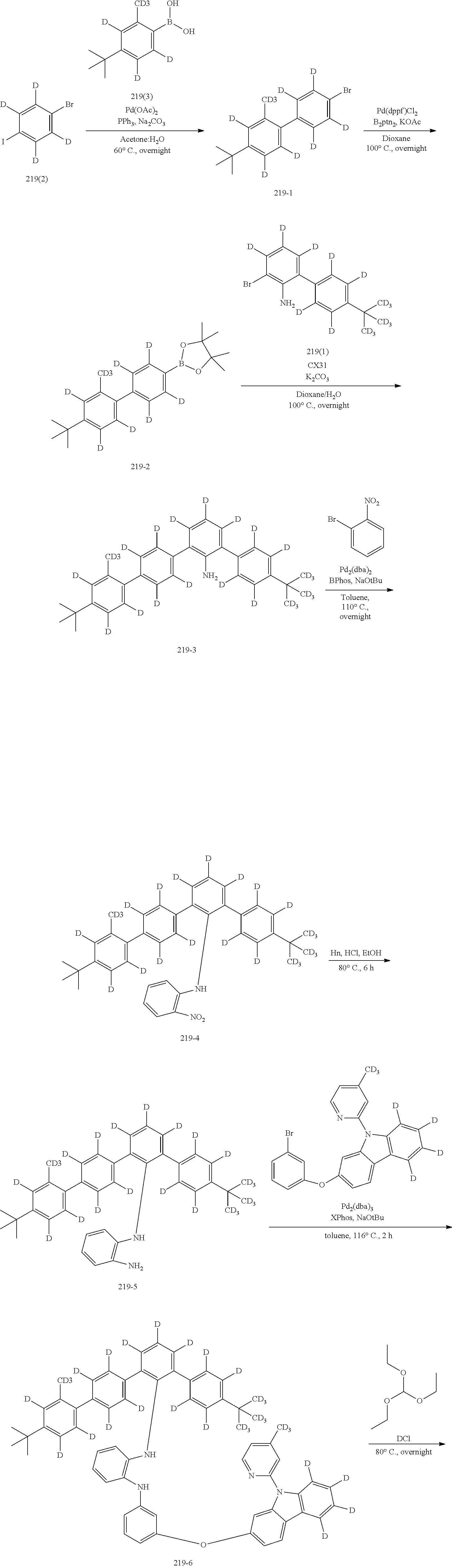

- Intermediate 219-1 was synthesized in substantially the same manner as utilized to synthesize Intermediate 197-1 of Synthesis Example 3, except that Compound 219(2) and Compound 219(3) were respectively utilized instead of 4-bromo-1-iodo-2-(methyl-d3)benzene and (2-(methyl-d3)phenyl)boronic acid.
- Intermediate 219-2 was synthesized in substantially the same manner as utilized to synthesize Intermediate 14-2 of Synthesis Example 1, except that Intermediate 219-1 was utilized instead of Intermediate 14-1.
- Intermediate 219-3 was synthesized in substantially the same manner as utilized to synthesize Intermediate 14-3 of Synthesis Example 1, except that Intermediate 219-2 and Compound 219(1) were utilized instead of Intermediate 14-2 and 3-bromo-3′,5′-di-tert-butyl-[1,1′-biphenyl]-2-amine.
- Intermediates 219-4 and 219-5 were sequentially synthesized in substantially the same manner as utilized to sequentially synthesize Intermediates 14-4 and 14-5 of Synthesis Example 1, except that Intermediates 219-3 and 219-4 were respectively utilized instead of Intermediates 14-3 and 14-4.
- Intermediate 219-6 was synthesized in substantially the same manner as utilized to synthesize Intermediate 14-6 of Synthesis Example 1, except that Intermediate 219-5 and 2-(3-bromophenoxy)-9-(4-(methyl-d3)pyridin-2-yl)-9H-carbazole-5,6,7,8-d4 were respectively utilized instead of Intermediate 14-5 and 2-(3-bromophenoxy)-9-(4-(2,2-dimethylpropyl-1,1-d2)pyridin-2-yl)-9H-carbazole.
- Intermediate 219-7 was synthesized in substantially the same manner as utilized to synthesize Intermediate 14-7 of Synthesis Example 1, except that Intermediate 219-6 was utilized instead of Intermediate 14-6. Synthesis of Compound 219
- Compound 219 (yield: 53%) was synthesized in substantially the same manner as utilized to synthesize Compound 14 of Synthesis Example 1, except that Intermediate 219-7 was utilized instead of Intermediate 14-7.
- ESI-LCMS for Compound 219: [M]+: C64H21D33N4OPt, 1123.5
-
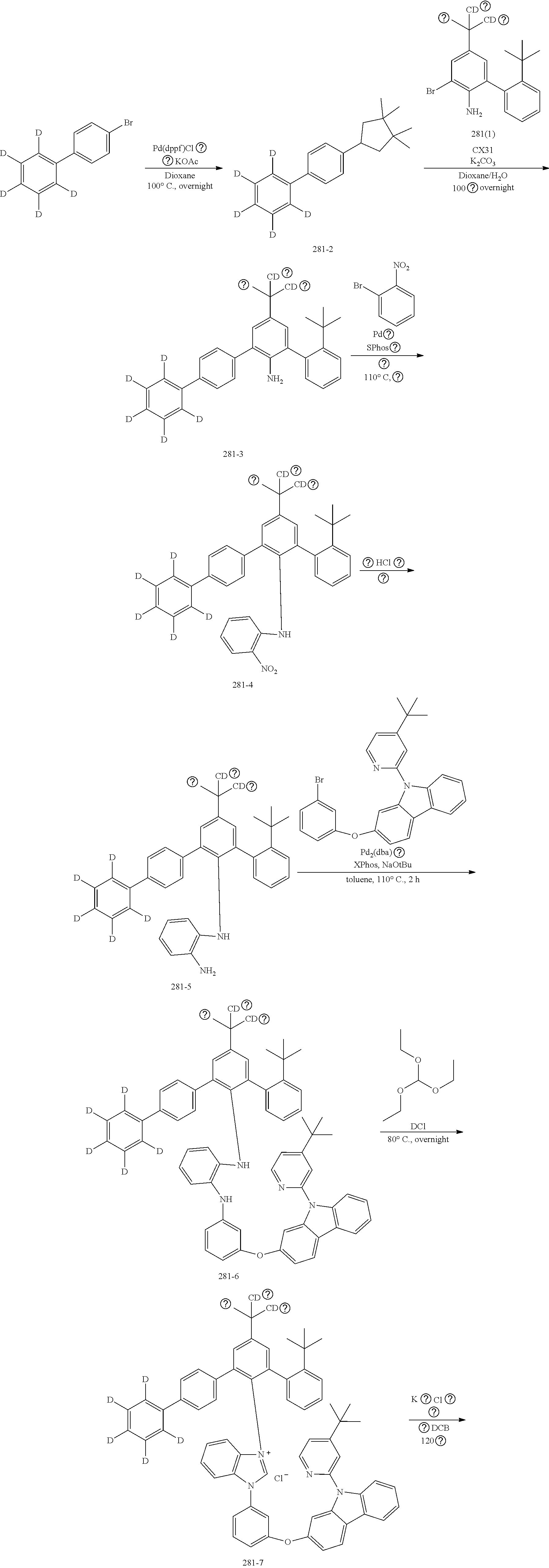
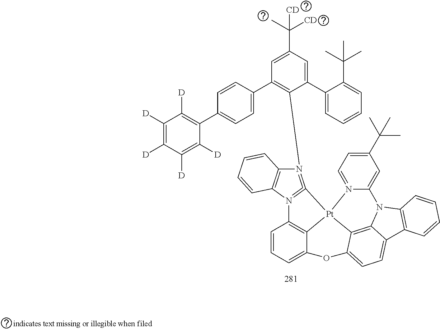
- Intermediate 281-2 was synthesized in substantially the same manner as utilized to synthesize Intermediate 14-2 of Synthesis Example 1, except that Compound 4-bromo-1,1′-biphenyl-2′,3′,4′,5′,6′-d5 was utilized instead of Intermediate 14-1.
- Intermediate 281-3 was synthesized in substantially the same manner as utilized to synthesize Intermediate 14-3 of Synthesis Example 1, except that Intermediate 281-2 and Compound 281(1) were utilized instead of Intermediate 14-2 and 3-bromo-3′,5′-di-tert-butyl-[1,1′-biphenyl]-2-amine.
- Intermediates 281-4 and 281-5 were sequentially synthesized in substantially the same manner as utilized to sequentially synthesize Intermediates 14-4 and 14-5 of Synthesis Example 1, except that Intermediates 281-3 and 281-4 were respectively utilized instead of Intermediates 14-3 and 14-4.
- Intermediate 281-6 was synthesized in substantially the same manner as utilized to synthesize Intermediate 14-6 of Synthesis Example 1, except that Intermediate 281-5 and 2-(3-bromophenoxy)-9-(4-(tert-butyl)pyridin-2-yl)-9H-carbazole were respectively utilized instead of Intermediate 14-5 and 2-(3-bromophenoxy)-9-(4-(2,2-dimethylpropyl-1,1-d2)pyridin-2-yl)-9H-carbazole.
- Intermediate 281-7 was synthesized in substantially the same manner as utilized to synthesize Intermediate 14-7 of Synthesis Example 1, except that Intermediate 281-6 was utilized instead of Intermediate 14-6.
- Compound 281 (yield: 56%) was synthesized in substantially the same manner as utilized to synthesize Compound 14 of Synthesis Example 1, except that Intermediate 281-7 was utilized instead of Intermediate 14-7.
- ESI-LCMS for Compound 281: [M]+: C66H44D14N4OPt, 1132.5
-

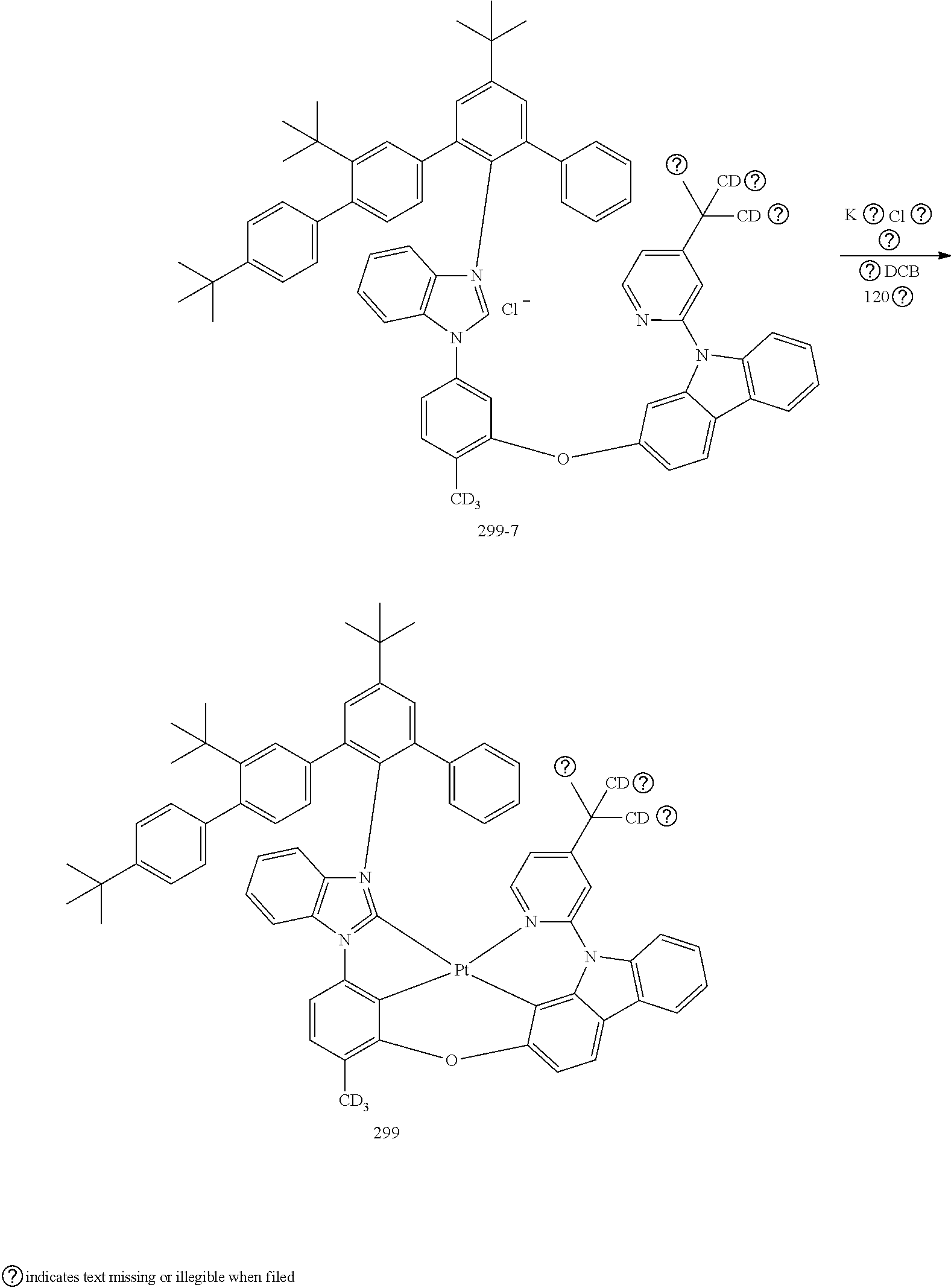
- Intermediate 299-2 was synthesized in substantially the same manner as utilized to synthesize Intermediate 14-2 of Synthesis Example 1, except that Compound 4-bromo-2,4′-di-tert-butyl-1,1′-biphenyl was utilized instead of Intermediate 14-1.
- Intermediate 299-3 was synthesized in substantially the same manner as utilized to synthesize Intermediate 14-3 of Synthesis Example 1, except that Intermediate 281-2 and Compound 299(1) were utilized instead of Intermediate 14-2 and 3-bromo-3′,5′-di-tert-butyl-[1,1′-biphenyl]-2-amine.
- Intermediates 299-4 and 299-5 were sequentially synthesized in substantially the same manner as utilized to sequentially synthesize Intermediates 14-4 and 14-5 of Synthesis Example 1, except that Intermediates 299-3 and 299-4 were respectively utilized instead of Intermediates 14-3 and 14-4.
- Intermediate 299-6 was synthesized in substantially the same manner as utilized to synthesize Intermediate 14-6 of Synthesis Example 1, except that Intermediate 299-5 and 2-(5-bromo-2-(methyl-d3)phenoxy)-9-(4-(2-(methyl-d3)propan-2-yl-1,1,1,3,3,3-d6)pyridin-2-yl)-9H-carbazole were respectively utilized instead of Intermediate 14-5 and 2-(3-bromophenoxy)-9-(4-(2,2-dimethylpropyl-1,1-d2)pyridin-2-yl)-9H-carbazole.
- Intermediate 299-7 was synthesized in substantially the same manner as utilized to synthesize Intermediate 14-7 of Synthesis Example 1, except that Intermediate 299-6 was utilized instead of Intermediate 14-6.
- Compound 299 (yield: 48%) was synthesized in substantially the same manner as utilized to synthesize Compound 14 of Synthesis Example 1, except that Intermediate 299-7 was utilized instead of Intermediate 14-7.
- ESI-LCMS for Compound 299: [M]+: C71H56D12N4OPt, 1200.6
-
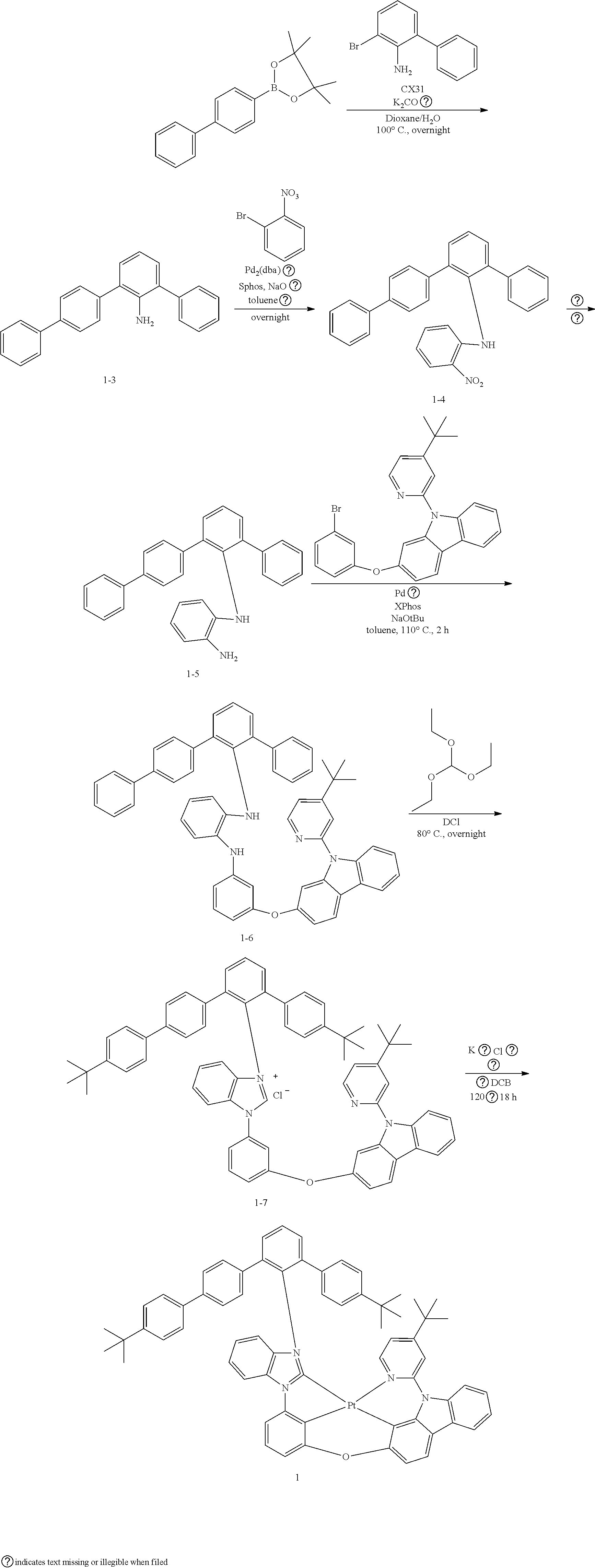
- Intermediate 1-3 was synthesized in substantially the same manner as utilized to synthesize Intermediate 14-3 of Synthesis Example 1, except that 2-([1,1′-biphenyl]-4-yl)-4,4,5,5-tetramethyl-1,3,2-dioxaborolane and 3-bromo-[1,1′-biphenyl]-2-amine were utilized instead of Intermediate 14-2 and 3-bromo-3′,5′-di-tert-butyl-[1,1′-biphenyl]-2-amine.
- Intermediates 1-4 and 1-5 were sequentially synthesized in substantially the same manner as utilized to sequentially synthesize Intermediates 14-4 and 14-5 of Synthesis Example 1, except that Intermediates 1-3 and 1-4 were respectively utilized instead of Intermediates 14-3 and 14-4.
- Intermediate 1-6 was synthesized in substantially the same manner as utilized to synthesize Intermediate 14-6 of Synthesis Example 1, except that Intermediate 1-5 and 2-(3-bromophenoxy)-9-(4-(tert-butyl)pyridin-2-yl)-9H-carbazole were respectively utilized instead of Intermediate 14-5 and 2-(3-bromophenoxy)-9-(4-(2,2-dimethylpropyl-1,1-d2)pyridin-2-yl)-9H-carbazole.
- Intermediate 1-7 was synthesized in substantially the same manner as utilized to synthesize Intermediate 14-7 of Synthesis Example 1, except that Intermediate 1-6 was utilized instead of Intermediate 14-6.
- Compound 1 (yield: 59%) was synthesized in substantially the same manner as utilized to synthesize Compound 14 of Synthesis Example 1, except that Intermediate 1-7 was utilized instead of Intermediate 14-7.
- ESI-LCMS for Compound 1: [M]+: C58H42N4OPt, 1006.1
-
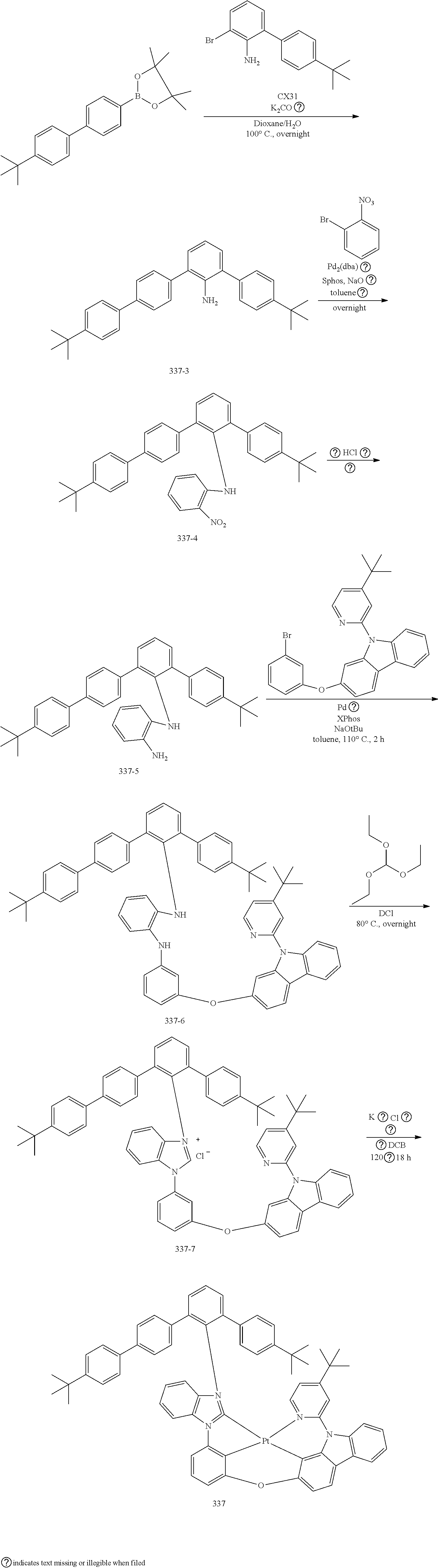
- Intermediate 337-3 was synthesized in substantially the same manner as utilized to synthesize Intermediate 14-3 of Synthesis Example 1, except that 2-(4′-(tert-butyl)-[1,1′-biphenyl]-4-yl)-4,4,5,5-tetramethyl-1,3,2-dioxaborolane and 3-bromo-4′-(tert-butyl)-[1,1′-biphenyl]-2-amine were utilized instead of Intermediate 14-2 and 3-bromo-3′,5′-di-tert-butyl-[1,1′-biphenyl]-2-amine.
- Intermediates 337-4 and 337-5 were sequentially synthesized in substantially the same manner as utilized to sequentially synthesize Intermediates 14-4 and 14-5 of Synthesis Example 1, except that Intermediates 337-3 and 337-4 were respectively utilized instead of Intermediates 14-3 and 14-4.
- Intermediate 337-6 was synthesized in substantially the same manner as utilized to synthesize Intermediate 14-6 of Synthesis Example 1, except that Intermediate 337-5 and 2-(3-bromophenoxy)-9-(4-(tert-butyl)pyridin-2-yl)-9H-carbazole were respectively utilized instead of Intermediate 14-5 and 2-(3-bromophenoxy)-9-(4-(2,2-dimethylpropyl-1,1-d2)pyridin-2-yl)-9H-carbazole.
- Intermediate 337-7 was synthesized in substantially the same manner as utilized to synthesize Intermediate 14-7 of Synthesis Example 1, except that Intermediate 337-6 was utilized instead of Intermediate 14-6.
- Compound 337 (yield: 48%) was synthesized in substantially the same manner as utilized to synthesize Compound 14 of Synthesis Example 1, except that Intermediate 337-7 was utilized instead of Intermediate 14-7.
- ESI-LCMS for Compound 337: [M]+: C66H58N4OPt, 1118.4
- For the compounds synthesized in Synthesis Examples 1 to 8, high-resolution mass (HR-MS) was measured, and results thereof are shown in Table 1. Synthesis methods of other compounds in addition to the compounds synthesized in Synthesis Examples 1 to 8 may be easily recognized by those of ordinary skill in the art by referring to the synthesis paths and source materials.
-
TABLE 1 HR-MS (m/z) [M+] Compound found calc. 14 1138.4 1138.38 54 1178.5 1178.43 197 1100.4 1100.31 219 1123.5 1123.45 281 1132.5 1132.39 299 1200.6 1200.51 1 1006.1 1006.09 337 1118.4 1118.30 - According to the methods of Table 2, the HOMO and LUMO energy levels of each of Compounds 14, 54, 197, 219, 281, 299, 1, 337, A, B, and C were evaluated, and results thereof are shown in Table 3.
-
TABLE 2 HOMO energy By utilizing cyclic voltammetry (CV) level evaluation (electrolyte: 0.1M Bu4NPF6/solvent: method dimethylformamide (DMF)/electrode: 3-electrode system (working electrode: GC, reference electrode: Ag/AgCl, and auxiliary electrode: Pt)), the potential (V)-current (A) graph of each compound was obtained, and then, from the oxidation onset of the graph, the HOMO energy level of each compound was calculated. LUMO energy By utilizing cyclic voltammetry (CV) level evaluation (electrolyte: 0.1M Bu4NPF6/solvent: method dimethylformamide (DMF)/electrode: 3-electrode system (working electrode: GC, reference electrode: Ag/AgCl, and auxiliary electrode: Pt)), the potential (V)-current (A) graph of each compound was obtained, and then, from the reduction onset of the graph, the LUMO energy level of each compound was calculated. -
TABLE 3 Compound No. HOMO (eV) LUMO (eV) 14 −5.30 −2.05 54 −5.29 −2.09 197 −5.32 −2.12 219 −5.30 −2.08 281 −5.26 −2.06 299 −5.28 −2.08 1 −5.28 −2.08 337 −5.26 −2.06 A −5.30 −2.18 B −5.32 −2.23 C −5.26 −1.89 


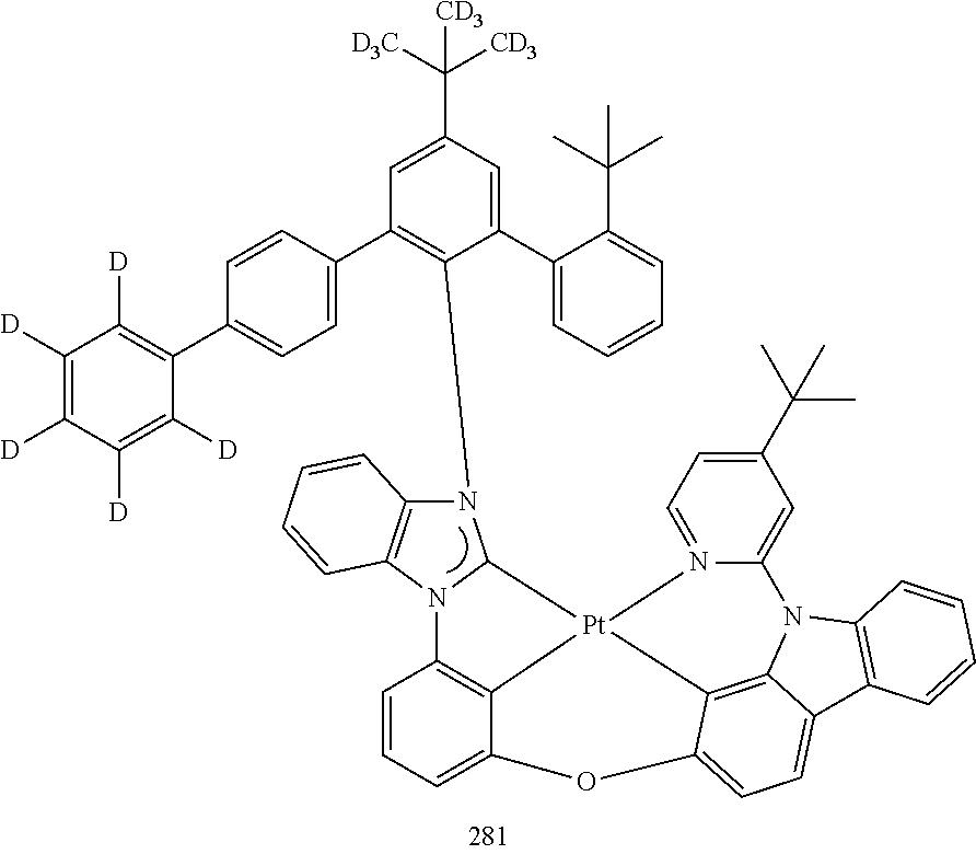
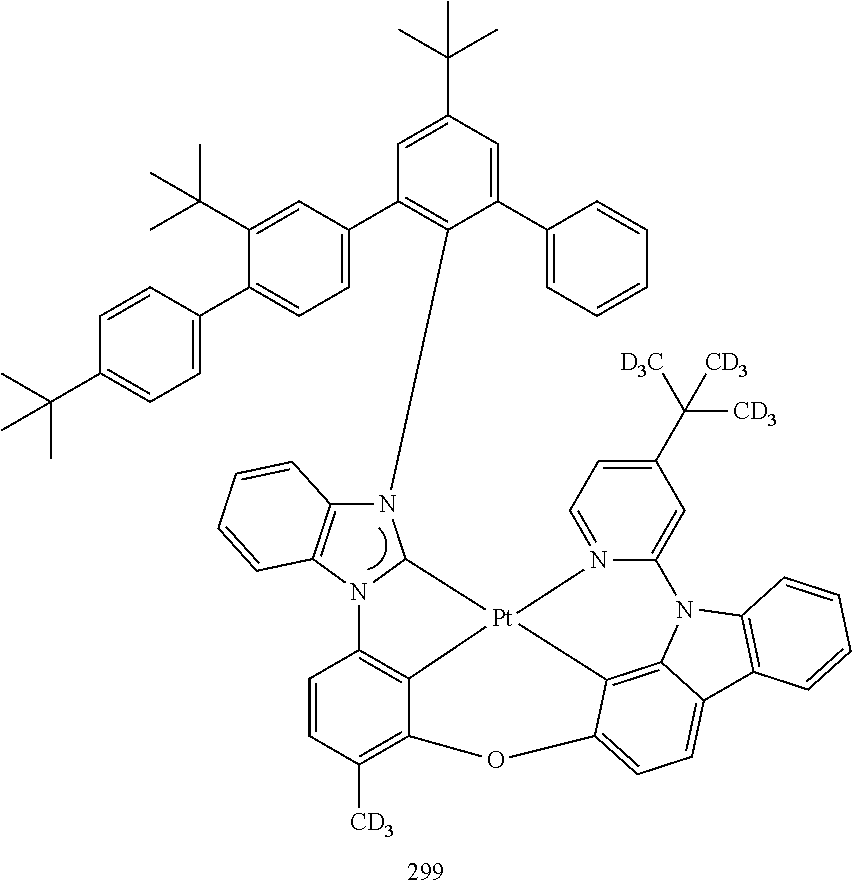


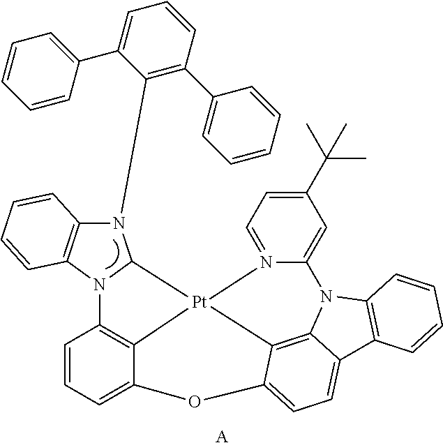


- After Compound 14 (2 mg), Compound ETH2 (10 mg), Compound HTH2 (10 mg), and PMMA in CH2Cl2 (the weight of PMMA is 50 mg) were mixed, a result obtained therefrom was coated on a quartz substrate by utilizing a spin coater, heat treated in an oven at 80° C., and then cooled to room temperature, to prepare Film 14 having a thickness of 40 nanometer (nm). Next, Films 54, 197, 219, 281, 299, 1, 337, A, B, and C were prepared in substantially the same manner as utilized to prepare Film 14, except that Compounds 54, 197, 219, 281, 299, 1, 337, A, B, and C were each utilized instead of Compound 14.
- The photoluminescence (PL) spectrum of each of Films 14, 54, 197, 219, 281, 299, 1, 337, A, B, and C was measured by a Quantaurus-QY Absolute PL quantum yield spectrometer (equipped with a xenon light source, a monochromator, a photonic multichannel analyzer, and an integrating sphere, and utilizing a photoluminescence quantum yield (PLQY) measurement software (Hamamatsu Photonics, Ltd., Shizuoka, Japan)) of Hamamatsu Company. During the measurement, the excitation wavelength was scanned from 320 nm to 380 nm at intervals of 10 nm, and the spectrum measured at the excitation wavelength of 340 nm was taken to obtain the maximum emission wavelength (emission peak wavelength) and full width at half maximum (FWHM) of the organometallic compound included in each Film, which are shown in Table 4.
- Next, the PLOY of each of Films 14, 54, 197, 219, 281, 299, 1, 337, A, B, and C was measured by scanning the excitation wavelength from 300 nm to 380 nm at intervals of 10 nm by utilizing a Quantaurus-QY Absolute PL quantum yield spectrometer of Hamamatsu Company, and then, the PLOY measured at the excitation wavelength of 330 nm was taken to obtain the PLOY of the organometallic compound included in each Film. Results thereof are shown in Table 4.
-
TABLE 4 Organometallic Maximum Emission Film compound No. emission FWHM PLQY No. included in Film wavelength (nm) (nm) (%) 14 14 457 37 60 54 54 457 38 57 197 197 456 35 63 219 219 457 38 58 281 281 455 37 65 299 299 455 36 61 1 1 457 37 56 337 337 455 35 59 A A 456 40 53 B B 458 41 47 C C 455 39 55 - From Table 4, it may be confirmed that each of Compounds 14, 54, 197, 219, 281, 299, 1, and 337 had improved PLOY and emitted blue light having a relatively small FWHM, as compared to Compounds A to C.
- Subsequently, the PL spectrum of each of Films 14, 54, 197, 219, 281, 299, 1, 337, A, B, and C was evaluated at room temperature by utilizing
FluoTime 300, which is a time-resolved photoluminescence (TRPL) measurement system of PicoQuant Inc., and PLS340 (excitation wavelength=340 nm, spectral width=20 nm), which is a pumping source of PicoQuant Inc., and then, the wavelength of the main peak of the spectrum was determined. The PLS340 repeated the measure of the number of photons emitted from each Film at the wavelength of the main peak by photon pulse (pulse width=500 picoseconds) applied to each Film, based on time-correlated single photon counting (TCSPC) according to time, to obtain a TRPL curve sufficient for fitting. A result thus obtained therefrom was fitted with one or more exponential decay functions to obtain Tdecay (Ex), that is, a decay time, of each of Films 14, 54, 197, 219, 281, 299, 1, 337, A, B, and C. Results thereof are shown in Table 5. A function for fitting is as shown in Equation 1, and from among Tdecay obtained from each exponential decay function utilized for fitting, the largest value was obtained as Tdecay(Ex). In this regard, the same measurement was performed during the same measurement time as that for obtaining TRPL curve in the dark state (in which pumping signals entering the set or predetermined film are blocked) to obtain a baseline or a background signal curve for utilization as a baseline for fitting. -
-
TABLE 5 Film Organometallic compound No. T No. included in Film (μs) 14 14 2.05 54 54 2.01 197 197 1.98 219 219 1.99 281 281 2.08 299 299 2.10 1 1 2.15 337 337 2.09 A A 2.25 B B 2.67 C C 2.45 - From Table 5, it may be confirmed that each of Compounds 14, 54, 197, 219, 281, 299, 1, and 337 had a relatively small emission decay time, as compared to Compounds A to C.
- As an anode, a glass substrate (product of Corning Inc.) with a 15 ohm per centimeter (Ω/cm2) (1,200 angstrom (A)) ITO formed thereon was cut to a size of 50 mm×50 mm×0.7 mm, sonicated by utilizing isopropyl alcohol and pure water each for 5 minutes, washed by irradiation of ultraviolet rays and exposure of ozone thereto for 30 minutes, and then mounted on a vacuum deposition apparatus.
- 2-TNATA was vacuum-deposited on the anode to form a hole injection layer having a thickness of 600 Å, and 4,4′-bis[N-(1-naphthyl)-N-phenylamino]biphenyl (hereinafter, referred as “NPB”) was vacuum-deposited on the hole injection layer to form a hole transport layer having a thickness of 300 Å.
- A first compound (Compound 14), a second compound (Compound ETH2), a third compound (Compound HTH29), and a fourth compound (Compound DFD051) were vacuum-deposited on the hole transport layer to form an emission layer having a thickness of 350 Å. In this regard, the amount of the first compound was 13 wt % based on the total amount (100 wt %) of the emission layer, the amount of the fourth compound was 1.3 wt % based on the total amount (100 wt %) of the emission layer, and the weight ratio of the second compound to the third compound was adjusted to 4:6.
- Compound ETH34 was vacuum-deposited on the emission layer to form a hole blocking layer having a thickness of 50 Å, and ET46 and LiQ were vacuum-deposited on the hole blocking layer at a weight ratio of 4:6 to form an electron transport layer having a thickness of 310 Å. Next, Yb was vacuum-deposited on the electron transport layer to form an electron injection layer having a thickness of 15 Å, and then Mg was vacuum-deposited thereon to form a cathode having a thickness of 800 Å, thereby completing manufacture of an organic light-emitting device.
-

- Organic light-emitting devices were manufactured in substantially the same manner as in Example 1, except that, in forming the emission layer, compounds shown in Table 6 were each utilized instead of Compound 14 as the first compound. The weight in parentheses in Table 6 indicates the weight of the corresponding compound based on 100 wt % of the emission layer.
- Each of the driving voltage (V) at 1,000 (candela per square meter (cd/m2)), color coordinate value (CIE(y)), y color conversion efficiency (candela per ampere per “y” (cd/A/y)), maximum emission wavelength (nanometer (nm)), and lifespan (T95) of the organic light-emitting devices manufactured in Examples 1 to 8 and Comparative Examples A to C were measured utilizing the Keithley MU 236 and the luminance meter PR650, and results thereof are shown in Table 7. In Table 7, the lifespan (T95) is a measure of the time (hour (h)) taken until the luminance reaches 95% of the initial luminance, and is expressed as a relative value (%).
-
TABLE 6 Weight ratio of second First Second Third Fourth compound to No. compound compound compound compound third compound Example 1 14 ETH2 HTH29 DFD051 4:6 (13 wt %) (1.3 wt %) Example 2 54 ETH2 HTH29 DFD051 4:6 (13 wt %) (1.3 wt %) Example 3 197 ETH2 HTH29 DFD051 4:6 (13 wt %) (1.3 wt %) Example 4 219 ETH2 HTH29 DFD051 4:6 (13 wt %) (1.3 wt %) Example 5 281 ETH2 HTH29 DFD051 4:6 (13 wt %) (1.3 wt %) Example 6 299 ETH2 HTH29 DFD051 4:6 (13 wt %) (1.3 wt %) Example 7 1 ETH2 HTH29 DFD051 4:6 (13 wt %) (1.3 wt %) Example 8 337 ETH2 HTH29 DFD051 4:6 (13 wt %) (1.3 wt %) Comparative A ETH2 HTH29 DFD051 4:6 Example A (13 wt %) (1.3 wt %) Comparative B ETH2 HTH29 DFD051 4:6 Example B (13 wt %) (1.3 wt %) Comparative C ETH2 HTH29 DFD051 4:6 Example C (13 wt %) (1.3 wt %) 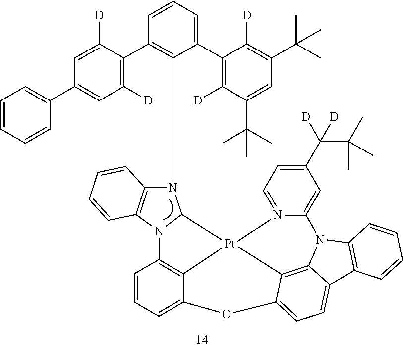
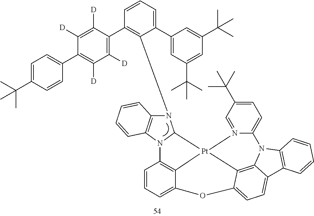

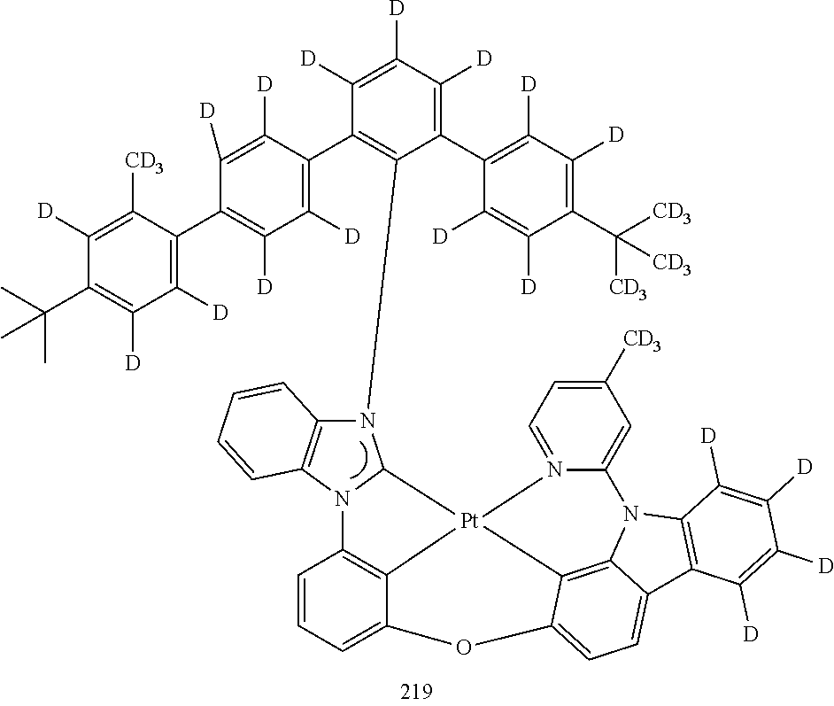
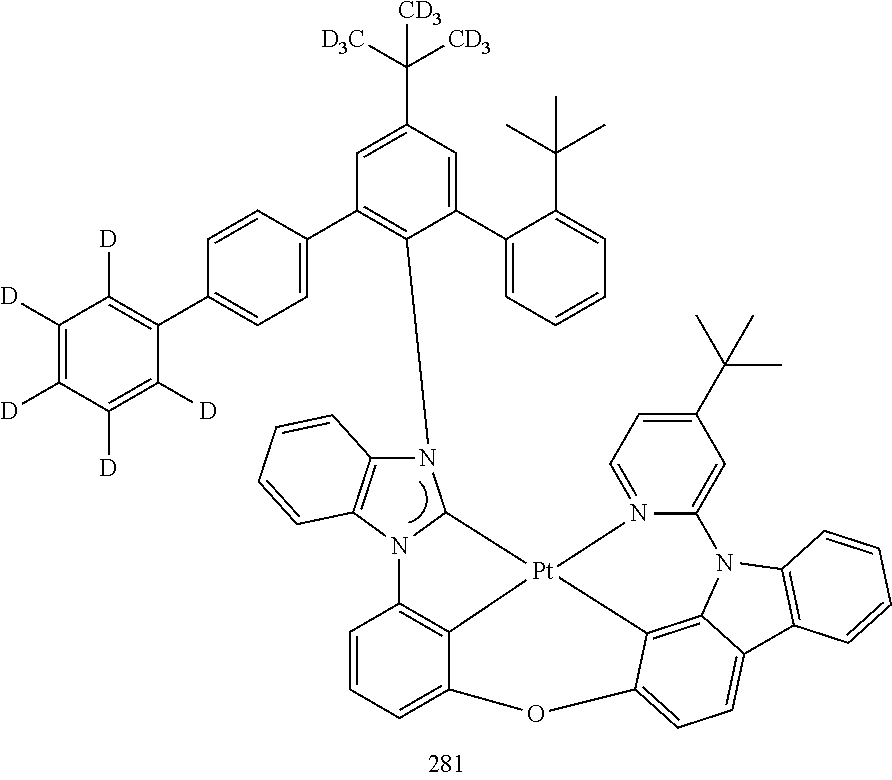


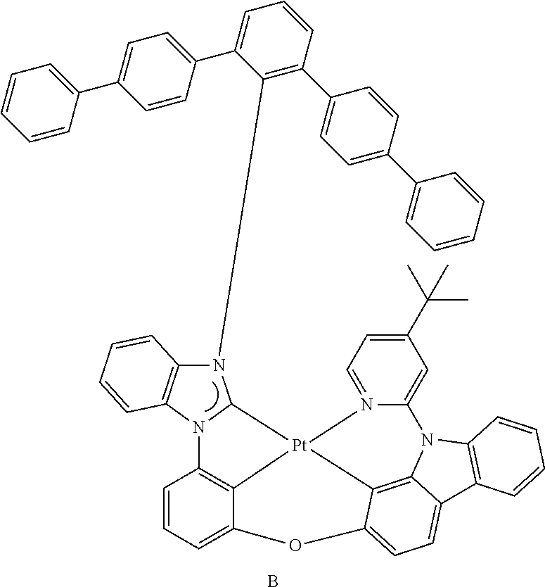
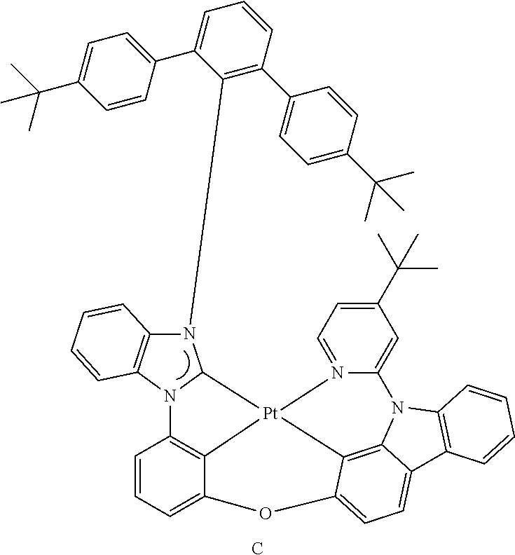

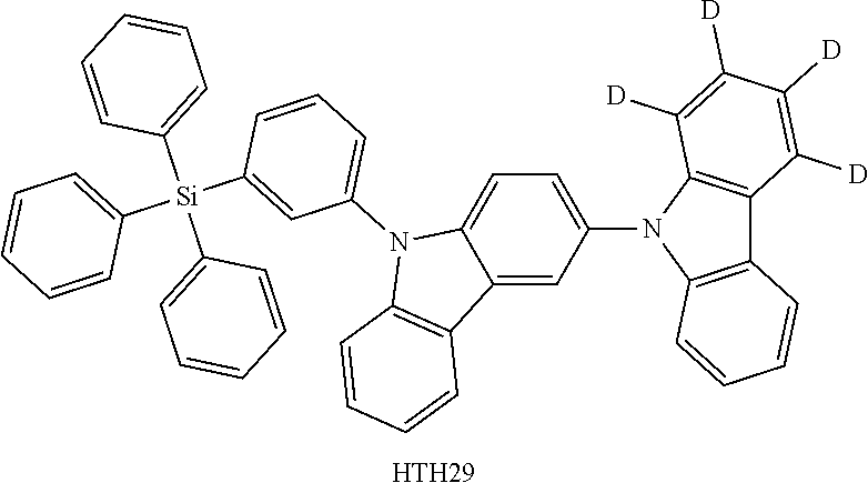

-
TABLE 7 Color Maximum Lifespan Driving conversion emission (T95) First Fourth Voltage Efficiency wavelength (Relative No. compound compound (V) CIE(y) (cd/A/y) (nm) value, %) Example 1 14 DFD051 4.14 0.109 152.4 462 168 Example 2 54 DFD051 4.11 0.104 145.6 461 160 Example 3 197 DFD051 4.19 0.106 155.7 461 179 Example 4 219 DFD051 4.21 0.105 148.9 461 184 Example 5 281 DFD051 4.25 0.112 159.3 462 158 Example 6 299 DFD051 4.23 0.114 155.4 462 151 Example 7 1 DFD051 4.26 0.120 137.2 463 145 Example 8 337 DFD051 4.24 0.118 142.5 462 149 Comparative A DFD051 4.32 0.117 129.8 462 125 Example A Comparative B DFD051 4.46 0.126 117.3 465 100 Example B Comparative C DFD051 4.37 0.121 132.4 463 117 Example C - From Table 7, it may be confirmed that the organic light-emitting devices of Examples 1 to 6 each emitted deep blue light and had excellent or suitable driving voltage, excellent or suitable color purity, excellent or suitable luminescence efficiency, excellent or suitable color conversion efficiency, and excellent or suitable lifespan characteristics. It may also be confirmed that the organic light-emitting devices of Examples 7 and 8 each emitted deep blue light and had improved characteristics in terms of driving voltage, color purity, color conversion efficiency, and lifespan, as compared to Comparative Examples A to C.
- Organic light-emitting devices were manufactured in substantially the same manner as in Example 1, except that, in forming the emission layer, compounds shown in Table 8 were each utilized as the first compound and the fourth compound, and the amounts of the first compound and the fourth compound and the weight ratio of the second compound to the third compound were each adjusted to those as shown in Table 8. The weight in parentheses in Table 8 indicates the weight of the corresponding compound based on 100 wt % of the emission layer.
- Each of the driving voltage (V) at 1,000 cd/m2, y color coordinate value (CIE(y)), color conversion efficiency (cd/A/y), maximum emission wavelength (nm), and lifespan (T95) of the organic light-emitting devices manufactured in Examples 11 to 18 and Comparative Examples 1A to 1C was measured in substantially the same manner as utilized in Evaluation Example 4, and results thereof are shown in Table 9. In Table 9, the lifespan (T95) is a measure of the time (h) taken until the luminance reaches 95% of the initial luminance, and is expressed as a relative value (%).
-
TABLE 8 Weight ratio of second First Second Third Fourth compound to No. compound compound compound compound third compound Example 14 ETH2 HTH29 DFD7 3:7 11 (14 wt %) (1.0 wt %) Example 54 ETH2 HTH29 DFD7 3:7 12 (14 wt %) (1.0 wt %) Example 197 ETH2 HTH29 DFD7 3:7 13 (14 wt %) (1.0 wt %) Example 219 ETH2 HTH29 DFD7 3:7 14 (14 wt %) (1.0 wt %) Example 281 ETH2 HTH29 DFD7 3:7 15 (14 wt %) (1.0 wt %) Example 299 ETH2 HTH29 DFD7 3:7 16 (14 wt %) (1.0 wt %) Example 1 ETH2 HTH29 DFD7 3:7 17 (14 wt %) (1.0 wt %) Example 337 ETH2 HTH29 DFD7 3:7 18 (14 wt %) (1.0 wt %) Comparative A ETH2 HTH29 DFD7 3:7 Example (14 wt %) (1.0 wt %) 1A Comparative B ETH2 HTH29 DFD7 3:7 Example (14 wt %) (1.0 wt %) 1B Comparative C ETH2 HTH29 DFD7 3:7 Example (14 wt %) (1.0 wt %) 1C 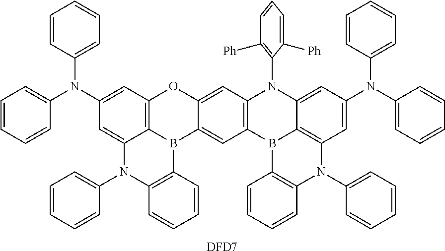
-
TABLE 9 Color Maximum Lifespan Driving conversion emission (T95) First Fourth Voltage Efficiency wavelength (Relative No. compound compound (V) CIE(y) (cd/A/y) (nm) value, %) Example 14 DFD07 4.36 0.133 129.8 463 179 11 Example 54 DFD07 4.42 0.128 123.4 462 182 12 Example 197 DFD07 4.51 0.124 122.3 462 167 13 Example 219 DFD07 4.53 0.136 121.7 463 202 14 Example 281 DFD07 4.47 0.139 136.6 464 173 15 Example 299 DFD07 4.43 0.121 130.2 464 171 16 Example 1 DFD07 4.49 0.138 117.8 464 149 17 Example 337 DFD07 4.45 0.132 119.5 463 158 18 Comparative A DFD07 4.61 0.137 115.7 465 137 Example 1A Comparative B DFD07 4.72 0.154 103.4 466 100 Example 1B Comparative C DFD07 4.68 0.145 118.3 465 122 Example 1C - From Table 9, it may be confirmed that the organic light-emitting devices of Examples 11 to 16 each emitted deep blue light and had excellent or suitable driving voltage, excellent or suitable color purity, excellent or suitable luminescence efficiency, excellent or suitable color conversion efficiency, and excellent or suitable lifespan characteristics. It may also be confirmed that the organic light-emitting devices of Examples 17 and 18 each emitted deep blue light and had improved characteristics in terms of driving voltage, color purity, color conversion efficiency, and lifespan, as compared to Comparative Examples 1A to 1C.
- The organometallic compound has excellent or suitable processability and excellent or suitable electrical characteristics, and thus a light-emitting device including the organometallic compound may have improved color purity, improved luminescence efficiency, and improved lifespan.
- It should be understood that embodiments described herein should be considered in a descriptive sense only and not for purposes of limitation. Descriptions of features or aspects within each embodiment should typically be considered as available for other similar features or aspects in other embodiments. While one or more embodiments have been described with reference to the drawings, it will be understood by those of ordinary skill in the art that one or more suitable changes in form and details may be made therein without departing from the spirit and scope as defined by the following claims and equivalents thereof.
Claims (20)
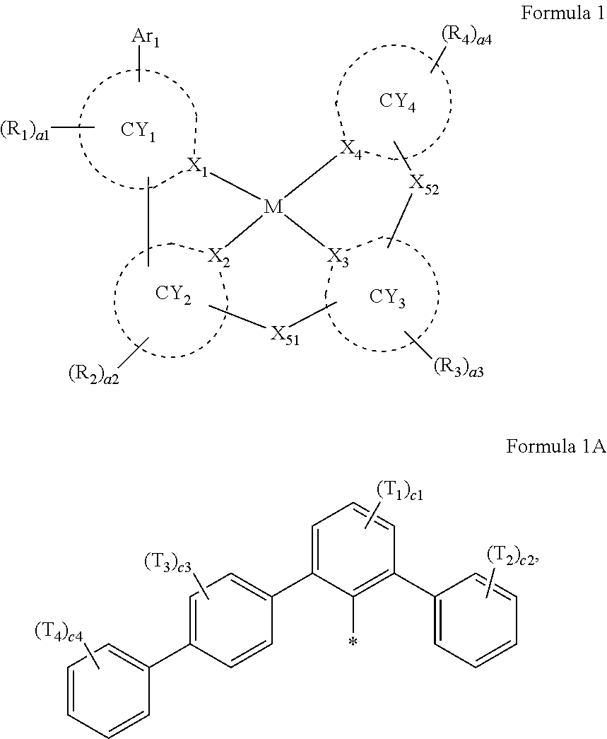


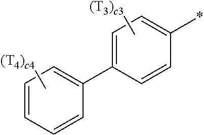

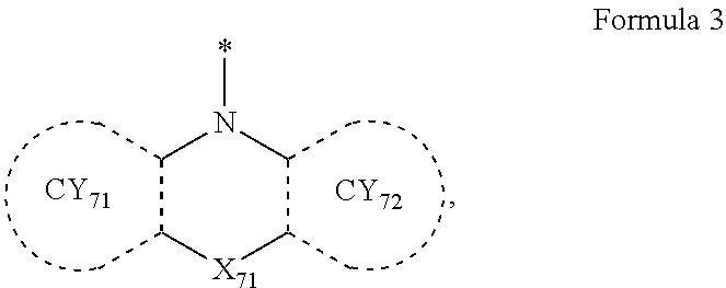
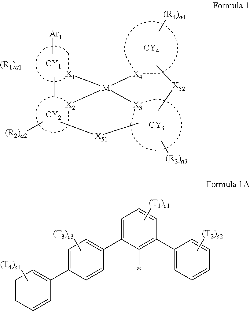


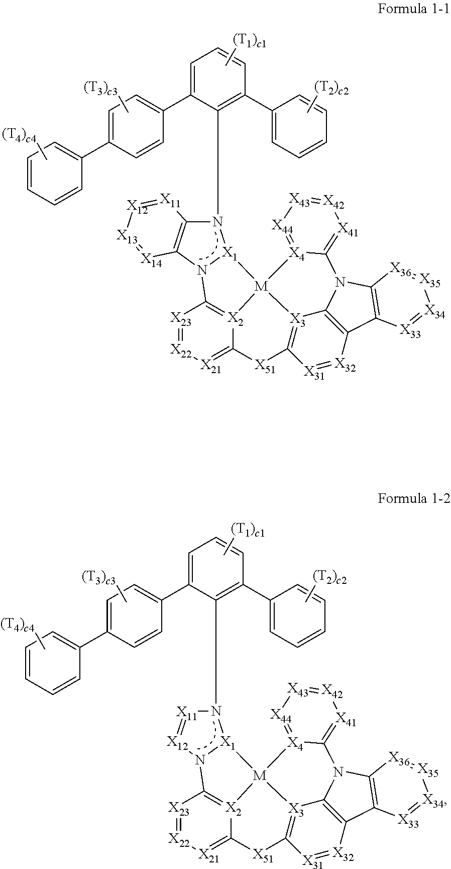

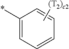
Applications Claiming Priority (2)
| Application Number | Priority Date | Filing Date | Title |
|---|---|---|---|
| KR10-2023-0121344 | 2023-09-12 | ||
| KR1020230121344A KR20250038889A (en) | 2023-09-12 | 2023-09-12 | Composition, light emitting device, electronic device including the same and organometallic compound |
Publications (1)
| Publication Number | Publication Date |
|---|---|
| US20250098518A1 true US20250098518A1 (en) | 2025-03-20 |
Family
ID=94905370
Family Applications (1)
| Application Number | Title | Priority Date | Filing Date |
|---|---|---|---|
| US18/830,437 Pending US20250098518A1 (en) | 2023-09-12 | 2024-09-10 | Composition, light-emitting device, electronic apparatus including the light-emitting device, and organometallic compound |
Country Status (3)
| Country | Link |
|---|---|
| US (1) | US20250098518A1 (en) |
| KR (1) | KR20250038889A (en) |
| CN (1) | CN119613458A (en) |
-
2023
- 2023-09-12 KR KR1020230121344A patent/KR20250038889A/en active Pending
-
2024
- 2024-09-10 US US18/830,437 patent/US20250098518A1/en active Pending
- 2024-09-10 CN CN202411261907.3A patent/CN119613458A/en active Pending
Also Published As
| Publication number | Publication date |
|---|---|
| KR20250038889A (en) | 2025-03-20 |
| CN119613458A (en) | 2025-03-14 |
Similar Documents
| Publication | Publication Date | Title |
|---|---|---|
| US12520717B2 (en) | Light-emitting device and electronic apparatus including same | |
| US20230172053A1 (en) | Composition, light-emitting device, electronic apparatus, consumer product, and organometallic compound | |
| US20240244870A1 (en) | Light-emitting device, electronic device including the same, and electronic apparatus including the same | |
| US20240023361A1 (en) | Light-emitting device, electronic device including the same, and electronic apparatus includuing the same | |
| US20250098517A1 (en) | Light-emitting device, electronic apparatus including the light-emitting device, and electronic equipment including the electronic apparatus | |
| US20230225145A1 (en) | Light-emitting device and electronic apparatus including the same | |
| US20230380262A1 (en) | Light-emitting device, electronic device including the same, and electronic apparatus including the same | |
| US20250098518A1 (en) | Composition, light-emitting device, electronic apparatus including the light-emitting device, and organometallic compound | |
| US20220289779A1 (en) | Organometallic compound and organic light-emitting device including the same | |
| US20250169354A1 (en) | Composition, light-emitting device, electronic equipment including the light-emitting device, and organometallic compound | |
| US20250115632A1 (en) | Composition, light-emitting device and electronic equipment including the same, and organometallic compound | |
| US20240051981A1 (en) | Composition, light-emitting device, electronic apparatus including the light-emitting device, and organometallic compound | |
| US20240268215A1 (en) | Light-emitting device including organometallic compound, electronic apparatus including the light-emitting device, and the organometallic compound | |
| US20240292742A1 (en) | Light-emitting device including heterocyclic compound, electronic apparatus including light-emitting device, and heterocyclic compound | |
| US20240284782A1 (en) | Light-emitting device including organometallic compound, electronic apparatus including the light-emitting device, the organometallic compound | |
| US20240268224A1 (en) | Light-emitting device including organometallic compound, electronic apparatus including the light-emitting device, and the organometallic compound | |
| US20240180022A1 (en) | Light-emitting device including organometallic compound, electronic device including the light-emitting device, and the organometallic compound | |
| US20240196637A1 (en) | Composition, light-emitting device, and electronic device including light-emitting device | |
| US20230422597A1 (en) | Light-emitting device, electronic apparatus including the light-emitting device, and electronic device including the light-emitting device | |
| US20240260290A1 (en) | Composition, light-emitting device, and electronic apparatus including the same | |
| US20230225185A1 (en) | Light-emitting device and electronic apparatus including the same | |
| US12389792B2 (en) | Light-emitting device and electronic apparatus including the same | |
| US20240164208A1 (en) | Organic compound and light-emitting device including the same | |
| US20240260449A1 (en) | Light-emitting device including organometallic compound, electronic apparatus including light-emitting device, and organometallic compound | |
| US20250133957A1 (en) | Compound, light-emitting device including the same, and electronic apparatus including the light-emitting device |
Legal Events
| Date | Code | Title | Description |
|---|---|---|---|
| AS | Assignment |
Owner name: SAMSUNG DISPLAY CO., LTD., KOREA, REPUBLIC OF Free format text: ASSIGNMENT OF ASSIGNORS INTEREST;ASSIGNORS:OH, CHANSEOK;KANG, ILJOON;KO, SOOBYUNG;AND OTHERS;REEL/FRAME:068646/0450 Effective date: 20240213 Owner name: SAMSUNG DISPLAY CO., LTD., KOREA, REPUBLIC OF Free format text: ASSIGNMENT OF ASSIGNOR'S INTEREST;ASSIGNORS:OH, CHANSEOK;KANG, ILJOON;KO, SOOBYUNG;AND OTHERS;REEL/FRAME:068646/0450 Effective date: 20240213 |
|
| STPP | Information on status: patent application and granting procedure in general |
Free format text: DOCKETED NEW CASE - READY FOR EXAMINATION |