US20240199816A1 - Photocurable composition with high silicon content - Google Patents
Photocurable composition with high silicon content Download PDFInfo
- Publication number
- US20240199816A1 US20240199816A1 US18/062,374 US202218062374A US2024199816A1 US 20240199816 A1 US20240199816 A1 US 20240199816A1 US 202218062374 A US202218062374 A US 202218062374A US 2024199816 A1 US2024199816 A1 US 2024199816A1
- Authority
- US
- United States
- Prior art keywords
- photocurable composition
- silicon
- alkylaryl
- aryl
- alkyl
- Prior art date
- Legal status (The legal status is an assumption and is not a legal conclusion. Google has not performed a legal analysis and makes no representation as to the accuracy of the status listed.)
- Pending
Links
Classifications
-
- C—CHEMISTRY; METALLURGY
- C08—ORGANIC MACROMOLECULAR COMPOUNDS; THEIR PREPARATION OR CHEMICAL WORKING-UP; COMPOSITIONS BASED THEREON
- C08G—MACROMOLECULAR COMPOUNDS OBTAINED OTHERWISE THAN BY REACTIONS ONLY INVOLVING UNSATURATED CARBON-TO-CARBON BONDS
- C08G77/00—Macromolecular compounds obtained by reactions forming a linkage containing silicon with or without sulfur, nitrogen, oxygen or carbon in the main chain of the macromolecule
- C08G77/04—Polysiloxanes
- C08G77/22—Polysiloxanes containing silicon bound to organic groups containing atoms other than carbon, hydrogen and oxygen
-
- C—CHEMISTRY; METALLURGY
- C09—DYES; PAINTS; POLISHES; NATURAL RESINS; ADHESIVES; COMPOSITIONS NOT OTHERWISE PROVIDED FOR; APPLICATIONS OF MATERIALS NOT OTHERWISE PROVIDED FOR
- C09D—COATING COMPOSITIONS, e.g. PAINTS, VARNISHES OR LACQUERS; FILLING PASTES; CHEMICAL PAINT OR INK REMOVERS; INKS; CORRECTING FLUIDS; WOODSTAINS; PASTES OR SOLIDS FOR COLOURING OR PRINTING; USE OF MATERIALS THEREFOR
- C09D183/00—Coating compositions based on macromolecular compounds obtained by reactions forming in the main chain of the macromolecule a linkage containing silicon, with or without sulfur, nitrogen, oxygen, or carbon only; Coating compositions based on derivatives of such polymers
- C09D183/04—Polysiloxanes
-
- C—CHEMISTRY; METALLURGY
- C08—ORGANIC MACROMOLECULAR COMPOUNDS; THEIR PREPARATION OR CHEMICAL WORKING-UP; COMPOSITIONS BASED THEREON
- C08F—MACROMOLECULAR COMPOUNDS OBTAINED BY REACTIONS ONLY INVOLVING CARBON-TO-CARBON UNSATURATED BONDS
- C08F230/00—Copolymers of compounds having one or more unsaturated aliphatic radicals, each having only one carbon-to-carbon double bond, and containing phosphorus, selenium, tellurium or a metal
- C08F230/04—Copolymers of compounds having one or more unsaturated aliphatic radicals, each having only one carbon-to-carbon double bond, and containing phosphorus, selenium, tellurium or a metal containing a metal
- C08F230/08—Copolymers of compounds having one or more unsaturated aliphatic radicals, each having only one carbon-to-carbon double bond, and containing phosphorus, selenium, tellurium or a metal containing a metal containing silicon
- C08F230/085—Copolymers of compounds having one or more unsaturated aliphatic radicals, each having only one carbon-to-carbon double bond, and containing phosphorus, selenium, tellurium or a metal containing a metal containing silicon the monomer being a polymerisable silane, e.g. (meth)acryloyloxy trialkoxy silanes or vinyl trialkoxysilanes
-
- C—CHEMISTRY; METALLURGY
- C08—ORGANIC MACROMOLECULAR COMPOUNDS; THEIR PREPARATION OR CHEMICAL WORKING-UP; COMPOSITIONS BASED THEREON
- C08G—MACROMOLECULAR COMPOUNDS OBTAINED OTHERWISE THAN BY REACTIONS ONLY INVOLVING UNSATURATED CARBON-TO-CARBON BONDS
- C08G77/00—Macromolecular compounds obtained by reactions forming a linkage containing silicon with or without sulfur, nitrogen, oxygen or carbon in the main chain of the macromolecule
- C08G77/04—Polysiloxanes
- C08G77/14—Polysiloxanes containing silicon bound to oxygen-containing groups
- C08G77/18—Polysiloxanes containing silicon bound to oxygen-containing groups to alkoxy or aryloxy groups
-
- C—CHEMISTRY; METALLURGY
- C08—ORGANIC MACROMOLECULAR COMPOUNDS; THEIR PREPARATION OR CHEMICAL WORKING-UP; COMPOSITIONS BASED THEREON
- C08G—MACROMOLECULAR COMPOUNDS OBTAINED OTHERWISE THAN BY REACTIONS ONLY INVOLVING UNSATURATED CARBON-TO-CARBON BONDS
- C08G77/00—Macromolecular compounds obtained by reactions forming a linkage containing silicon with or without sulfur, nitrogen, oxygen or carbon in the main chain of the macromolecule
- C08G77/04—Polysiloxanes
- C08G77/20—Polysiloxanes containing silicon bound to unsaturated aliphatic groups
-
- C—CHEMISTRY; METALLURGY
- C09—DYES; PAINTS; POLISHES; NATURAL RESINS; ADHESIVES; COMPOSITIONS NOT OTHERWISE PROVIDED FOR; APPLICATIONS OF MATERIALS NOT OTHERWISE PROVIDED FOR
- C09D—COATING COMPOSITIONS, e.g. PAINTS, VARNISHES OR LACQUERS; FILLING PASTES; CHEMICAL PAINT OR INK REMOVERS; INKS; CORRECTING FLUIDS; WOODSTAINS; PASTES OR SOLIDS FOR COLOURING OR PRINTING; USE OF MATERIALS THEREFOR
- C09D183/00—Coating compositions based on macromolecular compounds obtained by reactions forming in the main chain of the macromolecule a linkage containing silicon, with or without sulfur, nitrogen, oxygen, or carbon only; Coating compositions based on derivatives of such polymers
- C09D183/04—Polysiloxanes
- C09D183/08—Polysiloxanes containing silicon bound to organic groups containing atoms other than carbon, hydrogen, and oxygen
-
- C—CHEMISTRY; METALLURGY
- C09—DYES; PAINTS; POLISHES; NATURAL RESINS; ADHESIVES; COMPOSITIONS NOT OTHERWISE PROVIDED FOR; APPLICATIONS OF MATERIALS NOT OTHERWISE PROVIDED FOR
- C09D—COATING COMPOSITIONS, e.g. PAINTS, VARNISHES OR LACQUERS; FILLING PASTES; CHEMICAL PAINT OR INK REMOVERS; INKS; CORRECTING FLUIDS; WOODSTAINS; PASTES OR SOLIDS FOR COLOURING OR PRINTING; USE OF MATERIALS THEREFOR
- C09D4/00—Coating compositions, e.g. paints, varnishes or lacquers, based on organic non-macromolecular compounds having at least one polymerisable carbon-to-carbon unsaturated bond ; Coating compositions, based on monomers of macromolecular compounds of groups C09D183/00 - C09D183/16
-
- C—CHEMISTRY; METALLURGY
- C08—ORGANIC MACROMOLECULAR COMPOUNDS; THEIR PREPARATION OR CHEMICAL WORKING-UP; COMPOSITIONS BASED THEREON
- C08G—MACROMOLECULAR COMPOUNDS OBTAINED OTHERWISE THAN BY REACTIONS ONLY INVOLVING UNSATURATED CARBON-TO-CARBON BONDS
- C08G77/00—Macromolecular compounds obtained by reactions forming a linkage containing silicon with or without sulfur, nitrogen, oxygen or carbon in the main chain of the macromolecule
- C08G77/04—Polysiloxanes
- C08G77/045—Polysiloxanes containing less than 25 silicon atoms
Definitions
- the present disclosure relates to a photocurable composition, particularly to a photo-curable composition for inkjet adaptive planarization adapted for forming photo-cured layers having a high silicon content.
- IAP Inkjet Adaptive Planarization
- a substrate e.g., a wafer containing an electric circuit
- jetting liquid drops of a photocurable composition on the surface of the substrate and bringing a flat superstrate in direct contact with the added liquid to form a flat liquid layer.
- the flat liquid layer is typically solidified under UV light exposure, and after removal of the superstrate a planar polymeric surface is obtained, which can be subjected to subsequent processing steps, for example baking, etching, and/or further deposition steps.
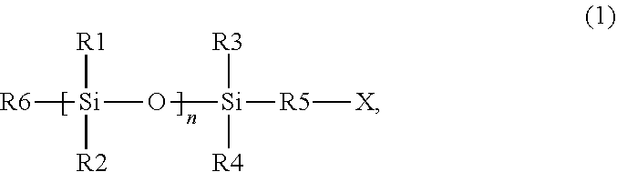
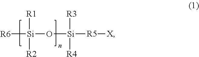
- a photocurable composition can comprise a photocurable composition comprising a polymerizable material and a photoinitiator, wherein the polymerizable material can include at least one silicon-containing monomer having a structure of formula (1)
- the amount of Si can be at least 20 wt % based on the total weight of the photocurable composition.
- the molecular weight of the silicon-containing monomer can be at least 100 g/mol and not greater than 800 g/mol.
- the amount of the at least one silicon-containing monomer can be at least 60 wt % based on the total weight of the polymerizable material. In a particular aspect, the amount of the at least one silicon-containing monomer can be at least 60 wt % and not greater than 85 wt % based on the total weight of the polymerizable material.
- the viscosity of the photocurable composition can be not greater than 20 mPa ⁇ s.
- the amount of the polymerizable material can be at least 90 wt % based on the total weight of the photocurable composition.
- the photocurable composition can be essentially free of a solvent.
- the at least one silicon-containing monomer can include at least two different silicon-containing monomers.
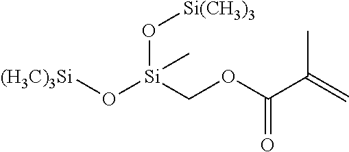
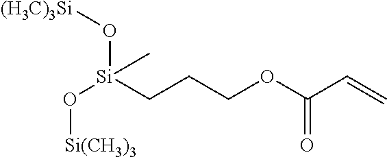
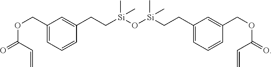
- the at least one silicon-containing monomer can be selected from the group of methacryloxymethyltris(trimethylsiloxane)silane (SiM1), 1,3-bis(3-methacryloxypropyl)tetrakis(trimethylsiloxy)disiloxane (SiM2), 3-acryloxypropyltris(trimethylsiloxy)silane (SiM3), (methacryloxymethyl)bis(trimethylsiloxy)methylsilane (SiM4), 3-methacryloxypropylbis(trimethylsiloxy)methylsilane (SiM5), (3-acryloxypropyl)methylbis(trimethylsiloxy)silane (SiM6), methacryloxypropyltris(trimethylsiloxy)silane (SiM7), acryloxymethyltrimethylsilane (SiM8), acryloxymethyltris(trimethylsiloxy)silane (SiM9), 1,3-bis[(acryloxymethylmethyltri
- the at least one silicon-containing monomer can include methacryloxymethyltris(trimethylsiloxane)silane (SiM1), or 1,3-bis(3-methacryloxypropyl)tetrakis(trimethylsiloxy)disiloxane (SiM2), or 3-acryloxypropyl-tris(trimethylsiloxy)silane (SiM3), or any combination thereof.
- SiM1 methacryloxymethyltris(trimethylsiloxane)silane
- SiM2 1,3-bis(3-methacryloxypropyl)tetrakis(trimethylsiloxy)disiloxane
- SiM3 3-acryloxypropyl-tris(trimethylsiloxy)silane
- the photocurable composition can comprise at least one polymerizable monomer not containing silicon.
- the polymerizable monomer not containing silicon can include an acrylate monomer.
- the acrylate monomer can include benzyl acrylate (BA); isobornyl acrylate (IBOA); 1,5-pentanediol diacrylate (MPDA); dihydrodicyclopentadienyl acrylate (DCPA); tricyclodecane dimethanol diacrylate (A-DCP); 2-Propenoic acid, 1-phenyl-1,2-ethanediyl ester (PHEDA); or any combination thereof.
- BA benzyl acrylate
- IBOA isobornyl acrylate
- MPDA 1,5-pentanediol diacrylate
- DCPA dihydrodicyclopentadienyl acrylate
- A-DCP 2-Propenoic acid, 1-phenyl-1,2-ethanediyl ester
- a laminate in another embodiment, can comprise a substrate and a photo-cured layer overlying the substrate, wherein the photo-cured layer is formed from the above-described photocurable composition.
- a method of forming a photo-cured layer on a substrate can comprise: applying a layer of a photocurable composition on the substrate, wherein the photocurable composition comprises a polymerizable material and at least one photoinitiator, and wherein the polymerizable material comprises at least one silicon-containing monomer having a structure of formula (1)
- the amount of Si can be at least 20 wt % based on the total weight of the photocurable composition.
- the viscosity of the photocurable composition may be not greater than 20 mPa ⁇ s.
- the amount of the polymerizable material can be at least 90 wt % based on the total weight of the photocurable composition.
- a method of manufacturing an article can comprise: applying a layer of a photocurable composition on a substrate, wherein the photocurable composition comprises a polymerizable material and at least one photoinitiator, wherein the polymerizable material comprises at least one silicon-containing monomer having a structure of formula (1)
- n: 0-4; and an amount of silicon (Si) in the photocurable composition may be at least 15 wt % based on the total weight of the photocurable; bringing the photocurable composition into contact with a template or a superstrate; irradiating the photocurable composition with light to form a photo-cured layer; removing the template or the superstrate from the photo-cured layer;
- the terms “comprises,” “comprising,” “includes,” “including,” “has,” “having” or any other variation thereof, are intended to cover a non-exclusive inclusion.
- a process, method, article, or apparatus that comprises a list of features is not necessarily limited only to those features but may include other features not expressly listed or inherent to such process, method, article, or apparatus.
- the present disclosure is directed to a photocurable composition
- a photocurable composition comprising a polymerizable material and a photoinitiator, wherein the polymerizable material comprises at least one silicon-containing monomer having a structure of formula (1)
- the amount of silicon (Si) in the photocurable composition can be at least 15 wt % based on the total weight of the photocurable composition.
- silicon-containing monomer refers to a monomer falling under the structure of formula (1).
- the amount of silicon in the photocurable composition can be at least 16 wt % based on the total weight of the photocurable composition, such as at least 17 wt %, at least 18 wt %, at least 19 wt %, or at least 20 wt %. In other aspects, the amount of silicon in the photocurable composition may be not greater than 33 wt %, or not greater than 30 wt %, or not greater than 28 wt %, or not greater than 25 wt %.
- the molecular weight of the silicon-containing monomer can be at least 100 g/mol, or at least 200 g/mol, or at least 300 g/mol, or at least 400 g/mol. In other aspects, the molecular weight of the silicon-containing monomer may be not greater than 800 g/mol, or not be greater than 700 g/mol, or not greater than 600 g/mol, or not greater than 500 g/mol, or not greater than 400 g/mol.
- the amount of the at least one silicon-containing monomer can be at least 60 wt % based on the total weight of the polymerizable material, such as at least 65 wt %, or at least 70 wt %, or at least 80 wt %, or at least 90 wt %, or at least 95 wt %, or 100 wt %.
- the amount of the silicon-containing monomer may be not greater than 99 wt % based on the total weight of the polymerizable material, or not greater than 95 wt %, or not greater than 90 wt %, or not greater than 85 wt %.
- the amount of the silicon-containing monomer can be at least 60 wt % and not greater than 85 wt % based on the total weight of the polymerizable material.
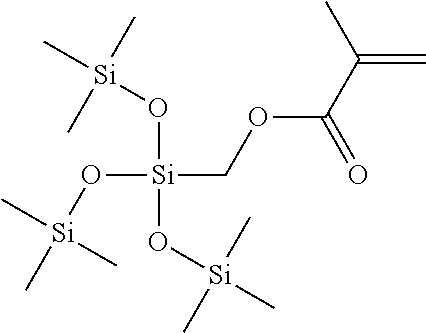
- Non-limiting example structure of polymerizable monomers falling under the structure of formula (1) of the silicon-containing monomer can be: methacryloxymethyltris(trimethylsiloxane)silane (SiM1):
- SiM7 methacryloxypropyltris(trimethylsiloxy)silane
- the photocurable composition of the present disclosure can be designed of having a low viscosity before curing.
- the viscosity of the curable composition can be not greater than 30 mPa ⁇ s, or not greater than 25 mPa ⁇ s, or not greater than 20 mPa ⁇ s, or not greater than 15 mPa ⁇ s, or not greater than 10 mPa ⁇ s.
- the viscosity may be at least 5 mPa ⁇ s.
- the photocurable composition can have a viscosity from 5 mPa ⁇ s to not greater than 20 mPa ⁇ s.
- all viscosity values relate to viscosities measured at a temperature of 23° C. with the Brookfield method using a Brookfield Viscometer.
- the polymerizable material of photocurable composition can further include at least one polymerizable monomer not containing silicon, such as one or more mono-functional and/or one or more multi-functional polymerizable monomers.
- the polymerizable monomer not containing silicon can include an acrylate monomer.
- acrylate monomer relates to both unsubstituted and alkyl-substituted acrylates, for example, methacrylate.
- Non-limiting examples of acrylate monomers can be benzylacrylate (BA), isobornyl acrylate (IBOA), 1,5-pentanediol diacrylate (MPDA), dihydrodicyclopentadienyl acrylate (DCPA), tricyclodecane dimethanol diacrylate (A-DCP), 2-Propenoic acid, 1-phenyl-1,2-ethanediyl ester (or phenyl ethanediol diacrylate) (PHEDA), bisphenol A dimethacrylate, m-xylylene diacrylate, neopentyl glycol diacrylate, or any combination thereof.
- BA benzylacrylate
- IBOA isobornyl acrylate
- MPDA 1,5-pentanediol diacrylate
- DCPA dihydrodicyclopentadienyl acrylate
- A-DCP tricyclodecane dimethanol diacrylate
- PEDA 2-
- the amount of the at least one monomer not including silicon can be at least 5 wt % based on the total weight of the polymerizable material, or at least 10 wt %, or at least 15 wt %, or at least 20 wt %, or at least 25 wt %.
- the amount of monomer not including silicon may be not greater than 40 wt % based on the total weight of the polymerizable material, or not greater than 35 wt %, or not greater than 30 wt %, or not greater than 25 wt %, or not greater than 20 wt %.
- the amount of polymerizable material in the photocurable composition can be at least 50 wt % based on the total weight of the photocurable composition, such as at least 60 wt %, at least 70 wt %, or at least 80 wt %, or at least 90 wt %, or at least 95 wt %.
- the amount of polymerizable material may be not greater than 99 wt %, such as not greater than 97 wt %, not greater than 95 wt %, not greater than 90 wt %, not greater than 85 wt %, or not greater than 80 wt %, or not greater than 70 wt %.
- the amount of the polymerizable material can be a value between any of the minimum and maximum values noted above. In a particular aspect, the amount of the polymerizable material can be at least 70 wt % and not greater than 98 wt %.
- the photocurable composition of the present disclosure can be essentially free of a solvent.
- solvent relates to a compound which can dissolve or disperse the polymerizable monomers but does not itself polymerize during the photo-curing of the photocurable composition.
- essentially free of a solvent means herein an amount of solvent being not greater than 5 wt % based on the total weight of the photocurable composition.
- the amount of the solvent can be not greater than 3 wt %, not greater than 2 wt %, not greater than 1 wt % based on the total weight or the photocurable composition, or the photocurable composition can be free of a solvent, except for unavoidable impurities.
- the photocurable composition can include a solvent in an amount of at least 5 wt % based on the total weight of the photocurable composition, or at least 8 wt %, at least 10 wt %, at least 15 wt %, or at least 20 wt %.
- the amount of solvent may be not greater than 30 wt %, or not greater than 20 wt %, or not greater than 15 wt %, or not greater than 10 wt %, or not greater than 5 wt %, or not greater than 3 wt % based on the total weight of the photocurable composition.
- one or more photoinitiators can be included in the photocurable composition.
- the curing can be also conducted by a combination of light and heat curing.
- the photocurable composition can further contain one or more optional additives.
- optional additives can be stabilizers, dispersants, solvents, surfactants, inhibitors or any combination thereof.
- the photocurable composition of the present disclosure can be adapted for use in inkjet adaptive planarization (IAP) or in nanoimprint lithography (NIL).
- IAP inkjet adaptive planarization
- NIL nanoimprint lithography
- the photocurable composition can be applied on a substrate to form a photo-cured layer.
- a substrate As used herein, the combination of substrate and photo-cured layer overlying the substrate is called a laminate.
- the photocurable composition of the present disclosure can be adapted that a photo-cured layer formed from the photocurable composition may have a high etch resistance.
- High etch resistance is an important property of resist materials in the fields of nanoimprint lithography (NIL) and inkjet adaptive planarization (IAP).
- NIL nanoimprint lithography
- IAP inkjet adaptive planarization
- the photocurable composition can combine a high etch resistance with a low viscosity, fast curing rate, and a good strength of the resist after curing.
- a stability of the photocurable composition can be observed for at least three months.
- the present disclosure is further directed to a method of forming a photo-cured layer.
- the method can comprise applying a layer of the photocurable composition described above on the surface of a substrate, bringing the photocurable composition into contact with a template or superstrate; irradiating the photocurable composition with light to form a photo-cured layer; and removing the template or the superstrate from the photo-cured layer.
- the substrate and the solidified layer may be subjected to additional processing, for example, an etching process, to transfer an image into the substrate that corresponds to the pattern in one or both of the solidified layer and/or patterned layers that are underneath the solidified layer.
- the substrate can be further subjected to known steps and processes for device (article) fabrication, including, for example, curing, oxidation, layer formation, deposition, doping, planarization, etching, formable material removal, dicing, bonding, and packaging, and the like.
- the photo-cured layer may be further used as an interlayer insulating film of a semiconductor device, such as LSI, system LSI, DRAM, SDRAM, RDRAM, or D-RDRAM, or as a resist film used in a semiconductor manufacturing process.
- a semiconductor device such as LSI, system LSI, DRAM, SDRAM, RDRAM, or D-RDRAM, or as a resist film used in a semiconductor manufacturing process.
- Photocurable compositions were prepared including the following silicon-containing monomers in varying combinations and amounts: methacryloxymethyltris(trimethyl siloxane)silane (SiM1), 1,3-bis(3-methacryl oxypropyl)tetrakis(trimethylsiloxy)disiloxane (SiM2), and 3-acryloxypropyl-tris(trimethylsiloxy)silane (SiM3).
- SiM1 methacryloxymethyltris(trimethyl siloxane)silane
- SiM2 1,3-bis(3-methacryl oxypropyl)tetrakis(trimethylsiloxy)disiloxane
- SiM3 3-acryloxypropyl-tris(trimethylsiloxy)silane
- the following polymerizable monomers which do not contain silicon were used in the compositions: dihydrodicyclopentadienyl acrylate (DCPA), benzyl acrylate (BZA), dipentaerythritol penta/hexa acrylate (DPHA), tricyclodecane dimethanol diacrylate (A-DCP), and 1-phenyl-1,2-ethanediyl ester (PHEDA).
- DCPA dihydrodicyclopentadienyl acrylate
- BZA benzyl acrylate
- DPHA dipentaerythritol penta/hexa acrylate
- A-DCP tricyclodecane dimethanol diacrylate
- PEDA 1-phenyl-1,2-ethanediyl ester
- the photocurable compositions further contained one or more photoinitiators and surfactants, of which the types and amounts are also summarized in Table 1.
- Photo-cured films for testing the etch resistance were made by printing a resist film on a silicon wafer using a J-FIL Imprint Tool I300, whereby the film was fully cured during UV exposure.
- the thickness of the resist film after curing was about 100 nm.
- etching under oxygen/argon atmosphere was conducted using a Trion Oracle 3-Chamber Cluster System as etch tool. Two different dry etch chemistries have been tested: 1) etching with an oxygen/argon gas combination (O 2 /Ar); and 2) etching with a combination of chlorine gas and oxygen (Cl 2 /O 2 ).
- Cl 2 /O 2 etching: Cl 2 : 54 sccm; O 2 : 9 sccm; RF power: 90 Watt; pressure: 150 mTorr; etch time: 90 seconds; ICP: 0 Watt.
- Table 2 shows the measured etch rates converted to nm/minute for photo-cured samples S1 (made with resist composition containing 26.5 wt % silicon), C1 (made with resist composition containing 14.2 wt % silicon), and C8 (made with resist composition not containing any silicon).
- Comparative composition C8 contained 36 parts of IBOA, 21 parts of DCPA, 24 parts of BZA and 20 parts of SR247 (crosslinker), together with 3 parts of photoinitiators (1 part of Irgacure 907+2 parts of Irgacure 651 from BASF, USA), 4 parts of surfactant (2.7 parts of FS2000M1 and 1.4 parts of FS2000M2), which was added as a release agent.
- Composition C8 had a viscosity of 7.0 mPa s at 23° C.
- sample S1 had the best etch resistance for both etching chemistries, O 2 /Ar and Cl 2 /O 2 etching.
- a lower content of Si, as in sample C1 led to a lower etch resistance compared to sample S1.
- the lowest etch resistance (corresponding to the highest etch rate) was observed for sample C8, which did not contain any silicon.
- the viscosities were measured at 23° C., using a Brookfield Viscometer LVDV-II+Pro at 200 rpm, with a spindle size #18.
- For the viscosity testing about 6-7 mL of sample liquid was added into the sample chamber, enough to cover the spindle head.
- For all viscosity testing at least three measurements were conducted and an average value was calculated.
Landscapes
- Chemical & Material Sciences (AREA)
- Organic Chemistry (AREA)
- Chemical Kinetics & Catalysis (AREA)
- Health & Medical Sciences (AREA)
- Medicinal Chemistry (AREA)
- Polymers & Plastics (AREA)
- Life Sciences & Earth Sciences (AREA)
- Engineering & Computer Science (AREA)
- Materials Engineering (AREA)
- Wood Science & Technology (AREA)
- Polymerisation Methods In General (AREA)
Abstract
Description
- The present disclosure relates to a photocurable composition, particularly to a photo-curable composition for inkjet adaptive planarization adapted for forming photo-cured layers having a high silicon content.
- Inkjet Adaptive Planarization (IAP) is a process which planarizes a surface of a substrate, e.g., a wafer containing an electric circuit, by jetting liquid drops of a photocurable composition on the surface of the substrate, and bringing a flat superstrate in direct contact with the added liquid to form a flat liquid layer. The flat liquid layer is typically solidified under UV light exposure, and after removal of the superstrate a planar polymeric surface is obtained, which can be subjected to subsequent processing steps, for example baking, etching, and/or further deposition steps.
- There exists a need for improved IAP materials leading to planar photo-cured layers with a high etch resistance.
- In one embodiment, a photocurable composition can comprise a photocurable composition comprising a polymerizable material and a photoinitiator, wherein the polymerizable material can include at least one silicon-containing monomer having a structure of formula (1)
-

- with R1, R2: —O—Si(CH3)3, alkyl, or aryl, or alkylaryl; R3, R4: —O—Si(CH3)3, or alkyl, or aryl, or alkylaryl; R5: C1-C1-alkyl, or aryl, or alkylaryl; R6: -R5-X, or X, or —O—Si(CH3)3, or alkyl, or aryl, or alkylaryl; X: acrylate or methacrylate; and n: 0-4; and wherein an amount of silicon (Si) in the photocurable composition may be at least 15 wt % based on the total weight of the photocurable composition.
- In one aspect of the photocurable composition, the amount of Si can be at least 20 wt % based on the total weight of the photocurable composition.
- In a further aspect, the molecular weight of the silicon-containing monomer can be at least 100 g/mol and not greater than 800 g/mol.
- In another aspect, the amount of the at least one silicon-containing monomer can be at least 60 wt % based on the total weight of the polymerizable material. In a particular aspect, the amount of the at least one silicon-containing monomer can be at least 60 wt % and not greater than 85 wt % based on the total weight of the polymerizable material.
- In a further embodiment, the viscosity of the photocurable composition can be not greater than 20 mPa·s.
- In another embodiment, the amount of the polymerizable material can be at least 90 wt % based on the total weight of the photocurable composition.
- In a further aspect, the photocurable composition can be essentially free of a solvent.
- In one embodiment of the photocurable composition, the at least one silicon-containing monomer can include at least two different silicon-containing monomers.
- In aspects, the at least one silicon-containing monomer can be selected from the group of methacryloxymethyltris(trimethylsiloxane)silane (SiM1), 1,3-bis(3-methacryloxypropyl)tetrakis(trimethylsiloxy)disiloxane (SiM2), 3-acryloxypropyltris(trimethylsiloxy)silane (SiM3), (methacryloxymethyl)bis(trimethylsiloxy)methylsilane (SiM4), 3-methacryloxypropylbis(trimethylsiloxy)methylsilane (SiM5), (3-acryloxypropyl)methylbis(trimethylsiloxy)silane (SiM6), methacryloxypropyltris(trimethylsiloxy)silane (SiM7), acryloxymethyltrimethylsilane (SiM8), acryloxymethyltris(trimethylsiloxy)silane (SiM9), 1,3-bis[(acryloxymethyl)phenethyl]tetramethyldisiloxane (SiM10), or any combination thereof.
- In a particular aspect, the at least one silicon-containing monomer can include methacryloxymethyltris(trimethylsiloxane)silane (SiM1), or 1,3-bis(3-methacryloxypropyl)tetrakis(trimethylsiloxy)disiloxane (SiM2), or 3-acryloxypropyl-tris(trimethylsiloxy)silane (SiM3), or any combination thereof.
- In one embodiment, the photocurable composition can comprise at least one polymerizable monomer not containing silicon. In one aspect, the polymerizable monomer not containing silicon can include an acrylate monomer. In a certain aspect, the acrylate monomer can include benzyl acrylate (BA); isobornyl acrylate (IBOA); 1,5-pentanediol diacrylate (MPDA); dihydrodicyclopentadienyl acrylate (DCPA); tricyclodecane dimethanol diacrylate (A-DCP); 2-Propenoic acid, 1-phenyl-1,2-ethanediyl ester (PHEDA); or any combination thereof.
- In another embodiment, a laminate can comprise a substrate and a photo-cured layer overlying the substrate, wherein the photo-cured layer is formed from the above-described photocurable composition.
- In one embodiment, a method of forming a photo-cured layer on a substrate can comprise: applying a layer of a photocurable composition on the substrate, wherein the photocurable composition comprises a polymerizable material and at least one photoinitiator, and wherein the polymerizable material comprises at least one silicon-containing monomer having a structure of formula (1)
-
- with R1, R2: —O—Si(CH3)3, or alkyl, or aryl, or alkylaryl; R3, R4: —O—Si(CH3)3, or alkyl, or aryl, or alkylaryl; R5: C1-C1-alkyl, or aryl, or alkylaryl; R6: -R5-X, or X, or —O—Si(CH3)3, or alkyl, or aryl, or alkylaryl; X: acrylate or methacrylate; n: 0-4; and wherein an amount of silicon (Si) in the photocurable composition is at least 15 wt % based on the total weight of the photocurable; bringing the photocurable composition into contact with a template or a superstrate; irradiating the photocurable composition with light to form a photo-cured layer; and removing the template or the superstrate from the photo-cured layer.
- In one aspect of the method, the amount of Si can be at least 20 wt % based on the total weight of the photocurable composition.
- In another aspect of the method, the viscosity of the photocurable composition may be not greater than 20 mPa·s.
- In a further aspect of the method, the amount of the polymerizable material can be at least 90 wt % based on the total weight of the photocurable composition.
- In another embodiment, a method of manufacturing an article can comprise: applying a layer of a photocurable composition on a substrate, wherein the photocurable composition comprises a polymerizable material and at least one photoinitiator, wherein the polymerizable material comprises at least one silicon-containing monomer having a structure of formula (1)
-

- with R1, R2: —O—Si(CH3)3, alkyl, aryl, or alkylaryl, R3, R4: —O—Si(CH3)3, alkyl, aryl, or alkylaryl; R5: C1-C5-alkyl, aryl, alkylaryl; R6: - R5-X, or X, or —O—Si(CH3)3, or alkyl, or aryl, or alkylaryl; X: acrylate or methacrylate; n: 0-4; and an amount of silicon (Si) in the photocurable composition may be at least 15 wt % based on the total weight of the photocurable; bringing the photocurable composition into contact with a template or a superstrate; irradiating the photocurable composition with light to form a photo-cured layer; removing the template or the superstrate from the photo-cured layer; forming a pattern on the substrate; processing the substrate on which the pattern has been formed in the forming; and manufacturing an article from the substrate processed in the processing.
- The following description is provided to assist in understanding the teachings disclosed herein and will focus on specific implementations and embodiments of the teachings. This focus is provided to assist in describing the teachings and should not be interpreted as a limitation on the scope or applicability of the teachings.
- Unless otherwise defined, all technical and scientific terms used herein have the same meaning as commonly understood by one of ordinary skill in the art to which this invention belongs. The materials, methods, and examples are illustrative only and not intended to be limiting. To the extent not described herein, many details regarding specific materials and processing acts are conventional and may be found in textbooks and other sources within the imprint and lithography arts.
- As used herein, the terms “comprises,” “comprising,” “includes,” “including,” “has,” “having” or any other variation thereof, are intended to cover a non-exclusive inclusion. For example, a process, method, article, or apparatus that comprises a list of features is not necessarily limited only to those features but may include other features not expressly listed or inherent to such process, method, article, or apparatus.
- As used herein, and unless expressly stated to the contrary, “or” refers to an inclusive- or and not to an exclusive-or. For example, a condition A or B is satisfied by any one of the following: A is true (or present) and B is false (or not present), A is false (or not present) and B is true (or present), and both A and B are true (or present).
- Also, the use of “a” or “an” are employed to describe elements and components described herein. This is done merely for convenience and to give a general sense of the scope of the invention. This description should be read to include one or at least one and the singular also includes the plural unless it is obvious that it is meant otherwise.
- The present disclosure is directed to a photocurable composition comprising a polymerizable material and a photoinitiator, wherein the polymerizable material comprises at least one silicon-containing monomer having a structure of formula (1)
-
- with R1, R2: —O—Si(CH3)3, alkyl, aryl, or alkylaryl; R3, R4: —O—Si(CH3)3, alkyl, aryl, or alkylaryl; R5: C1-C5-alkyl, or aryl, or alkylaryl; R6: -R5-X, or X, or —O—Si(CH3)3, or alkyl, or aryl, or alkylaryl; X: acrylate or methacrylate; and n: 0-4. The amount of silicon (Si) in the photocurable composition can be at least 15 wt % based on the total weight of the photocurable composition.
- As used herein, if not indicated otherwise, the expression “silicon-containing monomer” refers to a monomer falling under the structure of formula (1).
- In certain aspects, the amount of silicon in the photocurable composition can be at least 16 wt % based on the total weight of the photocurable composition, such as at least 17 wt %, at least 18 wt %, at least 19 wt %, or at least 20 wt %. In other aspects, the amount of silicon in the photocurable composition may be not greater than 33 wt %, or not greater than 30 wt %, or not greater than 28 wt %, or not greater than 25 wt %.
- In certain aspects, the molecular weight of the silicon-containing monomer can be at least 100 g/mol, or at least 200 g/mol, or at least 300 g/mol, or at least 400 g/mol. In other aspects, the molecular weight of the silicon-containing monomer may be not greater than 800 g/mol, or not be greater than 700 g/mol, or not greater than 600 g/mol, or not greater than 500 g/mol, or not greater than 400 g/mol.
- In a further aspect, the amount of the at least one silicon-containing monomer can be at least 60 wt % based on the total weight of the polymerizable material, such as at least 65 wt %, or at least 70 wt %, or at least 80 wt %, or at least 90 wt %, or at least 95 wt %, or 100 wt %. In another aspect, the amount of the silicon-containing monomer may be not greater than 99 wt % based on the total weight of the polymerizable material, or not greater than 95 wt %, or not greater than 90 wt %, or not greater than 85 wt %. In a particular aspect the amount of the silicon-containing monomer can be at least 60 wt % and not greater than 85 wt % based on the total weight of the polymerizable material.
- Non-limiting example structure of polymerizable monomers falling under the structure of formula (1) of the silicon-containing monomer can be: methacryloxymethyltris(trimethylsiloxane)silane (SiM1):
-
- 1,3-bis(3-methacryloxypropyl)tetrakis(trimethylsiloxy)disiloxane (SiM2):
-

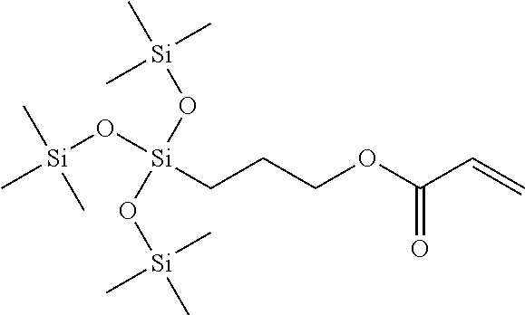
- 3-acryloxypropyltris(trimethylsiloxy)silane (SiM3):
-
- (methacryloxymethyl)bis(trimethylsiloxy)methylsilane (SiM4):
-
- 3-methacryloxypropylbis(trimethylsiloxy)methylsilane (SiM5):
-

- (3-acryloxypropyl)methylbis(trimethylsiloxy)silane (SiM6):
-
- methacryloxypropyltris(trimethylsiloxy)silane (SiM7):
-

- acryloxymethyltrimethylsilane (SiM8):
-

- acryloxymethyltris(trimethylsiloxy)silane (SiM9):
-

- or 1,3-bis[(acryloxymethyl)phenethyl]tetramethyldisiloxane (SiM10):
-
- The photocurable composition of the present disclosure can be designed of having a low viscosity before curing. In one embodiment, the viscosity of the curable composition can be not greater than 30 mPa·s, or not greater than 25 mPa·s, or not greater than 20 mPa·s, or not greater than 15 mPa·s, or not greater than 10 mPa·s. In another certain embodiment, the viscosity may be at least 5 mPa·s. In a particularly preferred aspect, the photocurable composition can have a viscosity from 5 mPa·s to not greater than 20 mPa·s. As used herein, all viscosity values relate to viscosities measured at a temperature of 23° C. with the Brookfield method using a Brookfield Viscometer.
- In one embodiment, the polymerizable material of photocurable composition can further include at least one polymerizable monomer not containing silicon, such as one or more mono-functional and/or one or more multi-functional polymerizable monomers.
- In one aspect, the polymerizable monomer not containing silicon can include an acrylate monomer. As used herein the term acrylate monomer relates to both unsubstituted and alkyl-substituted acrylates, for example, methacrylate. Non-limiting examples of acrylate monomers can be benzylacrylate (BA), isobornyl acrylate (IBOA), 1,5-pentanediol diacrylate (MPDA), dihydrodicyclopentadienyl acrylate (DCPA), tricyclodecane dimethanol diacrylate (A-DCP), 2-Propenoic acid, 1-phenyl-1,2-ethanediyl ester (or phenyl ethanediol diacrylate) (PHEDA), bisphenol A dimethacrylate, m-xylylene diacrylate, neopentyl glycol diacrylate, or any combination thereof.
- In a further aspect, the amount of the at least one monomer not including silicon can be at least 5 wt % based on the total weight of the polymerizable material, or at least 10 wt %, or at least 15 wt %, or at least 20 wt %, or at least 25 wt %. In another aspect, the amount of monomer not including silicon may be not greater than 40 wt % based on the total weight of the polymerizable material, or not greater than 35 wt %, or not greater than 30 wt %, or not greater than 25 wt %, or not greater than 20 wt %.
- The amount of polymerizable material in the photocurable composition can be at least 50 wt % based on the total weight of the photocurable composition, such as at least 60 wt %, at least 70 wt %, or at least 80 wt %, or at least 90 wt %, or at least 95 wt %. In another aspect, the amount of polymerizable material may be not greater than 99 wt %, such as not greater than 97 wt %, not greater than 95 wt %, not greater than 90 wt %, not greater than 85 wt %, or not greater than 80 wt %, or not greater than 70 wt %. The amount of the polymerizable material can be a value between any of the minimum and maximum values noted above. In a particular aspect, the amount of the polymerizable material can be at least 70 wt % and not greater than 98 wt %.
- In one embodiment, the photocurable composition of the present disclosure can be essentially free of a solvent. As used herein, if not indicated otherwise, the term solvent relates to a compound which can dissolve or disperse the polymerizable monomers but does not itself polymerize during the photo-curing of the photocurable composition. The term “essentially free of a solvent” means herein an amount of solvent being not greater than 5 wt % based on the total weight of the photocurable composition. In a certain particular aspect, the amount of the solvent can be not greater than 3 wt %, not greater than 2 wt %, not greater than 1 wt % based on the total weight or the photocurable composition, or the photocurable composition can be free of a solvent, except for unavoidable impurities.
- In another particular aspect, the photocurable composition can include a solvent in an amount of at least 5 wt % based on the total weight of the photocurable composition, or at least 8 wt %, at least 10 wt %, at least 15 wt %, or at least 20 wt %. In another aspect the amount of solvent may be not greater than 30 wt %, or not greater than 20 wt %, or not greater than 15 wt %, or not greater than 10 wt %, or not greater than 5 wt %, or not greater than 3 wt % based on the total weight of the photocurable composition.
- In order to initiate the photo-curing of the composition if exposed to light, one or more photoinitiators can be included in the photocurable composition. In a certain aspect, the curing can be also conducted by a combination of light and heat curing.
- The photocurable composition can further contain one or more optional additives. Non-limiting examples of optional additives can be stabilizers, dispersants, solvents, surfactants, inhibitors or any combination thereof.
- The photocurable composition of the present disclosure can be adapted for use in inkjet adaptive planarization (IAP) or in nanoimprint lithography (NIL).
- In one embodiment, the photocurable composition can be applied on a substrate to form a photo-cured layer. As used herein, the combination of substrate and photo-cured layer overlying the substrate is called a laminate.
- It has been surprisingly observed that the photocurable composition of the present disclosure can be adapted that a photo-cured layer formed from the photocurable composition may have a high etch resistance. High etch resistance is an important property of resist materials in the fields of nanoimprint lithography (NIL) and inkjet adaptive planarization (IAP). For example, in order to obtain a good pattern transfer in the sub-100 nm range, or even less 20 nm, a high etch resistance is desired. The photocurable composition can combine a high etch resistance with a low viscosity, fast curing rate, and a good strength of the resist after curing. Moreover, a stability of the photocurable composition (no unwanted curing reactions) can be observed for at least three months.
- The present disclosure is further directed to a method of forming a photo-cured layer. The method can comprise applying a layer of the photocurable composition described above on the surface of a substrate, bringing the photocurable composition into contact with a template or superstrate; irradiating the photocurable composition with light to form a photo-cured layer; and removing the template or the superstrate from the photo-cured layer.
- The substrate and the solidified layer may be subjected to additional processing, for example, an etching process, to transfer an image into the substrate that corresponds to the pattern in one or both of the solidified layer and/or patterned layers that are underneath the solidified layer. The substrate can be further subjected to known steps and processes for device (article) fabrication, including, for example, curing, oxidation, layer formation, deposition, doping, planarization, etching, formable material removal, dicing, bonding, and packaging, and the like.
- The photo-cured layer may be further used as an interlayer insulating film of a semiconductor device, such as LSI, system LSI, DRAM, SDRAM, RDRAM, or D-RDRAM, or as a resist film used in a semiconductor manufacturing process.
- The following non-limiting examples illustrate the concepts as described herein.
- Photocurable compositions.
- Photocurable compositions were prepared including the following silicon-containing monomers in varying combinations and amounts: methacryloxymethyltris(trimethyl siloxane)silane (SiM1), 1,3-bis(3-methacryl oxypropyl)tetrakis(trimethylsiloxy)disiloxane (SiM2), and 3-acryloxypropyl-tris(trimethylsiloxy)silane (SiM3). Furthermore, the following polymerizable monomers which do not contain silicon were used in the compositions: dihydrodicyclopentadienyl acrylate (DCPA), benzyl acrylate (BZA), dipentaerythritol penta/hexa acrylate (DPHA), tricyclodecane dimethanol diacrylate (A-DCP), and 1-phenyl-1,2-ethanediyl ester (PHEDA). A detailed summary of the polymerizable monomers for each composition is shown in Table 1.
- The photocurable compositions further contained one or more photoinitiators and surfactants, of which the types and amounts are also summarized in Table 1.
-
TABLE 1 Ingredient S1 S2 S3 C1 C2 C3 C4 C6 C7 SiM2 50 50 25 50 SiM1 50 75 50 50 50 50 SiM3 50 50 DCPA 25 25 BA 25 25 25 25 10 A-DCP 25 25 25 PHEDA 25 25 DPHPA 15 Irgacure 1 1 1 TPO Irgacure 3 3 3 4265 Irgacure 2 2 2 2 2 2 907 FSKM2 3 3 3 3 2 2 2 3 3 FSKM1 0.5 0.5 2 2 2 Si [%] 26.5 26.0 27.4 14.2 12.3 14.2 13.7 14.2 14.2 Viscosity 6.9 11.6 4.5 6.1 8.6 6.4 9.5 4.8 5.9 [mPa · s] - Dry Etch Resistance
- Photo-cured films for testing the etch resistance were made by printing a resist film on a silicon wafer using a J-FIL Imprint Tool I300, whereby the film was fully cured during UV exposure. The thickness of the resist film after curing was about 100 nm.
- For measuring the etch resistance, dry etching under oxygen/argon atmosphere was conducted using a Trion Oracle 3-Chamber Cluster System as etch tool. Two different dry etch chemistries have been tested: 1) etching with an oxygen/argon gas combination (O2/Ar); and 2) etching with a combination of chlorine gas and oxygen (Cl2/O2).
- The following etch conditions were applied.
- O2/Ar—etching: O2: 2 sccm; Argon: 10 sccm; RF power: 45 Watt; pressure: 10 mTorr; etch time: 72 seconds; ICP: 0 Watt.
- Cl2/O2—etching: Cl2: 54 sccm; O2: 9 sccm; RF power: 90 Watt; pressure: 150 mTorr; etch time: 90 seconds; ICP: 0 Watt.
- Table 2 shows the measured etch rates converted to nm/minute for photo-cured samples S1 (made with resist composition containing 26.5 wt % silicon), C1 (made with resist composition containing 14.2 wt % silicon), and C8 (made with resist composition not containing any silicon). Comparative composition C8 contained 36 parts of IBOA, 21 parts of DCPA, 24 parts of BZA and 20 parts of SR247 (crosslinker), together with 3 parts of photoinitiators (1 part of Irgacure 907+2 parts of Irgacure 651 from BASF, USA), 4 parts of surfactant (2.7 parts of FS2000M1 and 1.4 parts of FS2000M2), which was added as a release agent. Composition C8 had a viscosity of 7.0 mPa s at 23° C.
- It can be seen that sample S1 had the best etch resistance for both etching chemistries, O2/Ar and Cl2/O2 etching. A lower content of Si, as in sample C1, led to a lower etch resistance compared to sample S1. The lowest etch resistance (corresponding to the highest etch rate) was observed for sample C8, which did not contain any silicon.
-
TABLE 2 Etch rate [nm/min] Sample O2/Ar Cl2/O2 S1 7.8 9.9 C1 12.4 15.0 C8 52.6 / 58.4 19.9 / 19.5 - Viscosities
- The viscosities measured for all samples shown in Table 1 show that even the representative samples S1, S2, and S3 have very low viscosities, even below 10 mPa·s.
- The viscosities were measured at 23° C., using a Brookfield Viscometer LVDV-II+Pro at 200 rpm, with a spindle size #18. For the viscosity testing, about 6-7 mL of sample liquid was added into the sample chamber, enough to cover the spindle head. For all viscosity testing, at least three measurements were conducted and an average value was calculated.
- Silicon Content Calculation
- The silicon content of the polymerizable material of the photocurable compositions was calculated according to the following equation: Si[wt %]=[Σwi (niMsi)/Mi)]×100% , with Msi being the molecular weight of silicon, Mi being the molecular weight of the respective complete monomer, ni the mol amount of Si in the respective monomer, wi the mol amount of the respective monomer in the complete composition, e.g. wi=0.5 means that the respective monomer contributes to 50 wt % in the composition.
- The specification and illustrations of the embodiments described herein are intended to provide a general understanding of the structure of the various embodiments. The specification and illustrations are not intended to serve as an exhaustive and comprehensive description of all of the elements and features of apparatus and systems that use the structures or methods described herein. Separate embodiments may also be provided in combination in a single embodiment, and conversely, various features that are, for brevity, described in the context of a single embodiment, may also be provided separately or in any subcombination. Further, reference to values stated in ranges includes each and every value within that range. Many other embodiments may be apparent to skilled artisans only after reading this specification. Other embodiments may be used and derived from the disclosure, such that a structural substitution, logical substitution, or another change may be made without departing from the scope of the disclosure. Accordingly, the disclosure is to be regarded as illustrative rather than restrictive.
Claims (20)


Priority Applications (6)
| Application Number | Priority Date | Filing Date | Title |
|---|---|---|---|
| US18/062,374 US20240199816A1 (en) | 2022-12-06 | 2022-12-06 | Photocurable composition with high silicon content |
| TW112136560A TW202424022A (en) | 2022-12-06 | 2023-09-25 | Photocurable composition with high silicon content |
| JP2025527826A JP2025540644A (en) | 2022-12-06 | 2023-11-20 | Photocurable compositions with high silicon content |
| CN202380083468.9A CN120303324A (en) | 2022-12-06 | 2023-11-20 | Photocurable composition with high silicon content |
| KR1020257019090A KR20250107239A (en) | 2022-12-06 | 2023-11-20 | Photocurable composition having high silicon content |
| PCT/US2023/080472 WO2024123531A1 (en) | 2022-12-06 | 2023-11-20 | Photocurable composition with high silicon content |
Applications Claiming Priority (1)
| Application Number | Priority Date | Filing Date | Title |
|---|---|---|---|
| US18/062,374 US20240199816A1 (en) | 2022-12-06 | 2022-12-06 | Photocurable composition with high silicon content |
Publications (1)
| Publication Number | Publication Date |
|---|---|
| US20240199816A1 true US20240199816A1 (en) | 2024-06-20 |
Family
ID=91380056
Family Applications (1)
| Application Number | Title | Priority Date | Filing Date |
|---|---|---|---|
| US18/062,374 Pending US20240199816A1 (en) | 2022-12-06 | 2022-12-06 | Photocurable composition with high silicon content |
Country Status (6)
| Country | Link |
|---|---|
| US (1) | US20240199816A1 (en) |
| JP (1) | JP2025540644A (en) |
| KR (1) | KR20250107239A (en) |
| CN (1) | CN120303324A (en) |
| TW (1) | TW202424022A (en) |
| WO (1) | WO2024123531A1 (en) |
Family Cites Families (5)
| Publication number | Priority date | Publication date | Assignee | Title |
|---|---|---|---|---|
| US7122482B2 (en) * | 2003-10-27 | 2006-10-17 | Molecular Imprints, Inc. | Methods for fabricating patterned features utilizing imprint lithography |
| EP2432821B1 (en) * | 2009-05-22 | 2017-08-30 | Novartis AG | Actinically-crosslinkable siloxane-containing copolymers |
| WO2012147828A1 (en) * | 2011-04-27 | 2012-11-01 | 富士フイルム株式会社 | Curable composition for imprinting, pattern formation method, and pattern |
| US20150252125A1 (en) * | 2014-03-10 | 2015-09-10 | Cheil Industries Inc. | Curable resin compositions and barrier stacks including the same |
| US10996491B2 (en) * | 2018-03-23 | 2021-05-04 | Johnson & Johnson Vision Care, Inc. | Ink composition for cosmetic contact lenses |
-
2022
- 2022-12-06 US US18/062,374 patent/US20240199816A1/en active Pending
-
2023
- 2023-09-25 TW TW112136560A patent/TW202424022A/en unknown
- 2023-11-20 KR KR1020257019090A patent/KR20250107239A/en active Pending
- 2023-11-20 JP JP2025527826A patent/JP2025540644A/en active Pending
- 2023-11-20 WO PCT/US2023/080472 patent/WO2024123531A1/en not_active Ceased
- 2023-11-20 CN CN202380083468.9A patent/CN120303324A/en active Pending
Also Published As
| Publication number | Publication date |
|---|---|
| KR20250107239A (en) | 2025-07-11 |
| CN120303324A (en) | 2025-07-11 |
| WO2024123531A1 (en) | 2024-06-13 |
| JP2025540644A (en) | 2025-12-16 |
| TW202424022A (en) | 2024-06-16 |
Similar Documents
| Publication | Publication Date | Title |
|---|---|---|
| US20070065757A1 (en) | Photo-curable resin composition and a method for forming a pattern using the same | |
| KR102809445B1 (en) | Photocurable composition | |
| KR20100004052A (en) | Curable composition for nanoimprint, cured material thereof and method for producing same, and element of liquid crystal display | |
| JP2025503368A (en) | Photocurable compositions having improved thermal stability | |
| TWI885350B (en) | Photocurable composition | |
| CN105210174A (en) | Imprint material | |
| US20240199816A1 (en) | Photocurable composition with high silicon content | |
| TW202043310A (en) | Curable composition for imprinting, kit, method for manufacturing pattern, and method for manufacturing semiconductor element | |
| TWI891412B (en) | Photocurable composition | |
| CN109071693B (en) | Resin composition for high refractive index cured film formation | |
| KR20100004055A (en) | Curable composition for nanoimprint and cured material using the same and member for liquid crystal display device | |
| TWI770237B (en) | Curable composition for imprint, cured product, pattern manufacturing method, lithography method, pattern, mask for lithography, and polymeric composition for imprint | |
| JPWO2023129311A5 (en) | ||
| US20250084269A1 (en) | Thermal-curable composition for inkjet adaptive planarization | |
| US12247133B2 (en) | Photocurable composition including a reactive polymer | |
| US11261267B1 (en) | Photocurable composition | |
| US20240052183A1 (en) | Photocurable composition | |
| KR102887149B1 (en) | Method of forming a photo-cured layer | |
| US12428508B2 (en) | Photocurable composition including a non-reactive polymer | |
| US20220185915A1 (en) | Curable composition for making cured layer with high thermal stability | |
| CN116547321A (en) | Photopolymerizable composition, optical member formed therefrom, and display device | |
| KR20250161011A (en) | photocurable composition | |
| WO2025216873A1 (en) | Photocurable composition comprising anti-blocking agent |
Legal Events
| Date | Code | Title | Description |
|---|---|---|---|
| AS | Assignment |
Owner name: CANON KABUSHIKI KAISHA, JAPAN Free format text: ASSIGNMENT OF ASSIGNORS INTEREST;ASSIGNORS:WAN, FEN;LIU, WEIJUN;REEL/FRAME:061999/0323 Effective date: 20221201 |
|
| STPP | Information on status: patent application and granting procedure in general |
Free format text: DOCKETED NEW CASE - READY FOR EXAMINATION |
|
| STPP | Information on status: patent application and granting procedure in general |
Free format text: NON FINAL ACTION COUNTED, NOT YET MAILED |
|
| STPP | Information on status: patent application and granting procedure in general |
Free format text: NON FINAL ACTION MAILED |
|
| STPP | Information on status: patent application and granting procedure in general |
Free format text: RESPONSE TO NON-FINAL OFFICE ACTION ENTERED AND FORWARDED TO EXAMINER |
|
| STPP | Information on status: patent application and granting procedure in general |
Free format text: NOTICE OF ALLOWANCE MAILED -- APPLICATION RECEIVED IN OFFICE OF PUBLICATIONS Free format text: ALLOWED -- NOTICE OF ALLOWANCE NOT YET MAILED |
|
| STPP | Information on status: patent application and granting procedure in general |
Free format text: NOTICE OF ALLOWANCE MAILED -- APPLICATION RECEIVED IN OFFICE OF PUBLICATIONS |