US20020034710A1 - Structured screens for controlled spreading of light - Google Patents
Structured screens for controlled spreading of light Download PDFInfo
- Publication number
- US20020034710A1 US20020034710A1 US09/918,408 US91840801A US2002034710A1 US 20020034710 A1 US20020034710 A1 US 20020034710A1 US 91840801 A US91840801 A US 91840801A US 2002034710 A1 US2002034710 A1 US 2002034710A1
- Authority
- US
- United States
- Prior art keywords
- microstructures
- predetermined
- microstructure
- screen
- probability density
- Prior art date
- Legal status (The legal status is an assumption and is not a legal conclusion. Google has not performed a legal analysis and makes no representation as to the accuracy of the status listed.)
- Granted
Links
- 230000007480 spreading Effects 0.000 title claims abstract description 28
- 238000003892 spreading Methods 0.000 title claims abstract description 28
- 238000009826 distribution Methods 0.000 claims abstract description 15
- 238000000034 method Methods 0.000 claims description 61
- 239000000758 substrate Substances 0.000 claims description 25
- 230000003287 optical effect Effects 0.000 claims description 24
- 238000004364 calculation method Methods 0.000 claims description 4
- 229920002120 photoresistant polymer Polymers 0.000 claims description 3
- 238000009792 diffusion process Methods 0.000 abstract description 40
- 230000000694 effects Effects 0.000 description 25
- 238000003491 array Methods 0.000 description 24
- 210000004027 cell Anatomy 0.000 description 22
- 238000005286 illumination Methods 0.000 description 17
- 238000013461 design Methods 0.000 description 12
- 238000004519 manufacturing process Methods 0.000 description 11
- 230000000007 visual effect Effects 0.000 description 10
- 230000008569 process Effects 0.000 description 9
- 230000000737 periodic effect Effects 0.000 description 8
- 238000007493 shaping process Methods 0.000 description 7
- 238000005315 distribution function Methods 0.000 description 6
- 230000003595 spectral effect Effects 0.000 description 6
- 238000013459 approach Methods 0.000 description 4
- 239000005337 ground glass Substances 0.000 description 4
- 230000003993 interaction Effects 0.000 description 4
- 238000009827 uniform distribution Methods 0.000 description 4
- 230000008901 benefit Effects 0.000 description 3
- 238000009499 grossing Methods 0.000 description 3
- 230000004807 localization Effects 0.000 description 3
- 239000000463 material Substances 0.000 description 3
- 238000012545 processing Methods 0.000 description 3
- 238000005070 sampling Methods 0.000 description 3
- 239000012141 concentrate Substances 0.000 description 2
- 230000001627 detrimental effect Effects 0.000 description 2
- 238000011161 development Methods 0.000 description 2
- 238000010586 diagram Methods 0.000 description 2
- 238000012986 modification Methods 0.000 description 2
- 230000004048 modification Effects 0.000 description 2
- 229920000642 polymer Polymers 0.000 description 2
- 230000009467 reduction Effects 0.000 description 2
- 239000007787 solid Substances 0.000 description 2
- 210000004460 N cell Anatomy 0.000 description 1
- NIXOWILDQLNWCW-UHFFFAOYSA-N acrylic acid group Chemical group C(C=C)(=O)O NIXOWILDQLNWCW-UHFFFAOYSA-N 0.000 description 1
- 230000002730 additional effect Effects 0.000 description 1
- 238000005266 casting Methods 0.000 description 1
- 230000001413 cellular effect Effects 0.000 description 1
- 230000001427 coherent effect Effects 0.000 description 1
- 239000003086 colorant Substances 0.000 description 1
- 230000000295 complement effect Effects 0.000 description 1
- 238000000748 compression moulding Methods 0.000 description 1
- 238000012937 correction Methods 0.000 description 1
- 230000007547 defect Effects 0.000 description 1
- 230000001419 dependent effect Effects 0.000 description 1
- 238000001514 detection method Methods 0.000 description 1
- 230000008034 disappearance Effects 0.000 description 1
- 239000006185 dispersion Substances 0.000 description 1
- 238000006073 displacement reaction Methods 0.000 description 1
- 238000005530 etching Methods 0.000 description 1
- 239000012467 final product Substances 0.000 description 1
- 239000011521 glass Substances 0.000 description 1
- 238000000265 homogenisation Methods 0.000 description 1
- 239000007924 injection Substances 0.000 description 1
- 238000001746 injection moulding Methods 0.000 description 1
- 230000010354 integration Effects 0.000 description 1
- 238000010849 ion bombardment Methods 0.000 description 1
- 238000005342 ion exchange Methods 0.000 description 1
- 230000001788 irregular Effects 0.000 description 1
- 239000004973 liquid crystal related substance Substances 0.000 description 1
- 238000002844 melting Methods 0.000 description 1
- 230000008018 melting Effects 0.000 description 1
- 238000005457 optimization Methods 0.000 description 1
- 230000010355 oscillation Effects 0.000 description 1
- 238000001020 plasma etching Methods 0.000 description 1
- 230000010076 replication Effects 0.000 description 1
- 229910052710 silicon Inorganic materials 0.000 description 1
- 239000010703 silicon Substances 0.000 description 1
- 238000001228 spectrum Methods 0.000 description 1
- 238000012360 testing method Methods 0.000 description 1
- 238000012546 transfer Methods 0.000 description 1
- 238000013519 translation Methods 0.000 description 1
- 230000014616 translation Effects 0.000 description 1
Images


Classifications
-
- G—PHYSICS
- G02—OPTICS
- G02B—OPTICAL ELEMENTS, SYSTEMS OR APPARATUS
- G02B3/00—Simple or compound lenses
- G02B3/02—Simple or compound lenses with non-spherical faces
- G02B3/04—Simple or compound lenses with non-spherical faces with continuous faces that are rotationally symmetrical but deviate from a true sphere, e.g. so called "aspheric" lenses
-
- G—PHYSICS
- G02—OPTICS
- G02B—OPTICAL ELEMENTS, SYSTEMS OR APPARATUS
- G02B5/00—Optical elements other than lenses
- G02B5/02—Diffusing elements; Afocal elements
-
- G—PHYSICS
- G02—OPTICS
- G02B—OPTICAL ELEMENTS, SYSTEMS OR APPARATUS
- G02B3/00—Simple or compound lenses
- G02B3/0006—Arrays
- G02B3/0037—Arrays characterized by the distribution or form of lenses
- G02B3/0043—Inhomogeneous or irregular arrays, e.g. varying shape, size, height
-
- G—PHYSICS
- G02—OPTICS
- G02B—OPTICAL ELEMENTS, SYSTEMS OR APPARATUS
- G02B3/00—Simple or compound lenses
- G02B3/0006—Arrays
- G02B3/0037—Arrays characterized by the distribution or form of lenses
- G02B3/0056—Arrays characterized by the distribution or form of lenses arranged along two different directions in a plane, e.g. honeycomb arrangement of lenses
-
- G—PHYSICS
- G02—OPTICS
- G02B—OPTICAL ELEMENTS, SYSTEMS OR APPARATUS
- G02B3/00—Simple or compound lenses
- G02B3/0006—Arrays
- G02B3/0037—Arrays characterized by the distribution or form of lenses
- G02B3/0062—Stacked lens arrays, i.e. refractive surfaces arranged in at least two planes, without structurally separate optical elements in-between
- G02B3/0068—Stacked lens arrays, i.e. refractive surfaces arranged in at least two planes, without structurally separate optical elements in-between arranged in a single integral body or plate, e.g. laminates or hybrid structures with other optical elements
-
- G—PHYSICS
- G02—OPTICS
- G02B—OPTICAL ELEMENTS, SYSTEMS OR APPARATUS
- G02B3/00—Simple or compound lenses
- G02B3/02—Simple or compound lenses with non-spherical faces
- G02B3/08—Simple or compound lenses with non-spherical faces with discontinuous faces, e.g. Fresnel lens
-
- G—PHYSICS
- G02—OPTICS
- G02B—OPTICAL ELEMENTS, SYSTEMS OR APPARATUS
- G02B5/00—Optical elements other than lenses
- G02B5/02—Diffusing elements; Afocal elements
- G02B5/0205—Diffusing elements; Afocal elements characterised by the diffusing properties
- G02B5/021—Diffusing elements; Afocal elements characterised by the diffusing properties the diffusion taking place at the element's surface, e.g. by means of surface roughening or microprismatic structures
- G02B5/0215—Diffusing elements; Afocal elements characterised by the diffusing properties the diffusion taking place at the element's surface, e.g. by means of surface roughening or microprismatic structures the surface having a regular structure
-
- G—PHYSICS
- G02—OPTICS
- G02B—OPTICAL ELEMENTS, SYSTEMS OR APPARATUS
- G02B5/00—Optical elements other than lenses
- G02B5/02—Diffusing elements; Afocal elements
- G02B5/0205—Diffusing elements; Afocal elements characterised by the diffusing properties
- G02B5/021—Diffusing elements; Afocal elements characterised by the diffusing properties the diffusion taking place at the element's surface, e.g. by means of surface roughening or microprismatic structures
- G02B5/0221—Diffusing elements; Afocal elements characterised by the diffusing properties the diffusion taking place at the element's surface, e.g. by means of surface roughening or microprismatic structures the surface having an irregular structure
-
- G—PHYSICS
- G02—OPTICS
- G02B—OPTICAL ELEMENTS, SYSTEMS OR APPARATUS
- G02B5/00—Optical elements other than lenses
- G02B5/02—Diffusing elements; Afocal elements
- G02B5/0205—Diffusing elements; Afocal elements characterised by the diffusing properties
- G02B5/0252—Diffusing elements; Afocal elements characterised by the diffusing properties using holographic or diffractive means
-
- G—PHYSICS
- G02—OPTICS
- G02B—OPTICAL ELEMENTS, SYSTEMS OR APPARATUS
- G02B5/00—Optical elements other than lenses
- G02B5/02—Diffusing elements; Afocal elements
- G02B5/0268—Diffusing elements; Afocal elements characterized by the fabrication or manufacturing method
-
- G—PHYSICS
- G02—OPTICS
- G02B—OPTICAL ELEMENTS, SYSTEMS OR APPARATUS
- G02B5/00—Optical elements other than lenses
- G02B5/02—Diffusing elements; Afocal elements
- G02B5/0273—Diffusing elements; Afocal elements characterized by the use
- G02B5/0278—Diffusing elements; Afocal elements characterized by the use used in transmission
-
- G—PHYSICS
- G02—OPTICS
- G02B—OPTICAL ELEMENTS, SYSTEMS OR APPARATUS
- G02B5/00—Optical elements other than lenses
- G02B5/18—Diffraction gratings
- G02B5/1866—Transmission gratings characterised by their structure, e.g. step profile, contours of substrate or grooves, pitch variations, materials
- G02B5/1871—Transmissive phase gratings
-
- Y—GENERAL TAGGING OF NEW TECHNOLOGICAL DEVELOPMENTS; GENERAL TAGGING OF CROSS-SECTIONAL TECHNOLOGIES SPANNING OVER SEVERAL SECTIONS OF THE IPC; TECHNICAL SUBJECTS COVERED BY FORMER USPC CROSS-REFERENCE ART COLLECTIONS [XRACs] AND DIGESTS
- Y10—TECHNICAL SUBJECTS COVERED BY FORMER USPC
- Y10S—TECHNICAL SUBJECTS COVERED BY FORMER USPC CROSS-REFERENCE ART COLLECTIONS [XRACs] AND DIGESTS
- Y10S430/00—Radiation imagery chemistry: process, composition, or product thereof
- Y10S430/146—Laser beam
Definitions
- the present invention discloses an optical device composed of a substrate whose surface or surfaces, which may be flat or curved, contain a distribution of microstructures capable of spreading (also referred to herein as “diffusing” or “scattering”) an incident beam over a controlled range of angles and with controllable intensity variation across the useful field.
- the said device is referred to herein as a “structured screen” or simply a “screen.”
- the structured screens of the invention have a plurality of applications which generally fall into two major categories, namely, diffusive screens and display screens. More particularly, applications of the structured screens include, but are not limited to, homogenization of illumination, in conjunction with or as a focusing screen for photographic cameras, to provide uniform illumination over specific viewing angles, and applications in back-lit displays, liquid crystal flat panel displays, and other types of displays either as a standalone device or in conjunction with other necessary hardware.
- Examples of instruments where the structured screens can be used include, but are not limited to, photographic cameras, computer screens, television sets, projection screens, cellular phones, and general image display equipment.
- a diffusive screen is made of a rough surface with a relief pattern that can be typically described by Gaussian statistics.
- Gaussian statistics To fabricate such diffusive screens several methods have been proposed. Among these one can distinguish three basic categories.
- a second class of diffusive screens is obtained by holographic recording of a speckle pattern.
- This class offers more flexibility than ground glass screens in tailoring the diffusion pattern.
- holographic diffusive screens tend to generate images with a grainy appearance, which may be unpleasant for viewing purposes.
- the sudden intensity variations associated with speckles lead to non-uniform illumination over restricted viewing angles.
- the third class of diffusive screens include those where a certain substrate has its surface modified according to some relief pattern.
- An example includes arrays of microlenses which provide light diffusion. This third class offers better control of the relief pattern than either ground glass screens or holographic screens.
- U.S. Pat. No. 4,427,265 discloses a diffusive screen with an irregular arrangement of curved surfaces superposed on a periodic microlens array. The goal is to maintain the light diffusing properties while avoiding some of the artifacts associated with the underlying periodic array. The curvature of each microlens is controlled on average.
- U.S. Pat. No. 5,733,710 describes various arrangements of microlenses generated by mask exposure with microlens location being varied through mask rotation. It also discloses the combination of a diffusive screen structure and a Fresnel lens on opposite sides of the same substrate.
- U.S. Pat. No. 4,826,292 discloses a diffusion plate with a relief structure composed of cones created by ion bombardment and etching.
- U.S. Pat. No. 5,871,653 discloses fabrication methods to obtain a diffusive screen structure based on microlens arrays for use in flat panel displays.
- Some of the issues that must be addressed when designing a diffusive screen include controllable viewing angles, controllable intensity variation over the useful viewing field, resolution, absence of visual artifacts, and efficient use of the incident illumination. To achieve full control of design capabilities and obtain the best possible diffusing performance for a given application one must be able to control the surface-relief pattern with adequate precision.
- the quality obtained in the prior art is a largely statistical process because there has been no strict control of the positioning and/or shaping of the structures used to achieve diffusion.
- the elementary structures that compose the arrays are conventionally nearly spherical shapes.
- the elementary structures that compose a diffusive screen are loosely described as “curved” simply because there is little control over their shape.
- the surface is obtained by random means of only statistical control, such as surface bombardment.
- the display screen represents the element of direct contact with the user and, for this reason, needs to embody in the best possible way the performance of the system.
- the display screen provides the immediate impression to the user and the quality of the image it can provide determines, to a great extent, the acceptance or not of a particular system.
- Some of the issues relevant to the performance of display screens are efficiency (brightness), resolution (ability to resolve features and avoid aliasing effects), gain (scattering over specified angular range), low speckle (graininess of image associated with random structures of some screen surface designs), contrast (clear distinction between colors), and ambient light rejection (screen looks black when light engine is turned off). These are just some of the issues that must be taken into account in the design of the light engine, optics, and display screen, since these all work together.
- display screens have incorporated random elements in the screen surface without, however, being able to closely control the shape of the micro-scatterers or the scattering pattern.
- the simplest screens have been in the form of classical ground glass diffusers.
- Other devices have included holographic diffusers and microlens arrays. In most of these cases, some element of randomness has been introduced by the recording of a speckle pattern or by superposing and distributing microlens shapes in a random fashion.
- a key distinction of the invention in relation to the prior art is its ability to finely shape the form of the screen surface and arbitrarily distribute it to within, for example, fractions of a micron as well as position the elementary units relative to each other in a precise and general fashion. Methods based on statistical processes are unable to attain such accuracy and, for that reason, can control the spreading pattern only to a limited degree. Put simply, the precise definition of the light spreading (scattering) pattern produced by a screen depends on the features of the screen. If only limited control is possible over the screen structure, only limited shaping is possible over the resulting scattering.
- the structured relief surface according to the invention is composed of two main aspects, which are the shape of the elementary units and the spatial distribution of such units.
- the particular shape of the elementary units is defined by the required properties of the light spreading.
- the specific shapes can assume many forms including, but not limited to, spherical, parabolic, hyperbolic, piecewise linear, piecewise polynomial, pyramidal, conical or combinations thereof. Specific shapes affect the spreading differently and specific choices can be made that are suitable to the spreading required for any particular application. Combinations of different shapes at different locations on a screen surface can be used if desired.
- the relative spatial arrangement of those units can be defined arbitrarily.
- the arrangement of units follows any specified pattern with a precision of, for example, only a fraction of a micron.
- a key distinction of the present invention in relation to the prior art is its ability to distribute elementary units according to patterns where not only shapes and sizes but also relative locations are distinct.
- the invention provides a method for making a structured screen that provides a desired spread of incident light, said structured screen comprising a substrate and a plurality of microstructures distributed over at least one surface of said substrate, said method comprising:
- step (d) comparing the calculated spread of step (c) with the desired spread and, if necessary, repeating at least one of steps (a) and (b), and step (c) until the comparison between the calculated spread and desired spread satisfies a specified criterion (e.g., angular spread, homogeneity, etc.); and
- step (e) producing a plurality of microstructures having, to an accuracy of better than 10 ⁇ n , the locations and the configurations which, in step (d), resulted in the satisfaction of the specified criterion, where 10 ⁇ n is the nominal operating wavelength for the screen.
- the invention provides apparatus for controlled spreading of light comprising a plurality of microstructures, each microstructure being located with better than 10 ⁇ n accuracy at a predetermined location with respect to all other microstructures and each microstructure having a configuration that corresponds, with better than 10 ⁇ n accuracy, to a predetermined mathematical relation, where ⁇ n is the nominal operating wavelength of the apparatus and said predetermined locations and predetermined mathematical relations allow an a priori calculation of the spreading of incident light by the apparatus.
- the nominal operating wavelength ⁇ n can be, for example, the midpoint of the wavelength range over which the screen (apparatus) will be used or a particular wavelength of interest within such a range.
- the accuracy of the microstructures and their locations is better than 5 ⁇ n , and most preferably better than ⁇ n or fractions thereof.
- this corresponds to a preferred accuracy on the order of a few microns and a most preferred accuracy on a sub-micron (fraction of a micron) level.
- the most preferred level of accuracy for the visible range is referred to at various points in the specification, it being understood that these references are only for the purpose of facilitating the discussion of the invention and are not intended in any way to limit the invention to this level of accuracy.
- s(x,y) is the sag of said portion
- c is its curvature
- (x c , y c ) is its center point
- ⁇ is a conic constant
- a p are aspheric coefficients.
- At least some of the microstructures comprise an anamorphic microlens.
- s(x,y) is the sag of said portion
- (x c , y c ) is its center point
- c x and c y are curvatures along x and y, respectively
- ⁇ x and ⁇ y are conic constants along x and y, respectively
- a xp and A yp are higher order aspheric coefficients along x and y, respectively.
- the first form is generally not used with aspheric coefficients since it couples curvatures and conic constants in x and y.
- microstructures comprise a curved, microlens portion and a straight-sided, piston (cylindrical) portion.
- Microstructures having this microlens-piston structure are themselves an aspect of the invention.
- FIG. 1 schematically illustrates two microstructures constructed in this way, where microstructure 1 has a spherical microlens portion of maximum sag s 1 and a piston portion of diameter d 1 and height (offset) p 1 , and microstructure 2 has a parabolic microlens portion of maximum sag s 2 and a piston portion of diameter d 2 and height (offset) p 2 , with the apices of the two microstructures being separated by a depth D.
- this drawing shows convex microstructures and only two microlens configurations, it being understood that the invention also applies to concave microstructures, combinations of convex and concave microstructures, and microlens configurations of any and all types.
- At least a portion of at least some of the microstructures is selected to have a configuration characterized by at least one parameter with the at least one parameter being randomly distributed in accordance with a predetermined probability density function (e.g., a uniform probability density function over a predetermined range for the parameter).
- a predetermined probability density function e.g., a uniform probability density function over a predetermined range for the parameter.
- radius of curvature ; maximum surface sag; a parameter characteristic of the transverse size of a microstructure (e.g., diameter); for microstructures which comprise a curved, microlens portion and a straight-sided, piston portion (see FIG. 1), the heights of the straight-sided, piston portions; and for microstructures having apices, the distances of the apices from the screen's substrate or, alternatively, where the distances have a maximum value, the differences between the distances and said maximum value.
- a parameter characteristic of the transverse size of a microstructure e.g., diameter
- microstructures which comprise a curved, microlens portion and a straight-sided, piston portion see FIG. 1
- the heights of the straight-sided, piston portions for microstructures having apices, the distances of the apices from the screen's substrate or, alternatively, where the distances have a maximum value, the differences between the distances and said maximum value.
- More than one parameter can be randomized, if desired, with the randomization (e.g., probability density function) being the same or different for the parameters.
- the randomization e.g., probability density function
- one randomly-distributed parameter can characterize the curved, microlens portion and a second randomly-distributed parameter can characterize the straight-sided, piston portion.
- the locations of the microstructures form a regular array (e.g., a hexagonal array). In other embodiments, the locations are based on a set of unit cells which form a mosaic (e.g., a random mosaic).
- the screen can have internal microstructures and edge microstructures, with the mosaic providing at least some junctions between internal microstructures that correspond, in terms of light spreading, to at least some junctions between edge microstructures resulting from the tiling of two screens to one another.
- the locations of the microstructures are randomly distributed in accordance with a predetermined probability density function.
- the locations of the microstructures can be based on a random set of polygonal shaped boundaries.
- the substrate of the screen comprises two spaced-apart (e.g., major) surfaces and the microstructures are distributed over both surfaces.
- microstructures are distributed over one of the surfaces, with the other surface comprising a Fresnel lens.
- the screen's substrate defines a first optical axis and the configuration of at least some of the microstructures comprises a microlens which defines a second optical axis which is not parallel to the first optical axis. Screens having such a configuration are themselves an aspect of the invention.
- the invention provides a structured screen comprising a plurality of predetermined microstructures, wherein:
- microstructures comprise a curved, microlens portion and a straight-sided, piston portion which has a predetermined height which can be zero:
- said curved, microlens portions have predetermined diameters and predetermined maximum sags;
- At least one of the predetermined diameters, the predetermined maximum sags, and the predetermined heights can be randomly distributed in accordance with a predetermined probability density function (e.g., a uniform probability density function over a predetermined range for said diameters, maximum sags, and/or heights).
- a predetermined probability density function e.g., a uniform probability density function over a predetermined range for said diameters, maximum sags, and/or heights.
- the invention provides a structured screen comprising a plurality of predetermined aspherical microlenses (e.g. parabolic microlenses), wherein said microlenses:
- At least one of the predetermined diameters and the predetermined maximum sags can be randomly distributed in accordance with a predetermined probability density function (e.g., a uniform probability density function over a predetermined range for said diameters and/or maximum sags).
- a predetermined probability density function e.g., a uniform probability density function over a predetermined range for said diameters and/or maximum sags.
- the invention provides a structured screen comprising:
- the invention provides a structured screen comprising a plurality of unit cells and a plurality of microstructures, one microstructure associated with each unit cell, wherein the perimeters of the unit cells are non-regular polygons.
- the perimeters can be defined by a predetermined probability density function.
- the invention provides a structured screen comprising a plurality of microstructures at least some of which comprise a microlens having a first curvature in a first direction and a second curvature in a second direction orthogonal to the first direction, at least one of said first and second curvatures being randomly distributed in accordance with a predetermined probability density function.
- both the first and second curvatures are randomly distributed in accordance with a predetermined probability density function which may be the same or different for the two curvatures.
- the invention provides a structured screen comprising:
- a first sub-screen comprising a plurality of internal microstructures and a plurality of edge microstructures, each microstructure being located at a predetermined location with respect to all other microstructures, said predetermined locations being based on a first set of unit cells which form a first mosaic;
- a second sub-screen comprising a plurality of internal microstructures and a plurality of edge microstructures, each microstructure being located at a predetermined location with respect to all other microstructures, said predetermined locations being based on a second set of unit cells which form a second mosaic;
- each of the first and second mosaics provides at least some internal junctions between internal microstructures that correspond, in terms of light spreading, to at least some of the edge junctions.
- each of the first and second mosaics can be random. In other embodiments, the first and second sub-screens are identical.
- FIG. 1 is a schematic drawing illustrating representative microstructures of the invention.
- FIG. 2 shows diffraction patterns due to two periodic arrays of microlenses of depth equal to 24 ⁇ m, calculated using Eq. (2).
- FIG. 3 is a comparison of the elementary units of the arrays used to calculate the diffraction patterns shown in FIG. 1.
- the solid line refers to the aspherical surface with nonzero conic while the dashed line refers to the spherical surface.
- FIG. 4 shows the difference between the spherical and aspherical profile necessary to generate the diffraction pattern shown in FIG. 1.
- FIG. 5 is a calculated diffusion pattern for a regular array of parabolic units.
- FIG. 6 is a calculated diffusion pattern for a random array of parabolic units with variable depth and constant pitch.
- FIG. 7 is a calculated diffusion pattern for a random array of parabolic units with variable depth and variable pitch.
- FIG. 8 is a histogram of radii of curvature for a single realization of a random microlens array having a uniform probability density function for radius of curvature.
- FIG. 9 is a histogram of depth for a single realization of a random microlens array having a uniform probability density function for radius of curvature.
- FIG. 10 is a calculated three-dimensional scattering pattern due to a random microlens array with a hexagonal unit cell structure.
- the probability density function is uniform for radius of curvature.
- FIG. 11 is a histogram of radii of curvature for a single realization of a random microlens array with a uniform probability density function for microlens depth.
- FIG. 12 is a histogram of depth for a single realization of a random microlens array with a uniform probability density function for microlens depth.
- FIG. 13 is a calculated three-dimensional scattering pattern due to a random microlens array with a hexagonal unit cell structure.
- the probability density function is uniform for microlens depth.
- FIG. 14 is a schematic diagram of coordinate systems that can be used to define the spatial localization of elementary structures (microstructures) on one or more surfaces of a screen. For simplicity only a two-dimensional plot is shown.
- the (X,Y) frame denotes a global coordinate system, while the (x,y) frames denote local coordinates associated with individual microstructures.
- FIG. 15 illustrates elementary units arranged on a regular square lattice with each unit (represented by circles) centered on a unit cell (square regions containing circles) and having a size that is no greater than the cell itself.
- the center of a cell is represented by the cross mark.
- FIG. 16 illustrates an arrangement of elementary units on a square lattice of constant fill factor but with centers of individual units displaced with respect to the centers of the unit cells.
- FIG. 17 illustrates an arrangement of elementary units on a square lattice of variable fill factor and with centers of individual units displaced with respect to the centers of the unit cells.
- FIG. 18 illustrates an arrangement of elementary units on a square lattice with 100% fill factor.
- the boundary of each elementary unit is denoted by the dotted line but the unit itself is only defined within the square unit cell.
- the center of individual units may be displaced with respect to the center of the cell.
- FIG. 19 illustrates elementary units arranged on a regular hexagonal lattice with 100% fill factor.
- FIG. 20 illustrates elementary units distributed over a random set of polygonal shaped unit boundaries.
- FIG. 20 illustrates elementary units distributed over a random set of polygonal shaped unit boundaries.
- FIG. 20 illustrates elementary units distributed over a random set of polygonal shaped unit boundaries.
- FIG. 20 illustrates elementary units distributed over a random set of polygonal shaped unit boundaries.
- FIG. 20 illustrates elementary units distributed over a random set of polygonal shaped unit boundaries.
- FIG. 20 illustrates elementary units distributed over a random set of polygonal shaped unit boundaries.
- FIG. 20 illustrates elementary units distributed over a random set of polygonal shaped unit boundaries.
- FIG. 20 illustrates elementary units distributed over a random set of polygonal shaped unit boundaries.
- FIG. 20 illustrates elementary units distributed over a random set of polygonal shaped unit boundaries.
- FIG. 20 illustrates elementary units distributed over a random set of polygonal shaped unit boundaries.
- FIG. 20 illustrates elementary units distributed over a random set of
- FIG. 21 illustrates a structured screen where both surfaces of a substrate of thickness ⁇ are structured with an array of individual elementary units, according to some of the embodiments of the present invention.
- FIG. 22 shows calculated diffraction patterns for diffusive screen arrays composed of triangular elementary units with a vertical offset (solid line) compared to a regular array (dashed line) without such an offset.
- FIG. 23 is a schematic drawing showing an illumination source, a Fresnel lens, and microlens array.
- FIG. 24 is a schematic drawing showing a prior art integration of a screen and a Fresnel lens.
- FIG. 25 is a schematic drawing showing the combination of diffusion and Fresnel collimation on a single surface.
- FIG. 26 shows a calculated scattering pattern for a regular array of spherical microlenses 10- ⁇ m deep for operation in the infrared.
- FIG. 27 shows a calculated scattering pattern for a regular array of triangular microstructures 10- ⁇ m deep for operation in the infrared.
- FIG. 28 shows a calculated scattering pattern for a regular array of hyperbolic microstructures 10- ⁇ m deep for operation in the infrared.
- FIG. 29 shows a calculated scattering pattern for a regular array of spherical microstructures 12- ⁇ m deep for operation in the visible.
- FIG. 30 shows a calculated scattering pattern for a regular array of spherical microstructures 20- ⁇ m deep for operation in the visible.
- FIG. 31 shows a calculated scattering pattern for a regular array of parabolic microstructures 20- ⁇ m deep for operation in the visible.
- FIG. 32 shows a regular array of spherical microlenses (diameter: 100 microns, maximum sag: 10 microns).
- FIG. 33 shows an array of identical spherical microlenses (diameter: 100 microns, maximum sag: 10 microns), with random vertical offset equal to ⁇ 2 microns.
- FIG. 34 shows a calculated scattering profile for an array of identical spherical microlenses of 100 microns diameter and 10 microns maximum sag. Vertical microlens positioning includes a maximum vertical offset of +2 microns.
- FIG. 35 shows calculated scattering patterns for arrays of identical spherical microlenses of diameter 100 microns and maximum sag 10 microns for operation in the visible, with and without a vertical offset of ⁇ 2 microns.
- FIG. 36 illustrates a square arrangement of microstructures.
- FIG. 37 illustrates a hexagonal arrangement of microstructures.
- FIG. 38 illustrates a random arrangement of microstructures delimited by random polygonal boundaries.
- FIG. 39 illustrates a screen with a mosaic spatial arrangement. Note the relative displacement of microlenses and the tiling naturally exhibited by this configuration, i.e., the mosaic has at least some junctions between internal microstructures that correspond, in terms of light spreading, to at least some junctions between edge microstructures which would result from the tiling of two screens to one another.
- FIG. 40 shows frequency of sag and frequency of radius of curvature (PDF uniform in radius of curvature) for a sag range of 5-15 ⁇ m and 100-micron diameter spherical microlenses.
- FIG. 41 shows frequency of sag and frequency of radius of curvature (PDF uniform in sag) for a sag range of 5-15 ⁇ m and 100-micron diameter spherical microlenses.
- FIG. 42 shows calculated scattering patterns which illustrate the effect of a probability distribution function on scattering pattern for an array of random spherical microlenses with a sag range between 5 ⁇ m and 15 ⁇ m.
- the lens diameter is 100 microns and the vertical offset is ⁇ 2 ⁇ m.
- FIG. 43 shows an array of spherical microlenses with a hexagonal arrangement. Each microlens is 0.5 mm in diameter and has a maximum sag in the range 2 to 8 ⁇ m. There is also a vertical offset of ⁇ 2 ⁇ m.
- FIG. 44 shows a calculated three-dimensional scattering pattern obtained with the structured screen shown in FIG. 43.
- FIG. 45 shows cross-sections of the scattering pattern of FIG. 44 along two perpendicular directions.
- FIG. 46 is a calculated scattering pattern for a hexagonal display screen.
- FIG. 47 shows a hexagonal array of anamorphic microlenses (average diameter 50 ⁇ m). The bar indicates microlens depth.
- FIG. 48 shows a calculated scattering pattern for an anamorphic mosaic array.
- FIG. 49 shows a mosaic array of anamorphic microlenses. The bar indicates microlens depth.
- A. Diffraction Equation The structured screens of the invention are designed using diffraction equations appropriate to the conditions under which the finished screen is to be used (near field, far field, with or without focusing lenses, etc.).
- f ⁇ ( u , v ) exp ⁇ ( ikz ) i ⁇ ⁇ ⁇ ⁇ ⁇ z ⁇ ⁇ - ⁇ ⁇ ⁇ ⁇ - ⁇ ⁇ ⁇ exp ⁇ [ ik ⁇ [ n ⁇ ( ⁇ ) - 1 ] ⁇ s ⁇ ( x , y ) - i ⁇ ⁇ 2 ⁇ ⁇ ⁇ ⁇ ⁇ z ⁇ ( xu + yv ) ] ⁇ ⁇ x ⁇ ⁇ y , ( 1 )
- f ⁇ ( u , v ) exp ⁇ ( ikz ) i ⁇ ⁇ ⁇ ⁇ ⁇ z ⁇ ⁇ J ⁇ ⁇ D j ⁇ ⁇ exp ⁇ [ ik ⁇ [ n ⁇ ( ⁇ ) - 1 ] ⁇ s j ⁇ ( x , y ) - i ⁇ ⁇ 2 ⁇ ⁇ ⁇ ⁇ ⁇ z ⁇ ( xu + yv ) ] ⁇ ⁇ x ⁇ ⁇ y . ( 2 )
- the above expression illustrates the significant elements involved in the design of the structured screens of the invention.
- the first element is the shape of individual elements s j (x,y).
- the second is the cell D j , where the individual element is contained.
- the prior art has had limited control over the elementary functions s j (x,y) except to guarantee some amount of focusing power, and the cells have usually been square or hexagonal.
- the present invention improves upon previous approaches by (i) allowing exact definition of the shape s j (x,y) to, for example, a sub-micron accuracy; (ii) allowing precise definition of the spatial localization of the domain of each cell D j relative to any other cell; and (iii) allowing precise definition of the cell shape D j , not limited to only square or hexagonal arrays, but assuming any contour necessary to implement the desired spreading pattern.
- the surface-relief pattern on any one side or on both sides of the structured screen is responsible for the spreading of the incident illumination.
- This pattern achieves the goal of shaping the diffused illumination by a specified arrangement and choice of elementary units, which are generally different from each other and are displaced at specific distances from each other, according to the requirements of the desired beam shaping.
- each elementary unit can be defined in terms of segments characterized by piecewise functions.
- the general shape can assume either a continuous or discontinuous form and can also impart focusing power to the incident illumination.
- the particular shape of each individual element is of fundamental importance in shaping the diffused light.
- the elementary shape is precisely control to tailor the diffusion profile.
- FIG. 2 shows diffusion patterns for of two regular arrays of identical relief depth but with the shape of each elementary unit in one array being different from the shape of each unit in the other array. In both cases the total relief depth is the same. The difference in the patterns is evident in this figure.
- FIG. 3 A comparison between the profiles of each individual shape for the two arrays is shown in FIG. 3, while the difference between the two profiles is shown in FIG. 4. Note that to achieve the kind of diffusion control illustrated by the two curves of FIG. 2, it is necessary to ensure microstructure relief control on the order of, for example, a few microns.
- the grating profile determines the distribution of power among orders.
- a triangular blazed grating can be designed for 100% theoretical efficiency at a single order.
- custom shapes can be obtained that spread the incident illumination over many orders. Such control of the light spread is only possible with proper choice of the elementary shape of the grating.
- Eq. (4) allows a wide variety of shapes to be implemented, it is limited to conic surfaces with aspheric corrections.
- any surface that can be defined by a mathematical relation can be implemented, including mathematical relations based on algorithmic processes.
- the present invention also allows the profile of each micro structure to vary across all or part of an array with each microstructure still being controlled to, for example, sub-micron accuracy. In this way it is possible to homogenize the diffused light and avoid the visual artifacts caused by a periodic array.
- regular arrays has some advantages from a fabrication point of view but the performance of the screen may not be satisfactory due to the introduction of image artifacts such as high- frequency intensity variations. Furthermore, the control of light diffusion is limited because an array in general will not meet all types of system criteria. In some broadband applications, regular arrays may be acceptable because the smoothing by spectral dispersion helps to minimize the image artifacts due to the grating structure.
- FIG. 5 The behavior of a regular array is shown in FIG. 5 for parabolic microlenses of diameter equal to 100 ⁇ m and depth 5 ⁇ m.
- the incident illumination belongs to the 400-700 nm spectral band. One observes that although diffusion is accomplished, high-frequency intensity variations are present and higher-order components are noticeable.
- FIG. 6 shows the diffusion obtained by a regular parabolic array of diameter 100 ⁇ m but with depth randomly chosen in the range 5-10 ⁇ m, averaged over several statistically identical screen configurations.
- the intensity diffusion can be well-described by a fourth-order supergaussian with an angular spread of about 7.7 degrees measured at the 1/e 2 intensity point.
- the randomization avoids the high-frequency structure as well as high order diffraction angles. Note that these calculations assume a spatially coherent beam incident on the aperture. In practice, partial coherence effects would further reduce the intensity fluctuations.
- FIG. 7 shows another diffusion pattern of parabolic units with random depth in the range 5-10 ⁇ m and with the diameter sizes of each unit randomly chosen with a variation in the range ⁇ 20% with respect to the nominal diameter of 100 ⁇ m.
- the main difference with respect to the pattern of FIG. 6 is the elongated tail of Lorentzian shape.
- Control of the diffusion process depends on the particular way microstructures differ from each other. In general, this variability can be expressed in terms of a probability distribution function (PDF) for a particular parameter(s) of choice. For instance, if the array presents microlens structures with random radii of curvature, then there exists a PDF that defines how the radius of curvature varies across the array. Similarly, the PDF might refer to a conic constant, the depth of a given microstructure, the location of a given microstructure, the size of a given microstructure, any combination of these parameters, or any other relevant parameters or combinations thereof.
- PDF probability distribution function
- the PDF can be arbitrarily defined and an array can be accordingly built.
- the exact correspondence between the actual array and the PDF that describes it requires that each elementary microstructure be fabricated with, for example, sub-micron accuracy.
- Methods for specifying a PDF depend largely on the desired properties of the diffusion pattern but can be of either a deterministic or statistical nature.
- the first element is the microstructure itself, which can be of any particular shape, as discussed immediately above.
- the second element is the relative spatial placement of the individual microstructures where each microstructure is spatially placed with respect to each other arbitrarily and with, for example, sub- micron accuracy.
- the global coordinate system can be located arbitrarily with respect to the screen and defines a reference frame from which each microstructure can be localized with respect to some arbitrary reference point such as the vertex, tip, or any other element of the microstructure.
- a local coordinate system is next associated with each microstructure.
- the surface shape of the microstructure can be defined according to a function of the form s(x ⁇ X k ,y ⁇ Y k ), where s denotes the functional form of the microstructure, (x,y) denotes a point in the local coordinate system, and (X k ,Y k ) is the position of the k th local coordinate system with respect to the global reference frame where k runs from 1 to the total number of microstructures present on the screen.
- FIG. 14 A schematic illustration of the two reference frames is shown in FIG. 14, where for simplicity, the two dimensional case is shown, it being understood that the general case is three dimensional.
- microstructure positioning along the surface of the screen or perpendicular to it In relation to the global coordinate system one may distinguish microstructure positioning along the surface of the screen or perpendicular to it. Along the surface, various realizations of this embodiment include regular periodic arrays, random arrays with the distance between neighbor microstructures varying as a function of position, microstructures with well-defined boundaries such as in a square or hexagonal array, microstructures with random boundaries where the size and shape of each microstructure varies as a function of position across the screen, or structures positioned on both surfaces of the screen.
- FIGS. 15 through 21 Examples of possible arrangements are illustrated in FIGS. 15 through 21.
- a random component such component will be defined in terms of a probability density function (PDF).
- PDF probability density function
- each microstructure In the direction perpendicular to the screen surface, there can be a vertical offset of each microstructure with respect to each other, also called piston.
- the presence of piston is relevant in the reduction of high-frequency intensity variations in the diffusion pattern (speckle), as well as in avoiding the presence of hot spots, which are isolated regions of the diffusion pattern that exhibit much higher intensity than the average of the whole pattern.
- the amount of piston used in any particular application will depend on the characteristics of the illumination on the screen but, in general, should be equivalent to a few optical wavelengths of the illumination. Also, the magnitude of the piston component for neighbor microstructures will typically vary randomly according to a PDF, unless it is desirable to introduce some bias in the diffusion pattern.
- FIG. 22 illustrates the effect of a vertical offset on a diffraction pattern for an elementary unit having a triangular shape.
- a regular array having a grating period of 200 ⁇ m and a depth of 5 ⁇ m light of wavelength 0.5 ⁇ m is focused at a diffracted order centered at the angular distance of ⁇ 0.14 degrees with an angular divergence of 0.006 degrees.
- the corresponding diffraction pattern is shown in FIG. 22 by the dashed curve.
- the solid curve is the result of an ensemble average over statistically identical arrays of triangular units with a maximum offset (piston) of 2 ⁇ m.
- the offset obeys a uniform probability distribution function.
- the diffusion attained through the introduction of the offset is more that one order of magnitude. Note however that this level of diffusion is peculiar to the blazed grating that was analyzed. In general, the degree of diffusion is shape-dependent. However, as a general rule, the offset helps in the smoothing of the diffusion pattern, since it helps eliminate artifacts due to the periodic grating structure.
- the distributed microstructures of the invention can be used in combination with or, indeed, can constitute a Fresnel lens, whose purpose is to collimate an otherwise divergent beam of light.
- the function of a Fresnel lens in a structured screen simply requires rotation of individual microstructures having focusing power.
- the individual microlenses have optical axes which are not parallel to the optical axis of the overall screen.
- the optical axis of the screen is typically the optical axis of the screen's substrate.
- a substrate such as glass is covered with, for example, a low-contrast photosensitive polymer (photoresist) that is exposed and records in a latent image the exposure pattern defined by the laser beam.
- a photosensitive polymer photoresist
- the photosensitive material is positive, in which case, when the substrate is developed, the exposed material is eliminated leaving a surface relief structure.
- This surface relief structure basically defines the desired screen surface or, in some cases, its complement. See commonly assigned U.S. patent application Ser. No. 60/222,032 which is being filed concurrently herewith in the names of Geoffrey B. Gretton, G. Michael Morris, and Tasso R. M. Sales, and is entitled “Microlens Arrays Having High Focusing Efficiency,” the contents of which in its entirety is incorporated herein by reference.
- the surface relief structure obtained upon development of the photoresist may not be precisely the desired structure depending on specific performance characteristics of the fabrication process. That is, the fabrication process itself can introduce features that may be undesirable in the final product and need to be accounted for in using the process. For example, since a writing laser beam has a finite size, the final surface after development represents the profile defined by the laser exposure system convolved with the shape of the laser beam used. In some instances the presence of convolution may not be detrimental to the performance of the screen but in other cases it must be avoided. Of course, the performance requirements and operating conditions dictate the fabrication tolerances and limitations.
- the surface relief profile left on the surface of the substrate can serve as a master mold that can be used to obtain a large number of replicas according to several possible techniques including casting on a UV-curable material, injection or compression molding, and reactive ion etching into a substrate.
- a particularly preferred technique for forming the structured screens of the present invention is described in commonly assigned U.S. patent application Ser. No. 09/094,340, filed Jun. 9, 1998, and entitled “Method for Making Optical Micro-Structures Which Can Have Profile Heights Exceeding 15 Microns,” which was published on Dec. 16, 1999 as PCT Patent Publication No. WO 99/64929, the contents of which in their entireties are incorporated herein by reference.
- microstructure shape accuracy and location to within, for example, fractions of a micron can be achieved.
- the structured screens of the present invention can be produced inexpensively and in large volumes.
- the following, non-limiting, examples illustrate the design of structured screens using the techniques discussed above.
- the features of the screen surface or surfaces are controlled with enough precision at each individual location so as to allow the accurate shaping (control) of the light spreading (scattering) pattern in the far field, which is the typical location for an observer.
- the scattering surface is known in detail, it is possible to reliably model its optical behavior using diffraction equations and thus determine the expected performance of the screen as well as the tolerances involved in fabricating the screen.
- the screen itself is composed of micro-elements (microstructures) that act collectively to generate the desired scattering.
- microstructures can be defined by a set of parameters. These are the local components.
- the local parameters could be radii of curvature, conic constants, diameters, and so on.
- the global parameters define the laws that must be obeyed by the local parameters (such as probability distribution functions) and the spatial location of each microstructure with respect to each other.
- each microstructure can employ a conveniently placed coordinate system that defines the center of each microstructure and a global origin. Global components are defined with respect to this coordinate system. At the origin of each microstructure one can also associate a local coordinate system that provides the reference necessary to mathematically define the microstructure. It is through the use of local and global components that one can shape to a virtually unlimited degree the scattering pattern produced by the screen.
- Example 1 illustrates the importance of local degrees of freedom in the shape of the scattering pattern
- Examples 2 and 3 deal with vertical offset and the general spatial placement of microstructures on the screen surface or surfaces, respectively
- Example 4 addresses randomization of screen parameters.
- Examples 5 and 6 present illustrative applications of the invention to the production of diffusing and display screens.
- a microstructure of spherical shape has a sag function that is given by R ⁇ (R 2 ⁇ r 2 ) 1 ⁇ 2 , where R denotes the radius of curvature and r denotes the radial position from the origin.
- the array consists of spherical microlenses with possibly variable radii of curvature.
- the size of each microstructure is identical throughout the screen surface, so that the presence of randomness is confined to a particular parameter, namely, the radii of curvature of the spherical microlenses.
- FIG. 26 shows the far-field scattering profile for an array of spherical microlenses of diameter 100 microns.
- the microlens sag is fixed at 10 microns.
- each microstructure is an isosceles triangle of base 100 microns and depth 10 microns, i.e., the basic dimensions are the same as for the spherical array. Since the array is more akin to a triangular grating one observes the two separated intensity peaks corresponding to the two main diffraction orders.
- FIG. 29 and FIG. 30 illustrate the scattering profile for such an array for two microlens depths, namely, 12 microns in FIG. 29 and 20 microns in FIG. 30.
- microlens depth provides another parameter for shaping the scattering pattern of a screen.
- FIG. 31 The case of a parabolic microlens shape with 20 microns total sag (total depth) is shown in FIG. 31.
- the parabolic profile allows the generation of scattering profiles of considerable flatness (and, as a result, high gain) in comparison with spherical or any other profiles.
- the scattering is virtually identical.
- the microlens sag increases the difference between these two profiles becomes no longer negligible and this reflects directly on the scattering.
- the shape of the microstructure can be used to control the shape of the scattering profile.
- the microstructure profile basically determines the shape and the divergence span of the scattering pattern. Randomizing the profile helps reduce the high-frequency oscillations and attain a smoother pattern. Depending on the spectral band of operation, hot spots may occur that are detrimental to the performance of the screen (see, for example, FIG. 26).
- FIG. 26 To illustrate the effect, we again consider the array used to generate FIG. 26, that is, spherical microlenses of diameter 100 microns and sag 10 microns. Cross-sections of the screen profile without and with piston are shown in FIG. 32 and FIG. 33, respectively. The effect of the offset on the scattering pattern is shown in FIG. 34 which should be compared with the pattern of FIG. 26. The disappearance of the central hot spot is evident in FIG. 34.
- a defining global parameter of great relevance to the scattering pattern is the spatial arrangement of the microstructures on the screen. The main influence of the spatial arrangement is reflected in the overall symmetry of the scattering pattern.
- the regular square array of FIG. 36 generates a three-dimensional pattern that resembles a rectangle, depending on the divergence angles introduced by the local configuration of the microlenses.
- the hexagonal array of FIG. 37 generates a scattering pattern in the form of a hexagon which can be stretched along one direction more than another depending on the divergence angles introduced by the configuration of the microlenses.
- the overall symmetry is important in many aspects, but mainly because it affects how energy is concentrated in the observation plane.
- the hexagonal arrangement of FIG. 37 concentrates more light than the square array of FIG. 36.
- the scattering pattern due to a hexagonal array exhibits more gain, i.e., scattering over a specified angular range, than an equivalent square array.
- the two factors of primary relevance are the shape of the intensity profile and the divergence angle.
- the shape is controlled by the profile of the microstructures (sag function) while the divergence angle is controlled by the slope of the profile (first derivative of the sag function).
- a screen design that renounces a regular spatial arrangement of microstructures. This can be done by employing a screen design where microstructures are characterized by both local parameters and a spatial boundary, where the spatial boundary is the closed line that surrounds the microstructure. For example, for a square array, the boundary is a square, while for a honeycomb, the boundary is a hexagon.
- a regular spatial arrangement can be avoided by using cylinders of variable diameter.
- the boundary can be, in most general form, a polygonal curve.
- the complete set of polygonal curves that defines the boundaries of the microstructures in the whole screen would generally (but not necessarily always) be arranged in close-packed form, as shown in FIG. 38.
- a particular advantage of a mosaic, or a general polygonal boundary is that it reduces the influence of defects caused by the tiling of two or more screen arrays to form a larger screen.
- a particularly effective way to avoid the presence of artifacts due to the periodic repetition of microstructures on a screen is to use randomization, which can be applied to either local parameters or global parameters or to both local and global parameters, as desired.
- PDF probability distribution function
- FIG. 40 and FIG. 41 An illustration of this effect is shown in FIG. 40 and FIG. 41.
- the result of changing the parameter to which the uniform PDF is applied is shown in the scattering patterns of FIG. 42, where the pattern for a uniform PDF in sag is represented by the solid line and that for a uniform PDF in radius of curvature is represented by the dashed line.
- the scattering pattern tends to spread over a larger angular range. This larger angle scattering results from an increased number of deep-sag lens units for the uniform distribution on sag.
- a Gaussian distribution allows the concentration of a parameter (e.g., sag or radius) around a given average value.
- a parameter e.g., sag or radius
- PDF's that can be utilized, the only restrictions being imposed by the desired performance of the system.
- the uniform distribution tends to be the distribution of choice for most applications, mainly due to its simplicity. In many cases of interest this is sufficient to meet the system requirements.
- the option to implement an arbitrary PDF provides an important degree of freedom for tailoring the scattering pattern.
- screens can be divided into two categories, i.e., diffusing screens and display screens, based on the different requirements involved in these two applications.
- an optical detection system might require a larger, homogeneous focal spot for a given spectral band than would be provided without a screen.
- the absence of visual performance requirements typically makes the design of diffusing screens somewhat easier since one must concentrate only on the size and shape of the diffusing pattern.
- the required angular spread tends to be small, which implies the use of shallow microstructures which are easier to fabricate.
- screens for display applications generally present a number of challenges in addition to spreading the illumination into a specific angular range with a certain scattering profile.
- visual requirements e.g., color, contrast, and various subjective variables, involve issues that cannot be easily modeled by diffraction calculations. These are better evaluated by direct observation of a test image on a screen sample.
- a first immediate distinction from diffusive screens is that display screens are confined to the visual part of the spectrum. Another main difference is that displays generally require a larger angular range, typically spanning a total of 100 degrees useful field. In addition, the angular divergence may be different in the vertical and horizontal directions.
- FIG. 46 An example of a scattering pattern for a display screen is shown in FIG. 46.
- the divergence along the fast axis is 36 degrees (estimated gain 4.9) while along the slow axis it is about 17 degrees (estimated gain 16.9).
- This pattern was generated with the hexagonal array of anamorphic microlenses illustrated in FIG. 47.
- FIG. 48 Another example, obtained with an anamorphic mosaic array is shown in FIG. 48, with a portion of the array itself being shown in FIG. 49.
- randomness was introduced for both the individual microlens elements as well as for the sizes of the rectangular boundaries (25 to 30 microns in one direction and 45 to 50 microns in the other).
- the divergence along the fast axis is 33 degrees (estimated gain 5.5) while that along the slow axis is about 15 degrees (estimated gain 9.6).
Landscapes
- Physics & Mathematics (AREA)
- General Physics & Mathematics (AREA)
- Optics & Photonics (AREA)
- Engineering & Computer Science (AREA)
- Manufacturing & Machinery (AREA)
- Optical Elements Other Than Lenses (AREA)
- Overhead Projectors And Projection Screens (AREA)
- Liquid Crystal (AREA)
Abstract
Description
- The present invention discloses an optical device composed of a substrate whose surface or surfaces, which may be flat or curved, contain a distribution of microstructures capable of spreading (also referred to herein as “diffusing” or “scattering”) an incident beam over a controlled range of angles and with controllable intensity variation across the useful field. The said device is referred to herein as a “structured screen” or simply a “screen.”
- The structured screens of the invention have a plurality of applications which generally fall into two major categories, namely, diffusive screens and display screens. More particularly, applications of the structured screens include, but are not limited to, homogenization of illumination, in conjunction with or as a focusing screen for photographic cameras, to provide uniform illumination over specific viewing angles, and applications in back-lit displays, liquid crystal flat panel displays, and other types of displays either as a standalone device or in conjunction with other necessary hardware.
- Examples of instruments where the structured screens can be used include, but are not limited to, photographic cameras, computer screens, television sets, projection screens, cellular phones, and general image display equipment.
- A. Diffusive Screens
- In many applications there is the need for devices whose purpose is to spread an illumination beam over a certain field of interest with a desired intensity variation. Such devices are generally referred to in the art as diffusive screens, diffusion plates, or diffusers.
- In its simplest version, a diffusive screen is made of a rough surface with a relief pattern that can be typically described by Gaussian statistics. To fabricate such diffusive screens several methods have been proposed. Among these one can distinguish three basic categories.
- First, there are diffusive screens based on a random surface structure (ground glass). Such diffusive screens are commercially available at low cost. However, because there is little control over their diffusing characteristics, the performance of such screens is very limited and only of interest in applications with very flexible and loose requirements.
- A second class of diffusive screens is obtained by holographic recording of a speckle pattern. This class offers more flexibility than ground glass screens in tailoring the diffusion pattern. However, such holographic diffusive screens tend to generate images with a grainy appearance, which may be unpleasant for viewing purposes. Also, the sudden intensity variations associated with speckles lead to non-uniform illumination over restricted viewing angles.
- The third class of diffusive screens include those where a certain substrate has its surface modified according to some relief pattern. An example includes arrays of microlenses which provide light diffusion. This third class offers better control of the relief pattern than either ground glass screens or holographic screens.
- There has been considerable effort to address the problem of light diffusion as briefly summarized by the following U.S. patents.
- U.S. Pat. No. 4,427,265 discloses a diffusive screen with an irregular arrangement of curved surfaces superposed on a periodic microlens array. The goal is to maintain the light diffusing properties while avoiding some of the artifacts associated with the underlying periodic array. The curvature of each microlens is controlled on average.
- U.S. Pat. No. 5,733,710 describes various arrangements of microlenses generated by mask exposure with microlens location being varied through mask rotation. It also discloses the combination of a diffusive screen structure and a Fresnel lens on opposite sides of the same substrate.
- U.S. Pat. No. 4,826,292 discloses a diffusion plate with a relief structure composed of cones created by ion bombardment and etching.
- U.S. Pat. No. 5,871,653 discloses fabrication methods to obtain a diffusive screen structure based on microlens arrays for use in flat panel displays.
- Some of the issues that must be addressed when designing a diffusive screen include controllable viewing angles, controllable intensity variation over the useful viewing field, resolution, absence of visual artifacts, and efficient use of the incident illumination. To achieve full control of design capabilities and obtain the best possible diffusing performance for a given application one must be able to control the surface-relief pattern with adequate precision.
- The relief control achieved in the prior art is limited to simple arrangements where individual structures might have some curvature or optical power. In particular, existing art in the fabrication of microlens arrays includes, among others, the techniques disclosed in U.S. Pat. Nos. 5,871,653, 5,536,455, 5,324,623, and 5,300,263. Current methods are based on polymer melting, thermal relaxation, ion exchange diffusion, surface tension effects, and etch smoothing. These methods offer little control over the microlens shape, except that it is nearly spherical.
- The quality obtained in the prior art is a largely statistical process because there has been no strict control of the positioning and/or shaping of the structures used to achieve diffusion. The elementary structures that compose the arrays are conventionally nearly spherical shapes. As often found in the patent literature, the elementary structures that compose a diffusive screen are loosely described as “curved” simply because there is little control over their shape. For other types of relief structures not described by curved microlenses, the surface is obtained by random means of only statistical control, such as surface bombardment.
- It is therefore clear that there exists a need for well-controlled diffusing surfaces with elementary microstructures that are well defined and chosen to meet specific diffusion requirements.
- B. Display Screens
- Applications that involve the display of information require appropriate means of delivery to allow the user some form of interaction with the information, be it access to a database or simply watching a movie. Such systems are usually composed of (1) a light engine which provides illumination, (2) optics to transfer the optical information, and (3) a display screen which provides the immediate delivery of the visual information to the user. The light engine and optics are, for all practical purposes, invisible to the user.
- The display screen, however, represents the element of direct contact with the user and, for this reason, needs to embody in the best possible way the performance of the system. In other words, the display screen provides the immediate impression to the user and the quality of the image it can provide determines, to a great extent, the acceptance or not of a particular system.
- Some of the issues relevant to the performance of display screens are efficiency (brightness), resolution (ability to resolve features and avoid aliasing effects), gain (scattering over specified angular range), low speckle (graininess of image associated with random structures of some screen surface designs), contrast (clear distinction between colors), and ambient light rejection (screen looks black when light engine is turned off). These are just some of the issues that must be taken into account in the design of the light engine, optics, and display screen, since these all work together.
- Traditionally, the approaches used to design display screens have been the same as those used for diffusing screens. Thus, display screens have incorporated random elements in the screen surface without, however, being able to closely control the shape of the micro-scatterers or the scattering pattern. The simplest screens have been in the form of classical ground glass diffusers. Other devices have included holographic diffusers and microlens arrays. In most of these cases, some element of randomness has been introduced by the recording of a speckle pattern or by superposing and distributing microlens shapes in a random fashion.
- Thus, as with diffusing screens, there exists a need in the art for well-controlled display screens with elementary microstructures that are well defined and chosen to meet specific diffusion requirements.
- In view of the foregoing, it is an object of the present invention to provide a structured screen surface that addresses the drawbacks mentioned above by allowing control of the elementary structures (microstructures) that define the surface as well as their relative distribution across the surface of the device. The control of surface shape and relative spatial arrangement is completely deterministic, in contrast with the prior art which relies on statistical control and placement of microstructures. With the approach of the invention it is possible to modify the quality of the light spreading process so as to make it appropriate and useful in a wide range of applications.
- A key distinction of the invention in relation to the prior art is its ability to finely shape the form of the screen surface and arbitrarily distribute it to within, for example, fractions of a micron as well as position the elementary units relative to each other in a precise and general fashion. Methods based on statistical processes are unable to attain such accuracy and, for that reason, can control the spreading pattern only to a limited degree. Put simply, the precise definition of the light spreading (scattering) pattern produced by a screen depends on the features of the screen. If only limited control is possible over the screen structure, only limited shaping is possible over the resulting scattering.
- The structured relief surface according to the invention is composed of two main aspects, which are the shape of the elementary units and the spatial distribution of such units. The particular shape of the elementary units is defined by the required properties of the light spreading. The specific shapes can assume many forms including, but not limited to, spherical, parabolic, hyperbolic, piecewise linear, piecewise polynomial, pyramidal, conical or combinations thereof. Specific shapes affect the spreading differently and specific choices can be made that are suitable to the spreading required for any particular application. Combinations of different shapes at different locations on a screen surface can be used if desired.
- In addition to the shape of the elementary units, the relative spatial arrangement of those units can be defined arbitrarily. For this purpose, we introduce two distinct coordinate systems that completely define the surface relief of the screen. In relation to these frames of reference, it is possible to define an arbitrary spatial distribution of microstructures relative to a global frame but also relative to its local reference coordinate system. In the present inventive process, the arrangement of units follows any specified pattern with a precision of, for example, only a fraction of a micron. A key distinction of the present invention in relation to the prior art is its ability to distribute elementary units according to patterns where not only shapes and sizes but also relative locations are distinct.
- In accordance one of its aspects, the invention provides a method for making a structured screen that provides a desired spread of incident light, said structured screen comprising a substrate and a plurality of microstructures distributed over at least one surface of said substrate, said method comprising:
- (a) selecting a location on said at least one surface of the substrate for each of said plurality of microstructures;
- (b) selecting a configuration for each of said plurality of microstructures;
- (c) calculating the spread of the incident light for the selected locations and the selected configurations of steps (a) and (b);
- (d) comparing the calculated spread of step (c) with the desired spread and, if necessary, repeating at least one of steps (a) and (b), and step (c) until the comparison between the calculated spread and desired spread satisfies a specified criterion (e.g., angular spread, homogeneity, etc.); and
- (e) producing a plurality of microstructures having, to an accuracy of better than 10·λ n, the locations and the configurations which, in step (d), resulted in the satisfaction of the specified criterion, where 10·λn is the nominal operating wavelength for the screen.
- In accordance with another of its aspects, the invention provides apparatus for controlled spreading of light comprising a plurality of microstructures, each microstructure being located with better than 10·λ n accuracy at a predetermined location with respect to all other microstructures and each microstructure having a configuration that corresponds, with better than 10·λn accuracy, to a predetermined mathematical relation, where λn is the nominal operating wavelength of the apparatus and said predetermined locations and predetermined mathematical relations allow an a priori calculation of the spreading of incident light by the apparatus.
- The nominal operating wavelength λ n can be, for example, the midpoint of the wavelength range over which the screen (apparatus) will be used or a particular wavelength of interest within such a range. Preferably, the accuracy of the microstructures and their locations is better than 5·λn, and most preferably better than λn or fractions thereof. For a screen that is to be used in the visible range, this corresponds to a preferred accuracy on the order of a few microns and a most preferred accuracy on a sub-micron (fraction of a micron) level. To simplify the presentation, the most preferred level of accuracy for the visible range is referred to at various points in the specification, it being understood that these references are only for the purpose of facilitating the discussion of the invention and are not intended in any way to limit the invention to this level of accuracy.
- In certain embodiments, at least a portion of at least some of the microstructures is selected to have a configuration given by:

- where s(x,y) is the sag of said portion, c is its curvature, (x c, yc) is its center point, κ is a conic constant, and Ap are aspheric coefficients. In certain aspects of these embodiments, Ap≠0 for at least one p, or
κ≠ 0, or κ=−1 and Ap=0 for all p. Microstructures having at least one of these three properties (i.e., Ap≠0 for at least one p, orκ≠ 0, or κ=−1 and Ap=0 for all p) are themselves an aspect of the invention. - In other embodiments, at least a portion of at least some of the microstructures is selected to have a configuration given by:

- where s(x,y) is the sag of said portion, (x c, yc) is its center point, and Bp and Cp are power series coefficients.
- In further embodiments, at least some of the microstructures comprise an anamorphic microlens. In connection with these embodiments, at least a portion of at least some of the microstructures can be selected to have a configuration given by:

- where s(x,y) is the sag of said portion, (x c, yc) is its center point, cx and cy are curvatures along x and y, respectively, and κx and κy are conic constants along x and y, respectively.
- Alternatively, for these embodiments, the configuration can be given by:

- where s(x,y) is the sag of said portion, (x c, yc) is its center point, cx and cy are curvatures along x and y, respectively, κx and κy are conic constants along x and y, respectively, and Axp and Ayp are higher order aspheric coefficients along x and y, respectively.
- The first form is generally not used with aspheric coefficients since it couples curvatures and conic constants in x and y.
- In still further embodiments, at least some of the microstructures comprise a curved, microlens portion and a straight-sided, piston (cylindrical) portion. Microstructures having this microlens-piston structure are themselves an aspect of the invention.
- FIG. 1 schematically illustrates two microstructures constructed in this way, where
microstructure 1 has a spherical microlens portion of maximum sag s1 and a piston portion of diameter d1 and height (offset) p1, andmicrostructure 2 has a parabolic microlens portion of maximum sag s2 and a piston portion of diameter d2 and height (offset) p2, with the apices of the two microstructures being separated by a depth D. For ease of illustration, this drawing shows convex microstructures and only two microlens configurations, it being understood that the invention also applies to concave microstructures, combinations of convex and concave microstructures, and microlens configurations of any and all types. - In other embodiments, at least a portion of at least some of the microstructures is selected to have a configuration characterized by at least one parameter with the at least one parameter being randomly distributed in accordance with a predetermined probability density function (e.g., a uniform probability density function over a predetermined range for the parameter). Screens having microstructures having such randomized configurations are themselves an aspect of the invention.
- Examples of parameters which can be randomly distributed include:
- radius of curvature; maximum surface sag; a parameter characteristic of the transverse size of a microstructure (e.g., diameter); for microstructures which comprise a curved, microlens portion and a straight-sided, piston portion (see FIG. 1), the heights of the straight-sided, piston portions; and for microstructures having apices, the distances of the apices from the screen's substrate or, alternatively, where the distances have a maximum value, the differences between the distances and said maximum value.
- More than one parameter (e.g., two parameters) can be randomized, if desired, with the randomization (e.g., probability density function) being the same or different for the parameters. For example, in the case of a microstructure which comprises a curved, microlens portion and a straight-sided, piston portion, one randomly-distributed parameter can characterize the curved, microlens portion and a second randomly-distributed parameter can characterize the straight-sided, piston portion.
- In additional embodiments, the locations of the microstructures form a regular array (e.g., a hexagonal array). In other embodiments, the locations are based on a set of unit cells which form a mosaic (e.g., a random mosaic). In connection with these embodiments, the screen can have internal microstructures and edge microstructures, with the mosaic providing at least some junctions between internal microstructures that correspond, in terms of light spreading, to at least some junctions between edge microstructures resulting from the tiling of two screens to one another.
- In further embodiments, the locations of the microstructures are randomly distributed in accordance with a predetermined probability density function. For example, the locations of the microstructures can be based on a random set of polygonal shaped boundaries.
- In accordance with still further embodiments, the substrate of the screen comprises two spaced-apart (e.g., major) surfaces and the microstructures are distributed over both surfaces. In other embodiments, microstructures are distributed over one of the surfaces, with the other surface comprising a Fresnel lens.
- In additional embodiments, the screen's substrate defines a first optical axis and the configuration of at least some of the microstructures comprises a microlens which defines a second optical axis which is not parallel to the first optical axis. Screens having such a configuration are themselves an aspect of the invention.
- In accordance with another of its aspects, the invention provides a structured screen comprising a plurality of predetermined microstructures, wherein:
- (a) said microstructures comprise a curved, microlens portion and a straight-sided, piston portion which has a predetermined height which can be zero:
- (b) said curved, microlens portions have predetermined diameters and predetermined maximum sags; and
- (c) for at least some of said microlenses, the sum of the predetermined maximum sag and the predetermined height is greater than the predetermined diameter.
- In accordance with this aspect of the invention, at least one of the predetermined diameters, the predetermined maximum sags, and the predetermined heights can be randomly distributed in accordance with a predetermined probability density function (e.g., a uniform probability density function over a predetermined range for said diameters, maximum sags, and/or heights).
- In accordance with a further of its aspects, the invention provides a structured screen comprising a plurality of predetermined aspherical microlenses (e.g. parabolic microlenses), wherein said microlenses:
- (a) have predetermined diameters and predetermined maximum sags; and
- (b) produce a spread of incident light which has a flatter intensity distribution than that produced by a plurality of spherical microlenses having the same predetermined diameters and predetermined sags.
- In accordance with this aspect of the invention, at least one of the predetermined diameters and the predetermined maximum sags can be randomly distributed in accordance with a predetermined probability density function (e.g., a uniform probability density function over a predetermined range for said diameters and/or maximum sags).
- In accordance with another of its aspects, the invention provides a structured screen comprising:
- (a) a Fresnel lens which comprises a plurality of surfaces in the form of concentric rings; and
- (b) a plurality of microstructures distributed over at least some of said plurality of surfaces, said plurality of microstructures serving to control the spread of light incident on the structured screen.
- In accordance with a further aspect, the invention provides a structured screen comprising a plurality of unit cells and a plurality of microstructures, one microstructure associated with each unit cell, wherein the perimeters of the unit cells are non-regular polygons. In certain embodiments of this aspect of the invention, the perimeters can be defined by a predetermined probability density function.
- In accordance with an additional aspect, the invention provides a structured screen comprising a plurality of microstructures at least some of which comprise a microlens having a first curvature in a first direction and a second curvature in a second direction orthogonal to the first direction, at least one of said first and second curvatures being randomly distributed in accordance with a predetermined probability density function. In certain embodiments of this aspect of the invention, both the first and second curvatures are randomly distributed in accordance with a predetermined probability density function which may be the same or different for the two curvatures.
- In accordance with a further aspect, the invention provides a structured screen comprising:
- (a) a first sub-screen comprising a plurality of internal microstructures and a plurality of edge microstructures, each microstructure being located at a predetermined location with respect to all other microstructures, said predetermined locations being based on a first set of unit cells which form a first mosaic; and
- (b) a second sub-screen comprising a plurality of internal microstructures and a plurality of edge microstructures, each microstructure being located at a predetermined location with respect to all other microstructures, said predetermined locations being based on a second set of unit cells which form a second mosaic;
- wherein:
- (i) the first and second sub-screens are tiled to one another, said tiling producing edge junctions between edge microstructures of the first sub-screen and edge microstructures of the second sub-screen; and
- (ii) each of the first and second mosaics provides at least some internal junctions between internal microstructures that correspond, in terms of light spreading, to at least some of the edge junctions.
- In certain embodiments of this aspect of the invention, each of the first and second mosaics can be random. In other embodiments, the first and second sub-screens are identical.
- The advantages of the various aspects and embodiments of the invention referred to above will become apparent in the drawings and detailed description of the invention which follow.
- FIG. 1 is a schematic drawing illustrating representative microstructures of the invention.
- FIG. 2 shows diffraction patterns due to two periodic arrays of microlenses of depth equal to 24 μm, calculated using Eq. (2). The nominal operating wavelength is λ n=0.6328 μm and the period is Λ=200 μm. The dashed line is due to a spherical microlens with curvature equal to 0.0157 μm−1 while the solid line employs the following parameters (see Eq. (4)): c=0.0118 μm−1 and κ=−1.09, without the inclusion of aspheric coefficients.
- FIG. 3 is a comparison of the elementary units of the arrays used to calculate the diffraction patterns shown in FIG. 1. The solid line refers to the aspherical surface with nonzero conic while the dashed line refers to the spherical surface.
- FIG. 4 shows the difference between the spherical and aspherical profile necessary to generate the diffraction pattern shown in FIG. 1.
- FIG. 5 is a calculated diffusion pattern for a regular array of parabolic units.
- FIG. 6 is a calculated diffusion pattern for a random array of parabolic units with variable depth and constant pitch.
- FIG. 7 is a calculated diffusion pattern for a random array of parabolic units with variable depth and variable pitch.
- FIG. 8 is a histogram of radii of curvature for a single realization of a random microlens array having a uniform probability density function for radius of curvature.
- FIG. 9 is a histogram of depth for a single realization of a random microlens array having a uniform probability density function for radius of curvature.
- FIG. 10 is a calculated three-dimensional scattering pattern due to a random microlens array with a hexagonal unit cell structure. The probability density function is uniform for radius of curvature.
- FIG. 11 is a histogram of radii of curvature for a single realization of a random microlens array with a uniform probability density function for microlens depth.
- FIG. 12 is a histogram of depth for a single realization of a random microlens array with a uniform probability density function for microlens depth.
- FIG. 13 is a calculated three-dimensional scattering pattern due to a random microlens array with a hexagonal unit cell structure. The probability density function is uniform for microlens depth.
- FIG. 14 is a schematic diagram of coordinate systems that can be used to define the spatial localization of elementary structures (microstructures) on one or more surfaces of a screen. For simplicity only a two-dimensional plot is shown. The (X,Y) frame denotes a global coordinate system, while the (x,y) frames denote local coordinates associated with individual microstructures.
- FIG. 15 illustrates elementary units arranged on a regular square lattice with each unit (represented by circles) centered on a unit cell (square regions containing circles) and having a size that is no greater than the cell itself. The center of a cell is represented by the cross mark.
- FIG. 16 illustrates an arrangement of elementary units on a square lattice of constant fill factor but with centers of individual units displaced with respect to the centers of the unit cells.
- FIG. 17 illustrates an arrangement of elementary units on a square lattice of variable fill factor and with centers of individual units displaced with respect to the centers of the unit cells.
- FIG. 18 illustrates an arrangement of elementary units on a square lattice with 100% fill factor. The boundary of each elementary unit is denoted by the dotted line but the unit itself is only defined within the square unit cell. The center of individual units may be displaced with respect to the center of the cell.
- FIG. 19 illustrates elementary units arranged on a regular hexagonal lattice with 100% fill factor.
- FIG. 20 illustrates elementary units distributed over a random set of polygonal shaped unit boundaries. In this figure, only a view of the contours of the boundaries is shown, in the form of a Voronoi diagram (see Lectures on Random Voronoi Tessellations, Jesper Møller, New York: Springer-Verlag, 1994).
- FIG. 21 illustrates a structured screen where both surfaces of a substrate of thickness τ are structured with an array of individual elementary units, according to some of the embodiments of the present invention.
- FIG. 22 shows calculated diffraction patterns for diffusive screen arrays composed of triangular elementary units with a vertical offset (solid line) compared to a regular array (dashed line) without such an offset.
- FIG. 23 is a schematic drawing showing an illumination source, a Fresnel lens, and microlens array.
- FIG. 24 is a schematic drawing showing a prior art integration of a screen and a Fresnel lens.
- FIG. 25 is a schematic drawing showing the combination of diffusion and Fresnel collimation on a single surface.
- FIG. 26 shows a calculated scattering pattern for a regular array of spherical microlenses 10-μm deep for operation in the infrared.
- FIG. 27 shows a calculated scattering pattern for a regular array of triangular microstructures 10-μm deep for operation in the infrared.
- FIG. 28 shows a calculated scattering pattern for a regular array of hyperbolic microstructures 10-μm deep for operation in the infrared.
- FIG. 29 shows a calculated scattering pattern for a regular array of spherical microstructures 12-μm deep for operation in the visible.
- FIG. 30 shows a calculated scattering pattern for a regular array of spherical microstructures 20-μm deep for operation in the visible.
- FIG. 31 shows a calculated scattering pattern for a regular array of parabolic microstructures 20-μm deep for operation in the visible.
- FIG. 32 shows a regular array of spherical microlenses (diameter: 100 microns, maximum sag: 10 microns).
- FIG. 33 shows an array of identical spherical microlenses (diameter: 100 microns, maximum sag: 10 microns), with random vertical offset equal to ±2 microns.
- FIG. 34 shows a calculated scattering profile for an array of identical spherical microlenses of 100 microns diameter and 10 microns maximum sag. Vertical microlens positioning includes a maximum vertical offset of +2 microns.
- FIG. 35 shows calculated scattering patterns for arrays of identical spherical microlenses of
diameter 100 microns andmaximum sag 10 microns for operation in the visible, with and without a vertical offset of ±2 microns. - FIG. 36 illustrates a square arrangement of microstructures.
- FIG. 37 illustrates a hexagonal arrangement of microstructures.
- FIG. 38 illustrates a random arrangement of microstructures delimited by random polygonal boundaries.
- FIG. 39 illustrates a screen with a mosaic spatial arrangement. Note the relative displacement of microlenses and the tiling naturally exhibited by this configuration, i.e., the mosaic has at least some junctions between internal microstructures that correspond, in terms of light spreading, to at least some junctions between edge microstructures which would result from the tiling of two screens to one another.
- FIG. 40 shows frequency of sag and frequency of radius of curvature (PDF uniform in radius of curvature) for a sag range of 5-15 μm and 100-micron diameter spherical microlenses.
- FIG. 41 shows frequency of sag and frequency of radius of curvature (PDF uniform in sag) for a sag range of 5-15 μm and 100-micron diameter spherical microlenses.
- FIG. 42 shows calculated scattering patterns which illustrate the effect of a probability distribution function on scattering pattern for an array of random spherical microlenses with a sag range between 5 μm and 15 μm. The lens diameter is 100 microns and the vertical offset is ±2 μm.
- FIG. 43 shows an array of spherical microlenses with a hexagonal arrangement. Each microlens is 0.5 mm in diameter and has a maximum sag in the
range 2 to 8 μm. There is also a vertical offset of ±2 μm. - FIG. 44 shows a calculated three-dimensional scattering pattern obtained with the structured screen shown in FIG. 43.
- FIG. 45 shows cross-sections of the scattering pattern of FIG. 44 along two perpendicular directions.
- FIG. 46 is a calculated scattering pattern for a hexagonal display screen.
- FIG. 47 shows a hexagonal array of anamorphic microlenses (
average diameter 50 μm). The bar indicates microlens depth. - FIG. 48 shows a calculated scattering pattern for an anamorphic mosaic array.
- FIG. 49 shows a mosaic array of anamorphic microlenses. The bar indicates microlens depth.
- A. Diffraction Equation The structured screens of the invention are designed using diffraction equations appropriate to the conditions under which the finished screen is to be used (near field, far field, with or without focusing lenses, etc.).
- For illustration purposes consider a structured screen which is to operate in the far field under illumination of wavelength λ. The field fat a point (u,v) at the observation plane is given by the Fourier transform of the surface-relief structure or shape of the structured screen s(x,y), given by ( Introduction to Fourier Optics, J. W. Goodman, McGraw-Hill Publishing Company, New York, 1968)
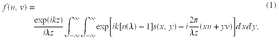
- where k=2π/λ defines the magnitude of the wavevector and n(λ) gives the index of refraction at wavelength λ. The coordinates (x,y) define a point in the plane of the screen.
- The integral over the whole surface can be broken into integrals over N cells D j, j=1, . . . , N, that completely cover the substrate surface. In its most general form, the shape of a microstructure contained in each cell is expressed as a local surface shape sj, j=1, . . . , N, where in general sp≠sq, for p≠q. The field f can now be written as
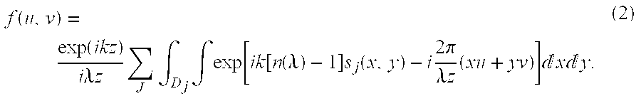
- The above expression illustrates the significant elements involved in the design of the structured screens of the invention. The first element is the shape of individual elements s j(x,y). The second is the cell Dj, where the individual element is contained. The prior art has had limited control over the elementary functions sj(x,y) except to guarantee some amount of focusing power, and the cells have usually been square or hexagonal.
- The present invention improves upon previous approaches by (i) allowing exact definition of the shape s j(x,y) to, for example, a sub-micron accuracy; (ii) allowing precise definition of the spatial localization of the domain of each cell Dj relative to any other cell; and (iii) allowing precise definition of the cell shape Dj, not limited to only square or hexagonal arrays, but assuming any contour necessary to implement the desired spreading pattern.
- B. Surface Definition
- (1) Microstructures Per Se
- The surface-relief pattern on any one side or on both sides of the structured screen is responsible for the spreading of the incident illumination. This pattern achieves the goal of shaping the diffused illumination by a specified arrangement and choice of elementary units, which are generally different from each other and are displaced at specific distances from each other, according to the requirements of the desired beam shaping.
- In a general form, the shape of each elementary unit can be defined in terms of segments characterized by piecewise functions. The general shape can assume either a continuous or discontinuous form and can also impart focusing power to the incident illumination. The particular shape of each individual element is of fundamental importance in shaping the diffused light. Thus, in accordance with the invention, the elementary shape is precisely control to tailor the diffusion profile.
- As an illustration, FIG. 2 shows diffusion patterns for of two regular arrays of identical relief depth but with the shape of each elementary unit in one array being different from the shape of each unit in the other array. In both cases the total relief depth is the same. The difference in the patterns is evident in this figure.
- A comparison between the profiles of each individual shape for the two arrays is shown in FIG. 3, while the difference between the two profiles is shown in FIG. 4. Note that to achieve the kind of diffusion control illustrated by the two curves of FIG. 2, it is necessary to ensure microstructure relief control on the order of, for example, a few microns.
- To further emphasize the importance of the shape of the elementary units, we note from grating theory that, while the grating period and wavelength determines the divergence angles of diffracted orders, the grating profile determines the distribution of power among orders. For example, a triangular blazed grating can be designed for 100% theoretical efficiency at a single order. On the other hand, custom shapes can be obtained that spread the incident illumination over many orders. Such control of the light spread is only possible with proper choice of the elementary shape of the grating.
- As discussed above, the prior art commonly relies on elementary units of spherical shape to accomplish light diffusion. The spherical shape can be expressed according to the following equation

- where c denotes the curvature of the surface and (xc,yc) is the center point. As can be seen in this equation, the only degree of freedom available to control the diffusion is the curvature or the focusing power.
- To introduce additional degrees of freedom and to allow for a wider class of surfaces, the surface shape can be written as follows:
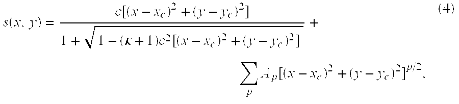
- where one finds the conic constant κ and the aspheric terms {A p} as new degrees of freedom, as compared to Eq. (3). The spherical shape is obtained in the particular case of κ=0 and Ap=0, for all p. With more degrees of freedom, it becomes possible to control the diffusion pattern better so as to satisfy specific system requirements.
- Although Eq. (4) allows a wide variety of shapes to be implemented, it is limited to conic surfaces with aspheric corrections. However, in accordance with the invention, any surface that can be defined by a mathematical relation can be implemented, including mathematical relations based on algorithmic processes. In general, the surface can be specified as a piecewise function over the boundary of the microstructure such that within each interval the surface can be expanded in a power series of the form:

- where (x c,yc) is the center point and s(x,y) is defined over a limited area of the microstructure. The total function over the complete area of the microstructure would then be defined in a piecewise manner.
- In addition to the foregoing, the present invention also allows the profile of each micro structure to vary across all or part of an array with each microstructure still being controlled to, for example, sub-micron accuracy. In this way it is possible to homogenize the diffused light and avoid the visual artifacts caused by a periodic array.
- The implementation of regular arrays has some advantages from a fabrication point of view but the performance of the screen may not be satisfactory due to the introduction of image artifacts such as high- frequency intensity variations. Furthermore, the control of light diffusion is limited because an array in general will not meet all types of system criteria. In some broadband applications, regular arrays may be acceptable because the smoothing by spectral dispersion helps to minimize the image artifacts due to the grating structure.
- The behavior of a regular array is shown in FIG. 5 for parabolic microlenses of diameter equal to 100 μm and
depth 5 μm. The incident illumination belongs to the 400-700 nm spectral band. One observes that although diffusion is accomplished, high-frequency intensity variations are present and higher-order components are noticeable. - FIG. 6 shows the diffusion obtained by a regular parabolic array of
diameter 100 μm but with depth randomly chosen in the range 5-10 μm, averaged over several statistically identical screen configurations. The intensity diffusion can be well-described by a fourth-order supergaussian with an angular spread of about 7.7 degrees measured at the 1/e2 intensity point. The randomization avoids the high-frequency structure as well as high order diffraction angles. Note that these calculations assume a spatially coherent beam incident on the aperture. In practice, partial coherence effects would further reduce the intensity fluctuations. - FIG. 7 shows another diffusion pattern of parabolic units with random depth in the range 5-10 μm and with the diameter sizes of each unit randomly chosen with a variation in the range ±20% with respect to the nominal diameter of 100 μm. The main difference with respect to the pattern of FIG. 6 is the elongated tail of Lorentzian shape.
- Control of the diffusion process depends on the particular way microstructures differ from each other. In general, this variability can be expressed in terms of a probability distribution function (PDF) for a particular parameter(s) of choice. For instance, if the array presents microlens structures with random radii of curvature, then there exists a PDF that defines how the radius of curvature varies across the array. Similarly, the PDF might refer to a conic constant, the depth of a given microstructure, the location of a given microstructure, the size of a given microstructure, any combination of these parameters, or any other relevant parameters or combinations thereof.
- In all cases, the PDF can be arbitrarily defined and an array can be accordingly built. The exact correspondence between the actual array and the PDF that describes it requires that each elementary microstructure be fabricated with, for example, sub-micron accuracy. Methods for specifying a PDF depend largely on the desired properties of the diffusion pattern but can be of either a deterministic or statistical nature.
- To illustrate the effect of the particular choice of a PDF consider a two-dimensional array of spherical microlenses with a hexagonal arrangement. Each microlens has an external circumference whose diameter is 750 μm and a total sag in the range 4-16 μm. First consider the case where the PDF is uniform in radius of curvature. For a given realization of the array, the histograms of radii and microlens sag are shown in FIGS. 8 and 9, respectively. The corresponding diffusion pattern is shown in FIG. 10.
- Now consider a random array with the same sag range but with a uniform PDF in sag instead of radius of curvature. For a given realization of the array, the histograms of radii and sag are shown in FIGS. 11 and 12, respectively. The corresponding diffusion pattern is shown in FIG. 13. The difference in the PDF for these two cases leads to fundamentally distinct arrays and the difference is reflected in the resulting diffusion, as can be readily seen by comparing FIG. 10 with FIG. 13. (2) Distribution of Microstructures
- As described above, an accurate description of the screen surface or surfaces requires two basic elements. The first element is the microstructure itself, which can be of any particular shape, as discussed immediately above. The second element is the relative spatial placement of the individual microstructures where each microstructure is spatially placed with respect to each other arbitrarily and with, for example, sub- micron accuracy. These two elements, together with the properties of the light that illuminates the screen, determine in a unique way the diffusive features of the screen. While the shape of each microstructure has a predominant effect over the functional properties of the diffusion, the spatial placement of microstructures determines the spatial symmetry, or lack thereof, of the diffusion.
- To define precisely the spatial placement of the microstructures on the surfaces of the screen, we define two basic sets of coordinate systems in relation to the screen. The global coordinate system can be located arbitrarily with respect to the screen and defines a reference frame from which each microstructure can be localized with respect to some arbitrary reference point such as the vertex, tip, or any other element of the microstructure.
- A local coordinate system is next associated with each microstructure. In the local reference frame the surface shape of the microstructure can be defined according to a function of the form s(x−X k,y−Yk), where s denotes the functional form of the microstructure, (x,y) denotes a point in the local coordinate system, and (Xk,Yk) is the position of the kth local coordinate system with respect to the global reference frame where k runs from 1 to the total number of microstructures present on the screen. A schematic illustration of the two reference frames is shown in FIG. 14, where for simplicity, the two dimensional case is shown, it being understood that the general case is three dimensional.
- In relation to the global coordinate system one may distinguish microstructure positioning along the surface of the screen or perpendicular to it. Along the surface, various realizations of this embodiment include regular periodic arrays, random arrays with the distance between neighbor microstructures varying as a function of position, microstructures with well-defined boundaries such as in a square or hexagonal array, microstructures with random boundaries where the size and shape of each microstructure varies as a function of position across the screen, or structures positioned on both surfaces of the screen.
- Examples of possible arrangements are illustrated in FIGS. 15 through 21. For cases which include a random component, such component will be defined in terms of a probability density function (PDF).
- In the direction perpendicular to the screen surface, there can be a vertical offset of each microstructure with respect to each other, also called piston. The presence of piston is relevant in the reduction of high-frequency intensity variations in the diffusion pattern (speckle), as well as in avoiding the presence of hot spots, which are isolated regions of the diffusion pattern that exhibit much higher intensity than the average of the whole pattern.
- The amount of piston used in any particular application will depend on the characteristics of the illumination on the screen but, in general, should be equivalent to a few optical wavelengths of the illumination. Also, the magnitude of the piston component for neighbor microstructures will typically vary randomly according to a PDF, unless it is desirable to introduce some bias in the diffusion pattern.
- FIG. 22 illustrates the effect of a vertical offset on a diffraction pattern for an elementary unit having a triangular shape. For a regular array having a grating period of 200 μm and a depth of 5 μm, light of wavelength 0.5 μm is focused at a diffracted order centered at the angular distance of −0.14 degrees with an angular divergence of 0.006 degrees. The corresponding diffraction pattern is shown in FIG. 22 by the dashed curve. The solid curve, on the other hand, is the result of an ensemble average over statistically identical arrays of triangular units with a maximum offset (piston) of 2 μm. The offset obeys a uniform probability distribution function.
- The diffusion attained through the introduction of the offset is more that one order of magnitude. Note however that this level of diffusion is peculiar to the blazed grating that was analyzed. In general, the degree of diffusion is shape-dependent. However, as a general rule, the offset helps in the smoothing of the diffusion pattern, since it helps eliminate artifacts due to the periodic grating structure.
- (3) Fresnel Function
- In addition to their diffusion function, the distributed microstructures of the invention can be used in combination with or, indeed, can constitute a Fresnel lens, whose purpose is to collimate an otherwise divergent beam of light.
- In the prior art, the use of a Fresnel lens is generally assumed and the general setup is as shown in FIG. 23. There has been some attempts to incorporate the Fresnel capability on one side of a substrate with the diffusive feature associated with the second surface as illustrated in FIG. 24. The screens of the present invention can be used with Fresnel lenses of the type shown in either of these figures.
- However, these approaches require several processing steps to provide the final screen with both capabilities at different surfaces. According to the present invention, a reduction in such processing steps can be achieved by incorporating both a diffusing function and a Fresnel function on one screen surface.
- As discussed above, in accordance with the invention, one is allowed precise control of each microstructure and its spatial localization in the frames of reference that define the structured screen. In addition to translations and piston as components of the spatial placement, one can also rotate individual elements. Significantly, such rotation allows one to achieve the function of a Fresnel lens.
- In particular, as illustrated in FIG. 25, the function of a Fresnel lens in a structured screen simply requires rotation of individual microstructures having focusing power. As can be seen in this figure, the individual microlenses have optical axes which are not parallel to the optical axis of the overall screen. Although not explicitly shown in this figure, the optical axis of the screen is typically the optical axis of the screen's substrate. By orienting the microstructures in this way, the diffusive and Fresnel-collimation features can not only be integrated on a single substrate but on a single surface, thereby reducing the number of processing steps required to generate the screen and allowing large volume replication in a single step.
- C. Fabrication
- The ability to produce highly reproducible and accurate screen surfaces of the type described above requires a fabrication method that allows screens to be manufactured consistently and with point-by-point accuracy. Although other techniques can be used, the most suitable method for such a task is direct laser writing where a laser beam scans a properly prepared substrate with variable intensity.
- In such a method, a substrate such as glass is covered with, for example, a low-contrast photosensitive polymer (photoresist) that is exposed and records in a latent image the exposure pattern defined by the laser beam. Typically, the photosensitive material is positive, in which case, when the substrate is developed, the exposed material is eliminated leaving a surface relief structure.
- This surface relief structure basically defines the desired screen surface or, in some cases, its complement. See commonly assigned U.S. patent application Ser. No. 60/222,032 which is being filed concurrently herewith in the names of Geoffrey B. Gretton, G. Michael Morris, and Tasso R. M. Sales, and is entitled “Microlens Arrays Having High Focusing Efficiency,” the contents of which in its entirety is incorporated herein by reference.
- The surface relief structure obtained upon development of the photoresist may not be precisely the desired structure depending on specific performance characteristics of the fabrication process. That is, the fabrication process itself can introduce features that may be undesirable in the final product and need to be accounted for in using the process. For example, since a writing laser beam has a finite size, the final surface after development represents the profile defined by the laser exposure system convolved with the shape of the laser beam used. In some instances the presence of convolution may not be detrimental to the performance of the screen but in other cases it must be avoided. Of course, the performance requirements and operating conditions dictate the fabrication tolerances and limitations.
- The surface relief profile left on the surface of the substrate can serve as a master mold that can be used to obtain a large number of replicas according to several possible techniques including casting on a UV-curable material, injection or compression molding, and reactive ion etching into a substrate.
- A particularly preferred technique for forming the structured screens of the present invention is described in commonly assigned U.S. patent application Ser. No. 09/094,340, filed Jun. 9, 1998, and entitled “Method for Making Optical Micro-Structures Which Can Have Profile Heights Exceeding 15 Microns,” which was published on Dec. 16, 1999 as PCT Patent Publication No. WO 99/64929, the contents of which in their entireties are incorporated herein by reference. Using these techniques, microstructure shape accuracy and location to within, for example, fractions of a micron can be achieved. Moreover, by using these techniques to produce durable tools, the structured screens of the present invention can be produced inexpensively and in large volumes.
- The following, non-limiting, examples illustrate the design of structured screens using the techniques discussed above. In each example, the features of the screen surface or surfaces are controlled with enough precision at each individual location so as to allow the accurate shaping (control) of the light spreading (scattering) pattern in the far field, which is the typical location for an observer. In particular, since the scattering surface is known in detail, it is possible to reliably model its optical behavior using diffraction equations and thus determine the expected performance of the screen as well as the tolerances involved in fabricating the screen.
- As discussed above, to properly tailor the scattering pattern one needs to make use of several degrees of freedom, which can be basically separated into local and global components. The screen itself is composed of micro-elements (microstructures) that act collectively to generate the desired scattering. Each microstructure can be defined by a set of parameters. These are the local components. For example, in the case of microlenses, the local parameters could be radii of curvature, conic constants, diameters, and so on. The global parameters define the laws that must be obeyed by the local parameters (such as probability distribution functions) and the spatial location of each microstructure with respect to each other.
- As also discussed above, to define the spatial arrangement and positioning of the microstructures, one can employ a conveniently placed coordinate system that defines the center of each microstructure and a global origin. Global components are defined with respect to this coordinate system. At the origin of each microstructure one can also associate a local coordinate system that provides the reference necessary to mathematically define the microstructure. It is through the use of local and global components that one can shape to a virtually unlimited degree the scattering pattern produced by the screen.
- The examples which follow illustrate the effects of various global and local parameters on the scattering pattern of a screen. In particular, Example 1 illustrates the importance of local degrees of freedom in the shape of the scattering pattern, Examples 2 and 3 deal with vertical offset and the general spatial placement of microstructures on the screen surface or surfaces, respectively, and Example 4 addresses randomization of screen parameters. Finally, Examples 5 and 6 present illustrative applications of the invention to the production of diffusing and display screens.
- Prescriptions for the structured screens of the various examples, with reference to the figures to which the prescriptions correspond, are set forth the Screen Design Table which appears at the end of the examples.
- This example illustrates the importance of the shape of each microstructure in tailoring the light spreading pattern.
- Initially we consider a regular array of identical microstructures with a shape that can be expressed as function of one or more parameters, some of which are random variables. For instance, a microstructure of spherical shape has a sag function that is given by R−(R 2−r2)½, where R denotes the radius of curvature and r denotes the radial position from the origin. According to this definition, the array consists of spherical microlenses with possibly variable radii of curvature. The size of each microstructure is identical throughout the screen surface, so that the presence of randomness is confined to a particular parameter, namely, the radii of curvature of the spherical microlenses.
- Consider initially a screen made of silicon to operate in the infrared in a wavelength range from 2 to 4 microns. FIG. 26 shows the far-field scattering profile for an array of spherical microlenses of
diameter 100 microns. The microlens sag is fixed at 10 microns. - If we now replace the spherical microlenses by another microstructure of a distinctively different shape, triangular for instance, the scattering pattern shown in FIG. 27 is found. Note that each microstructure is an isosceles triangle of
base 100 microns anddepth 10 microns, i.e., the basic dimensions are the same as for the spherical array. Since the array is more akin to a triangular grating one observes the two separated intensity peaks corresponding to the two main diffraction orders. - As a further example, consider a hyperbolic profile with radius of curvature R=120 microns and conic constant κ=−2. With these parameters the microlens sag is again 10 microns for a diameter of 100 microns. As shown in FIG. 28, although the general scattering profile is similar to that observed with spherical microlenses (see FIG. 26), one notes the increased peak intensity at the extremes of the pattern.
- The effect of microstructure shape illustrated in FIG. 26 to FIG. 28 can be even more dramatic as the numerical aperture increases.
- As a further example of the effect of microstructure shape, consider a screen in acrylic designed to operate between 400 nm and 700 nm. The screen is composed of a regular array of spherical microlenses of
diameter 50 microns. FIG. 29 and FIG. 30 illustrate the scattering profile for such an array for two microlens depths, namely, 12 microns in FIG. 29 and 20 microns in FIG. 30. As can be seen in these figures, microlens depth provides another parameter for shaping the scattering pattern of a screen. - The case of a parabolic microlens shape with 20 microns total sag (total depth) is shown in FIG. 31. The parabolic profile allows the generation of scattering profiles of considerable flatness (and, as a result, high gain) in comparison with spherical or any other profiles. In the low sag limit there is little distinction between spherical and parabolic profiles and the scattering is virtually identical. However, as the microlens sag increases the difference between these two profiles becomes no longer negligible and this reflects directly on the scattering.
- The important lesson to be learned here is that the shape of the microstructure can be used to control the shape of the scattering profile. We have presented some examples that show the variability of the scattering as a function of the shape used. It is possible to take the inverse path and define some scattering pattern of interest and, by means of optimization algorithms, calculate the sag profile that best approximates the desired scattering pattern.
- As a final note we mention that, while the above examples have been confined to regular arrays, it is generally desirable to consider random arrays to avoid effects due to the periodicity of the array. With randomization, large intensity fluctuations tend to be minimized in the scattering pattern. Furthermore, it tends to eliminate undesirable visual effects such as aliasing or moire fringes due to the superposition of two locally periodic patterns. Randomization, however, does not significantly alter the basic shape observed with the regular array. It just makes it more homogeneous and robust.
- As illustrated in Example 1, the microstructure profile basically determines the shape and the divergence span of the scattering pattern. Randomizing the profile helps reduce the high-frequency oscillations and attain a smoother pattern. Depending on the spectral band of operation, hot spots may occur that are detrimental to the performance of the screen (see, for example, FIG. 26).
- An important element useful in homogenizing the scattering pattern and providing a further parameter to help decrease the influence of hot spots is the vertical offset or piston of the microlens. Its effect is basically to displace a microlens along its axis of symmetry by a definite quantity. The net result is that the relative position of the vertex or origin of a microstructure varies as a function of its position on the screen.
- To illustrate the effect, we again consider the array used to generate FIG. 26, that is, spherical microlenses of
diameter 100 microns andsag 10 microns. Cross-sections of the screen profile without and with piston are shown in FIG. 32 and FIG. 33, respectively. The effect of the offset on the scattering pattern is shown in FIG. 34 which should be compared with the pattern of FIG. 26. The disappearance of the central hot spot is evident in FIG. 34. - As a illustration of the homogenizing effect of a vertical offset, consider the same array of spherical microlenses shown in FIG. 33, but now operating in the visible, between 400 nm and 700 nm, instead of the infrared range. The scattering patterns with and without the vertical offset are shown in FIG. 35 by the solid and dashed lines, respectively.
- The above results make clear the effect of a vertical offset in reducing hot spots and homogenizing a scattering pattern. By using this effect alone or in combination with other randomizations, one can achieve smooth scattering patterns with a minimum of visual artifacts or strong intensity fluctuations.
- A defining global parameter of great relevance to the scattering pattern is the spatial arrangement of the microstructures on the screen. The main influence of the spatial arrangement is reflected in the overall symmetry of the scattering pattern.
- For instance, the regular square array of FIG. 36 generates a three-dimensional pattern that resembles a rectangle, depending on the divergence angles introduced by the local configuration of the microlenses. The hexagonal array of FIG. 37, on the other hand, generates a scattering pattern in the form of a hexagon which can be stretched along one direction more than another depending on the divergence angles introduced by the configuration of the microlenses.
- Apart from geometrical considerations, the overall symmetry is important in many aspects, but mainly because it affects how energy is concentrated in the observation plane. For instance, for a pattern of similar spatial extension, the hexagonal arrangement of FIG. 37 concentrates more light than the square array of FIG. 36. As a result, the scattering pattern due to a hexagonal array exhibits more gain, i.e., scattering over a specified angular range, than an equivalent square array.
- In addition to gain there are also important manufacturing issues which come into play when considering the implementation of a particular spatial arrangement. For example, because of the corners, square arrays are generally deeper than hexagonal arrays and thus more difficult to manufacture.
- From the perspective of the scattering pattern, the two factors of primary relevance are the shape of the intensity profile and the divergence angle. The shape is controlled by the profile of the microstructures (sag function) while the divergence angle is controlled by the slope of the profile (first derivative of the sag function).
- Therefore, it would seem that the particular size and distribution of microstructures should not matter, as long as the individual profiles are randomized for a smooth pattern properly defined to provide the desired divergence angles. In visual systems, however, there are additional effects associated with the spatial arrangement of microstructures that are not apparent in the scattering pattern and reflect the interaction between the projected image and the sampling effect caused by the existence of discrete individual microstructures.
- A simple example of this interaction is aliasing, easily observed in pictures of high-frequency features taken with commercial digital cameras. Another effect is the appearance of color bands that arise again as a result of finite sampling and the color distribution in projected images. Independent of the screen performance in the far field, unless the scattering elements are sufficiently small, effects due to sampling may arise and need to be addressed.
- One way to eliminate these effects completely is to use a screen design that renounces a regular spatial arrangement of microstructures. This can be done by employing a screen design where microstructures are characterized by both local parameters and a spatial boundary, where the spatial boundary is the closed line that surrounds the microstructure. For example, for a square array, the boundary is a square, while for a honeycomb, the boundary is a hexagon.
- In one dimension, a regular spatial arrangement can be avoided by using cylinders of variable diameter. In two dimensions, the boundary can be, in most general form, a polygonal curve. The complete set of polygonal curves that defines the boundaries of the microstructures in the whole screen would generally (but not necessarily always) be arranged in close-packed form, as shown in FIG. 38. Another possible arrangement, that also avoids a regular spatial arrangement and is simpler to implement, employs rectangular or other shaped cells to compose a mosaic distribution of microlenses as shown in FIG. 39. A particular advantage of a mosaic, or a general polygonal boundary, is that it reduces the influence of defects caused by the tiling of two or more screen arrays to form a larger screen.
- A particularly effective way to avoid the presence of artifacts due to the periodic repetition of microstructures on a screen is to use randomization, which can be applied to either local parameters or global parameters or to both local and global parameters, as desired.
- Any set of random numbers satisfy a probability distribution function (PDF), which basically defines the probability of choosing a given value in an allowed range of parameters. Because of its simplicity, and availability in most computers, a preferred PDF is the uniform PDF. In this case, equal probability is assigned to each value in the range of the parameter. With the ability to accurately shape each individual microstructure in the screen, the particular PDF to be used in the randomization need not be confined to a few specific types but can assume an arbitrary form. Furthermore, distinct parameters can be subjected to different PDF's, depending on the desired properties for the scattering pattern.
- As a simple illustration of the effect of a particular PDF assignment, consider the case of a random array of 100-micron diameter spherical microlenses with maximum sag in the range from 5 to 15 microns and with a vertical offset equal to a randomized ±2 microns with a uniform PDF.
- The only available parameters for randomization for the microlenses themselves are then the radius of curvature and the maximum sag of each microlens. However, in addition to the specific functional shape of the PDF to be adopted, there are two distinct procedures to attain the randomization, depending on whether the PDF refers to the radius of curvature or the maximum lens sag. Since the sag is directly related to the radius of curvature the PDF's will be likewise related.
- An illustration of this effect is shown in FIG. 40 and FIG. 41. The result of changing the parameter to which the uniform PDF is applied is shown in the scattering patterns of FIG. 42, where the pattern for a uniform PDF in sag is represented by the solid line and that for a uniform PDF in radius of curvature is represented by the dashed line. As can be seen in this figure, with the uniform distribution on sag, the scattering pattern tends to spread over a larger angular range. This larger angle scattering results from an increased number of deep-sag lens units for the uniform distribution on sag.
- Depending on the specifications of the scattering it may be desirable to use other probability distribution functions besides a uniform distribution. A Gaussian distribution, for instance, allows the concentration of a parameter (e.g., sag or radius) around a given average value. There is no limitation on the types of PDF's that can be utilized, the only restrictions being imposed by the desired performance of the system. The uniform distribution tends to be the distribution of choice for most applications, mainly due to its simplicity. In many cases of interest this is sufficient to meet the system requirements. However, the option to implement an arbitrary PDF provides an important degree of freedom for tailoring the scattering pattern.
- As discussed above, in general terms, screens can be divided into two categories, i.e., diffusing screens and display screens, based on the different requirements involved in these two applications.
- Although both types of screens are intended to spread the incident illumination homogeneously over an area larger than the area it would have been spread over without the screen, display applications typically involve a number of additional requirements related to the visual interaction with an external user. A diffusing screen, on the other hand, does not necessarily need to be used visually.
- For instance, an optical detection system might require a larger, homogeneous focal spot for a given spectral band than would be provided without a screen. The absence of visual performance requirements typically makes the design of diffusing screens somewhat easier since one must concentrate only on the size and shape of the diffusing pattern. Also, the required angular spread tends to be small, which implies the use of shallow microstructures which are easier to fabricate.
- As an example, consider an input beam equal to 4 mm in the spectral range of 2 to 4 microns which is being focused at a distance equal to 10 mm. With these parameters, the full divergence angle is approximately 0.14 degrees. However, let us assume that a beam with full divergence at half-maximum of 26 degrees is required. This task can be accomplished with the microlens array shown in FIG. 43. The resulting diffraction pattern, averaged over the spectral range is shown in FIG. 44 and cross-sections of the scattering pattern are shown on FIG. 45.
- As mentioned above, screens for display applications generally present a number of challenges in addition to spreading the illumination into a specific angular range with a certain scattering profile. Here we will be concerned only with those requirements that pertain to the properties of the scattering pattern. Visual requirements, e.g., color, contrast, and various subjective variables, involve issues that cannot be easily modeled by diffraction calculations. These are better evaluated by direct observation of a test image on a screen sample.
- A first immediate distinction from diffusive screens is that display screens are confined to the visual part of the spectrum. Another main difference is that displays generally require a larger angular range, typically spanning a total of 100 degrees useful field. In addition, the angular divergence may be different in the vertical and horizontal directions.
- An example of a scattering pattern for a display screen is shown in FIG. 46. The divergence along the fast axis is 36 degrees (estimated gain 4.9) while along the slow axis it is about 17 degrees (estimated gain 16.9). This pattern was generated with the hexagonal array of anamorphic microlenses illustrated in FIG. 47.
- Another example, obtained with an anamorphic mosaic array is shown in FIG. 48, with a portion of the array itself being shown in FIG. 49. For this mosaic design, randomness was introduced for both the individual microlens elements as well as for the sizes of the rectangular boundaries (25 to 30 microns in one direction and 45 to 50 microns in the other). The divergence along the fast axis is 33 degrees (estimated gain 5.5) while that along the slow axis is about 15 degrees (estimated gain 9.6).
- Although specific embodiments of the invention have been described and illustrated, it will be apparent to those skilled in the art that modifications and variations can be made without departing from the invention's spirit and scope. The following claims are thus intended to cover the specific embodiments set forth herein as well as such modifications, variations, and equivalents.
Screen Design Tables Array type Cylindrical Spatial arrangement Close-packed Microstructure diameter 100 μm Microstructure profile Spherical Microstructure sag range 10-10 μm Total array depth range 10 μm Microstructure randomization PDF Regular array Vertical offset 0 μm Offset randomization PDF Not applicable Wavelength range 2-4 μm Array type Cylindrical Spatial arrangement Close-packed Microstructure diameter 100 μm Microstructure profile Triangular Microstructure sag range 10-10 μm Total array depth range 10 μm Microstructure randomization PDF Regular array Vertical offset 0 μm Offset randomization PDF Not applicable Wavelength range 2-4 μm Array type Cylindrical Spatial arrangement Close-packed Microstructure diameter 100 μm Microstructure profile Aspheric Microstructure sag range 10-10 μm Total array depth range 10 μm Microstructure randomization PDF Regular array Vertical offset 0 μm Offset randomization PDF Not applicable Wavelength range 2-4 μm Array type Cylindrical Spatial arrangement Close-packed Microstructure diameter 50 μm Microstructure profile Spherical Microstructure sag range 12-12 μm Total array depth range 12 μm Microstructure randomization PDF Regular array Vertical offset 0 μm Offset randomization PDF Not applicable Wavelength range 0.4-0.7 μm Array type Cylindrical Spatial arrangement Close-packed Microstructure diameter 50 μm Microstructure profile Spherical Microstructure sag range 20-20 μm Total array depth range 20 μm Microstructure randomization PDF Regular array Vertical offset 0 μm Offset randomization PDF Not applicable Wavelength range 0.4-0.7 μm Array type Cylindrical Spatial arrangement Close-packed Microstructure diameter 50 μm Microstructure profile Parabolic Microstructure sag range 20-20 μm Total array depth range 20 μm Microstructure randomization PDF Regular array Vertical offset 0 μm Offset randomization PDF Not applicable Wavelength range 0.4-0.7 μm Array type Cylindrical Spatial arrangement Close-packed Microstructure diameter 100 μm Microstructure profile Spherical Microstructure sag range 10-10 μm Total array depth range 10 μm Microstructure randomization PDF Regular array Vertical offset 0 μm Offset randomization PDF Not applicable Wavelength range 0.4-0.7 μm Array type Cylindrical Spatial arrangement Close-packed Microstructure diameter 100 μm Microstructure profile Spherical Microstructure sag range 10-10 μm Total array depth range 10 μm Microstructure randomization PDF Regular array Vertical offset ±2 μm Offset randomization PDF Uniform Wavelength range 0.4-0.7 μm Array type Cylindrical Spatial arrangement Close-packed Microstructure diameter 100 μm Microstructure profile Spherical Microstructure sag range 10-10 μm Total array depth range 10 μm Microstructure randomization PDF Regular array Vertical offset ±2 μm Offset randomization PDF Uniform Wavelength range 0.4-0.7 μm Array type Two-dimensional Spatial arrangement Square close-packed Microstructure diameter 100 μm Microstructure profile Spherical Microstructure sag range 10-10 μm Total array depth range 10 μm Microstructure randomization PDF Regular array Vertical offset 0 μm Offset randomization PDF Not applicable Wavelength range 0.4-0.7 μm Array type Two-dimensional Spatial arrangement Hexagonal Microstructure diameter 100 μm Microstructure profile Spherical Microstructure sag range 10-10 μm Total array depth range 10 μm Microstructure randomization PDF Regular array Vertical offset 0 μm Offset randomization PDF Not applicable Wavelength range 0.4-0.7 μm Array type Two-dimensional Spatial arrangement Random polygonal boundaries Microstructure diameter 50 μm (Average) Microstructure profile Spherical Microstructure sag range 2-10 μm Total array depth range 10 μm Microstructure randomization PDF Uniform Vertical offset 0 μm Offset randomization PDF Not applicable Wavelength range 0.4-0.7 μm Array type Two-dimensional Spatial arrangement Mosaic Microstructure diameter 50 μm (Average) Microstructure profile Spherical (Anamorphic) Microstructure sag range 2-10 μm Total array depth range 10 μm Microstructure randomization PDF Uniform Vertical offset 0 μm Offset randomization PDF Not applicable Wavelength range 0.4-0.7 μm Array type Two-dimensional Spatial arrangement Hexagonal Microstructure diameter 500 μm (Average) Microstructure profile Spherical (Anamorphic) Microstructure sag range 2-8 μm Total array depth range 14 μm Microstructure randomization PDF Uniform Vertical offset ±2 μm Offset randomization PDF Uniform Wavelength range 0.4-0.7 μm Array type Two-dimensional Spatial arrangement Hexagonal Microstructure diameter 50 μm (Average) Microstructure profile Spherical (Anamorphic) Microstructure sag range 2.5-4 μm (slow axis) 9-11 μm (fast axis) Total array depth range 16 μm Microstructure randomization PDF Uniform Vertical offset ±2 μm Offset randomization PDF Uniform Wavelength range 0.4-0.7 μm Array type Two-dimensional Spatial arrangement Mosaic Microstructure diameter 25-30 mm (slow axis) 45-50 mm (fast axis) Microstructure profile Spherical Microstructure sag range 1.9-3.5 μm (slow axis) 8.8-10 μm (fast axis) Total array depth range 17.4 μm Microstructure randomization PDF Uniform Vertical offset ±2 μm Offset randomization PDF Uniform Wavelength range 0.4-0.7 μm
Claims (95)


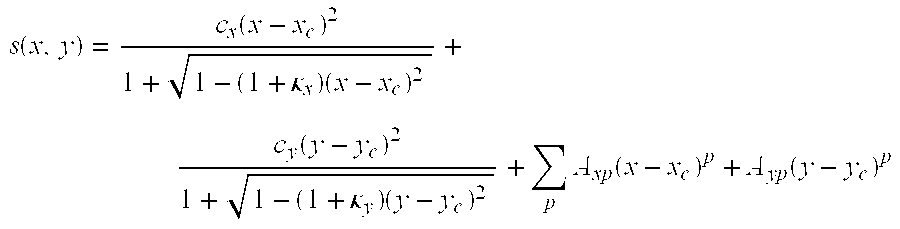
Priority Applications (1)
| Application Number | Priority Date | Filing Date | Title |
|---|---|---|---|
| US09/918,408 US7033736B2 (en) | 2000-07-31 | 2001-07-30 | Structured screens for controlled spreading of light |
Applications Claiming Priority (2)
| Application Number | Priority Date | Filing Date | Title |
|---|---|---|---|
| US22203300P | 2000-07-31 | 2000-07-31 | |
| US09/918,408 US7033736B2 (en) | 2000-07-31 | 2001-07-30 | Structured screens for controlled spreading of light |
Publications (2)
| Publication Number | Publication Date |
|---|---|
| US20020034710A1 true US20020034710A1 (en) | 2002-03-21 |
| US7033736B2 US7033736B2 (en) | 2006-04-25 |
Family
ID=22830482
Family Applications (1)
| Application Number | Title | Priority Date | Filing Date |
|---|---|---|---|
| US09/918,408 Expired - Lifetime US7033736B2 (en) | 2000-07-31 | 2001-07-30 | Structured screens for controlled spreading of light |
Country Status (8)
| Country | Link |
|---|---|
| US (1) | US7033736B2 (en) |
| EP (1) | EP1305656A4 (en) |
| JP (1) | JP2004505306A (en) |
| KR (4) | KR20020057964A (en) |
| CN (1) | CN1239925C (en) |
| AU (1) | AU2001284677A1 (en) |
| TW (1) | TWI240805B (en) |
| WO (1) | WO2002010804A1 (en) |
Cited By (76)
| Publication number | Priority date | Publication date | Assignee | Title |
|---|---|---|---|---|
| US20030002871A1 (en) * | 2001-06-20 | 2003-01-02 | Yusuke Ohmura | Microlens array, optical apparatus, single lens reflex camera and optical finder |
| US20030038999A1 (en) * | 1998-04-15 | 2003-02-27 | Knox Richard M. | Projection screen apparatus |
| EP1395052A1 (en) * | 2002-08-30 | 2004-03-03 | Seiko Epson Corporation | Light transmittive screen and rear projector |
| US6816306B2 (en) | 1998-04-15 | 2004-11-09 | Bright View Technologies Inc. | Micro-lens array based light transmitting screen with high resolution and low imaging artifacts |
| US6829087B2 (en) | 1998-04-15 | 2004-12-07 | Bright View Technologies, Inc. | Micro-lens array based light transmitting screen with tunable gain |
| US20050058947A1 (en) * | 2003-09-11 | 2005-03-17 | Rinehart Thomas A. | Systems and methods for fabricating optical microstructures using a cylindrical platform and a rastered radiation beam |
| US20050058948A1 (en) * | 2003-09-11 | 2005-03-17 | Freese Robert P. | Systems and methods for mastering microstructures through a substrate using negative photoresist and microstructure masters so produced |
| US20050058949A1 (en) * | 2003-09-11 | 2005-03-17 | Wood Robert L. | Systems and methods for fabricating microstructures by imaging a radiation sensitive layer sandwiched between outer layers, and microstructures fabricated thereby |
| EP1531346A1 (en) * | 2003-11-17 | 2005-05-18 | Olympus Corporation | Focusing screen master comprising microlenses and manufacturing method thereof comprising multistage exposure process |
| US20050146795A1 (en) * | 2000-07-31 | 2005-07-07 | Gretton Geoffrey B. | Microlens arrays having high focusing efficiency |
| US20050169008A1 (en) * | 2004-02-03 | 2005-08-04 | Ayako Okazaki | Diffuser panel and optical apparatus which uses this diffuser panel |
| EP1548353A3 (en) * | 2003-12-22 | 2005-11-16 | Schott Ag | Optical arrangement with Fresnel lens |
| US6967779B2 (en) | 1998-04-15 | 2005-11-22 | Bright View Technologies, Inc. | Micro-lens array with precisely aligned aperture mask and methods of producing same |
| US20060227569A1 (en) * | 2005-03-28 | 2006-10-12 | Nec Corporation | Light source device, display device, terminal device, and optical member |
| US20060238876A1 (en) * | 2005-04-26 | 2006-10-26 | Lars Erdmann | Optical component for beam shaping |
| US20070091444A1 (en) * | 2005-09-16 | 2007-04-26 | Samsung Electro-Mechanics Co., Ltd. | Total internal reflection micro lens array |
| EP1411732A3 (en) * | 2002-10-16 | 2007-05-30 | Eastman Kodak Company | Display systems using organic laser light sources |
| WO2007121486A2 (en) | 2006-04-18 | 2007-10-25 | Lamina Lighting, Inc. | Optical devices for controlled color mixing |
| US20080049330A1 (en) * | 2006-08-25 | 2008-02-28 | 3M Innovative Properties Company | Light directing laminate |
| EP1540409A4 (en) * | 2002-09-20 | 2008-08-06 | Corning Inc | Random microlens array for optical beam shaping and homogenization |
| US20080219303A1 (en) * | 2007-03-02 | 2008-09-11 | Lucent Technologies Inc. | Color mixing light source and color control data system |
| US20090009719A1 (en) * | 2007-06-19 | 2009-01-08 | Lucent Technologies Inc. | Compact image projector |
| DE102007056402A1 (en) * | 2007-11-23 | 2009-05-28 | Osram Gesellschaft mit beschränkter Haftung | Optical component and lighting device |
| US20090179418A1 (en) * | 2006-05-12 | 2009-07-16 | Rolic Ag | Optically effective surface relief microstructures and method of making them |
| US20090185140A1 (en) * | 2008-01-22 | 2009-07-23 | Lucent Technologies, Inc. | Multi-color light source |
| US20090184659A1 (en) * | 2008-01-22 | 2009-07-23 | Gang Chen | Time division multiplexing a DC-to-DC voltage converter |
| US20090185141A1 (en) * | 2008-01-22 | 2009-07-23 | Lucent Technologies, Inc. | Diffuser configuration for an image projector |
| US20090184976A1 (en) * | 2008-01-22 | 2009-07-23 | Alcatel-Lucent | System and Method for Color-Compensating a Video Signal Having Reduced Computational Requirements |
| US20090190210A1 (en) * | 2008-01-28 | 2009-07-30 | Real D | Polarization preserving front projection sceen |
| US20100290009A1 (en) * | 2009-05-15 | 2010-11-18 | Alcatel-Lucent Usa Inc. | Image projector employing a speckle-reducing laser source |
| EP2261721A1 (en) * | 2009-06-12 | 2010-12-15 | Ushio Denki Kabushiki Kaisha | Light irradiation device |
| US20110149389A1 (en) * | 2009-12-22 | 2011-06-23 | Reald Inc. | Polarization preserving projection screen with engineered particle and method for making same |
| US20110149390A1 (en) * | 2009-12-22 | 2011-06-23 | Joel Petersen | Polarization preserving projection screen with engineered pigment and method for making same |
| US20110169410A1 (en) * | 2010-01-12 | 2011-07-14 | Ford Global Technologies, Llc | Light emitting diode headlamp for a vehicle |
| US20110234985A1 (en) * | 2010-03-26 | 2011-09-29 | Alcatel-Lucent Usa Inc. | Despeckling laser-image-projection system |
| US20120206800A1 (en) * | 2009-12-22 | 2012-08-16 | Joel Patersen | Polarization preserving projection screen with engineered pigment and method for making same |
| US8896925B2 (en) | 2011-03-15 | 2014-11-25 | Lg Chem, Ltd. | Micro-lens array sheet and backlight unit comprising the same |
| WO2015110286A1 (en) * | 2014-01-23 | 2015-07-30 | Koninklijke Philips N.V. | Light diffuser, led lamp arrangement using the same, and manufacturing method |
| EP2916149A1 (en) * | 2014-03-07 | 2015-09-09 | Ricoh Company, Ltd. | Lens array, image display apparatus, and moving body |
| US20150293271A1 (en) * | 2012-12-28 | 2015-10-15 | Asahi Glass Company, Limited | Optical device, projector, and method of producing optical device |
| EP3088923A1 (en) * | 2015-04-28 | 2016-11-02 | Ricoh Company, Ltd. | Image display device and object apparatus |
| US20170074481A1 (en) * | 2014-05-27 | 2017-03-16 | Nalux Co., Ltd. | Microlens array and optical system including the same |
| US20170184875A1 (en) * | 2014-03-24 | 2017-06-29 | Menicon Singapore Pte Ltd. | Apparatus and methods for controlling axial growth with an ocular lens |
| WO2017125875A1 (en) | 2016-01-20 | 2017-07-27 | Pure Depth Limited | Method and system using refractive beam mapper having square element profiles to reduce moire interference in autosteroscopic display |
| EP3298440A1 (en) * | 2015-03-17 | 2018-03-28 | Valeo Comfort and Driving Assistance | Image generator, particularly for head-up display device |
| US20180106930A1 (en) * | 2015-03-12 | 2018-04-19 | Kuraray Co., Ltd. | Diffuser plate |
| US20180113240A1 (en) * | 2015-04-08 | 2018-04-26 | Kuraray Co., Ltd. | Composite diffuser plate |
| EP3203275A4 (en) * | 2014-09-30 | 2018-05-30 | Kuraray Co., Ltd. | Diffusing plate and method for producing diffusing plate |
| CN108139512A (en) * | 2015-10-02 | 2018-06-08 | 迪睿合株式会社 | Diffusion plate, display device, projection device and lighting device |
| US10007033B2 (en) | 2014-01-09 | 2018-06-26 | Seiko Epson Corporation | Microlens array, method for manufacturing microlens array, electro-optical device and electronic apparatus |
| US10107989B1 (en) | 2014-03-16 | 2018-10-23 | Navitar Industries, Llc | Optical assembly for a wide field of view point action camera with low field curvature |
| US10139599B1 (en) * | 2014-03-16 | 2018-11-27 | Navitar Industries, Llc | Optical assembly for a wide field of view camera with low TV distortion |
| US10139595B1 (en) | 2014-03-16 | 2018-11-27 | Navitar Industries, Llc | Optical assembly for a compact wide field of view digital camera with low first lens diameter to image diagonal ratio |
| US10274153B2 (en) * | 2017-07-27 | 2019-04-30 | Sl Corporation | Lamp for vehicle |
| US10317652B1 (en) | 2014-03-16 | 2019-06-11 | Navitar Industries, Llc | Optical assembly for a wide field of view point action camera with low astigmatism |
| US10386604B1 (en) | 2014-03-16 | 2019-08-20 | Navitar Industries, Llc | Compact wide field of view digital camera with stray light impact suppression |
| US10509230B2 (en) * | 2017-09-28 | 2019-12-17 | Seiko Epson Corporation | Virtual display apparatus |
| US10545313B1 (en) | 2014-03-16 | 2020-01-28 | Navitar Industries, Llc | Optical assembly for a wide field of view point action camera with a low sag aspheric lens element |
| US10545314B1 (en) | 2014-03-16 | 2020-01-28 | Navitar Industries, Llc | Optical assembly for a compact wide field of view digital camera with low lateral chromatic aberration |
| US10551633B2 (en) | 2014-09-30 | 2020-02-04 | Kuraray Co., Ltd. | Diffuser plate and method for designing diffuser plate |
| CN111103641A (en) * | 2018-10-26 | 2020-05-05 | 唯亚威通讯技术有限公司 | Optical element and system |
| US10684491B2 (en) | 2015-10-02 | 2020-06-16 | Pure Depth Limited | Method and system using refractive beam mapper having square element profiles to reduce moire interference in a display system including multiple displays |
| US10739561B1 (en) | 2014-03-16 | 2020-08-11 | Navitar Industries, Llc | Optical assembly for a compact wide field of view digital camera with high MTF |
| US10816155B2 (en) | 2016-09-23 | 2020-10-27 | Carl Zeiss Jena Gmbh | Lighting device for a vehicle |
| US10969647B2 (en) | 2015-03-11 | 2021-04-06 | E Ink Corporation | Electrophoretic particle, method of manufacturing electrophoretic particle, electrophoresis dispersion liquid, electrophoresis sheet, electrophoresis device, and electronic apparatus |
| WO2021180549A1 (en) * | 2020-03-11 | 2021-09-16 | Nil Technology Aps | Diffractive optical elements |
| WO2022090835A1 (en) * | 2020-10-27 | 2022-05-05 | 3M Innovative Properties Company | Multi-level optical diffuser with high near infrared clarity |
| EP3839584A4 (en) * | 2018-09-21 | 2022-05-18 | Dexerials Corporation | Light-diffusing plate, image display device, and lighting device |
| TWI764897B (en) * | 2016-04-27 | 2022-05-21 | 日商可樂麗股份有限公司 | Diffusion plate and projection-type projector apparatus |
| US11480717B2 (en) * | 2018-10-09 | 2022-10-25 | Dr. Johannes Heidenhain Gmbh | Grating structure for a diffractive optic |
| US11537078B2 (en) | 2016-09-23 | 2022-12-27 | Carl Zeiss Jena Gmbh | Lighting device for vehicles |
| US11726237B2 (en) | 2018-09-21 | 2023-08-15 | Dexerials Corporation | Light diffuser plate, image display device, and lighting device |
| US20230341108A1 (en) * | 2020-07-13 | 2023-10-26 | IQS Group s.r.o. | Optics for luminaires |
| US12085732B1 (en) * | 2020-12-17 | 2024-09-10 | Waymo Llc | Combined collimation and diffuser lens for flood illuminator |
| US20240360991A1 (en) * | 2021-06-28 | 2024-10-31 | Lumileds Llc | Adaptive illumination for led arrays |
| US12210171B2 (en) | 2020-12-17 | 2025-01-28 | Waymo Llc | Combined collimation and diffuser lens for flood illuminator |
Families Citing this family (61)
| Publication number | Priority date | Publication date | Assignee | Title |
|---|---|---|---|---|
| WO2002077672A2 (en) | 2001-02-07 | 2002-10-03 | Corning Incorporated | High-contrast screen with random microlens array |
| KR100870800B1 (en) | 2001-02-07 | 2008-11-27 | 코닝 인코포레이티드 | Self-Aligning Caliber Mask with High Precision Caliber |
| US6862141B2 (en) * | 2002-05-20 | 2005-03-01 | General Electric Company | Optical substrate and method of making |
| JP2005059469A (en) * | 2003-08-18 | 2005-03-10 | Fuji Photo Film Co Ltd | Anti-glaring film and its manufacturing method |
| EP1697686B1 (en) | 2003-12-22 | 2011-05-04 | Auer Lighting GmbH | Lamp with stepped lens |
| JP4882224B2 (en) * | 2004-11-26 | 2012-02-22 | ソニー株式会社 | Method for manufacturing solid-state imaging device |
| KR100872250B1 (en) * | 2005-09-14 | 2008-12-05 | 삼성전기주식회사 | Screen with relief surface for wide angle diffusion and manufacturing method thereof |
| JP4674859B2 (en) * | 2005-10-27 | 2011-04-20 | 大日本印刷株式会社 | Method for measuring shape of micro lens array |
| US7583444B1 (en) | 2005-12-21 | 2009-09-01 | 3M Innovative Properties Company | Process for making microlens arrays and masterforms |
| US7941013B2 (en) | 2006-05-18 | 2011-05-10 | 3M Innovative Properties Company | Process for making light guides with extraction structures and light guides produced thereby |
| US7918583B2 (en) * | 2006-08-16 | 2011-04-05 | Rpc Photonics, Inc. | Illumination devices |
| US7813054B2 (en) * | 2007-12-14 | 2010-10-12 | Rpc Photonics, Inc. | Optical elements with saddle shaped structures for diffusing or shaping light |
| EP2101294A1 (en) * | 2008-03-12 | 2009-09-16 | Amadeus S.A.S. | A method and system for graphically displaying data |
| IL196690A0 (en) * | 2008-05-29 | 2011-08-01 | Plasan Sasa Ltd | Interchangeable door |
| JP5509566B2 (en) * | 2008-10-01 | 2014-06-04 | 凸版印刷株式会社 | Optical component and liquid crystal display unit |
| US10038304B2 (en) | 2009-02-17 | 2018-07-31 | Trilumina Corp. | Laser arrays for variable optical properties |
| US20130223846A1 (en) | 2009-02-17 | 2013-08-29 | Trilumina Corporation | High speed free-space optical communications |
| US10244181B2 (en) | 2009-02-17 | 2019-03-26 | Trilumina Corp. | Compact multi-zone infrared laser illuminator |
| KR20120007944A (en) | 2010-07-15 | 2012-01-25 | 주식회사 엘지화학 | Optical film with improved optical performance and backlight unit including the same |
| EP2673672A1 (en) | 2011-02-11 | 2013-12-18 | OSRAM GmbH | Optical component and associated illuminating device |
| US9551914B2 (en) | 2011-03-07 | 2017-01-24 | Microsoft Technology Licensing, Llc | Illuminator with refractive optical element |
| US11095365B2 (en) | 2011-08-26 | 2021-08-17 | Lumentum Operations Llc | Wide-angle illuminator module |
| JP5850312B2 (en) * | 2011-09-30 | 2016-02-03 | 大日本印刷株式会社 | Optical sheet and image display device |
| JP5896366B2 (en) * | 2012-01-13 | 2016-03-30 | エルジー・ケム・リミテッド | Microlens array sheet and backlight unit including the same |
| US9169017B2 (en) | 2012-02-15 | 2015-10-27 | The Boeing Company | Aircraft interior lighting system using structured micro lens arrays |
| US9146016B2 (en) | 2012-03-29 | 2015-09-29 | Fraen Corporation | Tiling of multiple polygons for micro-lens array |
| EP2693252B1 (en) * | 2012-08-02 | 2016-05-18 | F. Hoffmann-La Roche AG | Array optics |
| CN102798904A (en) * | 2012-08-13 | 2012-11-28 | 嘉兴市光辰光电科技有限公司 | Microlens array |
| JP6251267B2 (en) | 2012-08-14 | 2017-12-20 | コーニンクレッカ フィリップス エヌ ヴェKoninklijke Philips N.V. | Compact laser and efficient pulse delivery for photoacoustic imaging |
| EP2708803A1 (en) | 2012-09-14 | 2014-03-19 | Thales Deutschland GmbH | Universal traffic light luminaire |
| US9209222B2 (en) | 2012-12-14 | 2015-12-08 | Hamilton Sundstrand Corporation | Surveillance device |
| US9217554B1 (en) | 2013-02-15 | 2015-12-22 | Rpc Photonics, Inc. | Optical element providing oblique illumination and apparatuses using same |
| US9239141B1 (en) | 2013-02-15 | 2016-01-19 | Rpc Photonics, Inc. | Optical element providing oblique illumination and apparatuses using same |
| CN105874662B (en) * | 2013-04-22 | 2019-02-22 | 三流明公司 | Microlenses for multi-beam arrays of optoelectronic devices operating at high frequencies |
| US9709711B1 (en) | 2013-09-18 | 2017-07-18 | Hrl Laboratories, Llc | Wavelength selective optical diffuser |
| JP2015060092A (en) * | 2013-09-19 | 2015-03-30 | ウシオ電機株式会社 | Light source device and projector |
| KR102163728B1 (en) | 2013-12-05 | 2020-10-08 | 삼성전자주식회사 | Camera for depth image measure and method of measuring depth image using the same |
| JP6260819B2 (en) * | 2014-02-20 | 2018-01-17 | カシオ計算機株式会社 | Light source device and projector |
| US9507985B2 (en) | 2014-03-31 | 2016-11-29 | Symbol Technologies, Llc | Optical lens for using in illumination system of imaging scanner |
| TWI509487B (en) * | 2014-04-25 | 2015-11-21 | Coretronic Corp | Interactive touch system and light source device |
| TWI684048B (en) | 2014-10-07 | 2020-02-01 | 美商康寧公司 | Direct view display device and light unit for direct view display device |
| JP6804830B2 (en) * | 2015-06-17 | 2020-12-23 | 株式会社クラレ | Diffusion plate |
| JP6588263B2 (en) | 2015-07-16 | 2019-10-09 | デクセリアルズ株式会社 | Diffusion plate, display device, projection device, and illumination device |
| EP3365723B1 (en) * | 2015-10-02 | 2021-12-22 | Aptiv Technologies Limited | Method and system for performing sub-pixel compression in order to reduce moiré interference in a display system including multiple displays |
| KR20180101321A (en) * | 2015-10-02 | 2018-09-12 | 푸에뎁스 리미티드 | Method and system for using a refractive beam mapper to reduce moire interference in a display system including multiple displays |
| HUE067433T2 (en) * | 2015-10-29 | 2024-10-28 | Dexerials Corp | Diffuser, method for designing diffuser, method for manufacturing diffuser, display device, projection device, and illumination device |
| JP6884518B2 (en) | 2015-10-29 | 2021-06-09 | デクセリアルズ株式会社 | Diffusing plate, diffuser plate design method, diffuser plate manufacturing method, display device, projection device and lighting device |
| US9726824B1 (en) * | 2016-09-15 | 2017-08-08 | Google Inc. | Optical circuit switch collimator |
| EP3521873B1 (en) | 2016-10-03 | 2024-09-25 | Kuraray Co., Ltd. | Diffusion plate and projection-type image display device |
| JP6826433B2 (en) * | 2016-12-28 | 2021-02-03 | デクセリアルズ株式会社 | Reflective diffuser, display device, projection device and lighting device |
| CN110678796B (en) | 2017-06-01 | 2022-05-24 | 昕诺飞控股有限公司 | Collimator device, lighting device, lamp and luminaire |
| CN111742248B (en) | 2018-02-22 | 2022-11-25 | 株式会社可乐丽 | Diffusion plate |
| US11442282B2 (en) | 2018-10-26 | 2022-09-13 | Viavi Solutions Inc. | Optical element including a plurality of regions |
| US20220128742A1 (en) | 2019-01-25 | 2022-04-28 | Kuraray Co., Ltd. | Diffuser plate |
| CN110850599A (en) * | 2019-08-19 | 2020-02-28 | 上海鲲游光电科技有限公司 | Infrared floodlighting assembly |
| US11722648B2 (en) * | 2020-07-07 | 2023-08-08 | Mirraviz, Inc. | Reflective display |
| CN116457706B (en) | 2020-11-17 | 2025-12-23 | 株式会社可乐丽 | Microarray type diffusion plate |
| KR102640340B1 (en) * | 2022-02-23 | 2024-02-23 | 인하대학교 산학협력단 | Method and Apparatus of Data Augmentation by Frequency Filtering for in X-ray Image Classification |
| CN114662291B (en) * | 2022-03-07 | 2025-02-28 | 苏州欧普照明有限公司 | A microstructure arrangement method and a diffusion plate |
| WO2023190682A1 (en) * | 2022-03-30 | 2023-10-05 | デクセリアルズ株式会社 | Diffusion plate and device |
| WO2023190680A1 (en) * | 2022-03-30 | 2023-10-05 | デクセリアルズ株式会社 | Diffuser plate, display device, projection device, and lighting device |
Citations (12)
| Publication number | Priority date | Publication date | Assignee | Title |
|---|---|---|---|---|
| US4076384A (en) * | 1975-05-02 | 1978-02-28 | Agfa-Gevaert, A.G. | Rear-projection viewing screen |
| US4531812A (en) * | 1982-03-10 | 1985-07-30 | Hitachi, Ltd. | Rear projection screen |
| US4721361A (en) * | 1986-01-28 | 1988-01-26 | U.S. Philips Corporation | Rear projection image viewing system |
| US5066099A (en) * | 1989-04-26 | 1991-11-19 | Hitachi, Ltd. | Rear projection screen and method of producing the same |
| US5177637A (en) * | 1990-09-11 | 1993-01-05 | Nikon Corporation | Focusing screen including different height microlenses arranged in a cyclical pattern |
| US5475533A (en) * | 1993-08-02 | 1995-12-12 | Applied Physics Research, L.P. | Apparatus for enhancing the brightness of an image and method of making the same |
| US6014259A (en) * | 1995-06-07 | 2000-01-11 | Wohlstadter; Jacob N. | Three dimensional imaging system |
| US6301051B1 (en) * | 2000-04-05 | 2001-10-09 | Rockwell Technologies, Llc | High fill-factor microlens array and fabrication method |
| US6317263B1 (en) * | 1999-06-18 | 2001-11-13 | 3M Innovative Properties Company | Projection screen using dispersing lens array for asymmetric viewing angle |
| US6327083B1 (en) * | 1995-04-06 | 2001-12-04 | Philips Electronics North America Corporation | Rear projection screen with reduced speckle |
| US6335828B1 (en) * | 1998-10-26 | 2002-01-01 | Kabushiki Kaisha Toshiba | Micro-lens array sheet |
| US6490086B2 (en) * | 1996-12-09 | 2002-12-03 | Canon Kabushiki Kaisha | Image display apparatus |
Family Cites Families (85)
| Publication number | Priority date | Publication date | Assignee | Title |
|---|---|---|---|---|
| US1942841A (en) | 1931-01-19 | 1934-01-09 | Shimizu Takeo | Daylight screen |
| US2338654A (en) | 1942-04-08 | 1944-01-04 | Eastman Kodak Co | Projection screen |
| US2362573A (en) | 1942-06-03 | 1944-11-14 | Eastman Kodak Co | Projection screen |
| US2358070A (en) | 1942-06-25 | 1944-09-12 | Eastman Kodak Co | Projection screen |
| US2618198A (en) | 1947-11-22 | 1952-11-18 | Eastman Kodak Co | Projection screen |
| US2984152A (en) | 1951-11-23 | 1961-05-16 | William T Snyder | Projection screens |
| US2804801A (en) | 1951-11-23 | 1957-09-03 | William T Snyder | Projection screens |
| US3063339A (en) | 1958-06-18 | 1962-11-13 | William J Snyder | Projection screens |
| US3619022A (en) | 1970-09-17 | 1971-11-09 | Ibm | Method of making an object dependent diffuser |
| DE2511390C2 (en) | 1975-03-15 | 1984-03-15 | Agfa-Gevaert Ag, 5090 Leverkusen | Method and device for the production of daylight projection screens as well as daylight projection screen produced according to this method |
| US3994562A (en) | 1975-07-18 | 1976-11-30 | Holzel Thomas M | Projection screen |
| JPS5483846A (en) | 1977-12-16 | 1979-07-04 | Canon Inc | Diffusing plate |
| US4372649A (en) | 1978-05-22 | 1983-02-08 | Minnesota Mining And Manufacturing Company | Extended area diffractive subtractive color filters |
| US4241980A (en) | 1978-05-24 | 1980-12-30 | William C. McGeehon | Beam emission control means |
| US4427265A (en) | 1980-06-27 | 1984-01-24 | Canon Kabushiki Kaisha | Diffusion plate |
| US4536056A (en) | 1981-10-05 | 1985-08-20 | Hitachi, Ltd. | Rear projection apparatus |
| US4464030A (en) | 1982-03-26 | 1984-08-07 | Rca Corporation | Dynamic accuracy X-Y positioning table for use in a high precision light-spot writing system |
| DK162413C (en) | 1982-06-10 | 1992-03-23 | Dainippon Printing Co Ltd | Rear illuminated projection screen |
| JPS60165601A (en) * | 1984-02-09 | 1985-08-28 | Nippon Gakki Seizo Kk | Holography device |
| GB2173915B (en) | 1985-03-05 | 1989-05-10 | Nippon Sheet Glass Co Ltd | Plate microlens having gradient index lenses and manufacture thereof |
| US4689291A (en) * | 1985-08-30 | 1987-08-25 | Xerox Corporation | Pedestal-type microlens fabrication process |
| DE3541327A1 (en) | 1985-11-22 | 1987-05-27 | Schwerionenforsch Gmbh | SPREADING PLATE FOR COLLECTING A REAL IMAGE IN OPTICAL SYSTEMS |
| US4668080A (en) | 1985-11-29 | 1987-05-26 | Rca Corporation | Method and apparatus for forming large area high resolution patterns |
| NL8503526A (en) | 1985-12-20 | 1987-07-16 | Philips Nv | TRANSPARENT PROJECTION SCREEN. |
| JP2503485B2 (en) | 1987-03-11 | 1996-06-05 | 株式会社ニコン | Focus plate and manufacturing method thereof |
| US4882262A (en) | 1987-09-28 | 1989-11-21 | Honeywell Inc. | Self-aligning aperture |
| EP0511721A3 (en) * | 1987-10-06 | 1992-11-25 | Koninklijke Philips Electronics N.V. | Front projection screen with reflected light concentrating lens array |
| US4767186A (en) | 1987-10-06 | 1988-08-30 | North American Philips Consumer Electronics Corp. | Front projection screen with rear light concentrating lens array |
| JP2572626B2 (en) | 1988-04-28 | 1997-01-16 | 旭光学工業株式会社 | Method of forming reticle and microstructure array |
| US4982214A (en) * | 1988-05-07 | 1991-01-01 | Canon Kabushiki Kaisha | Focusing screen |
| JPH0264501A (en) | 1988-08-30 | 1990-03-05 | Sharp Corp | Microlens array and its manufacturing method |
| DE69022504T2 (en) | 1989-07-19 | 1996-03-28 | Sharp Kk | Image display device. |
| JPH03122614A (en) | 1989-10-05 | 1991-05-24 | Matsushita Electric Ind Co Ltd | Microlens manufacturing method |
| US5148322A (en) | 1989-11-09 | 1992-09-15 | Omron Tateisi Electronics Co. | Micro aspherical lens and fabricating method therefor and optical device |
| JP2881877B2 (en) | 1989-12-21 | 1999-04-12 | 株式会社ニコン | Reticle |
| US5119235A (en) | 1989-12-21 | 1992-06-02 | Nikon Corporation | Focusing screen and method of manufacturing same |
| US5401968A (en) | 1989-12-29 | 1995-03-28 | Honeywell Inc. | Binary optical microlens detector array |
| JPH03214101A (en) | 1990-01-18 | 1991-09-19 | Nippon Sheet Glass Co Ltd | Closed packed lens array |
| US5442482A (en) * | 1990-05-21 | 1995-08-15 | Johnson; William N. H. | Microlens screens, photopolymerisable materials and artifacts utilising the same |
| JPH04119339A (en) | 1990-09-11 | 1992-04-20 | Nikon Corp | Focus plate |
| JPH04220631A (en) | 1990-12-21 | 1992-08-11 | Nikon Corp | Reticle |
| US5155631A (en) | 1990-10-01 | 1992-10-13 | The United States Of America As Represented By The Department Of Energy | Method for fabrication of cylindrical microlenses of selected shape |
| US5080706A (en) | 1990-10-01 | 1992-01-14 | The United States Of America As Represented By The Department Of Energy | Method for fabrication of cylindrical microlenses of selected shape |
| US5298366A (en) | 1990-10-09 | 1994-03-29 | Brother Kogyo Kabushiki Kaisha | Method for producing a microlens array |
| JP3067114B2 (en) | 1991-06-04 | 2000-07-17 | ソニー株式会社 | Micro lens formation method |
| CA2071598C (en) | 1991-06-21 | 1999-01-19 | Akira Eda | Optical device and method of manufacturing the same |
| JP3096098B2 (en) * | 1991-07-17 | 2000-10-10 | 株式会社リコー | Liquid crystal display |
| JPH0553174A (en) | 1991-08-27 | 1993-03-05 | Nikon Corp | Focusing screen |
| JP2581308Y2 (en) * | 1992-03-25 | 1998-09-21 | 株式会社エンプラス | Surface light source device |
| US5733710A (en) | 1991-12-03 | 1998-03-31 | Asahi Kogaku Kogyo Kabushiki Kaisha | Method for manufacturing a master die for a diffusion plate and diffusion plate manufactured by said method |
| US5245454A (en) * | 1991-12-31 | 1993-09-14 | At&T Bell Laboratories | Lcd display with microtextured back reflector and method for making same |
| JP2856612B2 (en) | 1992-10-12 | 1999-02-10 | シャープ株式会社 | Projection device for holographic stereogram recording |
| US5300263A (en) | 1992-10-28 | 1994-04-05 | Minnesota Mining And Manufacturing Company | Method of making a microlens array and mold |
| JP3191464B2 (en) | 1992-11-17 | 2001-07-23 | オムロン株式会社 | Image display device and microlens array for image display device |
| US5439621A (en) | 1993-04-12 | 1995-08-08 | Minnesota Mining And Manufacturing Company | Method of making an array of variable focal length microlenses |
| US5471327A (en) | 1993-05-14 | 1995-11-28 | Kaiser Optical Systems, Inc. | Holographic diffuser for back-lit display |
| US5695895A (en) | 1993-06-15 | 1997-12-09 | Nashua Corporation | Randomised mask for a diffusing screen |
| AU6245994A (en) | 1993-07-27 | 1995-02-28 | Physical Optics Corporation | High-brightness directional viewing screen |
| JPH08512003A (en) | 1993-07-27 | 1996-12-17 | フィジィカル オプティクス コーポレーション | Light source disassembly molding device |
| US5536455A (en) | 1994-01-03 | 1996-07-16 | Omron Corporation | Method of manufacturing lens array |
| JP3251150B2 (en) | 1994-12-29 | 2002-01-28 | 日本板硝子株式会社 | Flat microlens array and method of manufacturing the same |
| JPH08190135A (en) | 1995-01-11 | 1996-07-23 | Olympus Optical Co Ltd | Metal mold for focal plate and focal plate |
| JPH08248403A (en) | 1995-03-14 | 1996-09-27 | Kuraray Co Ltd | Liquid crystal display |
| JPH08340545A (en) | 1995-06-13 | 1996-12-24 | Matsushita Electric Ind Co Ltd | Projection type image display device |
| JPH0961631A (en) * | 1995-08-22 | 1997-03-07 | Nippon Chemitec Kk | Light guide plate and planar illuminator using the light guide plate |
| US5631754A (en) | 1995-10-20 | 1997-05-20 | Physical Optics Corporation | Holographic high contrast viewing screen embedded in a liquid crystal display |
| WO1997016765A1 (en) | 1995-11-02 | 1997-05-09 | Philips Electronics N.V. | Picture display device |
| SG63687A1 (en) | 1996-01-10 | 1999-03-30 | Sumitomo Chemical Co | A microlens-array production method thereof and liquid crystal display device using the same |
| US5718830A (en) | 1996-02-15 | 1998-02-17 | Lucent Technologies Inc. | Method for making microlenses |
| US5861990A (en) | 1996-03-08 | 1999-01-19 | Kaiser Optical Systems | Combined optical diffuser and light concentrator |
| US5808657A (en) | 1996-06-17 | 1998-09-15 | Eastman Kodak Company | Laser printer with low fill modulator array and high pixel fill at a media plane |
| US5871653A (en) * | 1996-10-30 | 1999-02-16 | Advanced Materials Engineering Research, Inc. | Methods of manufacturing micro-lens array substrates for implementation in flat panel display |
| US5867307A (en) | 1996-11-13 | 1999-02-02 | Raytheon Company | Blur film assembly for infrared optical applications |
| TW496992B (en) * | 1997-07-29 | 2002-08-01 | Alps Electric Co Ltd | Reflector having pits and projections on a surface thereof, manufacturing method for the same, and reflection type liquid crystal display device using the same |
| US6285503B1 (en) * | 1997-08-25 | 2001-09-04 | Industrial Technology Research Institute | Holographic diffuser |
| JP4243779B2 (en) * | 1997-11-14 | 2009-03-25 | 株式会社ニコン | Diffusion plate manufacturing method, diffusion plate, microlens array manufacturing method, and microlens array |
| JPH11281976A (en) * | 1998-03-30 | 1999-10-15 | Mitsubishi Electric Corp | Light guide plate, method of manufacturing the same, mold for manufacturing light guide plate, method of manufacturing the same, surface light source device, and liquid crystal display device |
| JPH11344602A (en) | 1998-03-30 | 1999-12-14 | Seiko Epson Corp | Manufacturing method of microlens substrate with black matrix, counter substrate for liquid crystal panel, liquid crystal panel and projection display device |
| US6271900B1 (en) * | 1998-03-31 | 2001-08-07 | Intel Corporation | Integrated microlens and color filter structure |
| JPH11295508A (en) * | 1998-04-06 | 1999-10-29 | Stanley Electric Co Ltd | Light reflection device and liquid crystal display device using the same |
| JPH11295766A (en) * | 1998-04-06 | 1999-10-29 | Stanley Electric Co Ltd | Guest-host type liquid crystal display |
| US6410213B1 (en) | 1998-06-09 | 2002-06-25 | Corning Incorporated | Method for making optical microstructures having profile heights exceeding fifteen microns |
| JP2000035616A (en) | 1998-07-16 | 2000-02-02 | Toshiba Corp | Screen sheet |
| JP3475797B2 (en) * | 1998-07-28 | 2003-12-08 | 松下電工株式会社 | Manufacturing method of light diffusion plate |
| US6034817A (en) | 1999-03-25 | 2000-03-07 | Mihalakis; George M. | Image projection beam transmission apparatus |
-
2001
- 2001-07-30 KR KR1020027004153A patent/KR20020057964A/en not_active Ceased
- 2001-07-30 WO PCT/US2001/023847 patent/WO2002010804A1/en not_active Ceased
- 2001-07-30 US US09/918,408 patent/US7033736B2/en not_active Expired - Lifetime
- 2001-07-30 KR KR1020097004422A patent/KR100997608B1/en not_active Expired - Lifetime
- 2001-07-30 KR KR1020087007242A patent/KR100959976B1/en not_active Expired - Fee Related
- 2001-07-30 CN CNB018022642A patent/CN1239925C/en not_active Expired - Lifetime
- 2001-07-30 EP EP01963752A patent/EP1305656A4/en not_active Ceased
- 2001-07-30 JP JP2002515479A patent/JP2004505306A/en active Pending
- 2001-07-30 KR KR1020087028852A patent/KR100948725B1/en not_active Expired - Fee Related
- 2001-07-30 AU AU2001284677A patent/AU2001284677A1/en not_active Abandoned
- 2001-07-31 TW TW090118832A patent/TWI240805B/en not_active IP Right Cessation
Patent Citations (12)
| Publication number | Priority date | Publication date | Assignee | Title |
|---|---|---|---|---|
| US4076384A (en) * | 1975-05-02 | 1978-02-28 | Agfa-Gevaert, A.G. | Rear-projection viewing screen |
| US4531812A (en) * | 1982-03-10 | 1985-07-30 | Hitachi, Ltd. | Rear projection screen |
| US4721361A (en) * | 1986-01-28 | 1988-01-26 | U.S. Philips Corporation | Rear projection image viewing system |
| US5066099A (en) * | 1989-04-26 | 1991-11-19 | Hitachi, Ltd. | Rear projection screen and method of producing the same |
| US5177637A (en) * | 1990-09-11 | 1993-01-05 | Nikon Corporation | Focusing screen including different height microlenses arranged in a cyclical pattern |
| US5475533A (en) * | 1993-08-02 | 1995-12-12 | Applied Physics Research, L.P. | Apparatus for enhancing the brightness of an image and method of making the same |
| US6327083B1 (en) * | 1995-04-06 | 2001-12-04 | Philips Electronics North America Corporation | Rear projection screen with reduced speckle |
| US6014259A (en) * | 1995-06-07 | 2000-01-11 | Wohlstadter; Jacob N. | Three dimensional imaging system |
| US6490086B2 (en) * | 1996-12-09 | 2002-12-03 | Canon Kabushiki Kaisha | Image display apparatus |
| US6335828B1 (en) * | 1998-10-26 | 2002-01-01 | Kabushiki Kaisha Toshiba | Micro-lens array sheet |
| US6317263B1 (en) * | 1999-06-18 | 2001-11-13 | 3M Innovative Properties Company | Projection screen using dispersing lens array for asymmetric viewing angle |
| US6301051B1 (en) * | 2000-04-05 | 2001-10-09 | Rockwell Technologies, Llc | High fill-factor microlens array and fabrication method |
Cited By (143)
| Publication number | Priority date | Publication date | Assignee | Title |
|---|---|---|---|---|
| US6829087B2 (en) | 1998-04-15 | 2004-12-07 | Bright View Technologies, Inc. | Micro-lens array based light transmitting screen with tunable gain |
| US20030038999A1 (en) * | 1998-04-15 | 2003-02-27 | Knox Richard M. | Projection screen apparatus |
| US6967779B2 (en) | 1998-04-15 | 2005-11-22 | Bright View Technologies, Inc. | Micro-lens array with precisely aligned aperture mask and methods of producing same |
| US6788460B2 (en) | 1998-04-15 | 2004-09-07 | Duke University | Projection screen apparatus |
| US20040188875A1 (en) * | 1998-04-15 | 2004-09-30 | Knox Richard M. | Methods of forming localized positive optical power units a substrate |
| US6816306B2 (en) | 1998-04-15 | 2004-11-09 | Bright View Technologies Inc. | Micro-lens array based light transmitting screen with high resolution and low imaging artifacts |
| US7092165B2 (en) | 2000-07-31 | 2006-08-15 | Corning Incorporated | Microlens arrays having high focusing efficiency |
| US20050146795A1 (en) * | 2000-07-31 | 2005-07-07 | Gretton Geoffrey B. | Microlens arrays having high focusing efficiency |
| US6836619B2 (en) * | 2001-06-20 | 2004-12-28 | Canon Kabushiki Kaisha | Microlens array, optical apparatus, single lens reflex camera and optical finder |
| US20030002871A1 (en) * | 2001-06-20 | 2003-01-02 | Yusuke Ohmura | Microlens array, optical apparatus, single lens reflex camera and optical finder |
| EP1395052A1 (en) * | 2002-08-30 | 2004-03-03 | Seiko Epson Corporation | Light transmittive screen and rear projector |
| EP1540409A4 (en) * | 2002-09-20 | 2008-08-06 | Corning Inc | Random microlens array for optical beam shaping and homogenization |
| EP1411732A3 (en) * | 2002-10-16 | 2007-05-30 | Eastman Kodak Company | Display systems using organic laser light sources |
| US7763417B2 (en) | 2003-09-11 | 2010-07-27 | Tredegar Newco, Inc. | Methods for fabricating optical microstructures using a cylindrical platform and a rastered radiation beam |
| US7867695B2 (en) | 2003-09-11 | 2011-01-11 | Bright View Technologies Corporation | Methods for mastering microstructures through a substrate using negative photoresist |
| US8263318B2 (en) | 2003-09-11 | 2012-09-11 | Bright View Technologies Corporation | Methods for mastering microstructures through a substrate using negative photoresist |
| US20050058949A1 (en) * | 2003-09-11 | 2005-03-17 | Wood Robert L. | Systems and methods for fabricating microstructures by imaging a radiation sensitive layer sandwiched between outer layers, and microstructures fabricated thereby |
| US20080233519A1 (en) * | 2003-09-11 | 2008-09-25 | Bright View Technologies, Inc. | Methods for fabricating optical microstructures by imaging a radiation sensitive layer sandwiched between outer layers |
| US7192692B2 (en) | 2003-09-11 | 2007-03-20 | Bright View Technologies, Inc. | Methods for fabricating microstructures by imaging a radiation sensitive layer sandwiched between outer layers |
| US7425407B1 (en) | 2003-09-11 | 2008-09-16 | Bright View Technologies, Inc. | Methods for fabricating optical microstructures by imaging a radiation sensitive layer sandwiched between outer layers |
| US20050058948A1 (en) * | 2003-09-11 | 2005-03-17 | Freese Robert P. | Systems and methods for mastering microstructures through a substrate using negative photoresist and microstructure masters so produced |
| US20050058947A1 (en) * | 2003-09-11 | 2005-03-17 | Rinehart Thomas A. | Systems and methods for fabricating optical microstructures using a cylindrical platform and a rastered radiation beam |
| US20060275714A1 (en) * | 2003-09-11 | 2006-12-07 | Bright View Technologies, Inc. | Methods for fabricating optical microstructures using a cylindrical platform and a rastered radiation beam |
| US20070003868A1 (en) * | 2003-09-11 | 2007-01-04 | Bright View Technologies, Inc. | Systems and methods for fabricating blanks for microstructure masters by imaging a radiation sensitive layer sandwiched between outer layers, and blanks for microstructure masters fabricated thereby |
| US7190387B2 (en) | 2003-09-11 | 2007-03-13 | Bright View Technologies, Inc. | Systems for fabricating optical microstructures using a cylindrical platform and a rastered radiation beam |
| US7068433B2 (en) | 2003-11-17 | 2006-06-27 | Olympus Corporation | Focusing screen master and manufacturing method thereof |
| EP1531346A1 (en) * | 2003-11-17 | 2005-05-18 | Olympus Corporation | Focusing screen master comprising microlenses and manufacturing method thereof comprising multistage exposure process |
| US20050105188A1 (en) * | 2003-11-17 | 2005-05-19 | Olympus Corporation | Focusing screen master and manufacturing method thereof |
| EP1548353A3 (en) * | 2003-12-22 | 2005-11-16 | Schott Ag | Optical arrangement with Fresnel lens |
| US20050169008A1 (en) * | 2004-02-03 | 2005-08-04 | Ayako Okazaki | Diffuser panel and optical apparatus which uses this diffuser panel |
| US7336895B2 (en) * | 2004-02-03 | 2008-02-26 | Olympus Corporation | Diffuser panel and optical apparatus which uses this diffuser panel |
| US20060227569A1 (en) * | 2005-03-28 | 2006-10-12 | Nec Corporation | Light source device, display device, terminal device, and optical member |
| US7621665B2 (en) * | 2005-03-28 | 2009-11-24 | Nec Corporation | Light source device, display device, terminal device, and optical member |
| US7443589B2 (en) | 2005-04-26 | 2008-10-28 | Carl Zeiss Sms Gmbh | Optical component for beam shaping |
| DE102005019257B4 (en) * | 2005-04-26 | 2007-10-25 | Carl Zeiss Jena Gmbh | Optics for profile shaping of radiation |
| US20060238876A1 (en) * | 2005-04-26 | 2006-10-26 | Lars Erdmann | Optical component for beam shaping |
| DE102005019257A1 (en) * | 2005-04-26 | 2006-11-16 | Carl Zeiss Jena Gmbh | Optics for profile shaping of radiation |
| US7548376B2 (en) | 2005-09-16 | 2009-06-16 | Samsung Electro-Mechanics Co., Ltd. | Total internal reflection micro lens array |
| US20070091444A1 (en) * | 2005-09-16 | 2007-04-26 | Samsung Electro-Mechanics Co., Ltd. | Total internal reflection micro lens array |
| WO2007121486A2 (en) | 2006-04-18 | 2007-10-25 | Lamina Lighting, Inc. | Optical devices for controlled color mixing |
| US8866168B2 (en) | 2006-04-18 | 2014-10-21 | Lighting Science Group Corporation | Optical devices for controlled color mixing |
| WO2007121486A3 (en) * | 2006-04-18 | 2008-07-24 | Lamina Lighting Inc | Optical devices for controlled color mixing |
| US20070268694A1 (en) * | 2006-04-18 | 2007-11-22 | Lamina Ceramics, Inc. | Optical devices for controlled color mixing |
| EP2021837B1 (en) * | 2006-05-12 | 2014-07-09 | Rolic AG | Optically effective surface relief microstructures and method of making them |
| US10350843B2 (en) | 2006-05-12 | 2019-07-16 | Rolic Ag | Optically effective surface relief microstructures and method of making them |
| US20090179418A1 (en) * | 2006-05-12 | 2009-07-16 | Rolic Ag | Optically effective surface relief microstructures and method of making them |
| US8840146B2 (en) | 2006-05-12 | 2014-09-23 | Rolic Ag | Optically effective surface relief microstructures and method of making them |
| US20080049330A1 (en) * | 2006-08-25 | 2008-02-28 | 3M Innovative Properties Company | Light directing laminate |
| US20080219303A1 (en) * | 2007-03-02 | 2008-09-11 | Lucent Technologies Inc. | Color mixing light source and color control data system |
| US7750286B2 (en) | 2007-06-19 | 2010-07-06 | Alcatel-Lucent Usa Inc. | Compact image projector having a mirror for reflecting a beam received from a polarization beam splitter back to the polarization beam splitter |
| US20090009719A1 (en) * | 2007-06-19 | 2009-01-08 | Lucent Technologies Inc. | Compact image projector |
| US8757849B2 (en) | 2007-11-23 | 2014-06-24 | Osram Gesellschaft Mit Beschrankter Haftung | Optical component and illumination device |
| DE102007056402A1 (en) * | 2007-11-23 | 2009-05-28 | Osram Gesellschaft mit beschränkter Haftung | Optical component and lighting device |
| US20110188242A1 (en) * | 2007-11-23 | 2011-08-04 | Osram Opto Semiconductors Gmbh | Optical Component and Illumination Device |
| US20090185141A1 (en) * | 2008-01-22 | 2009-07-23 | Lucent Technologies, Inc. | Diffuser configuration for an image projector |
| US20090184659A1 (en) * | 2008-01-22 | 2009-07-23 | Gang Chen | Time division multiplexing a DC-to-DC voltage converter |
| US8129669B2 (en) | 2008-01-22 | 2012-03-06 | Alcatel Lucent | System and method generating multi-color light for image display having a controller for temporally interleaving the first and second time intervals of directed first and second light beams |
| US8109638B2 (en) | 2008-01-22 | 2012-02-07 | Alcatel Lucent | Diffuser configuration for an image projector |
| US8247999B2 (en) | 2008-01-22 | 2012-08-21 | Alcatel Lucent | Time division multiplexing a DC-to-DC voltage converter |
| US20090185140A1 (en) * | 2008-01-22 | 2009-07-23 | Lucent Technologies, Inc. | Multi-color light source |
| US20090184976A1 (en) * | 2008-01-22 | 2009-07-23 | Alcatel-Lucent | System and Method for Color-Compensating a Video Signal Having Reduced Computational Requirements |
| WO2009094136A1 (en) * | 2008-01-22 | 2009-07-30 | Alcatel-Lucent Usa Inc. | Diffuser configuration for an image projector |
| US20100188746A1 (en) * | 2008-01-28 | 2010-07-29 | Real D | Polarization preserving front projection screen microstructures |
| EA029832B1 (en) * | 2008-01-28 | 2018-05-31 | Реалд Инк. | Polarization preserving front projection screen |
| US8004758B2 (en) | 2008-01-28 | 2011-08-23 | Reald Inc. | Polarization preserving front projection screen microstructures |
| US7898734B2 (en) | 2008-01-28 | 2011-03-01 | Reald Inc. | Polarization preserving front projection screen |
| US8072681B2 (en) | 2008-01-28 | 2011-12-06 | Reald Inc. | Polarization preserving front projection screen material |
| US20090297797A1 (en) * | 2008-01-28 | 2009-12-03 | Real D | Polarization preserving front projection screen material |
| WO2009097371A1 (en) * | 2008-01-28 | 2009-08-06 | Real, D. | Polarization preserving front projection screen |
| US20090190210A1 (en) * | 2008-01-28 | 2009-07-30 | Real D | Polarization preserving front projection sceen |
| US8711477B2 (en) | 2008-01-28 | 2014-04-29 | Reald Inc. | Polarization preserving front projection screen microstructures |
| US20100290009A1 (en) * | 2009-05-15 | 2010-11-18 | Alcatel-Lucent Usa Inc. | Image projector employing a speckle-reducing laser source |
| US8226241B2 (en) | 2009-05-15 | 2012-07-24 | Alcatel Lucent | Image projector employing a speckle-reducing laser source |
| US20100315814A1 (en) * | 2009-06-12 | 2010-12-16 | Ushio Denki Kabushiki Kaisha | Light irradiation device |
| EP2261721A1 (en) * | 2009-06-12 | 2010-12-15 | Ushio Denki Kabushiki Kaisha | Light irradiation device |
| US8169699B2 (en) * | 2009-12-22 | 2012-05-01 | Reald Inc. | Polarization preserving projection screen with engineered pigment and method for making same |
| US20110149389A1 (en) * | 2009-12-22 | 2011-06-23 | Reald Inc. | Polarization preserving projection screen with engineered particle and method for making same |
| US8488240B2 (en) * | 2009-12-22 | 2013-07-16 | Reald Inc. | Polarization preserving projection screen with engineered pigment and method for making same |
| US8659828B2 (en) * | 2009-12-22 | 2014-02-25 | Reald Inc. | Polarization preserving projection screen with engineered particle and method for making same |
| US20120237675A1 (en) * | 2009-12-22 | 2012-09-20 | ReaID Inc. | Polarization preserving projection screen with engineered particle and method for making same |
| US20120206800A1 (en) * | 2009-12-22 | 2012-08-16 | Joel Patersen | Polarization preserving projection screen with engineered pigment and method for making same |
| US8194315B2 (en) * | 2009-12-22 | 2012-06-05 | ReaID Inc. | Polarization preserving projection screen with engineered particle and method for making same |
| US20110149390A1 (en) * | 2009-12-22 | 2011-06-23 | Joel Petersen | Polarization preserving projection screen with engineered pigment and method for making same |
| US9110363B2 (en) | 2009-12-22 | 2015-08-18 | Reald Inc. | Polarization preserving projection screen with engineered pigment and method for making same |
| US20110169410A1 (en) * | 2010-01-12 | 2011-07-14 | Ford Global Technologies, Llc | Light emitting diode headlamp for a vehicle |
| US8314558B2 (en) | 2010-01-12 | 2012-11-20 | Ford Global Technologies, Llc | Light emitting diode headlamp for a vehicle |
| US20110234985A1 (en) * | 2010-03-26 | 2011-09-29 | Alcatel-Lucent Usa Inc. | Despeckling laser-image-projection system |
| US8896925B2 (en) | 2011-03-15 | 2014-11-25 | Lg Chem, Ltd. | Micro-lens array sheet and backlight unit comprising the same |
| US9939561B2 (en) * | 2012-12-28 | 2018-04-10 | Asahi Glass Company, Limited | Projector having diffuser |
| US20150293271A1 (en) * | 2012-12-28 | 2015-10-15 | Asahi Glass Company, Limited | Optical device, projector, and method of producing optical device |
| US10007033B2 (en) | 2014-01-09 | 2018-06-26 | Seiko Epson Corporation | Microlens array, method for manufacturing microlens array, electro-optical device and electronic apparatus |
| WO2015110286A1 (en) * | 2014-01-23 | 2015-07-30 | Koninklijke Philips N.V. | Light diffuser, led lamp arrangement using the same, and manufacturing method |
| US10222025B2 (en) | 2014-01-23 | 2019-03-05 | Philips Lighting Holding B.V. | Light diffuser, LED lamp arrangement using the same, and manufacturing method |
| EP2916149A1 (en) * | 2014-03-07 | 2015-09-09 | Ricoh Company, Ltd. | Lens array, image display apparatus, and moving body |
| US10317652B1 (en) | 2014-03-16 | 2019-06-11 | Navitar Industries, Llc | Optical assembly for a wide field of view point action camera with low astigmatism |
| US10739561B1 (en) | 2014-03-16 | 2020-08-11 | Navitar Industries, Llc | Optical assembly for a compact wide field of view digital camera with high MTF |
| US10107989B1 (en) | 2014-03-16 | 2018-10-23 | Navitar Industries, Llc | Optical assembly for a wide field of view point action camera with low field curvature |
| US10139599B1 (en) * | 2014-03-16 | 2018-11-27 | Navitar Industries, Llc | Optical assembly for a wide field of view camera with low TV distortion |
| US10139595B1 (en) | 2014-03-16 | 2018-11-27 | Navitar Industries, Llc | Optical assembly for a compact wide field of view digital camera with low first lens diameter to image diagonal ratio |
| US10386604B1 (en) | 2014-03-16 | 2019-08-20 | Navitar Industries, Llc | Compact wide field of view digital camera with stray light impact suppression |
| US10545314B1 (en) | 2014-03-16 | 2020-01-28 | Navitar Industries, Llc | Optical assembly for a compact wide field of view digital camera with low lateral chromatic aberration |
| US10545313B1 (en) | 2014-03-16 | 2020-01-28 | Navitar Industries, Llc | Optical assembly for a wide field of view point action camera with a low sag aspheric lens element |
| US10429670B2 (en) * | 2014-03-24 | 2019-10-01 | Menicon Singapore Pte Ltd. | Apparatus and methods for controlling axial growth with an ocular lens |
| US11947194B2 (en) | 2014-03-24 | 2024-04-02 | Menicon Singapore Pte Ltd. | Apparatus and methods for controlling axial growth with an ocular lens |
| US20170184875A1 (en) * | 2014-03-24 | 2017-06-29 | Menicon Singapore Pte Ltd. | Apparatus and methods for controlling axial growth with an ocular lens |
| US10443811B2 (en) * | 2014-05-27 | 2019-10-15 | Nalux Co., Ltd. | Microlens array and optical system including the same |
| US20170074481A1 (en) * | 2014-05-27 | 2017-03-16 | Nalux Co., Ltd. | Microlens array and optical system including the same |
| US10551633B2 (en) | 2014-09-30 | 2020-02-04 | Kuraray Co., Ltd. | Diffuser plate and method for designing diffuser plate |
| US11378812B2 (en) | 2014-09-30 | 2022-07-05 | Kuraray Co., Ltd. | Diffuser plate and method for designing diffuser plate |
| EP3203275A4 (en) * | 2014-09-30 | 2018-05-30 | Kuraray Co., Ltd. | Diffusing plate and method for producing diffusing plate |
| US10451778B2 (en) | 2014-09-30 | 2019-10-22 | Kuraray Co., Ltd. | Diffuser plate and method for producing diffuser plate |
| US10969647B2 (en) | 2015-03-11 | 2021-04-06 | E Ink Corporation | Electrophoretic particle, method of manufacturing electrophoretic particle, electrophoresis dispersion liquid, electrophoresis sheet, electrophoresis device, and electronic apparatus |
| TWI713502B (en) * | 2015-03-12 | 2020-12-21 | 日商可樂麗股份有限公司 | Diffuser panel |
| US20180106930A1 (en) * | 2015-03-12 | 2018-04-19 | Kuraray Co., Ltd. | Diffuser plate |
| US11231527B2 (en) * | 2015-03-12 | 2022-01-25 | Kuraray Co., Ltd. | Diffuser plate |
| EP3298440A1 (en) * | 2015-03-17 | 2018-03-28 | Valeo Comfort and Driving Assistance | Image generator, particularly for head-up display device |
| US20180113240A1 (en) * | 2015-04-08 | 2018-04-26 | Kuraray Co., Ltd. | Composite diffuser plate |
| US10877188B2 (en) * | 2015-04-08 | 2020-12-29 | Kuraray Co., Ltd. | Composite diffuser plate |
| EP3088923A1 (en) * | 2015-04-28 | 2016-11-02 | Ricoh Company, Ltd. | Image display device and object apparatus |
| CN108139512A (en) * | 2015-10-02 | 2018-06-08 | 迪睿合株式会社 | Diffusion plate, display device, projection device and lighting device |
| US10684491B2 (en) | 2015-10-02 | 2020-06-16 | Pure Depth Limited | Method and system using refractive beam mapper having square element profiles to reduce moire interference in a display system including multiple displays |
| EP3343252A4 (en) * | 2015-10-02 | 2019-06-05 | Dexerials Corporation | DIFFUSION PLATE, DISPLAY DEVICE, PROJECTION DEVICE, AND LIGHTING DEVICE |
| US10859735B2 (en) | 2015-10-02 | 2020-12-08 | Dexerials Corporation | Diffuser plate, display device, projection device, and lighting device |
| EP3405832A4 (en) * | 2016-01-20 | 2019-10-09 | Aptiv Technologies Limited | METHOD AND SYSTEM USING REFRACTIVE RADIATION IMAGING WITH SQUARE ELEMENT PROFILES TO REDUCE MOIRE INTERFERENCE IN AN AUTOSTEREOSCOPIC DISPLAY |
| WO2017125875A1 (en) | 2016-01-20 | 2017-07-27 | Pure Depth Limited | Method and system using refractive beam mapper having square element profiles to reduce moire interference in autosteroscopic display |
| TWI764897B (en) * | 2016-04-27 | 2022-05-21 | 日商可樂麗股份有限公司 | Diffusion plate and projection-type projector apparatus |
| US10816155B2 (en) | 2016-09-23 | 2020-10-27 | Carl Zeiss Jena Gmbh | Lighting device for a vehicle |
| US11537078B2 (en) | 2016-09-23 | 2022-12-27 | Carl Zeiss Jena Gmbh | Lighting device for vehicles |
| US12314006B2 (en) | 2016-09-23 | 2025-05-27 | Carl Zeiss Jena Gmbh | Lighting device for vehicles |
| US10274153B2 (en) * | 2017-07-27 | 2019-04-30 | Sl Corporation | Lamp for vehicle |
| US10509230B2 (en) * | 2017-09-28 | 2019-12-17 | Seiko Epson Corporation | Virtual display apparatus |
| EP3839584A4 (en) * | 2018-09-21 | 2022-05-18 | Dexerials Corporation | Light-diffusing plate, image display device, and lighting device |
| US11726237B2 (en) | 2018-09-21 | 2023-08-15 | Dexerials Corporation | Light diffuser plate, image display device, and lighting device |
| US11480717B2 (en) * | 2018-10-09 | 2022-10-25 | Dr. Johannes Heidenhain Gmbh | Grating structure for a diffractive optic |
| CN111103641A (en) * | 2018-10-26 | 2020-05-05 | 唯亚威通讯技术有限公司 | Optical element and system |
| WO2021180549A1 (en) * | 2020-03-11 | 2021-09-16 | Nil Technology Aps | Diffractive optical elements |
| US12372800B2 (en) | 2020-03-11 | 2025-07-29 | Nil Technology Aps | Diffractive optical elements |
| US20230341108A1 (en) * | 2020-07-13 | 2023-10-26 | IQS Group s.r.o. | Optics for luminaires |
| US12404989B2 (en) * | 2020-07-13 | 2025-09-02 | IQS Group s.r.o. | Optics for luminaires |
| WO2022090835A1 (en) * | 2020-10-27 | 2022-05-05 | 3M Innovative Properties Company | Multi-level optical diffuser with high near infrared clarity |
| US12085732B1 (en) * | 2020-12-17 | 2024-09-10 | Waymo Llc | Combined collimation and diffuser lens for flood illuminator |
| US12210171B2 (en) | 2020-12-17 | 2025-01-28 | Waymo Llc | Combined collimation and diffuser lens for flood illuminator |
| US20240360991A1 (en) * | 2021-06-28 | 2024-10-31 | Lumileds Llc | Adaptive illumination for led arrays |
Also Published As
| Publication number | Publication date |
|---|---|
| KR20090039815A (en) | 2009-04-22 |
| KR20090006216A (en) | 2009-01-14 |
| KR20080034045A (en) | 2008-04-17 |
| KR100997608B1 (en) | 2010-11-30 |
| CN1386203A (en) | 2002-12-18 |
| WO2002010804A1 (en) | 2002-02-07 |
| US7033736B2 (en) | 2006-04-25 |
| KR20020057964A (en) | 2002-07-12 |
| TWI240805B (en) | 2005-10-01 |
| EP1305656A1 (en) | 2003-05-02 |
| JP2004505306A (en) | 2004-02-19 |
| CN1239925C (en) | 2006-02-01 |
| EP1305656A4 (en) | 2006-03-08 |
| KR100948725B1 (en) | 2010-03-22 |
| AU2001284677A1 (en) | 2002-02-13 |
| KR100959976B1 (en) | 2010-05-27 |
Similar Documents
| Publication | Publication Date | Title |
|---|---|---|
| US7033736B2 (en) | Structured screens for controlled spreading of light | |
| TWI713502B (en) | Diffuser panel | |
| US6859326B2 (en) | Random microlens array for optical beam shaping and homogenization | |
| JP6778179B2 (en) | Light diffuser | |
| US7965447B2 (en) | Optical substrate and method of making | |
| TWI653471B (en) | Design method of diffusion plate and diffusion plate | |
| US7813054B2 (en) | Optical elements with saddle shaped structures for diffusing or shaping light | |
| US6317263B1 (en) | Projection screen using dispersing lens array for asymmetric viewing angle | |
| US7639425B2 (en) | Microlens sheets having multiple interspersed anamorphic microlens arrays | |
| Sales | Structured microlens arrays for beam shaping | |
| JP2004537061A (en) | High contrast screen with random microlens array | |
| CN108351437B (en) | Diffusion plate, method for designing diffusion plate, method for manufacturing diffusion plate, display device, projection device, and illumination device | |
| US20220128742A1 (en) | Diffuser plate |
Legal Events
| Date | Code | Title | Description |
|---|---|---|---|
| AS | Assignment |
Owner name: CORNING INCORPORATED, NEW YORK Free format text: ASSIGNMENT OF ASSIGNORS INTEREST;ASSIGNOR:ROCHESTER PHOTONIC CORPORATION (NOW KNOWN AS CORNING ROCHESTER PHOTONIC CORPORATION);REEL/FRAME:014560/0436 Effective date: 20030926 |
|
| STCF | Information on status: patent grant |
Free format text: PATENTED CASE |
|
| FPAY | Fee payment |
Year of fee payment: 4 |
|
| FPAY | Fee payment |
Year of fee payment: 8 |
|
| MAFP | Maintenance fee payment |
Free format text: PAYMENT OF MAINTENANCE FEE, 12TH YEAR, LARGE ENTITY (ORIGINAL EVENT CODE: M1553) Year of fee payment: 12 |