US12317509B2 - Stacked spin-orbit-torque magnetoresistive random-access memory - Google Patents
Stacked spin-orbit-torque magnetoresistive random-access memory Download PDFInfo
- Publication number
- US12317509B2 US12317509B2 US17/393,938 US202117393938A US12317509B2 US 12317509 B2 US12317509 B2 US 12317509B2 US 202117393938 A US202117393938 A US 202117393938A US 12317509 B2 US12317509 B2 US 12317509B2
- Authority
- US
- United States
- Prior art keywords
- mram
- vertical
- mram cell
- metal layer
- cell stack
- Prior art date
- Legal status (The legal status is an assumption and is not a legal conclusion. Google has not performed a legal analysis and makes no representation as to the accuracy of the status listed.)
- Active, expires
Links
Images


Classifications
-
- H—ELECTRICITY
- H10—SEMICONDUCTOR DEVICES; ELECTRIC SOLID-STATE DEVICES NOT OTHERWISE PROVIDED FOR
- H10B—ELECTRONIC MEMORY DEVICES
- H10B61/00—Magnetic memory devices, e.g. magnetoresistive RAM [MRAM] devices
- H10B61/20—Magnetic memory devices, e.g. magnetoresistive RAM [MRAM] devices comprising components having three or more electrodes, e.g. transistors
-
- H—ELECTRICITY
- H10—SEMICONDUCTOR DEVICES; ELECTRIC SOLID-STATE DEVICES NOT OTHERWISE PROVIDED FOR
- H10N—ELECTRIC SOLID-STATE DEVICES NOT OTHERWISE PROVIDED FOR
- H10N50/00—Galvanomagnetic devices
- H10N50/01—Manufacture or treatment
-
- G—PHYSICS
- G11—INFORMATION STORAGE
- G11C—STATIC STORES
- G11C11/00—Digital stores characterised by the use of particular electric or magnetic storage elements; Storage elements therefor
- G11C11/02—Digital stores characterised by the use of particular electric or magnetic storage elements; Storage elements therefor using magnetic elements
- G11C11/16—Digital stores characterised by the use of particular electric or magnetic storage elements; Storage elements therefor using magnetic elements using elements in which the storage effect is based on magnetic spin effect
- G11C11/161—Digital stores characterised by the use of particular electric or magnetic storage elements; Storage elements therefor using magnetic elements using elements in which the storage effect is based on magnetic spin effect details concerning the memory cell structure, e.g. the layers of the ferromagnetic memory cell
-
- G—PHYSICS
- G11—INFORMATION STORAGE
- G11C—STATIC STORES
- G11C11/00—Digital stores characterised by the use of particular electric or magnetic storage elements; Storage elements therefor
- G11C11/18—Digital stores characterised by the use of particular electric or magnetic storage elements; Storage elements therefor using Hall-effect devices
-
- H—ELECTRICITY
- H01—ELECTRIC ELEMENTS
- H01F—MAGNETS; INDUCTANCES; TRANSFORMERS; SELECTION OF MATERIALS FOR THEIR MAGNETIC PROPERTIES
- H01F41/00—Apparatus or processes specially adapted for manufacturing or assembling magnets, inductances or transformers; Apparatus or processes specially adapted for manufacturing materials characterised by their magnetic properties
- H01F41/14—Apparatus or processes specially adapted for manufacturing or assembling magnets, inductances or transformers; Apparatus or processes specially adapted for manufacturing materials characterised by their magnetic properties for applying magnetic films to substrates
- H01F41/30—Apparatus or processes specially adapted for manufacturing or assembling magnets, inductances or transformers; Apparatus or processes specially adapted for manufacturing materials characterised by their magnetic properties for applying magnetic films to substrates for applying nanostructures, e.g. by molecular beam epitaxy [MBE]
- H01F41/302—Apparatus or processes specially adapted for manufacturing or assembling magnets, inductances or transformers; Apparatus or processes specially adapted for manufacturing materials characterised by their magnetic properties for applying magnetic films to substrates for applying nanostructures, e.g. by molecular beam epitaxy [MBE] for applying spin-exchange-coupled multilayers, e.g. nanostructured superlattices
- H01F41/308—Apparatus or processes specially adapted for manufacturing or assembling magnets, inductances or transformers; Apparatus or processes specially adapted for manufacturing materials characterised by their magnetic properties for applying magnetic films to substrates for applying nanostructures, e.g. by molecular beam epitaxy [MBE] for applying spin-exchange-coupled multilayers, e.g. nanostructured superlattices lift-off processes, e.g. ion milling, for trimming or patterning
-
- H—ELECTRICITY
- H10—SEMICONDUCTOR DEVICES; ELECTRIC SOLID-STATE DEVICES NOT OTHERWISE PROVIDED FOR
- H10N—ELECTRIC SOLID-STATE DEVICES NOT OTHERWISE PROVIDED FOR
- H10N50/00—Galvanomagnetic devices
- H10N50/10—Magnetoresistive devices
-
- H—ELECTRICITY
- H10—SEMICONDUCTOR DEVICES; ELECTRIC SOLID-STATE DEVICES NOT OTHERWISE PROVIDED FOR
- H10N—ELECTRIC SOLID-STATE DEVICES NOT OTHERWISE PROVIDED FOR
- H10N52/00—Hall-effect devices
- H10N52/01—Manufacture or treatment
-
- H—ELECTRICITY
- H10—SEMICONDUCTOR DEVICES; ELECTRIC SOLID-STATE DEVICES NOT OTHERWISE PROVIDED FOR
- H10N—ELECTRIC SOLID-STATE DEVICES NOT OTHERWISE PROVIDED FOR
- H10N52/00—Hall-effect devices
- H10N52/101—Semiconductor Hall-effect devices
-
- H—ELECTRICITY
- H10—SEMICONDUCTOR DEVICES; ELECTRIC SOLID-STATE DEVICES NOT OTHERWISE PROVIDED FOR
- H10N—ELECTRIC SOLID-STATE DEVICES NOT OTHERWISE PROVIDED FOR
- H10N52/00—Hall-effect devices
- H10N52/80—Constructional details
-
- H—ELECTRICITY
- H10—SEMICONDUCTOR DEVICES; ELECTRIC SOLID-STATE DEVICES NOT OTHERWISE PROVIDED FOR
- H10N—ELECTRIC SOLID-STATE DEVICES NOT OTHERWISE PROVIDED FOR
- H10N59/00—Integrated devices, or assemblies of multiple devices, comprising at least one galvanomagnetic or Hall-effect element covered by groups H10N50/00 - H10N52/00
-
- G—PHYSICS
- G11—INFORMATION STORAGE
- G11C—STATIC STORES
- G11C11/00—Digital stores characterised by the use of particular electric or magnetic storage elements; Storage elements therefor
- G11C11/02—Digital stores characterised by the use of particular electric or magnetic storage elements; Storage elements therefor using magnetic elements
- G11C11/16—Digital stores characterised by the use of particular electric or magnetic storage elements; Storage elements therefor using magnetic elements using elements in which the storage effect is based on magnetic spin effect
- G11C11/165—Auxiliary circuits
- G11C11/1673—Reading or sensing circuits or methods
-
- G—PHYSICS
- G11—INFORMATION STORAGE
- G11C—STATIC STORES
- G11C11/00—Digital stores characterised by the use of particular electric or magnetic storage elements; Storage elements therefor
- G11C11/02—Digital stores characterised by the use of particular electric or magnetic storage elements; Storage elements therefor using magnetic elements
- G11C11/16—Digital stores characterised by the use of particular electric or magnetic storage elements; Storage elements therefor using magnetic elements using elements in which the storage effect is based on magnetic spin effect
- G11C11/165—Auxiliary circuits
- G11C11/1675—Writing or programming circuits or methods
-
- H—ELECTRICITY
- H01—ELECTRIC ELEMENTS
- H01F—MAGNETS; INDUCTANCES; TRANSFORMERS; SELECTION OF MATERIALS FOR THEIR MAGNETIC PROPERTIES
- H01F10/00—Thin magnetic films, e.g. of one-domain structure
- H01F10/32—Spin-exchange-coupled multilayers, e.g. nanostructured superlattices
- H01F10/324—Exchange coupling of magnetic film pairs via a very thin non-magnetic spacer, e.g. by exchange with conduction electrons of the spacer
- H01F10/3286—Spin-exchange coupled multilayers having at least one layer with perpendicular magnetic anisotropy
-
- H—ELECTRICITY
- H01—ELECTRIC ELEMENTS
- H01F—MAGNETS; INDUCTANCES; TRANSFORMERS; SELECTION OF MATERIALS FOR THEIR MAGNETIC PROPERTIES
- H01F10/00—Thin magnetic films, e.g. of one-domain structure
- H01F10/32—Spin-exchange-coupled multilayers, e.g. nanostructured superlattices
- H01F10/324—Exchange coupling of magnetic film pairs via a very thin non-magnetic spacer, e.g. by exchange with conduction electrons of the spacer
- H01F10/329—Spin-exchange coupled multilayers wherein the magnetisation of the free layer is switched by a spin-polarised current, e.g. spin torque effect
Definitions
- the disclosure relates generally to stacked magnetoresistive random-access memory (MRAM).
- MRAM magnetoresistive random-access memory
- the disclosure relates particularly to stacked spin-orbit torque MRAM structures including a shared low resistivity spin-Hall-effect (SHE) rail.
- SHE spin-Hall-effect
- MRAM is a type of solid state, non-volatile memory that uses tunneling magnetoresistance (TMR) to store information.
- MRAM is made up of an electrically connected array of magnetoresistive memory elements, referred to as magnetic tunnel junctions (MTJs).
- Each MTJ includes a free layer and fixed layer that each include a layer of a magnetic material, and that are separated by a non-magnetic insulating tunnel barrier.
- the free layer has a variable magnetization direction
- the fixed layer has an invariable magnetization direction.
- An MTJ stores information by switching the magnetization state of the free layer. When the magnetization direction of the free layer is parallel to the magnetization direction of the fixed layer, (the P state) the MTJ is in a low resistance state.
- the MTJ when the magnetization direction of the free layer is antiparallel to the magnetization direction of the fixed layer, (the AP state) the MTJ is in a high resistance state.
- the difference in resistance of the MTJ may be used to indicate a logical ‘1’ or ‘0’, thereby storing a bit of information.
- the TMR of an MTJ determines the difference in resistance between the high and low resistance states.
- a relatively high difference between the high and low resistance states facilitates read operations in the MRAM.
- MRAM cells can be formed as a vertical stack enabling device design options for increasing device memory cell element density while maintaining or even reducing the scale of devices.
- SOT MRAM cells include a spin-orbit torque, or spin-Hall-effect (SHE), layer in contact with the magnetic tunnel junction (MTJ) structure of the MRAM.
- the SHE is typically a heavy conductive metal, such as platinum or tantalum.
- Current is passed through the SHE layer, but not through the MTJ structure, to write to the cell and current is passed through the MTJ to read the cell. Since high voltage write energies are not passed though the MTJ of the MRAM cell, SOT-MRAM tend to be more reliable and have a longer lifecycle. Less energy is used in writing the SOT-MRAM, as the write energy does not pass through the MTJ.
- SOT-MRAM densities may be increased by integrating multiple SOT-MRAM cells on a common SHE layer, sharing the SOT-MRAM driving transistors across multiple cells.
- a spin-orbit torque magnetoresistive random-access memory device formed by fabricating a plurality of stacks of vertical magnetoresistive random-access memory (MRAM) cell stacks, each stack formed upon a different bottom electrode, each stack including: a first vertical MRAM cell stack, the first vertical MRAM cell stack disposed upon a first bottom electrode, a first metal layer disposed above and in electrical contact with the first MRAM cell stack, and a second vertical MRAM cell stack, the second MRAM cell stack disposed above and in electrical contact with the first metal layer. Further by fabricating a low resistivity layer between adjacent stacks of vertical MRAM cell stacks, the low resistivity layer in electrical contact with the spin-Hall-Effect layer of each of the adjacent stacks.
- MRAM vertical magnetoresistive random-access memory
- a spin-orbit torque magnetoresistive random-access memory device includes a first vertical MRAM stack disposed upon a bottom electrode, a spin-Hall-effect (SHE) rail disposed above and in electrical contact with the first MRAM stack, and a second vertical MRAM stack disposed above and in electrical contact with the SHE rail.
- the SHE rail includes a first SHE material disposed between the first vertical MRAM stack and the second MRAM stack, and a second material disposed between and in electrical contact with the SHE material of adjacent stacks of vertical MRAM stacks.
- a spin-orbit torque magnetoresistive random-access memory device includes a plurality of first vertical MRAM stacks, each stack disposed upon a different bottom electrode, the bottom electrode in electrical communication with a semiconductor device transistor, a spin-Hall-effect (SHE) rail disposed above and in electrical contact with the first MRAM stack, and a second vertical MRAM stack disposed above and in electrical contact with the SHE rail.
- the SHE rail includes a first SHE material disposed between the first vertical MRAM stack and the second MRAM stack, and a second material disposed between and in electrical contact with the SHE material of adjacent stacks of vertical MRAM stacks.
- FIG. 1 provides a cross-sectional view of a step in the fabrication of a semiconductor device, according to an embodiment of the invention.
- the figure illustrates a stack of MRAM layers deposited upon an underlying semiconductor device.
- FIG. 2 provides a cross-sectional view of a step in the fabrication of a semiconductor device, according to an embodiment of the invention.
- the figure illustrates a plurality of MRAM cell stacks etched from the MRAM layers.
- FIG. 3 provides a cross-sectional view of a step in the fabrication of a semiconductor device, according to an embodiment of the invention.
- the figure illustrates the encapsulation of the MRAM cell stacks with a set of first protective dielectric material sidewall spacers.
- FIG. 4 provides a cross-sectional view, of a step in the fabrication of a semiconductor device, according to an embodiment of the invention.
- the figure illustrates the device after the addition of an interlayer dielectric (ILD) material layer.
- ILD interlayer dielectric
- FIG. 5 provides a cross-sectional view of a step in the fabrication of a semiconductor device, according to an embodiment of the invention. The figure illustrates the device after the addition of a second dielectric sidewall spacer.
- FIG. 6 provides a cross-sectional view of a step in the fabrication of a semiconductor device, according to an embodiment of the invention. The figure illustrates the device after the removal of portions of the second dielectric sidewall spacers.
- FIG. 7 provides a cross-sectional view of a step in the fabrication of a semiconductor device, according to an embodiment of the invention.
- the figure illustrates the device after the masking and selective etching of the first dielectric sidewall spacers, exposing spin-Hall-Effect (SHE) layers 145 of the MRAM cell stacks.
- SHE spin-Hall-Effect
- FIG. 8 provides a cross-sectional view of a step in the fabrication of a semiconductor device, according to an embodiment of the invention.
- the figure illustrates the device after the removal of the remaining portions of the second dielectric sidewalls and deposition of low resistivity material between adjacent MRAM cell stacks.
- the low resistivity material is electrically connected to the SHE material layers of the adjacent MRAM cell stacks.
- the deposition of the conductive material forms a common SHE rail between the MRAM cell stacks
- FIG. 9 provides a cross-sectional view of a step in the fabrication of a semiconductor device, according to an embodiment of the invention. The figure illustrates the device after the addition of an interlayer dielectric material and the addition of an upper metal contact for each MRAM cell stack.
- FIG. 10 provides a cross-sectional view of a step in the fabrication of a semiconductor device, according to an embodiment of the invention.
- each MRAM cell stack includes multiple sets of MRAM cells separated by common SHE rails.
- the figure illustrates the device after the addition of an interlayer dielectric material and the addition of an upper metal contact for each MRAM cell stack.
- FIG. 11 provides a flowchart depicting operational steps for forming semiconductor device, according to an embodiment of the invention.
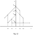
- FIG. 12 depicts a relationship between applied SHE rail write voltages and overall stacked SOT-MRAM cell device resistance, according to an embodiment of the invention.
- the present embodiments can include a design for an integrated circuit chip, which can be created in a graphical computer programming language and stored in a computer storage medium (such as a disk, tape, physical hard drive, or virtual hard drive such as in a storage access network). If the designer does not fabricate chips or the photolithographic masks used to fabricate chips, the designer can transmit the resulting design by physical means (e.g., by providing a copy of the storage medium storing the design) or electronically (e.g., through the Internet) to such entities, directly or indirectly.
- the stored design is then converted into the appropriate format (e.g., GDSII) for the fabrication of photolithographic masks, which typically include multiple copies of the chip design in question that are to be formed on a wafer.
- the photolithographic masks are utilized to define areas of the wafer (and/or the layers thereon) to be etched or otherwise processed.
- the resulting integrated circuit chips can be distributed by the fabricator in raw wafer form (that is, as a single wafer that has multiple unpackaged chips), as a bare die, or in a packaged form.
- the chip is mounted in a single chip package (such as a plastic carrier, with leads that are affixed to a motherboard or other higher-level carrier) or in a multichip package (such as a ceramic carrier that has either or both surface interconnections or buried interconnections).
- the chip is then integrated with other chips, discrete circuit elements, and/or other signal processing devices as part of either (a) an intermediate product, such as a motherboard, or (b) an end product.
- the end product can be any product that includes integrated circuit chips, ranging from toys and other low-end applications to advanced computer products having a display, a keyboard or other input device, and a central processor.
- material compounds will be described in terms of listed elements, e.g., SiGe. These compounds include different proportions of the elements within the compound, e.g., SiGe includes SixGe1-x where x is less than or equal to 1, etc.
- other elements can be included in the compound and still function in accordance with the present principles.
- the compounds with additional elements will be referred to herein as alloys.
- any of the following “/”, “and/or”, and “at least one of”, for example, in the cases of “A/B”, “A and/or B” and “at least one of A and B”, is intended to encompass the selection of the first listed option (A) only, or the selection of the second listed option (B) only, or the selection of both options (A and B).
- such phrasing is intended to encompass the selection of the first listed option (A) only, or the selection of the second listed option (B) only, or the selection of the third listed option (C) only, or the selection of the first and the second listed options (A and B) only, or the selection of the first and third listed options (A and C) only, or the selection of the second and third listed options (B and C) only, or the selection of all three options (A and B and C).
- This can be extended, as readily apparent by one of ordinary skill in this and related arts, for as many items listed.
- spatially relative terms such as “beneath,” “below,” “lower,” “above,” “upper,” and the like, can be used herein for ease of description to describe one element's or feature's relationship to another element(s) or feature(s) as illustrated in the FIGS. It will be understood that the spatially relative terms are intended to encompass different orientations of the device in use or operation in addition to the orientation depicted in the FIGS. For example, if the device in the FIGS. is turned over, elements described as “below” or “beneath” other elements or features would then be oriented “above” the other elements or features. Thus, the term “below” can encompass both an orientation of above and below.
- the device can be otherwise oriented (rotated 90 degrees or at other orientations and the spatially relative descriptors used herein can be interpreted accordingly.
- a layer when referred to as being “between” two layers, it can be the only layer between the two layers, or one or more intervening layers cat also be present.
- STT Spin-transfer torque
- MRAM magnetoresistive random-access memory
- SOT Spin-orbit torque
- SHE spin Hall-effect
- SHE Write lines need to be formed using heavy metal (W, Pt, AuW, etc.) exhibiting strong spin-orbit interaction and Spin-Hall-Effect properties for the SOT-MRAM to be functional. These metals have higher resistivity than standard middle-of-line, back-end-of-line metals such as Cu. This can lead to a significant increase of the overall SHE write line resistivity and an increase of the average power consumption/unit cell. This can also lead to a degradation of the Bitcell TMR (tunnel magnetoresistance or Read margin) by adding a more significant parasitic resistance in series with the intrinsic MTJ TMR.
- Ion beam etching (IBE) during the formation of the SOT-MRAM stack can cause back sputtering of material from a lower SOT layer, damaging the final MRAM stack and reducing the reliability of the device.
- Stacking SOT-MRAM cells to increase device cell density offer additional opportunities for detrimental back sputtering to occur during fabrication of the stacked SOT-MRAM cell elements.
- the disclosed inventions include devices and methods to fabricate stacked MRAM cell elements having a common SHE rail without detrimental back sputtering through the late formation of the common SHE rail between MRAM cell stacks.
- Such methods provide higher device densities as the MRAM cell elements share a common footprint, reducing the cost per unit of storage, simplify circuit design by sharing a SHE write line for upper and lower SOT-MRAM cells, and enable use of the SOT-MRAM cells in Neural Network applications as artificial synapse to store node weight using multiple resistance weights.
- multiple stacks are etched from material layers deposited upon an underlying semiconductor device.
- device 100 includes a succession of layers, 130 - 165 , deposited upon the dielectric material 120 and multiple bottom electrodes 125 .
- Dielectric material 120 is deposited and bottom electrodes 125 are formed upon underlying semiconductor device including dielectric material 110 and underlying device transistor contacts 115 .
- the deposited layers are etched to form the vertical magnetic—tunnel junction (MTJ) stacks of the pairs SOT-MRAM cells.
- MTJ vertical magnetic—tunnel junction
- the layers of the stacks include simplistically depicted layers for upper/lower pairs of MTJ.
- the lower MTJ including a lower reference magnetic layer 130 (a layer having a fixed magnetic dipole moment), a lower tunnel barrier layer 135 , and a lower free magnetic layer 140 (a layer having a switchable magnetic dipole moment).
- the upper MTJ includes an upper free magnetic layer 150 (a layer having a switchable magnetic dipole moment), an upper tunnel barrier layer 155 , and an upper reference magnetic layer 160 (a layer having a fixed magnetic dipole moment).
- the lower reference layer 130 may include, for example one or more interfacial layers, or spacers, and ruthenium, cobalt, palladium, tantalum, iron, boron, cobalt-platinum (Co
- reference layer 130 is between about 3 nm and about 10 nm in thickness.
- the lower tunnel barrier layers 135 is formed.
- Lower tunnel barrier layer 135 may include a non-magnetic insulating material such as magnesium oxide (MgO).
- MgO magnesium oxide
- lower tunnel barrier layer 135 is between about 1 nm and about 3 nm in thickness.
- the free layer 140 is formed on top of the lower tunnel barrier layer 135 .
- the lower MTJ includes a seed layer (not shown) having free layer 140 grown thereon.
- the seed layer may include, for example, tantalum (Ta) or tantalum magnesium (TaMg) in some embodiments.
- the free layer 140 may include cobalt-iron-boron (CoFeB), for example.
- the respective layers may be formed by PVD.
- the free layer 140 and the reference layer 130 have perpendicular magnetic anisotropy.
- the layers of the lower and upper MRAM cell stacks are separated by an SHE layer 145 deposited upon lower free layer 140 .
- SHE layer 145 consists of a heavy, conductive metal such as platinum, palladium, tungsten, cobalt, tantalum, or similar conductive metals.
- the SHE layer 145 has a thickness of between about 10 nm and about 50 nm.
- SHE layer 145 consists of Bi 2 Se 3 .
- Deposition of the SHE layer 145 occurs by deposition processes including, e.g., chemical vapor deposition (CVD), physical vapor deposition (PVD), atomic layer deposition (ALD), or similar processes.
- CVD chemical vapor deposition
- PVD physical vapor deposition
- ALD atomic layer deposition
- the upper SOT-MRAM cell stack layers deposited above the SHE layer 145 include an upper free magnetic layer 150 (a layer having a switchable magnetic dipole moment), an upper tunnel barrier layer 155 , an upper fixed magnetic layer 160 (a layer having a fixed magnetic dipole moment) and an upper contact electrode layer 165 .
- the upper SOT-MRAM cell stack layers includes a seed layer (not shown) having free magnetic layer 150 grown thereon.
- the seed layer may include, for example, tantalum (Ta) or tantalum magnesium (TaMg) in some embodiments.
- the upper free magnetic layer 150 may include cobalt-iron-boron (CoFeB), for example.
- the upper tunnel barrier layer 155 is formed on the upper free magnetic layer 150 .
- the upper tunnel barrier layer 155 may include a non-magnetic insulating material such as magnesium oxide (MgO). Following the formation of the upper tunnel barrier layer 155 , an upper fixed layer 160 is formed on top of the upper tunnel barrier layer 155 .
- the upper fixed layer 160 may include, for example, one or more interfacial layers, or spacers, and cobalt-platinum (Co
- the upper contact electrode layer 165 includes a conductive material such as a metal. The respective layers may be formed by radio-frequency sputtering.
- the upper free magnetic layer 155 and the upper fixed layer 160 have perpendicular magnetic anisotropy.
- the SOT-MRAM cell stacks including the lower MRAM stack, SHE layer, and upper MRAM stack are formed using a patterning and etching process such as reactive ion etching (RIE) or Ion Beam Etching (IBE) or a combination of both.
- RIE reactive ion etching
- IBE Ion Beam Etching
- layers 120 , and 130 - 165 have been selectively etched away using ion-beam etching, leaving the upper and lower SOT-MRAM cell stacks, separated by SHE layer 145 having a bottom electrode 135 in electrical contact with a contact 115 of a device element (e.g., a transistor) of the underlying semiconductor device.
- a device element e.g., a transistor
- the lower SOT-MRAM cell stack free layer 140 has a first thickness and a first volume.
- the upper SOT-MRAM cell stack free layer 150 has a second thickness and second volume which differ from those of the lower SOT-MRAM cell stack free layer 140 .
- the energy barrier associated with writing to each of the lower and upper SOT-MRAM cell stacks is directly related to the geometry and volume of the respective free layers.
- the relative energy barriers to writing each of the upper and lower SOT-MRAM cells are directly proportional to the volume of the free layer of each SOT-MRAM cell, as well as the magnetic anisotropy field of the material of each layer and the magnetization of saturation of the each layer.
- the anisotropy field and magnetization of saturation of each layer relate to the volume of the layers as well as the respective material types of each layer.
- the energy barrier of the free layer of the upper MRAM cell exceeds the energy barrier of the lower MRAM cell by design as the thickness and the volume of the free layer of the upper MRAM cell stack exceed the thickness and the volume of the lower MRAM cell stack.
- the upper SOT-MRAM cell has a higher energy barrier to writing than the lower SOT-MRAM cell.
- the lower SOT-MRAM cell may be written independently of the upper SOT-MRAM cell.
- the upper and lower free layer thicknesses are adjusted to tailor the respective energy barriers of the upper and lower SOT-MRAM cells.
- FIG. 3 provides a cross-sectional view of the device 100 at an intermediate stage of fabrication.
- the figure illustrates the device 100 after the addition of protective sidewalls 310 to the vertical surfaces of the MRAM cell structures.
- Exemplary protective sidewall 310 materials include SiN, SiCO, SiC, SiO 2 , and similar materials.
- sidewalls 310 are formed by conformal deposition of dielectric material, followed by anisotropic RIE of the material. Sidewall 310 materials deposited upon horizontal surfaces may be removed using anisotropic etching processes.
- an interlayer dielectric (ILD) material 410 is deposited and polished using chemical-mechanical planarization (CMP) processes.
- FIG. 4 illustrates the device after the deposition of the ILD 410 and the polishing by CMP processes.
- the upper surface of ILD layer 410 coincides with a level between the lower and upper surfaces of SHE layer 145 .
- the ILD material deposition ends above the SOT-MRAM stacks.
- the CMP processes removes ILD material to a level flush with the top of the stacks, the ILD material is then selectively removed to recess the ILD layer to a point at or near the upper surface of the SHE layers of the stacks.
- FIG. 5 illustrates the device at an intermediate fabrication stage and after the fabrication of second dielectric sidewall spacers 510 .
- Second sidewall spacers 510 are formed by the conformal deposition and selective removal of a dielectric material leaving dielectric material 510 upon the vertical surfaces of the first sidewalls 310 . In an embodiment, removal of excess material occurs using anisotropic RIE methods.
- FIG. 6 illustrates the device at an intermediate fabrication stage and after the selective removal of portions of ILD material 410 , thereby exposing portions of dielectric sidewalls 310 .
- ILD material 410 portions may be removed using anisotropic etching or other known methods. The removal of portions of the ILD 410 , exposes portions of sidewalls 310 corresponding to regions between the lower and upper surfaces of SHE layers 145 .
- FIG. 7 illustrates device 100 at an intermediate fabrication stage and after the selective removal of portions of dielectric sidewalls 310 , thereby exposing portions of SHE layers 145 .
- Dielectric sidewall 310 portions may be removed using isotropic etching or other known methods. The removal of portions of sidewalls 310 exposes vertical portions of SHE layers 145 corresponding to regions between the lower and upper surfaces of SHE layers 145 .
- FIG. 8 illustrates device 100 at an intermediate stage of fabrication. As shown in the Figure, the remaining portions of secondary dielectric sidewalls 510 have been selectively removed by etching, and secondary SHE layer material 810 has been deposited between adjacent SOT-MRAM cell stacks, connecting adjacent SOT-MRAM cell stack SHE layers 145 .
- Secondary SHE layer material 810 need not exhibit SHE properties as this portion of the SHE rail is not disposed adjacent to the free layers of the vertical MRAM cell stacks.
- Exemplary materials for secondary SHE layer material 810 include Cu, Ru, Co, and other similarly low resistivity metallic elements and alloys. Deposition, recessing, masking, and selective removal of the secondary SHE layer material 810 may be followed by appropriate CMP processes.
- FIG. 9 illustrates device 100 following final process fabrication stages to deposit and polish an upper ILD layer 910 upon the secondary SHE layer material 810 .
- contact vias are etched through ILD 910 , exposing a surface of the upper contact electrode layers 165 .
- the contact vias are then filled with a conductive metal 920 , using any of the deposition method described herein.
- conductive metal 920 includes any of Cu, Ru, Co, W, Ti, TiN, deposited using CVD, PVD, or plating processes.
- the conductive metal layer has a thickness of between about 30 nm and about 70 nm.
- RIE processes may be used to create the contact vias.
- CMP processes are then applied to create a polished upper surface for the back-end-of-line processes needed to complete and package the final semiconductor device.
- FIG. 10 illustrates an embodiment of device 100 wherein each SOT-MRAM cell stack includes multiple combinations of upper and lower SOT-MRAM cells separated by SHE rails formed of SHE layers 145 and secondary SHE materials 810 .
- Each pair of lower and upper SOT-MRAM cell stacks includes SHE write rails separating the lower and upper SOT-MRAM cells of the pair.
- the lower-upper SOT-MRAM cells—SHE rail combinations of each stack of multiple combinations are separated by a low resistivity metallic spacing layer 1010 deposited during the deposition of the multiple layers of final stack configuration, prior to etching of the individual stacks.
- SHE rails for rows of adjacent SOT-MRAM cell pairs are formed through iterations of the steps associated with FIGS. 4 - 8 , for each successive layer of SOT-MRAM cells of the stacks of cells.
- FIG. 11 provides a flowchart depicting operational steps associated with the fabrication of the disclosed SOT-MRAM devices.
- a series of layers are formed upon an underlying semiconductor device.
- the underlying semiconductor device includes a set of bottom electrodes in contact with transistors intended for the control of SOT-MRAM devices.
- the series of layers includes a lower reference layer, a lower tunnel junction layer, a lower free layer, an SHE layer, an upper free layer, and upper tunnel junction layer, an upper reference layer and an upper electrode layer. Each layer is formed across the entire cross section of the device.
- the series of layers is masked and selectively etched back leaving the SOT-MRAM cell stacks, each stack in electrical contact with a lower electrode.
- the final lower SOT-MRAM stacks are disposed above and in electrical contact with a metal contact of a read transistor of the underlying semiconductor device by way of the lower electrode.
- the etching yields an array of multiple SOT-MRAM cell stacks.
- Each stack including at least a pair of SOT-MRAM cells separated by an SHE layer.
- the SHE layer comprises a high-density conductive material having good spin-Hall-Effect properties capable of altering the spin of materials in adjacent free layers of the upper and lower SOT-MRAM cell stacks.
- the formed SOT-MRAM cell stacks are then encapsulated by a first dielectric material protective sidewall.
- the first dielectric material protective sidewall is etched back exposing the upper surface of the upper electrode layer of the SOT-MRAM cell stacks and the horizontal surface of the lower ILD material of the device.
- an interlayer dielectric material is deposited over the device and a CMP process polishes the upper surface of the ILD material.
- the upper surface of the ILD layer corresponds to a level between the lower and upper surfaces of the SHE layers of the SOT-MRAM cell stacks.
- the SHE layers of the SOT-MRAM cell stacks are exposed.
- a second dielectric sidewall is deposited above the ILD layer and in contact with the first dielectric sidewall.
- sidewall-image transfer processes or a combination of deposition and etching processes are used to form the second dielectric sidewalls.
- the ILD layer is selectively etched to a height at or above the lower surface of the SHE layers of the vertical MRAM cell stacks. exposing portions of the first dielectric sidewalls corresponding to the SHE layers of the SOT-MRAM cell stacks.
- the exposed portions of the first dielectric sidewalls are then selectively etched, exposing portions of the SHE layers of the SOT-MRAM cell stacks.
- the exposed portions of the SHE layers of adjacent stacked SOT-MRAM cells are electrically connected by the deposition of a conductive secondary SHE layer material, forming SHE write rails connecting rows of adjacent SOT-MRAM cell stacks.
- the SHE write rail is further disposed in electrical contact with a write transistor of the underlying semiconductor device (not shown).
- the relative energy barriers to writing each of the upper and lower SOT-MRAM cells are directly proportional to the volume of the free layer of each SOT-MRAM cell, as well as the magnetic anisotropy field of the material of each layer and the magnetization of saturation of the each layer.
- the anisotropy field and magnetization of saturation of each layer relate to the volume of the layers as well as the respective material types of each layer.
- the combination of horizontal cross-section and layer thickness of the two layers can be manipulated in the device design to tailor the absolute magnitude of the respective energy barriers as well as the relative magnitude of the two energy barriers.
- the thickness of the upper free layer is greater than the thickness of the lower free layer and the corresponding upper energy barrier is greater than the thickness of the lower energy barrier enabling each of the two SOT-MRAM cells to be written by the application of a distinct write energy by way of the SHE.
- an encapsulating interlayer dielectric material is disposed over the stacks and SHE rails.
- a CMP process is performed to trim and polish the upper surface of the device in preparation for further device fabrication steps, including the etching of vias and the deposition of upper contacts connected to the upper electrode layers of the SOT-MRAM cell stacks.
- the upper contact for the upper SOT-MRAM cell is formed.
- a via is etched in the ILD and filled with a conductive gate metal material.
- the metal gate can include any known metal gate material known to one skilled in the art, e.g., tantalum (Ta), tungsten (W), ruthenium (Ru), titanium nitride (TiN), and tantalum nitride (TaN).
- a CMP process trims and polishes the upper surface of the device in preparation for further back-end-of-line processes.
- Stacked SOT-MRAM cells including an upper (U) MRAM cell and a lower (L) MRAM cell, provide four unique device resistance state for each pair of stacked cells. Those four states relate to U-P, L-P; U-AP, L-P; U-P, L-AP; and U-AP, L-AP resistance states.
- FIG. 12 depicts a graph of applied SHE rail write voltage and stacked SOT-MRAM cell resistance. As shown in FIG.
- references in the specification to “one embodiment”, “an embodiment”, “an example embodiment”, etc., indicate that the embodiment described may include a particular feature, structure, or characteristic, but every embodiment may not necessarily include the particular feature, structure, or characteristic. Moreover, such phrases are not necessarily referring to the same embodiment. Further, when a particular feature, structure, or characteristic is described in connection with an embodiment, it is submitted that it is within the knowledge of one skilled in the art to affect such feature, structure, or characteristic in connection with other embodiments whether or not explicitly described.
Landscapes
- Engineering & Computer Science (AREA)
- Computer Hardware Design (AREA)
- Manufacturing & Machinery (AREA)
- Chemical & Material Sciences (AREA)
- Crystallography & Structural Chemistry (AREA)
- Power Engineering (AREA)
- Nanotechnology (AREA)
- Physics & Mathematics (AREA)
- Spectroscopy & Molecular Physics (AREA)
- Mram Or Spin Memory Techniques (AREA)
- Hall/Mr Elements (AREA)
Abstract
Description
Claims (14)
Priority Applications (1)
| Application Number | Priority Date | Filing Date | Title |
|---|---|---|---|
| US17/393,938 US12317509B2 (en) | 2021-08-04 | 2021-08-04 | Stacked spin-orbit-torque magnetoresistive random-access memory |
Applications Claiming Priority (1)
| Application Number | Priority Date | Filing Date | Title |
|---|---|---|---|
| US17/393,938 US12317509B2 (en) | 2021-08-04 | 2021-08-04 | Stacked spin-orbit-torque magnetoresistive random-access memory |
Publications (2)
| Publication Number | Publication Date |
|---|---|
| US20230040768A1 US20230040768A1 (en) | 2023-02-09 |
| US12317509B2 true US12317509B2 (en) | 2025-05-27 |
Family
ID=85152519
Family Applications (1)
| Application Number | Title | Priority Date | Filing Date |
|---|---|---|---|
| US17/393,938 Active 2043-12-26 US12317509B2 (en) | 2021-08-04 | 2021-08-04 | Stacked spin-orbit-torque magnetoresistive random-access memory |
Country Status (1)
| Country | Link |
|---|---|
| US (1) | US12317509B2 (en) |
Families Citing this family (4)
| Publication number | Priority date | Publication date | Assignee | Title |
|---|---|---|---|---|
| US11374166B2 (en) | 2015-11-27 | 2022-06-28 | Tdk Corporation | Spin current magnetization rotational element, magnetoresistance effect element, and magnetic memory |
| US12016251B2 (en) * | 2021-08-25 | 2024-06-18 | International Business Machines Corporation | Spin-orbit torque and spin-transfer torque magnetoresistive random-access memory stack |
| CN115811925A (en) * | 2021-09-13 | 2023-03-17 | 联华电子股份有限公司 | Semiconductor element and manufacturing method thereof |
| CN115915904A (en) * | 2021-09-30 | 2023-04-04 | 联华电子股份有限公司 | Semiconductor element and manufacturing method thereof |
Citations (18)
| Publication number | Priority date | Publication date | Assignee | Title |
|---|---|---|---|---|
| US20050087786A1 (en) | 2002-10-16 | 2005-04-28 | Yoshiaki Asao | Magnetic random access memory |
| US6925000B2 (en) | 2003-12-12 | 2005-08-02 | Maglabs, Inc. | Method and apparatus for a high density magnetic random access memory (MRAM) with stackable architecture |
| US20060033136A1 (en) * | 2004-08-13 | 2006-02-16 | Taiwan Semiconductor Manufacturing Company, Ltd. | MRAM over sloped pillar |
| US7042749B2 (en) | 2002-05-16 | 2006-05-09 | Micron Technology, Inc. | Stacked 1T-nmemory cell structure |
| JP3887272B2 (en) | 2001-12-21 | 2007-02-28 | 株式会社東芝 | Reading method of magnetic random access memory |
| US7330367B2 (en) | 2002-05-16 | 2008-02-12 | Micron Technology, Inc. | Stacked 1T-nMTJ MRAM structure |
| US7339812B2 (en) | 2002-05-16 | 2008-03-04 | Micron Technology, Inc. | Stacked 1T-nmemory cell structure |
| US7339811B2 (en) | 2002-08-08 | 2008-03-04 | Micron Technology, Inc. | Stacked columnar 1T-nMTJ MRAM structure and its method of formation and operation |
| US8451642B2 (en) | 2002-06-11 | 2013-05-28 | Micron Technology, Inc. | Hybrid MRAM array structure and operation |
| US8963222B2 (en) | 2013-04-17 | 2015-02-24 | Yimin Guo | Spin hall effect magnetic-RAM |
| WO2017052542A1 (en) | 2015-09-24 | 2017-03-30 | Intel Corporation | Spin hall effect magnetic random access memory bitcell |
| US9620188B2 (en) | 2013-06-21 | 2017-04-11 | Intel Corporation | MTJ spin hall MRAM bit-cell and array |
| US9768229B2 (en) | 2015-10-22 | 2017-09-19 | Western Digital Technologies, Inc. | Bottom pinned SOT-MRAM bit structure and method of fabrication |
| US9830966B2 (en) | 2015-10-29 | 2017-11-28 | Western Digital Technologies, Inc. | Three terminal SOT memory cell with anomalous Hall effect |
| US9837602B2 (en) | 2015-12-16 | 2017-12-05 | Western Digital Technologies, Inc. | Spin-orbit torque bit design for improved switching efficiency |
| US20170365777A1 (en) | 2016-06-17 | 2017-12-21 | HGST Netherlands B.V. | Sot mram cell with perpendicular free layer and its cross-point array realization |
| US10381060B2 (en) | 2016-08-25 | 2019-08-13 | Qualcomm Incorporated | High-speed, low power spin-orbit torque (SOT) assisted spin-transfer torque magnetic random access memory (STT-MRAM) bit cell array |
| US20210257543A1 (en) * | 2020-02-18 | 2021-08-19 | International Business Machines Corporation | Stacked spin-orbit-torque magnetoresistive random-access memory |
-
2021
- 2021-08-04 US US17/393,938 patent/US12317509B2/en active Active
Patent Citations (18)
| Publication number | Priority date | Publication date | Assignee | Title |
|---|---|---|---|---|
| JP3887272B2 (en) | 2001-12-21 | 2007-02-28 | 株式会社東芝 | Reading method of magnetic random access memory |
| US7339812B2 (en) | 2002-05-16 | 2008-03-04 | Micron Technology, Inc. | Stacked 1T-nmemory cell structure |
| US7330367B2 (en) | 2002-05-16 | 2008-02-12 | Micron Technology, Inc. | Stacked 1T-nMTJ MRAM structure |
| US7042749B2 (en) | 2002-05-16 | 2006-05-09 | Micron Technology, Inc. | Stacked 1T-nmemory cell structure |
| US8451642B2 (en) | 2002-06-11 | 2013-05-28 | Micron Technology, Inc. | Hybrid MRAM array structure and operation |
| US7339811B2 (en) | 2002-08-08 | 2008-03-04 | Micron Technology, Inc. | Stacked columnar 1T-nMTJ MRAM structure and its method of formation and operation |
| US20050087786A1 (en) | 2002-10-16 | 2005-04-28 | Yoshiaki Asao | Magnetic random access memory |
| US6925000B2 (en) | 2003-12-12 | 2005-08-02 | Maglabs, Inc. | Method and apparatus for a high density magnetic random access memory (MRAM) with stackable architecture |
| US20060033136A1 (en) * | 2004-08-13 | 2006-02-16 | Taiwan Semiconductor Manufacturing Company, Ltd. | MRAM over sloped pillar |
| US8963222B2 (en) | 2013-04-17 | 2015-02-24 | Yimin Guo | Spin hall effect magnetic-RAM |
| US9620188B2 (en) | 2013-06-21 | 2017-04-11 | Intel Corporation | MTJ spin hall MRAM bit-cell and array |
| WO2017052542A1 (en) | 2015-09-24 | 2017-03-30 | Intel Corporation | Spin hall effect magnetic random access memory bitcell |
| US9768229B2 (en) | 2015-10-22 | 2017-09-19 | Western Digital Technologies, Inc. | Bottom pinned SOT-MRAM bit structure and method of fabrication |
| US9830966B2 (en) | 2015-10-29 | 2017-11-28 | Western Digital Technologies, Inc. | Three terminal SOT memory cell with anomalous Hall effect |
| US9837602B2 (en) | 2015-12-16 | 2017-12-05 | Western Digital Technologies, Inc. | Spin-orbit torque bit design for improved switching efficiency |
| US20170365777A1 (en) | 2016-06-17 | 2017-12-21 | HGST Netherlands B.V. | Sot mram cell with perpendicular free layer and its cross-point array realization |
| US10381060B2 (en) | 2016-08-25 | 2019-08-13 | Qualcomm Incorporated | High-speed, low power spin-orbit torque (SOT) assisted spin-transfer torque magnetic random access memory (STT-MRAM) bit cell array |
| US20210257543A1 (en) * | 2020-02-18 | 2021-08-19 | International Business Machines Corporation | Stacked spin-orbit-torque magnetoresistive random-access memory |
Non-Patent Citations (7)
Also Published As
| Publication number | Publication date |
|---|---|
| US20230040768A1 (en) | 2023-02-09 |
Similar Documents
| Publication | Publication Date | Title |
|---|---|---|
| US11251362B2 (en) | Stacked spin-orbit-torque magnetoresistive random-access memory | |
| US12317509B2 (en) | Stacked spin-orbit-torque magnetoresistive random-access memory | |
| US20230076145A1 (en) | Mram device having self-aligned shunting layer | |
| US9589616B2 (en) | Energy efficient three-terminal voltage controlled memory cell | |
| US11631806B2 (en) | Method of integration of a magnetoresistive structure | |
| KR102312212B1 (en) | Magnetic random access memory and manufacturing method thereof | |
| US20050282295A1 (en) | Mtj stack with crystallization inhibiting layer | |
| US11915734B2 (en) | Spin-orbit-torque magnetoresistive random-access memory with integrated diode | |
| KR20220075276A (en) | Integrated system chip with magnetic module | |
| JP4555780B2 (en) | High density and high programming efficiency MRAM design | |
| WO2003094170A2 (en) | Layout for thermally selected cross-point mram cell | |
| KR102862738B1 (en) | Memory device and manufacturing method thereof | |
| TW202236271A (en) | Memory device | |
| US11793001B2 (en) | Spin-orbit-torque magnetoresistive random-access memory | |
| US12020736B2 (en) | Spin-orbit-torque magnetoresistive random-access memory array | |
| EP2255361B1 (en) | Magnetically de-coupling magnetic memory cells and bit/word lines for reducing bit selection errors | |
| WO2019005082A1 (en) | Magnetic tunneling junction devices with sidewall getter | |
| WO2019136409A1 (en) | Methods of fabricating magnetic tunnel junctions integrated with selectors | |
| US10692925B2 (en) | Dielectric fill for memory pillar elements | |
| CN118202819A (en) | Magnetic tunnel junction device with minimal stray fields | |
| CN117413627A (en) | Spin-orbit torque (SOT) magnetoresistive random access memory (MRAM) with low-resistivity spin Hall effect (SHE) write lines | |
| EP4374372B1 (en) | High retention emram using vcma-assisted writing | |
| US12112783B2 (en) | Magnetic memory device with a plurality of capping layers | |
| US11552243B2 (en) | MRAM structure with ternary weight storage | |
| US20250194101A1 (en) | Stacked mram with super via structures |
Legal Events
| Date | Code | Title | Description |
|---|---|---|---|
| AS | Assignment |
Owner name: INTERNATIONAL BUSINESS MACHINES CORPORATION, NEW YORK Free format text: ASSIGNMENT OF ASSIGNORS INTEREST;ASSIGNORS:FROUGIER, JULIEN;CHENG, KANGGUO;HOUSSAMEDDINE, DIMITRI;AND OTHERS;SIGNING DATES FROM 20210715 TO 20210716;REEL/FRAME:057081/0142 |
|
| FEPP | Fee payment procedure |
Free format text: ENTITY STATUS SET TO UNDISCOUNTED (ORIGINAL EVENT CODE: BIG.); ENTITY STATUS OF PATENT OWNER: LARGE ENTITY |
|
| STPP | Information on status: patent application and granting procedure in general |
Free format text: DOCKETED NEW CASE - READY FOR EXAMINATION |
|
| STPP | Information on status: patent application and granting procedure in general |
Free format text: NON FINAL ACTION MAILED |
|
| STPP | Information on status: patent application and granting procedure in general |
Free format text: RESPONSE TO NON-FINAL OFFICE ACTION ENTERED AND FORWARDED TO EXAMINER |
|
| STPP | Information on status: patent application and granting procedure in general |
Free format text: NOTICE OF ALLOWANCE MAILED -- APPLICATION RECEIVED IN OFFICE OF PUBLICATIONS |
|
| STPP | Information on status: patent application and granting procedure in general |
Free format text: NOTICE OF ALLOWANCE MAILED -- APPLICATION RECEIVED IN OFFICE OF PUBLICATIONS |
|
| STCF | Information on status: patent grant |
Free format text: PATENTED CASE |